Review

Recent Progress in the Synthesis of MoS2 Thin Films for Sensing, Photovoltaic and Plasmonic Applications: A Review

1
Laboratory of Physics of Condensed Matter, University of Picardie Jules Verne, 33 Saint Leu, 80039 Amiens, France
2
Institut National de la Recherche Scientifique, Centre-Énergie, Matériaux et Télécommunications, 1650, Blvd, Lionel–Boulet, Varennes, QC J3X-1S2, Canada
3
Physical Science and Engineering Division, Kaust University, Thuwal 23955-6900, Saudi Arabia
4
Laboratoire National de métrologie et d’essais (LNE), 29 av. Roger Hannequin, 78197 Trappes, France
*
Authors to whom correspondence should be addressed.
Materials 2021, 14(12), 3283; https://doi.org/10.3390/ma14123283
Submission received: 16 May 2021 / Revised: 8 June 2021 / Accepted: 10 June 2021 / Published: 14 June 2021
(This article belongs to the Special Issue 2D Materials for Advanced Devices)

Abstract

:
In the surge of recent successes of 2D materials following the rise of graphene, molybdenum disulfide (2D-MoS2) has been attracting growing attention from both fundamental and applications viewpoints, owing to the combination of its unique nanoscale properties. For instance, the bandgap of 2D-MoS2, which changes from direct (in the bulk form) to indirect for ultrathin films (few layers), offers new prospects for various applications in optoelectronics. In this review, we present the latest scientific advances in the field of synthesis and characterization of 2D-MoS2 films while highlighting some of their applications in energy harvesting, gas sensing, and plasmonic devices. A survey of the physical and chemical processing routes of 2D-MoS2 is presented first, followed by a detailed description and listing of the most relevant characterization techniques used to study the MoS2 nanomaterial as well as theoretical simulations of its interesting optical properties. Finally, the challenges related to the synthesis of high quality and fairly controllable MoS2 thin films are discussed along with their integration into novel functional devices.

1. Introduction

Two-dimensional (2D) materials are generally defined as crystalline substances with a few atoms thickness [1]. Graphene was the first 2D crystal to be ever isolated in 2004 and has since been extensively investigated by many groups around the world [2,3,4,5,6]. In fact, graphene became known as the material of superlatives showing a mechanical strength hundreds of times larger than steel [7] while maintaining a high mechanical flexibility [8] and superior electrical and thermal conductivities [9]. Following the discovery of grapheme [10], a very large spectrum of 2D materials possessing a wide range of highly attractive properties have emerged [8,10]. For instance, two-dimensional transition metal dichalcogenide (2D-TMDs) semiconducting (SC) materials have exhibited unique optical and electrical properties [11,12], resulting from the quantum confinement effect attributed to their shapes and sizes with respect to the Bohr radius [13,14,15,16,17], in addition to their surface effects, which is due to the transition from an indirect bandgap in the “bulk form” to a direct bandgap for the “mono- to few-layer” ultrathin film form [18]. The layered configuration of the 2D-TMDs materials is at the origin of their strong interaction with light [19] and the relatively high mobility of their charge carriers [20], which in turn prompted their use in many optoelectronic applications, such as ultra-thin field-effect transistors [21], photo-detectors [22], light emitting diode [23], and solar-cells [24]. Generally, 2D-TMDs form a family of graphite-like layered thin semiconducting structures with the chemical formula of MX2, where M refers to a transition metal atom (Mo, W, etc.) and X is a chalcogen atom (Se, S, etc.). The layered nature of this class of 2D materials induces a strong anisotropy in their electrical, chemical, mechanical, and thermal properties. In particular, molybdenum disulfide (MoS2) is the most studied layered 2D-TMD [25,26,27,28,29,30]. From a crystalline point of view, layered MoS2 exists in three polymorphic crystalline structures: 1T (tetragonal) [31], 2H (hexagonal) [32], and 3R (rhombohedral) [33] (Figure 1). The crystallographic parameters associated to these crystalline forms are summarized in Table 1. In the case of mono- to few-layer structures, 2H-MoS2 is the most thermodynamically stable phase and thus the most commonly encountered. When the MoS2 is in the monolayer form, it takes an octahedral or a trigonal prismatic coordination phase.
Furthermore, MoS2 layered materials were observed to exhibit various shapes and morphologies, such as planar [34,35,36] and vertically aligned nanosheets (NSs) [37], nanoflowers [38], nanotubes [39], nanowires [40], and nanoplatelets [41,42]. This variety of forms could be controlled by choosing suitable synthesis routes with optimized operating parameters [38,39,40,41,43,44,45,46,47]. Thus, it is possible to adjust the 2D-MoS2 properties to develop high performance devices i energy storage [47], electronics [46], photonics [45], sensing [48], and field emission [49] applications. Recently, up to few-layer MoS2 nanosheets have been shown to be highly efficient for electronic, optoelectronic, and solar energy harvesting devices [50,51,52] because of their tunable direct bandgap [53], strong light-absorption, and prominent photoluminescence with energies lying in the visible range (1.8–1.9 eV) [54].
Although Mo and S are strongly covalently bonded within an individual layer, adjacent sheets are linked together only by the very weak van der Waals interaction. This weak bonding provides a facile processing route such as mechanical or chemical exfoliation to form few- to monolayer MoS2 films. Unlike graphene, 2D-MoS2 is much less prone to surface contaminations, which offers a superior chemical stability to 2D-MoS2, making it more attractive for the above-mentioned applications [55,56,57].
This review is timely to report on the state of the art of 2D-MoS2 from synthesis, properties, and applications viewpoints. It also intends to provide insights on the remaining challenges to widen the applications range of this fantastic 2D-MoS2 material. It is organized as follows. In Section 2, various fabrication routes are highlighted with a special focus on physical vapor deposition (PVD) methods. Key processing parameters are pinpointed and their influence on the material characteristics, i.e., thickness, crystallinity, morphology, etc., and properties are underlined. In Section 3, relevant techniques used to investigate the complex structure and morphology of 2D-MoS2 are presented and discussed. In particular, its unique and outstanding optical properties are put forward through theoretical simulations based on the complex permittivity of the MoS2 monolayer. In Section 4, density functional theory (DFT) calculations were carried out on both the bulk and the monolayer MoS2 using Quantum Expresso™ code and one-dimensional solar cell capacitance simulator SCAPS-1D™. These calculations were used to determine, respectively, the optoelectronic properties and photovoltaic performances in solar cell configuration. Then, interesting applications in three selected fields where 2D-MoS2 has shown promising outcomes, namely solar energy conversion, gas sensing, and plasmonics, are presented in Section 5. In the last section, we discuss the reported works and point towards new directions and applications in which 2D-MoS2 would potentially play a key technological role.

2. Fabrication Techniques of 2D-MoS2

Tremendous efforts have been devoted to the synthesis of 2D-MoS2 with controllable large-area growth and uniform atomic layers using both top-down and bottom-up approaches. The most commonly used processing routes are detailed in the following sub-sections along with their advantages and limitations.

2.1. Mechanical and Chemical Exfoliations

Mechanical exfoliation, also known as micromechanical cleavage, is a straightforward technique that takes advantage of the weak bonding between layers, for the production of high-quality mono- to few-layer MoS2 [58,59,60]. It consists of exfoliating thin films of 2D-MoS2 from a bulk MoS2 crystal by using a low surface tension tape to break the weak interlayer bonds in a similar way as for grapheme [61]. Additional exfoliation of the extracted films may be needed to obtain few- to monolayer MoS2. Tapes could be attached to glass slides to achieve planar exfoliation and slow peeling. The obtained monolayers are usually transferred to an appropriate substrate for further analysis and testing.
The advantage of the mechanical exfoliation process lies in its simplicity that requires the sole use of a confocal microscope to localize the 2D-MoS2 layers deposited on the substrate. Conveniently, this technique can produce high crystalline quality mono- to few layers with a lateral size up to few tens of micrometers, making them highly suitable for sensing applications. However, this approach suffers from a lack of a consistent control in producing the 2D monolayers as it is heavily user-dependent and does not permit the control of the size and/or thickness uniformity of the exfoliated 2D-MoS2 layers [62]. Therefore, the mechanical exfoliation technique is not necessarily suitable for the production of 2D-MoS2 layers intended for large-area and high-throughput applications.
Chemical exfoliation, on the other hand, appears as a promising approach to produce large quantities of mono- and few-layer MoS2 nanosheets [60,63,64,65]. Eda et al. [54] reported a high yield of monolayer crystal synthesis using chemical exfoliation of bulk MoS2 via Li intercalation. However, this approach may induce an alteration in the quality of the produced 2D-MoS2. For instance, the chemically exfoliated MoS2 layers can lose their semiconducting properties because of the structural changes resulting from the Li intercalation process. However, this fabrication route stands by its ease of processing, low production costs, and suitability for catalysis and/or sensing applications [66].

2.2. Chemical Vapor Deposition

Chemical vapor deposition (CVD) is one of the most popular routes for large-scale, high-quality, and low-cost 2D-MoS2 material production [49,67,68,69]. CVD is a bottom-up fabrication method at the equilibrium state, which enables the processing of layered 2D-MoS2 with controlled morphology and good crystallinity while minimizing structural defects. The control of the CVD process is ensured by tuning the deposition parameters such as temperature, pressure, gas flow rate, precursor’s quantities, and substrate types. The 2D-MoS2 synthesis via the CVD technique can be achieved by means of thermal vapor sulfurization (TVS), thermal vapor deposition (TVD), and thermal decomposition (TD). Deokar et al. [43] used TVS for high quality and vertically-aligned luminescent MoS2 nanosheets. A similar process could be used to grow 2D-MoS2 layers [36,70] by employing two sources, such as molybdenum thin film (below 20 nm) or molybdenum oxide (MoO3) powder deposited on a SiO2/Si substrate as a first precursor and the sulfur powder or gaseous sulfur source (H2S, etc.) as the second precursor [49,67,68,69,71,72]. A typical CVD sulfurization process (Figure 2a) is usually performed in a tubular furnace reactor, where a continuous argon flow (typical flow rate 100 sccm) is used as a carrier gas to stream the evaporated sulfur into the Mo source materials.
One of the critical aspects to be controlled in such a CVD tubular reactor is the temperature gradient between the S powder and the substrate. In fact, while the S powder is at 150–200 °C, the substrate’s temperature—with or without Mo thin film—should be maintained in the 700–900 °C range to obtain the 2D-MoS2 phase. This technique offers sufficient latitude to fairly control the thickness and the homogeneity of the grown 2D-MoS2. The typical average lateral crystal size obtained by CVD is usually in the 10–30 nm range. Table 2 shows few examples of CVD-TVS grown MoS2 nanostructures along with their associated processing conditions.
Table 2 shows the typical morphologies obtained for MoS2, which seem to depend on the carrier gas and the type of the substrate used. The reaction time and the spatial position of the substrate strongly affect the number of resulting layers.
The TVD based MoS2 growth (Figure 2b) involves the concomitant evaporation of both MoO3 and S powders. This approach consists of a stepwise sulfurization of MoO3 to form the MoS2 phase. It has been shown that, by increasing the S vapor flux, the sulfurization proceeds through several phase changes before reaching the final product. First, MoO3 is formed, then MoO2 followed by MoOS2, and finally MoS2. This approach is very useful to obtain 2D MoS2 layers with a lateral size of few tens of microns. The TVD growth conditions of MoS2 under various conditions and with different characteristics are summarized in Table 3.
In comparison to the results obtained by CVD-TVS summarized in Table 2, TVD exhibits high-yield fabrication of 2D-MoS2 monolayers generally exhibiting a triangular flakes shape. Besides, one can notice the two possible configurations of the substrate of interest in TVD face-up and face-down compared to CVD-TVS [75,76,77,78,79].
Moreover, the TD-based CVD method presents an alternative approach to produce highly crystalline MoS2 thin layers with superior electrical properties on insulating substrates [34]. Typically, the TD-CVD is based on the high-temperature annealing of a thermally decomposed ammonium thiomolybdate layer (NH4)2MoS4 in the presence of S, as illustrated in Figure 2c. It is worth noting that the excess in sulfur introduces changes in the shape, size, and morphology of fabricated MoS2. It also leads to a p-type MoS2 semiconductor by increasing the electrons deficiency. In contrast, the presence of sulfur vacancies in MoS2 was reported to have a direct impact on the catalytic properties of MoS2, suggesting a carriers’ mobility alteration [80]
Besides, the addition of S during the high-temperature annealing drastically enhances the crystallinity of MoS2. Relatively, centimeter-sized MoS2 crystals could be formed on Al2O3 substrates compared to SiO2 ones [35]. The fully covered Al2O3 substrate with an epitaxial monolayer of MoS2 was achieved at 930 °C. The MoS2 crystals nucleate in a single domain to pursue by domain-to-domain stitching process occurring during annealing at 1000 °C mediated by the oxygen flow. The difference in the self-limited monolayer growth observed between the SiO2 and Al2O3 substrates is related to the absorption energy barrier on MoS2 [37]. In particular, the growth of MoS2 on Al2O3 obeys the surface-limited epitaxial growth mode, which is not the case for the SiO2 due to lattice mismatch. Moreover, the patterning of the as-grown MoS2 layers has been reported by means of the polydimethylsiloxane (PDMS) stamps and the reuse of the substrate after transferring the MoS2 layers [35]. Recently, the epitaxial growth of centimeter wafer-scale single-crystal MoS2 monolayers on vicinal Au (111) thin films were also obtained at a processing temperature of 720 °C, by melting and re-solidifying commercial Au foils [36]. This allows overcoming the evolution of antiparallel domains and twin boundaries, leading to the formation of polycrystalline films. It has been proposed that the step edge of Au (111) induced the unidirectional nucleation, growth, and subsequent merging of MoS2 monolayer domains into single-crystalline films.

2.3. Atomic Layer Deposition

The atomic layer deposition (ALD) technique is known to produce high-quality thin films even at low temperatures, typically between 150 and 350 °C. Since ALD is an atom stepwise growth process, where the reactants are alternately injected into the growth area, it allows the purging of excess species and by-products after each reaction. As a result, high-quality films are obtained by sequential surface reactions. A schematic representation of the ALD synthesis of 2D-MoS2 can be found elsewhere [81].
Despite the challenges related to its synthesis conditions, ALD makes it possible to deposit crystalline MoS2 thin films at a relatively low temperature (<350 °C) followed by annealing. For instance, L.K. Tan et al. [82] reported the possibility to use ALD for the synthesis of highly crystallized MoS2 films on sapphire substrates at 300 °C. They prepared MoS2 films by alternating exposure of the substrate to Mo(V) chlorides (MoCl5) and hydrogen disulfide (H2S) vapors. Similarly, Mattinen et al. [83] proposed the use of a Mo based precursor, namely Mo(thd)3 (thd = 2,2,6,6 tetramethylheptane 3,5-dionato), with H2S as a sulfur source. They have been able to achieve a self-limiting growth and a linear film thickness control (with a very low growth rate of ≈0.025 Å per cycle). While the crystallinity of these MoS2 films was found to be particularly good (taking into account that the deposition was done at a low temperature), their surface was rather rough, consisting of flake-like grains with a size of ≈10–30 nm. One of the advantages of this process is the possibility to deposit layered MoS2 films on various substrates. Table 4 summarizes the main processing conditions used by different groups along with the achieved MoS2 film thicknesses.
The ALD appears as a potentially interesting technique for the production of high-quality MoS2 ultrathin films at relatively low temperatures and with the ability to achieve excellent step coverage onto different substrates. However, the very low throughput of the ALD might hinder its scalability and competitiveness in comparison with other physical and/or chemical deposition methods.

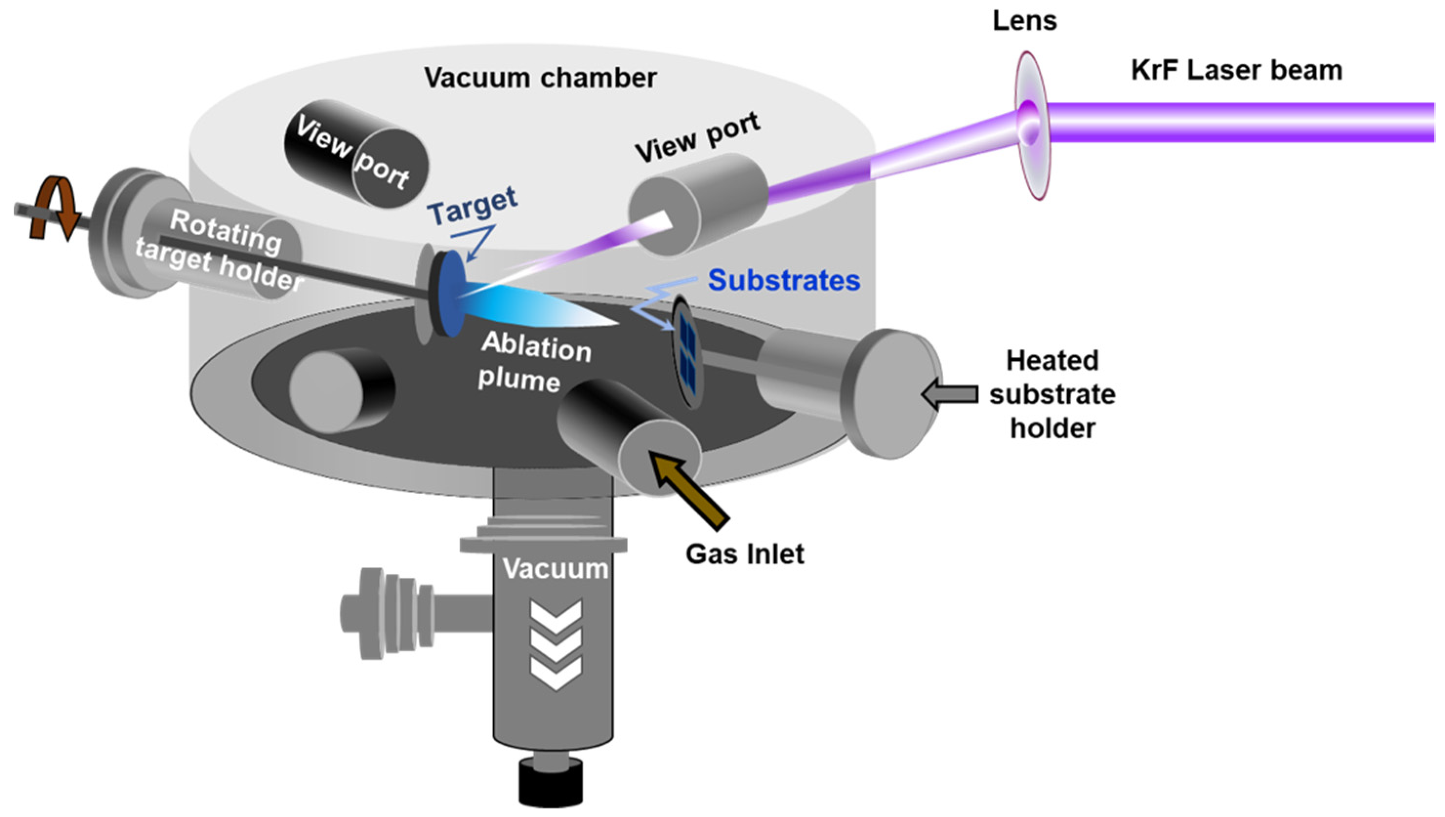
2.4. Pulsed Laser Deposition

Pulsed laser deposition (PLD) has emerged as one of the most promising physical vapor deposition (PVD) techniques for the deposition of MoS2 thin films. The PLD approach consists of shining a focused high-power laser beam onto the surface of a solid target to be ablated and deposited as a film on a substrate. PLD is a non-equilibrium process that leads to the absorption of very-short (15–20 ns) and highly-energetic laser pulses by the target and to the formation of a directive plasma plume. The laser-ablated species that form the plasma plume condense onto the substrate, leading to the growth of a thin film. The PLD is well known for its large process latitude, high-flexibility, and excellent process controllability. For instance, by controlling the number of laser ablation pulses and/or the background gas pressure, nanoparticles, and/or films with thicknesses varying from few nm to few microns can be synthesized. Figure 3 shows a schematic representation of a PLD system.
Among the advantages and the unique features of the PLD method, we can cite: (i) its ability to achieve a congruent transfer to the films when a multi-element target is used [91]; (ii) its highest instantaneous deposition rate along with the highly-energetic aspect of the ablated species (~10 times higher than in sputtering) enables the growth of metastable phases and/or crystalline phases even at room temperature; and (iii) its process latitude, which makes it easy to control almost independently each of the deposition parameters (laser intensity, number of laser ablation pulses, background gas pressure, and substrate temperature), and hence the properties of the deposited materials [92,93,94]. While the early studies on the PLD of MoS2 date back to the 1990s [95,96,97,98,99,100], it is only recently that important advancements have been made in PLD synthesis of 2D-MoS2 films onto various substrates opening thereby the way to their use for different optoelectronic applications. In 2014, PLD was successfully used to grow one to several layers of MoS2 onto different metal, semiconducting, and sapphire substrates [101,102]. Siegel et al. [103] were the first to report, in 2015, the growth of MoS2 films (from 1 to a few 10s of monolayers thick) on centimeter-sized areas. Other attempts were made to deposit ultrathin (≤3 nm) films of nearly-stoichiometric amorphous MoS2 onto irregular surfaces such as silicon and tungsten tips and to study their field electron emission (FEE) properties [95]. The authors stated that the addition of the MoS2 coating is beneficial to the FEE process since lower electric fields were required to extract an electron current density of 10 μA/cm2 (namely, 2.8 V/μm for MoS2-coated Si and ~5.5 V/μm for MoS2-coated W tips). More recently, PLD has been used to fabricate high-quality MoS2 films (monolayer to few layers) and integrated them into functional ultraviolet (UV) photodetectors [104]. The developed photodetectors were found to exhibit a very low dark current (~10 × 10−10 A), low operating voltage (2 V), and good response time (32 ms). Their performance surpassed that previously reported for 2D-MoS2 synthesized by other routes [105,106,107,108,109]. Indeed, under UV irradiation, their detectivity, photoresponse (Ion/Ioff ratio), and responsivity were found to be as high as 1.81 × 10¹⁴ Jones, 1.37 × 10⁵, and 3 × 10⁴ A/W, respectively. Table 5 summarizes most of the papers reported so far on the PLD of MoS2 films. More specifically, it compares the main PLD growth conditions of 2D-MoS2 films along with the obtained crystallographic phase and some of the reported optoelectronic properties.

2.5. Other Processing Routes

In addition to the main fabrication methods presented above, other PVD techniques have been used to deposit 2D-MoS2 films. Among these methods, magnetron sputtering has been used to deposit both MoS2 and WS2 films onto polydimethylsiloxane (PDMS) polymer substrates [37,127,128,129,130] with controllable defect densities. The PDMS substrate was chosen to fabricate flexible devices based on 2D-semiconducting materials. Interestingly, very smooth MoS2 surfaces, with a roughness of less than 2 nm, were achieved by casting the polymer on a polished silicon wafer. It has also been shown that it is possible to induce subsequent crystallization of MoS2 by exposing it to a pulsed 532 nm laser [127].
Finally, the use of any of the above-discussed techniques to fabricate 2D-MoS2 films is mostly dictated by the availability of the equipment, expertise, and requirements of targeted application. In a general context, the physical-chemical and optoelectronic properties of the final MoS2 films will be determined to select the appropriate synthesis route. Nevertheless, the level of complexity, throughput, and fabrication costs have to be considered to choose the appropriate synthesis technique particularly when a technology has to be adopted. Table 6 provides a general comparison of the preparation techniques of MoS2 described in this review by listing their main advantages and limitations.

3. Characterizations of MoS2 Thin Films

To assess the crystalline quality, microstructure, and optoelectronic properties of the synthesized 2D-MoS2, a variety of characterization techniques have been employed and reported in the literature. These include optical microscopy (OM), scanning electron microscopy (SEM), high-resolution transmission and Scanning transmission electron microscopy (HRTEM and HRSTEM), atomic force microscopy (AFM), energy-dispersive X-ray spectroscopy, X-ray photoelectron spectroscopy (XPS), Raman spectroscopy, and photoluminescence (PL). These methods are often used to investigate the overall 2D-MoS2 surface topography and to qualify the nature of the synthesized material and the shapes of its building blocks (i.e., triangle, nanosheets, and nanoplates) (Figure 4). The observations made by imaging methods are also essential to envision a possible growth mechanism of the micro/nanostructures with respect to the used processing parameters. For instance, Figure 4d shows a schematic representation of the nucleation process of some morphologies of 2D-MoS2.
Subsequently, HRTEM investigations could be carried out to precisely characterize the MoS2 crystalline structure and examine locally its lattice parameters and the presence of defects. In particular, the HRTEM image depicted in Figure 4e is of great importance, as it was recorded in cross-region containing the two possible crystal configurations of MoS2. As it can be seen in Figure 4e–g, the identified phase mixture of 1T@2H-MoS2 could coexist simultaneously in the same fabricated MoS2 thin film [131].
AFM and its variant methods constitute key characterization tools for the investigation of 2D crystals, mainly due to the atomically thin nature of this layered class of materials. Both vertical and lateral resolutions are fundamentally required to properly investigate the intrinsic properties of 2D materials. AFM is among the few techniques that allow the characterization of 2D-MoS2 in ambient and controlled environments at the nanometer scale. In addition to measuring the local thickness and surface topography, AFM-based electrical methods provide access to additional interesting properties such as the local variations in surface potential of 2D-MoS2. For instance, the Kelvin probe force microscopy (KPFM) method allows the characterization of the sample’s surface work function variations. The work function is an extreme surface property, which depends on the energy differences between the Fermi and vacuum levels at the surface. This renders the use of KPFM for the characterization of 2D-MoS2 fundamentally important to investigate band alignments in nanostructures and to study the dependencies of local electronic properties on the number of 2D-MoS2 layers. It also provides key insights into the environmental effects on the state of the sample surface both electronically and morphologically. The KPFM technique was used (Figure 5a) to determine the surface potential variations in mono- and multilayer MoS2, under different humidity conditions.
X-ray photoelectron spectroscopy (XPS) is another relevant surface characterization technique that is widely used to achieve the elemental surface composition of MoS2 films as well as their chemical bonding states. Figure 5b shows typical high-resolution XPS spectra of the Mo3d and S2p core levels. The Mo3d region exhibits two characteristic emission peaks at 232.5 (Mo 3d3/2) and 229.4 (Mo 3d5/2) eV. These binding energy values are consistent with electrons of Mo4++ corresponding to MoS2. Likewise, the S 2p3/2 and S 2p1/2 doublet appearing at binding energies of 162.3 and 163.5 eV is typical for S2- in MoS2 structure. Nan et al. [132] used XPS to show the PL enhancement of monolayer MoS2 through defect engineering and oxygen bonding. The chemical adsorption of oxygen created a heavy p-type doping and the conversion of the Trion into Excitons. Moreover, it caused the suppression of the non-radiative recombination of the excitons at the defect sites. Their results were verified by PL measurements at low temperature, as shown in Figure 5c,d.
Unlike bulk MoS2, the ultrathin 2D-MoS2 (i.e., one to few layers) exhibits a strong PL intensity which increases with reducing the number of layers [136], which has been attributed to quantum confinement effects [53,137]. The PL response can be tuned via several mechanisms including doping [134], plasmonic effect, and defects engineering [132]. For instance, Mouri et al. [134] studied the influence of the thickness on the PL response of MoS2 by using mono-, bi-, and trilayer MoS2 and the PL modulation using doping. They demonstrated that p-type doping with high electron affinity seems to enhance the PL intensity, while the n-type doping tends to reduce it, as illustrated in Figure 5c,d.
Moreover, Raman spectroscopy presents a very sensitive, fast, and non-destructive technique to access valuable information on the chemical structure, phase and polymorphs, crystallinity, and chemical bonding states of 2D-MoS2 materials. It allows the monitoring of the two characteristic peaks of MoS2, namely the in-plane and out-of-plane vibration modes E12g and A1g appearing for 514 nm excitation energy at the respective positions of 384.5 and 404.6 cm−1 for 2D-MoS2 monolayer [135] (Figure 5e). More interestingly, the difference between the peak positions of E12g, A1g (Δω) can be used as a robust and effective diagnostic to determine the number of MoS2 layers (up to four layers) or to simply estimate the MoS2 film thickness (Figure 5f). Usually, Δω is less than 20 cm−1 in the presence of a single layer of MoS2, but it increases with increasing MoS2 thickness to reach 25 cm−1 for the bulk MoS2 [135]. In fact, a thorough study on the dependence of the characteristic Raman peak positions, width, and intensity of MoS2 films on their thickness have been investigated [103,135,138]. Furthermore, H. Li et al. [138] reported that the frequency of the characteristic peaks is strongly dependent on the excitation energy due to the resonance effect. They showed a red shift of the E12g mode of about 2.2 cm−1 and blue shift of the A1g mode of about 4.1 cm−1. Thus, to effectively determine the exact MoS2 number of layers using Raman spectroscopy, one has to consider the excitation energy and the thickness limit at which the Raman vibrations frequency is reaching a plateau, indicating that it is less sensitive to MoS2 thickness variation above four layers.

4. Band Structures and Electronic Properties

We employed density functional theory (DFT) to determine the optoelectronic properties in particular the bandgap energy of both bulk and monolayer MoS2. Perdew–Burke–Ernzerhof (PBE) approach was applied to describe the electronic states of MoS2 using band structure and the density of states (DOS). DFT calculations were implemented in Quantum Espresso™ code [139,140]. The considered 2H-MoS2 has a hexagonal crystal form with the space group P63/mmc (No. 194). The equivalent positions for this structure employed in the calculations are Mo (1/3, 2/3, and 2/8) and S (1/3, 2/3, and 0.621). The valence electron configuration selected for Mo and S atoms are 4p5 5s1 and 3s2 3p4, respectively. The cutoff wave function and the cutoff charge densities are 70 and 700 Ryd, respectively [140]. The cell parameters and atomic positions were fully relaxed by the process of the total energy minimization. The values of the relaxed lattice constants for bulk MoS2 are a = 3.15 Å and c = 12.3 Å, respectively. The optimized structure was used to perform calculations for band structures and the total density of states for both MoS2 bulk and monolayer. For bulk MoS2 (top left panel of Figure 6a), 9 × 9 ×2 k-points were used to obtain the band structure along the path Γ-K-M-Γ in the Brillouin zone. For MoS2 monolayer (top right panel of Figure 6a), 9 × 9 × 1 k-points were used. A 15 Å vacuum along the z-axis above the monolayer was added to isolate the MoS2 and prevent any interaction between the adjacent layers [141]. The top view of the MoS2 monolayer is shown in the bottom panel of Figure 6a, where sulfur atoms are represented in yellow and molybdenum atoms are shown in purple.
To obtain the electronic properties, the MoS2 bulk was considered as a set of two hexagonal planes linked together by weak Van Der Waals bonds. The MoS2 monolayer was considered as a single hexagonal plane with covalent bonds between atoms S-Mo-S [142]. The left panel of Figure 6b shows the total DOS calculation results of the bulk MoS2 while the right panel of Figure 6b shows the calculation of its band structure. The energy range is between −8 and 4 eV versus the directions of the highest symmetries in the first Brillouin zone Γ, M, K, and Γ. As observed from the band structure calculations, the MoS2 bulk has an indirect bandgap of 0.9 eV. The minimum of the conduction band is located between K and G and the maximum of valence band at point G. This indirect bandgap obtained for the MoS2 bulk was attributed to the presence of interlayer interactions in the bulk structure [143]. In contrast, Figure 6c shows that the monolayer MoS2 has a direct bandgap of 1.89 eV at the K point. The DOS results are compatible with the results of the band structure. Similar conclusions have been stated in other investigations [141,142].

5. MoS2 Applications

Because of their attractive optoelectronic properties, possibly tunable by for example controlling the number of monolayers, MoS2 thin films were tested and validated for a variety of applications including electronics, photonics, solar energy, and energy storage. Here, we give a few examples of some specific successful and promising applications of MoS2 films for solar energy conversion [144,145], gas sensing [44,48,146,147], and plasmonics [148,149,150,151,152].

5.1. MoS2 for Solar Energy Harvesting

As demonstrated by DFT calculations, 2D-MoS2 exhibits interesting optoelectronic properties attributed to its direct bandgap ranging from 1.2 to 1.9 eV and an absorption coefficient greater than 105 cm−1 throughout the solar spectrum. These key properties are very promising for the use of MoS2 in photovoltaic (PV) applications. Indeed, it has been shown that, when a monolayer of n-type MoS2 is deposited onto a p-type silicon substrate, the resulting p-n junction based PV device is able to yield a power conversion efficiency (PCE) as high as 5.23%, as recorded elsewhere [153]. Such a PV performance is most likely a consequence of the excellent ability of MoS2 to efficiently separate the generated photo-charges at the n-MoS2/p-Si interface of the heterojunction.
To highlight the electrical performance of thin films MoS2-based solar cells in a homojunction form, we used the one-dimensional solar cell capacitance simulator SCAPS-1D™ software 3.3.08 interface [154], developed by M. Burgelman – Department of Electronics and Information Systems at the University of Ghent, Belgium [155,156], to calculate the different PV parameters, i.e., open circuit voltage VOC, short-circuit current density JSC, fill factor FF, and PCE (η). In this sense, a solar cell made of Ag/p-Si/MoS2/Al structure, as the one represented by a schematic in Figure 7, was implemented in the SCAPS-3308™ environment.
The simulations were made under AM1.5 illumination conditions at an operating temperature of 300 K. The physical parameters related to the electronic properties of the layers used in the simulation are shown in Table 7. For the considered junction, the thermal speed of the electrons and the holes were fixed at 107 cm/s, the type of defect is neutral, and the capture cross section is 10−14 cm2.
Beyond, the input parameters used in our SCAPS simulations, we provide hereinafter a survey of commonly used physical parameters of MoS2 reported in the literature to simulate the performance of MoS2 in PV applications. As can be seen in Table 8, several combinations are possible which may yield different results.
The outcome of our simulations shows that the p-Si/n-MoS2 structure in Figure 7 can yield a PCE value as high as 19.82% when considering 2D-MoS2 with the highest bandgap of 1.9 eV. Figure 8 shows the simulated J-V curve of the p-Si/n-MoS2 cell along with its associated PV parameters. The rather high Voc value of 0.64 V reflects the strong built-in electrical field at the interface between the n-MoS2 layer and p-Si substrate.
The high PCE obtained is comparable to the one obtained for well-proven solar cell materials. This is an outstanding yield for an only 0.33 nm thick material used in conjunction with p-Si in the solar cell set up as compared to 250 µm thickness used for conventional Si technology. Moreover, sulfur and molybdenum are abundant and cheaper raw materials as compared to the technologies achieving similar performances such as III-V materials.
Nevertheless, although the simulated PCE performance underlines the great potential of 2D-MoS2 films for PV devices, other challenging issues still need to be addressed or mitigated to develop such devices. For instance, the controlled deposition of MoS2 monolayer, the achievement of a reliable metal contact on MoS2 monolayer free of leakage current or a shortcut with the underlying Si substrate, and the scalability of 2D-MoS2 ultrathin films to the well-established large-size Si wafer technology are among the challenging issues to be addressed in future works.

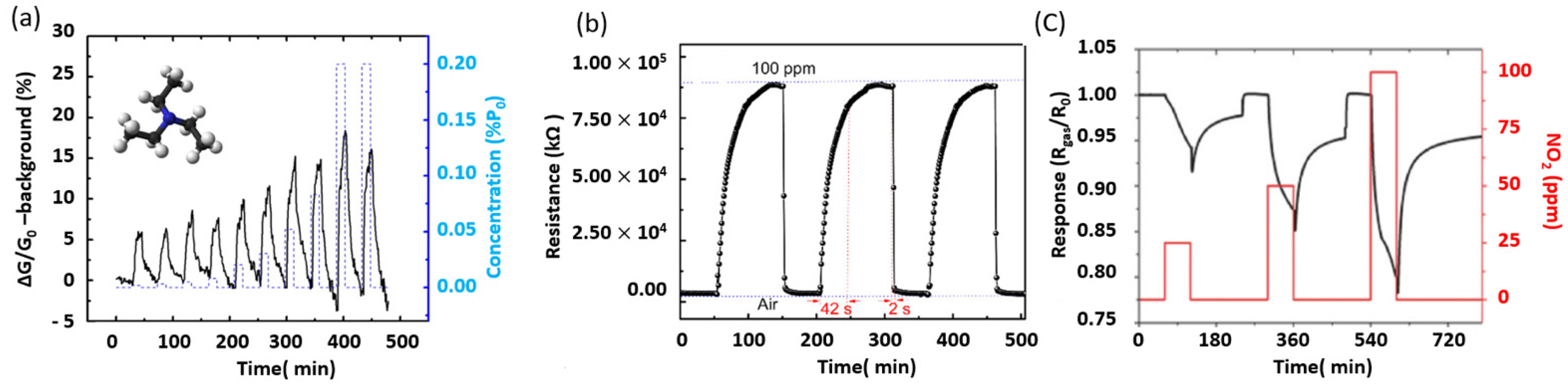
5.2. MoS2 for Gas Sensing Applications

MoS2 nanosheets (NS) have been reported to exhibit enhanced gas sensing performances for a variety of gases, including toxic and hazardous gases such as ammonia (NH3) and nitrogen dioxide (NO2) [43,48,146,165,166,167]. Thus, MoS2 NS act as a simple chemiresistor that changes its electrical resistance when in contact with reactive gases. The sensing response or sensitivity (S) towards a target gas, at a given operating temperature, is determined from the measured values of resistances of the MoS2-NS sensing element in the presence of atmospheric air resistance (Ra) and target gas (Rg). Usually, the target gas molecules adsorb onto the MoS2 NS exposed edges and changes its conductivity through the donor/acceptor exchanges process. The sensitivity (S) is defined as follows:
S = R a R g R g
To design an effective 2D-MoS2 gas sensor, care must be taken to the optimization of its operating temperature, response/recovery times, and selectivity. 2D-MoS2-based gas sensors were found to offer certain advantages, such as high-temperature stability, high resistance to a corrosive environment, and high sensitivity [26,146,165,166]. In addition, 2D-MoS2 thin film-based sensors were reported to detect NH3 triethylamine (TEA) molecules at the sub-ppm level, at an operating temperature as low as 30 °C [147].
MoS2 thin films obtained by mechanical exfoliation were used for highly sensitive field-effect transistor (FET) sensors [147]. By varying the number of MoS2 layers, the MoS2-based FET sensor exhibited high nitrogen monoxide (NO) sensitivity with a detection limit of 0.8 ppm. Moreover, DFT calculations indicated that NO and NO2 seemed to strongly bind to MoS2 nanosheets in contrast to other molecules such as carbon monoxide (CO), carbon dioxide (CO2), NH3, NO, NO2, and CH4. In addition, the exfoliated MoS2 monolayer showed high response to triethylamine (TEA) at concentrations ranging from 1 to 100 ppm at room temperature (Figure 9a). Due to the strong response and excellent signal-to-noise ratio, a detection limit of TEA as low as 10 ppb was achieved.
Furthermore, exfoliated few-layer MoS2 nanosheets deposited on a substrate with interdigitated electrodes demonstrated good NO2 detection performances at room temperature [168]. The reported device shows a quick and complete recovery time of 2 s at a rate greater than 97%. Similarly (Figure 9b), DFT calculations indicated that the fairly fast recovery of MoS2 arises from the weak van der Waals interactions between NO2 and the MoS2 surface.
It is worth mentioning that, regardless of their form or morphology, MoS2 thin films remain as robust gas sensors. Indeed, atomic layered MoS2 fabricated by CVD showed excellent sensitivity and high selectivity once exposed to NH3 and NO2 [169]. The resistance of the MoS2 films increases in the case of NO2 adsorption, while it decreases for the NH3 adsorption. The recovery rate of NO2 is higher at 100 °C than at room temperature, while the NH3 sensing signal is negligible at 100 °C. To further exploit the large affinity of NO2 with MoS2 thin films, MoS2 hexagonal-shaped nanoplates (HNPs), with exposed edges allowing significant charge transfer, were grown on the top 20 nm of carbon nanotubes (CNTs). This configuration is advantageous to increase both the surface area and the number of sites for gas adsorption. The hybridization of MoS2 by deposition on CNTs showed an enhanced room-temperature gas-sensing performance [42], attaining a detection limit of a few ppb of NO2 concentration.

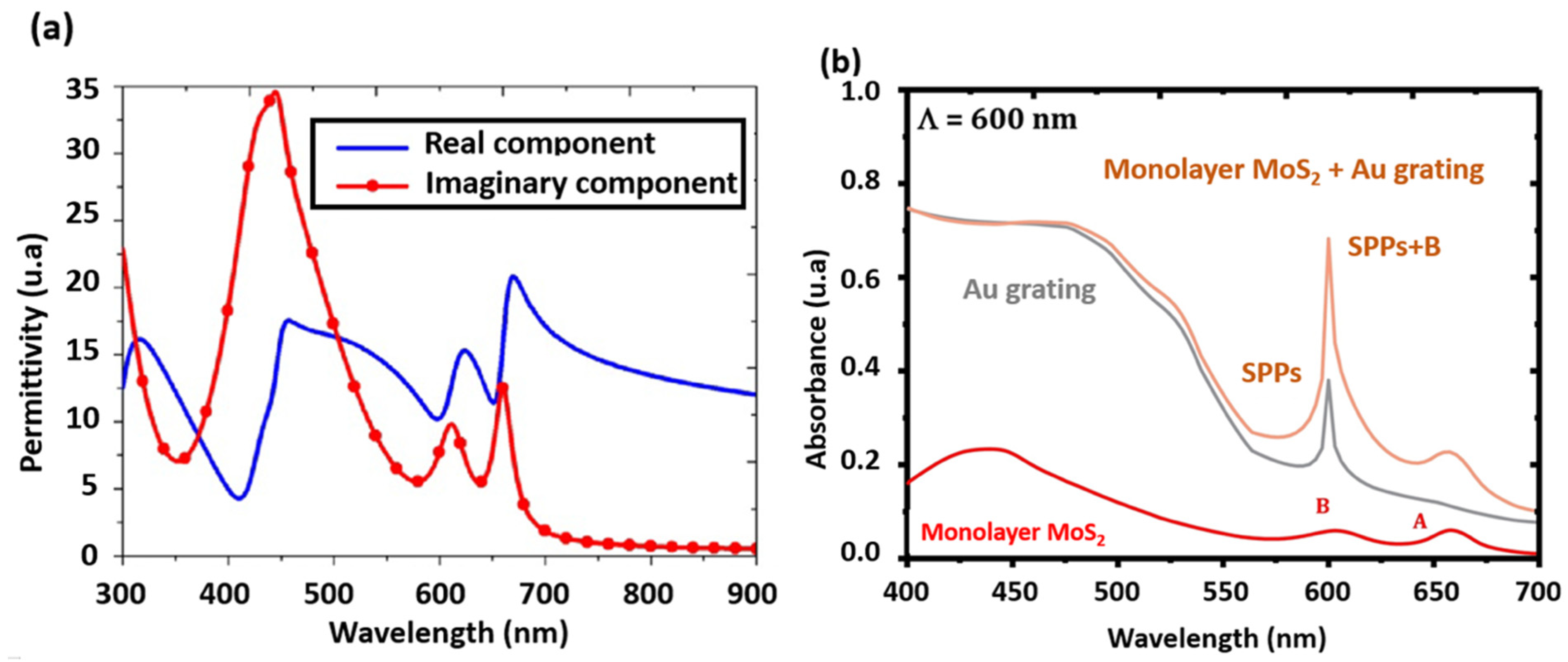
5.3. MoS2 for Plasmonic Applications

Because of their optical bandgap spread, MoS2 thin films offer interesting opportunities to be coupled with noble metal nanoparticles (NPs) in order to exacerbate the plasmonic properties. Indeed, the coupling effects between the excitons from MoS2 with the plasmons generated within the metal NPs open various prospects for tunable light emitters and absorbers over a wide spectrum. Various MoS2-related plasmonic structures have been developed for different optoelectronic applications, including photodetection [152], photoluminescence modulation [150], photocatalysis [170,171], and photovoltaics [172].
To better understand the origin of the enhancement in light emission/absorption properties of MoS2/metal-NPs hybrid structures, it is necessary to comprehend and estimate the variation of 2D-MoS2 complex permittivity. A mathematical approach based on hybrid Lorentz–Drude–Gaussian (HLDG) model was proposed by Mukherjee et al. [173] to describe the complex permittivity of MoS2 monolayer based on its absorption spectrum (Figure 10a).
The HLDG model can be presented as follows:
ε c = ε c L D + ε c G ,
where the superscripts LD and G correspond to Lorentz–Drude and Gaussian permittivity terms, respectively, as described elsewhere [173].
Chen et al. [176] used the HLDG model to design and simulate a perfect absorber based on the local surface plasmon resonance (LSPR) and the coupling properties between Ag patterns and a MoS2 monolayer. Their results show that MoS2 could increase the optical absorption dramatically. In another work, Jiang et al. [174] integrated the generalized interference theory in the HLDG model to investigate the optical properties of a broadband absorber utilizing a MoS2 monolayer. A more rigorous approach, consisting in the use of a coupled-wave analysis algorithm with the HLDG model, has been proposed to study the optical absorption of a composite photonic structure made of MoS2 Au grating [175]. The authors showed that the optical absorption of Au grating can be strongly modified by altering the number of MoS2 layers (Figure 10b), changing the layout of the MoS2 layer (e.g., to a MoS2 nanoribbon array), or inserting a hafnium dioxide spacer. Furthermore, they showed an enhancement of the localized electromagnetic field due to surface plasmon polaritons triggered by Au grating in the presence of few layers of MoS2. The observed enhancement of the MoS2 optical absorption was mainly attributed to the exciton transition. Additionally, the HLDG model was used by Xiaoyong et al. [149] to investigate the tunability of wave propagation in MoS2 supported hybrid surface plasmons waveguides based on dielectric fiber-gap metal substrate structures. By using the finite element method, these authors examined the influence of the structural parameters, the dielectric fiber shape and carrier concentration of the MoS2 layer on the hybrid modes. Their results allow identifying the tunable parameters of the hybrid modes of waveguide structures that could lead to the design of novel surface plasmon devices in the future.
On the other hand, the association of MoS2 with plasmonic NPs was also exploited by Yang et al. [151]. The authors reported on the fabrication of a hybrid nanostructure where a MoS2 monolayer is transferred onto the surface of 10-nm-wide Au nanogap arrays. Interestingly, by adjusting the length of the Au nanogaps, the authors achieved a photoluminescence enhancement as high as ~20 folds. In a more recent work, Mawlong et al. [150] also reported a much higher enhancement factor ~463 folds compared to pristine MoS2 monolayer at ambient of the PL intensity in the case of TiO2/Au/MoS2 ternary core–shell hetero-nanostructures. Such a strong PL enhancement was attributed to the heavy p-doping of the MoS2 lattice along with LSPR initiated exciton–plasmon coupling at the MoS2/Au interface [148]. These results suggest that the hybridization of MoS2 with appropriate metal nanostructures enhances the photoresponse. Indeed, Rahmati et al. [152] also reported an enhancement in the photocurrent generated by vertically aligned MoS2 nanosheets decorated with Au NPs.

6. Summary and Outlook

Based on the ever-increasing number of published works on 2D-TMDs materials, there is no doubt that MoS2 will continue to be one of the materials of the choice for the development of innovative and potentially scalable optoelectronic devices.
In term of fabrication, the CVD technique remains a comfortable and affordable route for continuous developments of a variety of shapes and morphologies of 2D-MoS2. By gaining more control of the deposition process itself, it is possible to further tune the optical and electrical properties of MoS2 nanostructures while increasing the size of the sample and the lateral uniformity. Of particular concern is the need to improve the reproducibility of defect-free structures. On the other hand, PLD appears as a highly promising alternative for the production of high-quality MoS2 thin films with a fairly high-level of homogeneity. It also allows tuning the MoS2 strain level during the elaboration, which may lead to exotic physical properties. PLD also offers an additional possibility to optimize, almost quasi-independently, different deposition parameters of MoS2 films, and hence tune at will their properties of interest. Finally, PLD also has the advantage of growing crystalline 2D-TMDS at room temperature, which opens the way to deposit MoS2 films onto flexible and thermo-sensitive substrates, thereby leading to a variety of new applications.
Regarding the applications, apart from those described in this review, 2D-MoS2 exhibits very appealing performances in infrared domains especially in combination with metamaterials such as passive radiative cooling. There are some emerging works [177,178,179,180] related to this aspect such as developing hybrid MoS2 thin films with new structures, including metamaterials, metasurfaces, photonic crystals, plasmonics, etc. Similarly, the development of 2D material-based antennas remains unsatisfactory as most of the known achievements on MoS2 in this domain are developed theoretically. Especially, the recent works [181] on terahertz (THz) plasmonics have shown the potential of MoS2 for their application in antenna research. Precisely, the use of MoS2 as a conductive medium in THz antenna appears as a potential direction of recent developments.

Author Contributions

Conceptualization, D.M., M.A.E.K., and M.J.; D.M. and A.K. contributed equally to this review; D.M. and G.D. synthesis and plasmonics; A.K and K.K. DFT calculations— SCAPS simulations and KPFM; M.E.M. PL and Raman spectroscopy; supervision, M.E.M., M.A.E.K., and M.J.; and writing—review and editing. All authors have read and agreed to the published version of the manuscript.

Funding

This research received no external funding.

Data Availability Statement

This review contains both data from literature and own authors’ work. The cited data can be consulted in the relevant cited article. The authors data: DFT calculations and SCAPS simulations are available upon request.

Acknowledgments

This work was done in the context of a scientific collaboration between INRS and UPJV. D.M. is grateful to both the Region HDF (France) and INRS (QC, Canada) for his PhD fellowship. The authors would like to acknowledge the financial support from the Natural Sciences and Engineering Research Council (NSERC) of Canada.

Conflicts of Interest

The authors declare no conflict of interest.

Abbreviations

1TTetragonal
2DTwo-dimension
2HHexagonal
3RRhombohedral
ΔωRaman shift between the peak positions of E12g and A1g
ALDAtomic layer deposition
A1gMoS2 out-of-plane Raman vibration mode
BLBuffer layer
CNTsCarbon nanotubes
CVDChemical vapor deposition
DFTDensity-functional theory
E12gMoS2 in-plane Raman vibration mode
ETLElectron transport layer
EQEExternal quantum efficiency
FEEField electron emission
FETField-effect transistor
GrGraphene
HITHeterojunction with intrinsic thin layer
HLDGHybrid Lorentz-Drude-Gaussian model
HNPsHexagonal-shaped nanoplates
HRTEMHigh-Resolution Transmission Electron Microscopy
J-Vcurrent density versus voltage
JscShort circuit current density
KPFMKelvin probe force microscopy
LSPRLocalized surface plasmon
NPsNanoparticles
NSsNanosheets
PCEPower conversion efficiency
PDMSPolydimethylsiloxane polymer
PLPhotoluminescence
PLDPulsed laser deposition
PPBParticles per billions
PPMParticles per millions
PSCsPerovskite solar cells
RaResistance of the sensing element in the presence of atmospheric air
RgResistance of the sensing element in the presence of the target gas
RHRelative humidity
SCsSolar cells
SEMScanning electron microscopy
SmaxThe maximum value of the sensing response
SPSurface potential
TCETransparent conducting electrode
TEMTransmission electron microscopy
TDThermal decomposition
TMDsTransition metal dichalcogenides
TRPLTime-resolved photoluminescence
TVDThermal vapor deposition
TVSThermal vapor sulfurization
UVUltraviolet
VocOpen circuit voltage
XPSX-ray photoelectron spectroscopy

References

  1. Mas-Ballesté, R.; Gómez-Navarro, C.; Gómez-Herrero, J.; Zamora, F. 2D materials: To graphene and beyond. Nanoscale 2011, 3, 20–30. [Google Scholar] [CrossRef] [PubMed]
  2. Allen, M.J.; Tung, V.C.; Kaner, R.B. Honeycomb carbon: A review of graphene. Chem. Rev. 2010, 110, 132–145. [Google Scholar] [CrossRef] [PubMed]
  3. Zhu, Y.; Murali, S.; Cai, W.; Li, X.; Suk, J.W.; Potts, J.R.; Ruoff, R.S. Graphene and graphene oxide: Synthesis, properties, and applications. Adv. Mater. 2010, 22, 3906–3924. [Google Scholar] [CrossRef] [PubMed]
  4. Mattevi, C.; Kim, H.; Chhowalla, M. A review of chemical vapour deposition of graphene on copper. J. Mater. Chem. 2011, 21, 3324–3334. [Google Scholar] [CrossRef]
  5. Deokar, G.; Avila, J.; Razado-Colambo, I.; Codron, J.L.; Boyaval, C.; Galopin, E.; Asensio, M.C.; Vignaud, D. Towards high quality CVD graphene growth and transfer. Carbon N. Y. 2015, 89, 82–92. [Google Scholar] [CrossRef]
  6. Deokar, G.; Casanova-Cháfer, J.; Rajput, N.S.; Aubry, C.; Llobet, E.; Jouiad, M.; Costa, P.M.F.J. Wafer-scale few-layer graphene growth on Cu/Ni films for gas sensing applications. Sens. Actuators B Chem. 2020, 305, 127458. [Google Scholar] [CrossRef]
  7. Minkin, A.S.; Lebedeva, I.V.; Popov, A.M.; Knizhnik, A.A. The Application of Empirical Potentials for Calculation of Elastic Properties of Graphene. Tech. Phys. Lett. 2019, 45, 111–114. [Google Scholar] [CrossRef]
  8. Gupta, A.; Sakthivel, T.; Seal, S. Recent development in 2D materials beyond graphene. Prog. Mater. Sci. 2015, 73, 44–126. [Google Scholar] [CrossRef]
  9. Castro Neto, A.H.; Guinea, F.; Peres, N.M.R.; Novoselov, K.S.; Geim, A.K. The electronic properties of graphene. Rev. Mod. Phys. 2009, 81, 109–162. [Google Scholar] [CrossRef] [Green Version]
  10. Neto Castro, A.H.; Novoselov, K. Two-dimensional crystals: Beyond graphene. Mater. Express 2011, 1, 10–17. [Google Scholar] [CrossRef]
  11. Tan, C.; Zhang, H. Two-dimensional transition metal dichalcogenide nanosheet-based composites. Chem. Soc. Rev. 2015, 44, 2713–2731. [Google Scholar] [CrossRef]
  12. Lu, Q.; Yu, Y.; Ma, Q.; Chen, B.; Zhang, H. 2D Transition-Metal-Dichalcogenide-Nanosheet-Based Composites for Photocatalytic and Electrocatalytic Hydrogen Evolution Reactions. Adv. Mater. 2016, 28, 1917–1933. [Google Scholar] [CrossRef] [PubMed]
  13. Ansari, L.; Monaghan, S.; McEvoy, N.; Coileáin, C.; Cullen, C.P.; Lin, J.; Siris, R.; Stimpel-Lindner, T.; Burke, K.F.; Mirabelli, G.; et al. Quantum confinement-induced semimetal-to-semiconductor evolution in large-area ultra-thin PtSe2 films grown at 400 °C. npj 2D Mater. Appl. 2019, 3, 1–8. [Google Scholar] [CrossRef] [Green Version]
  14. Stanford, M.G.; Rack, P.D.; Jariwala, D. Emerging nanofabrication and quantum confinement techniques for 2D materials beyond graphene. npj 2D Mater. Appl. 2018, 2, 1–15. [Google Scholar] [CrossRef] [Green Version]
  15. Butoi, C.I.; Langdon, B.T.; Kelley, D.F. Electron-Transfer Dynamics in DTDCI / MoS 2 and DTDCI / WS 2 Nanoclusters. J. Phys. Chem. B 1998, 102, 9635–9639. [Google Scholar] [CrossRef]
  16. Wu, X.L.; Fan, J.Y.; Qiu, T.; Yang, X.; Siu, G.G.; Chu, P.K. Experimental evidence for the quantum confinement effect in 3C-SiC nanocrystallites. Phys. Rev. Lett. 2005, 94, 1–4. [Google Scholar] [CrossRef] [PubMed] [Green Version]
  17. Gan, Z.X.; Liu, L.Z.; Wu, H.Y.; Hao, Y.L.; Shan, Y.; Wu, X.L.; Chu, P.K. Quantum confinement effects across two-dimensional planes in MoS2 quantum dots. Appl. Phys. Lett. 2015, 106, 233113. [Google Scholar] [CrossRef]
  18. Ellis, J.K.; Lucero, M.J.; Scuseria, G.E. The indirect to direct band gap transition in multilayered MoS 2 as predicted by screened hybrid density functional theory. Appl. Phys. Lett. 2011, 99, 261908. [Google Scholar] [CrossRef]
  19. Wang, S.W.; Medina, H.; Hong, K.B.; Wu, C.C.; Qu, Y.; Manikandan, A.; Su, T.Y.; Lee, P.T.; Huang, Z.Q.; Wang, Z.; et al. Thermally Strained Band Gap Engineering of Transition-Metal Dichalcogenide Bilayers with Enhanced Light-Matter Interaction toward Excellent Photodetectors. ACS Nano 2017, 11, 8768–8776. [Google Scholar] [CrossRef]
  20. Yu, Z.; Ong, Z.Y.; Li, S.; Xu, J.B.; Zhang, G.; Zhang, Y.W.; Shi, Y.; Wang, X. Analyzing the Carrier Mobility in Transition-Metal Dichalcogenide MoS2 Field-Effect Transistors. Adv. Funct. Mater. 2017, 27, 1604093. [Google Scholar] [CrossRef] [Green Version]
  21. Wang, S.; Zhao, W.; Giustiniano, F.; Eda, G. Effect of oxygen and ozone on p-type doping of ultra-thin WSe2 and MoSe2 field effect transistors. Phys. Chem. Chem. Phys. 2016, 18, 4304–4309. [Google Scholar] [CrossRef]
  22. Wang, X.; Wang, P.; Wang, J.; Hu, W.; Zhou, X.; Guo, N.; Huang, H.; Sun, S.; Shen, H.; Lin, T.; et al. Ultrasensitive and Broadband MoS2 Photodetector Driven by Ferroelectrics. Adv. Mater. 2015, 27, 6575–6581. [Google Scholar] [CrossRef] [Green Version]
  23. Yin, Z.; Zhang, X.; Cai, Y.; Chen, J.; Wong, J.I.; Tay, Y.Y.; Chai, J.; Wu, J.; Zeng, Z.; Zheng, B.; et al. Preparation of MoS2-MoO3 hybrid nanomaterials for light-emitting diodes. Angew. Chemie - Int. Ed. 2014, 53, 12560–12565. [Google Scholar]
  24. Liu, Z.; Liu, K.; Zhang, F.; Jain, S.M.; He, T.; Jiang, Y.; Liu, P.; Yang, J.; Liu, H.; Yuan, M. CH3NH3PbI3:MoS2 heterostructure for stable and efficient inverted perovskite solar cell. Sol. Energy 2020, 195, 436–445. [Google Scholar] [CrossRef]
  25. Wang, H.; Li, C.; Fang, P.; Zhang, Z.; Zhang, J.Z. Synthesis, properties, and optoelectronic applications of two-dimensional MoS2 and MoS2-based heterostructures. Chem. Soc. Rev. 2018, 47, 6101–6127. [Google Scholar] [CrossRef]
  26. Gupta, D.; Chauhan, V.; Kumar, R. A comprehensive review on synthesis and applications of molybdenum disulfide (MoS2) material: Past and recent developments. Inorg. Chem. Commun. 2020, 121, 108200. [Google Scholar] [CrossRef]
  27. Krishnan, U.; Kaur, M.; Singh, K.; Kumar, M.; Kumar, A. A synoptic review of MoS 2: Synthesis to applications. Superlattices Microstruct. 2019, 128, 274–297. [Google Scholar] [CrossRef]
  28. Nalwa, H.S. A review of molybdenum disulfide (MoS2) based photodetectors: From ultra-broadband, self-powered to flexible devices. RSC Adv. 2020, 10, 30529–30602. [Google Scholar] [CrossRef]
  29. Sun, J.; Li, X.; Guo, W.; Zhao, M.; Fan, X.; Dong, Y.; Xu, C.; Deng, J.; Fu, Y. Synthesis methods of two-dimensional MoS2: A brief review. Crystals 2017, 7, 198. [Google Scholar] [CrossRef]
  30. Kumar, R.; Sahoo, S.; Joanni, E.; Singh, R.K.; Yadav, R.M.; Verma, R.K.; Singh, D.P.; Tan, W.K.; Pérez del Pino, A.; Moshkalev, S.A.; et al. A review on synthesis of graphene, h-BN and MoS2 for energy storage applications: Recent progress and perspectives. Nano Res. 2019, 12, 2655–2694. [Google Scholar] [CrossRef]
  31. Xu, H.; Yi, J.; She, X.; Liu, Q.; Song, L.; Chen, S.; Yang, Y.; Song, Y.; Vajtai, R.; Lou, J.; et al. 2D heterostructure comprised of metallic 1T-MoS2/Monolayer O-g-C3N4 towards efficient photocatalytic hydrogen evolution. Appl. Catal. B Environ. 2018, 220, 379–385. [Google Scholar] [CrossRef]
  32. Backes, C.; Berner, N.C.; Chen, X.; Lafargue, P.; LaPlace, P.; Freeley, M.; Duesberg, G.S.; Coleman, J.N.; McDonald, A.R. Functionalization of liquid-exfoliated two-dimensional 2H-MoS2. Angew. Chemie - Int. Ed. 2015, 54, 2638–2642. [Google Scholar] [CrossRef] [PubMed]
  33. Tan, D.; Willatzen, M.; Wang, Z.L. Prediction of strong piezoelectricity in 3R-MoS2 multilayer structures. Nano Energy 2019, 56, 512–515. [Google Scholar] [CrossRef]
  34. Liu, K.K.; Zhang, W.; Lee, Y.H.; Lin, Y.C.; Chang, M.T.; Su, C.Y.; Chang, C.S.; Li, H.; Shi, Y.; Zhang, H.; et al. Growth of large-area and highly crystalline MoS 2 thin layers on insulating substrates. Nano Lett. 2012, 12, 1538–1544. [Google Scholar] [CrossRef] [Green Version]
  35. Yu, H.; Liao, M.; Zhao, W.; Liu, G.; Zhou, X.J.; Wei, Z.; Xu, X.; Liu, K.; Hu, Z.; Deng, K.; et al. Wafer-Scale Growth and Transfer of Highly-Oriented Monolayer MoS2 Continuous Films. ACS Nano 2017, 11, 12001–12007. [Google Scholar] [CrossRef] [PubMed]
  36. Yang, P.; Zhang, S.; Pan, S.; Tang, B.; Liang, Y.; Zhao, X.; Zhang, Z.; Shi, J.; Huan, Y.; Shi, Y.; et al. Epitaxial Growth of Centimeter-Scale Single-Crystal MoS2 Monolayer on Au(111). ACS Nano 2020, 14, 5036–5045. [Google Scholar] [CrossRef]
  37. Chen, X.P.; Xing, G.J.; Xu, L.F.; Lian, H.Q.; Wang, Y. Vertically aligned MoS2 films prepared by RF-magnetron sputtering method as electrocatalysts for hydrogen evolution reactions. Compos. Interfaces 2020, 1–10. [Google Scholar] [CrossRef]
  38. Hu, Z.; Wang, L.; Zhang, K.; Wang, J.; Cheng, F.; Tao, Z.; Chen, J. MoS2 Nanoflowers with Expanded Interlayers as High-Performance Anodes for Sodium-Ion Batteries. Angew. Chemie - Int. Ed. 2014, 53, 12794–12798. [Google Scholar] [CrossRef]
  39. Chen, J.; Kuriyama, N.; Yuan, H.; Takeshita, H.T.; Sakai, T. Electrochemical hydrogen storage in MoS2 nanotubes. J. Am. Chem. Soc. 2001, 123, 11813–11814. [Google Scholar] [CrossRef]
  40. Li, W.J.; Shi, E.W.; Ko, J.M.; Chen, Z.Z.; Ogino, H.; Fukuda, T. Hydrothermal synthesis of MoS2 nanowires. J. Cryst. Growth 2003, 250, 418–422. [Google Scholar] [CrossRef]
  41. Hwang, H.; Kim, H.; Cho, J. MoS2 nanoplates consisting of disordered graphene-like layers for high rate lithium battery anode materials. Nano Lett. 2011, 11, 4826–4830. [Google Scholar] [CrossRef]
  42. Deokar, G.; Vancsó, P.; Arenal, R.; Ravaux, F.; Casanova-Cháfer, J.; Llobet, E.; Makarova, A.; Vyalikh, D.; Struzzi, C.; Lambin, P.; et al. MoS2–Carbon Nanotube Hybrid Material Growth and Gas Sensing. Adv. Mater. Interfaces 2017, 4, 1–10. [Google Scholar] [CrossRef]
  43. Deokar, G.; Vignaud, D.; Arenal, R.; Louette, P.; Colomer, J. Synthesis and characterization of MoS2 nanosheets. Nanotechnology 2016, 27, 075604. [Google Scholar] [CrossRef]
  44. Deokar, G.; Rajput, N.S.; Vancsó, P.; Ravaux, F.; Jouiad, M.; Vignaud, D.; Cecchet, F.; Colomer, J.F. Large area growth of vertically aligned luminescent MoS2 nanosheets. Nanoscale 2017, 9, 277–287. [Google Scholar] [CrossRef]
  45. Gan, X.; Gao, Y.; Fai Mak, K.; Yao, X.; Shiue, R.J.; Van Der Zande, A.; Trusheim, M.E.; Hatami, F.; Heinz, T.F.; Hone, J.; et al. Controlling the spontaneous emission rate of monolayer MoS2 in a photonic crystal nanocavity. Appl. Phys. Lett. 2013, 103, 181119. [Google Scholar] [CrossRef] [PubMed] [Green Version]
  46. Eda, G.; Fujita, T.; Yamaguchi, H.; Voiry, D.; Chen, M.; Chhowalla, M. Coherent atomic and electronic heterostructures of single-layer MoS 2. ACS Nano 2012, 6, 7311–7317. [Google Scholar] [CrossRef] [PubMed]
  47. Wang, T.; Chen, S.; Pang, H.; Xue, H.; Yu, Y. MoS2-Based Nanocomposites for Electrochemical Energy Storage. Adv. Sci. 2017, 4, 1600289. [Google Scholar] [CrossRef] [PubMed]
  48. Shokri, A.; Salami, N. Gas sensor based on MoS2 monolayer. Sensors Actuators, B Chem. 2016, 236, 378–385. [Google Scholar] [CrossRef]
  49. Deokar, G.; Rajput, N.S.; Li, J.; Deepak, F.L.; Ou-Yang, W.; Reckinger, N.; Bittencourt, C.; Colomer, J.F.; Jouiad, M. Toward the use of CVD-grown MoS2 nanosheets as field-emission source. Beilstein J. Nanotechnol. 2018, 9, 1686–1694. [Google Scholar] [CrossRef] [Green Version]
  50. Ma, J.; Bai, H.; Zhao, W.; Yuan, Y.; Zhang, K. High efficiency graphene/MoS2/Si Schottky barrier solar cells using layer-controlled MoS2 films. Sol. Energy 2018, 160, 76–84. [Google Scholar] [CrossRef]
  51. Arulraj, A.; Ramesh, M.; Subramanian, B.; Senguttuvan, G. In-situ temperature and thickness control grown 2D-MoS2 via pulsed laser ablation for photovoltaic devices. Sol. Energy 2018, 174, 286–295. [Google Scholar] [CrossRef]
  52. Guo, F.; Li, M.; Ren, H.; Huang, X.; Hou, W.; Wang, C.; Shi, W.; Lu, C. Fabrication of p-n CuBi2O4/MoS2 heterojunction with nanosheets-on-microrods structure for enhanced photocatalytic activity towards tetracycline degradation. Appl. Surf. Sci. 2019, 491, 88–94. [Google Scholar] [CrossRef]
  53. Splendiani, A.; Sun, L.; Zhang, Y.; Li, T.; Kim, J.; Chim, C.Y.; Galli, G.; Wang, F. Emerging photoluminescence in monolayer MoS2. Nano Lett. 2010, 10, 1271–1275. [Google Scholar] [CrossRef] [PubMed]
  54. Eda, G.; Yamaguchi, H.; Voiry, D.; Fujita, T.; Chen, M.; Chhowalla, M. Photoluminescence from chemically exfoliated MoS 2. Nano Lett. 2011, 11, 5111–5116. [Google Scholar] [CrossRef] [PubMed]
  55. Rafiee, J.; Mi, X.; Gullapalli, H.; Thomas, A.V.; Yavari, F.; Shi, Y.; Ajayan, P.M.; Koratkar, N.A. Wetting transparency of graphene. Nat. Mater. 2012, 11, 217–222. [Google Scholar] [CrossRef]
  56. Kozbial, A.; Zhou, F.; Li, Z.; Liu, H.; Li, L. Are Graphitic Surfaces Hydrophobic? Acc. Chem. Res. 2016, 49, 2765–2773. [Google Scholar] [CrossRef]
  57. Marbou, K.; Ghaferi, A.A.; Jouiad, M. In-situ Characterization of Wettability Alteration in HOPG. SOP Trans. Nanotechnol 2015, 2374, 1–10. [Google Scholar]
  58. Huang, Y.; Pan, Y.H.; Yang, R.; Bao, L.H.; Meng, L.; Luo, H.L.; Cai, Y.Q.; Liu, G.D.; Zhao, W.J.; Zhou, Z.; et al. Universal mechanical exfoliation of large-area 2D crystals. Nat. Commun. 2020, 11, 1–9. [Google Scholar] [CrossRef]
  59. Magda, G.Z.; Petõ, J.; Dobrik, G.; Hwang, C.; Biró, L.P.; Tapasztó, L. Exfoliation of large-area transition metal chalcogenide single layers. Sci. Rep. 2015, 5, 3–7. [Google Scholar] [CrossRef] [Green Version]
  60. Kim, S.; Park, W.; Kim, D.; Kang, J.; Lee, J.; Jang, H.Y.; Song, S.H.; Cho, B.; Lee, D. Novel exfoliation of high-quality 2h-mos2 nanoflakes for solution-processed photodetector. Nanomaterials 2020, 10, 1045. [Google Scholar] [CrossRef]
  61. Pirzado, A.A.; Le Normand, F.; Romero, T.; Paszkiewicz, S.; Papaefthimiou, V.; Ihiawakrim, D.; Janowska, I. Few-layer graphene from mechanical exfoliation of graphite-based materials: Structure-dependent characteristics. ChemEngineering 2019, 3, 1–10. [Google Scholar] [CrossRef] [Green Version]
  62. Novoselov, K.S.; Jiang, D.; Schedin, F.; Booth, T.J.; Khotkevich, V.V.; Morozov, S.V.; Geim, A.K.; Benka, S.G. Two-dimensional atomic crystals. Phys. Today 2005, 58, 9. [Google Scholar] [CrossRef] [PubMed] [Green Version]
  63. Janica, I.; Iglesias, D.; Ippolito, S.; Ciesielski, A.; Samorì, P. Effect of temperature and exfoliation time on the properties of chemically exfoliated MoS2nanosheets. Chem. Commun. 2020, 56, 15573–15576. [Google Scholar] [CrossRef] [PubMed]
  64. Guan, Z.; Wang, C.; Li, W.; Luo, S.; Yao, Y.; Yu, S.; Sun, R.; Wong, C.P. A facile and clean process for exfoliating MoS2 nanosheets assisted by a surface active agent in aqueous solution. Nanotechnology 2018, 29, 425702. [Google Scholar] [CrossRef]
  65. Lin, H.; Wang, J.; Luo, Q.; Peng, H.; Luo, C.; Qi, R.; Huang, R.; Travas-Sejdic, J.; Duan, C.G. Rapid and highly efficient chemical exfoliation of layered MoS2and WS2. J. Alloys Compd. 2017, 699, 222–229. [Google Scholar] [CrossRef]
  66. Yang, Y.Q.; Tye, C.T.; Smith, K.J. Influence of MoS2 catalyst morphology on the hydrodeoxygenation of phenols. Catal. Commun. 2008, 9, 1364–1368. [Google Scholar] [CrossRef]
  67. Liu, H.F.; Wong, S.L.; Chi, D.Z. CVD Growth of MoS2-based Two-dimensional Materials. Chem. Vap. Depos. 2015, 21, 241–259. [Google Scholar] [CrossRef]
  68. Wang, Q.H.; Kalantar-Zadeh, K.; Kis, A.; Coleman, J.N.; Strano, M.S. Electronics and optoelectronics of two-dimensional transition metal dichalcogenides. Nat. Nanotechnol. 2012, 7, 699–712. [Google Scholar] [CrossRef]
  69. Zeng, T.; You, Y.; Wang, X.; Hu, T.; Tai, G. Chemical vapor deposition and device application of two-dimensional molybdenum disulfide-based atomic crystals. Prog. Chem. 2016, 28, 459–470. [Google Scholar]
  70. Balendhran, S.; Ou, J.Z.; Bhaskaran, M.; Sriram, S.; Ippolito, S.; Vasic, Z.; Kats, E.; Bhargava, S.; Zhuiykov, S.; Kalantar-Zadeh, K. Atomically thin layers of MoS 2via a two step thermal evaporation-exfoliation method. Nanoscale 2012, 4, 461–466. [Google Scholar] [CrossRef] [Green Version]
  71. Nam Trung, T.; Kamand, F.Z.; Al tahtamouni, T.M. Elucidating the mechanism for the chemical vapor deposition growth of vertical MoO2/MoS2 flakes toward photoelectrochemical applications. Appl. Surf. Sci. 2020, 505, 144551. [Google Scholar] [CrossRef]
  72. Ahn, C.; Lee, J.; Kim, H.U.; Bark, H.; Jeon, M.; Ryu, G.H.; Lee, Z.; Yeom, G.Y.; Kim, K.; Jung, J.; et al. Low-Temperature Synthesis of Large-Scale Molybdenum Disulfide Thin Films Directly on a Plastic Substrate Using Plasma-Enhanced Chemical Vapor Deposition. Adv. Mater. 2015, 27, 5223–5229. [Google Scholar] [CrossRef]
  73. Sojková, M.; Siffalovic, P.; Babchenko, O.; Vanko, G.; Dobročka, E.; Hagara, J.; Mrkyvkova, N.; Majková, E.; Ižák, T.; Kromka, A.; et al. Carbide-free one-zone sulfurization method grows thin MoS 2 layers on polycrystalline CVD diamond. Sci. Rep. 2019, 9, 2–12. [Google Scholar] [CrossRef] [Green Version]
  74. Withanage, S.S.; Kalita, H.; Chung, H.S.; Roy, T.; Jung, Y.; Khondaker, S.I. Uniform Vapor-Pressure-Based Chemical Vapor Deposition Growth of MoS2 Using MoO3 Thin Film as a Precursor for Coevaporation. ACS Omega 2018, 3, 18943–18949. [Google Scholar] [CrossRef] [PubMed] [Green Version]
  75. Wang, S.; Rong, Y.; Fan, Y.; Pacios, M.; Bhaskaran, H.; He, K.; Warner, J.H. Shape evolution of monolayer MoS2 crystals grown by chemical vapor deposition. Chem. Mater. 2014, 26, 6371–6379. [Google Scholar] [CrossRef]
  76. Jeon, J.; Jang, S.K.; Jeon, S.M.; Yoo, G.; Jang, Y.H.; Park, J.H.; Lee, S. Layer-controlled CVD growth of large-area two-dimensional MoS2 films. Nanoscale 2015, 7, 1688–1695. [Google Scholar] [CrossRef] [PubMed]
  77. Hyun, C.M.; Choi, J.H.; Lee, S.W.; Park, J.H.; Lee, K.T.; Ahn, J.H. Synthesis mechanism of MoS2 layered crystals by chemical vapor deposition using MoO3 and sulfur powders. J. Alloys Compd. 2018, 765, 380–384. [Google Scholar] [CrossRef]
  78. Lin, Z.; Zhao, Y.; Zhou, C.; Zhong, R.; Wang, X.; Tsang, Y.H.; Chai, Y. Controllable Growth of Large-Size Crystalline MoS2 and Resist-Free Transfer Assisted with a Cu Thin Film. Sci. Rep. 2015, 5, 1–10. [Google Scholar] [CrossRef] [PubMed] [Green Version]
  79. Rotunno, E.; Bosi, M.; Seravalli, L.; Salviati, G.; Fabbri, F. Influence of organic promoter gradient on the MoS2growth dynamics. Nanoscale Adv. 2020, 2, 2352–2362. [Google Scholar] [CrossRef] [Green Version]
  80. Le, D.; Rawal, T.B.; Rahman, T.S. Single-Layer MoS2 with Sulfur Vacancies: Structure and Catalytic Application. J. Phys. Chem. C 2014, 118, 5346–5351. [Google Scholar] [CrossRef]
  81. Jurca, T.; Moody, M.J.; Henning, A.; Emery, J.D.; Wang, B.; Tan, J.M.; Lohr, T.L.; Lauhon, L.J.; Marks, T.J. Low-Temperature Atomic Layer Deposition of MoS2 Films. Angew. Chemie - Int. Ed. 2017, 56, 4991–4995. [Google Scholar] [CrossRef]
  82. Tan, L.K.; Liu, B.; Teng, J.H.; Guo, S.; Low, H.Y.; Loh, K.P. Atomic layer deposition of a MoS2 film. Nanoscale 2014, 6, 10584–10588. [Google Scholar] [CrossRef] [PubMed]
  83. Mattinen, M.; Hatanpää, T.; Sarnet, T.; Mizohata, K.; Meinander, K.; King, P.J.; Khriachtchev, L.; Räisänen, J.; Ritala, M.; Leskelä, M. Atomic Layer Deposition of Crystalline MoS2 Thin Films: New Molybdenum Precursor for Low-Temperature Film Growth. Adv. Mater. Interfaces 2017, 4, 1700123. [Google Scholar] [CrossRef] [Green Version]
  84. Jin, Z.; Shin, S.; Kwon, D.H.; Han, S.J.; Min, Y.S. Novel chemical route for atomic layer deposition of MoS2 thin film on SiO2/Si substrate. Nanoscale 2014, 6, 14453–14458. [Google Scholar] [CrossRef]
  85. Browning, R.; Padigi, P.; Solanki, R.; Tweet, D.J.; Schuele, P.; Evans, D. Atomic layer deposition of MoS2 thin films. Mater. Res. Express 2015, 2, 12–17. [Google Scholar] [CrossRef]
  86. Liu, H.; Chen, L.; Zhu, H.; Sun, Q.Q.; Ding, S.J.; Zhou, P.; Zhang, D.W. Atomic layer deposited 2D MoS2 atomic crystals: From material to circuit. Nano Res. 2020, 13, 1644–1650. [Google Scholar] [CrossRef]
  87. Chen, C.; Raza, M.H.; Amsalem, P.; Schultz, T.; Koch, N.; Pinna, N. Morphology-Controlled MoS2 by Low-Temperature Atomic Layer Deposition. Nanoscale 2020, 12, 20404–20412. [Google Scholar]
  88. Yang, J.; Liu, L. Nanotribological properties of 2-D MoS2 on different substrates made by atomic layer deposition (ALD). Appl. Surf. Sci. 2020, 502, 144402. [Google Scholar] [CrossRef]
  89. Huang, Y.; Liu, L.; Sha, J.; Chen, Y. Size-dependent piezoelectricity of molybdenum disulfide (MoS2) films obtained by atomic layer deposition (ALD). Appl. Phys. Lett. 2017, 111, 063902. [Google Scholar] [CrossRef]
  90. Jang, Y.; Yeo, S.; Lee, H.B.R.; Kim, H.; Kim, S.H. Wafer-scale, conformal and direct growth of MoS 2 thin films by atomic layer deposition. Appl. Surf. Sci. 2016, 365, 160–165. [Google Scholar] [CrossRef]
  91. Pandiyan, R.; Oulad Elhmaidi, Z.; Sekkat, Z.; Abd-lefdil, M.; El Khakani, M.A. Reconstructing the energy band electronic structure of pulsed laser deposited CZTS thin films intended for solar cell absorber applications. Appl. Surf. Sci. 2017, 396, 1562–1570. [Google Scholar] [CrossRef]
  92. Brassard, D.; El Khakani, M.A. Pulsed-laser deposition of high- k titanium silicate thin films. J. Appl. Phys. 2005, 98, 054912. [Google Scholar] [CrossRef]
  93. Daghrir, R.; Drogui, P.; Dimboukou-Mpira, A.; El Khakani, M.A. Photoelectrocatalytic degradation of carbamazepine using Ti/TiO2 nanostructured electrodes deposited by means of a pulsed laser deposition process. Chemosphere 2013, 93, 2756–2766. [Google Scholar] [CrossRef]
  94. Ka, I.; Le Borgne, V.; Ma, D.; El Khakani, M.A. Pulsed laser ablation based direct synthesis of single-wall carbon nanotube/PbS quantum dot nanohybrids exhibiting strong, spectrally wide and fast photoresponse. Adv. Mater. 2012, 24, 6289–6294. [Google Scholar] [CrossRef]
  95. Late, D.J.; Shaikh, P.A.; Khare, R.; Kashid, R.V.; Chaudhary, M.; More, M.A.; Ogale, S.B. Pulsed laser-deposited MoS2 thin films on W and Si: Field emission and photoresponse studies. ACS Appl. Mater. Interfaces 2014, 6, 15881–15888. [Google Scholar] [CrossRef] [PubMed]
  96. Rai, R.H.; Pérez-Pacheco, A.; Quispe-Siccha, R.; Glavin, N.R.; Muratore, C. Pulsed laser annealing of amorphous two-dimensional transition metal dichalcogenides. J. Vac. Sci. Technol. A 2020, 38, 052201. [Google Scholar] [CrossRef]
  97. Wang, R.; Sun, P.; Wang, H.; Wang, X. Pulsed laser deposition of amorphous molybdenum disulfide films for efficient hydrogen evolution reaction. Electrochim. Acta 2017, 258, 876–882. [Google Scholar] [CrossRef]
  98. Loh, T.A.J.; Chua, D.H.C. Growth mechanism of pulsed laser fabricated few-layer MoS2 on metal substrates. ACS Appl. Mater. Interfaces 2014, 6, 15966–15971. [Google Scholar] [CrossRef] [PubMed]
  99. McDevitt, N.T.; Bultman, J.E.; Zabinski, J.S. Study of amorphous MoS2 films grown by pulsed laser deposition. Appl. Spectrosc. 1998, 52, 1160–1164. [Google Scholar] [CrossRef]
  100. Mosleh, M.; Laube, S.J.P.; Suh, N.P. Friction of undulated surfaces coated with mos2 by pulsed laser deposition. Tribol. Trans. 1999, 42, 495–502. [Google Scholar] [CrossRef]
  101. Serrao, C.R.; Diamond, A.M.; Hsu, S.L.; You, L.; Gadgil, S.; Clarkson, J.; Carraro, C.; Maboudian, R.; Hu, C.; Salahuddin, S. Highly crystalline MoS2 thin films grown by pulsed laser deposition. Appl. Phys. Lett. 2015, 106, 052101. [Google Scholar] [CrossRef]
  102. Barvat, A.; Prakash, N.; Singh, D.K.; Dogra, A.; Khanna, S.P.; Singh, S.; Pal, P. Mixed Phase Compositions of MoS2 Ultra Thin Film Grown by Pulsed Laser Deposition. Mater. Today Proc. 2018, 5, 2241–2245. [Google Scholar] [CrossRef]
  103. Siegel, G.; Venkata Subbaiah, Y.P.; Prestgard, M.C.; Tiwari, A. Growth of centimeter-scale atomically thin MoSfilms by pulsed laser deposition. APL Mater. 2015, 3, 056103. [Google Scholar] [CrossRef] [Green Version]
  104. Kumar, S.; Sharma, A.; Ho, Y.T.; Pandey, A.; Tomar, M.; Kapoor, A.K.; Chang, E.Y.; Gupta, V. High performance UV photodetector based on MoS2 layers grown by pulsed laser deposition technique. J. Alloys Compd. 2020, 835, 155222. [Google Scholar] [CrossRef]
  105. Lopez-Sanchez, O.; Lembke, D.; Kayci, M.; Radenovic, A.; Kis, A. Ultrasensitive photodetectors based on monolayer MoS 2. Nat. Nanotechnol. 2013, 8, 497–501. [Google Scholar] [CrossRef] [PubMed]
  106. Alkis, S.; Öztaş, T.; Aygün, L.E.; Bozkurt, F.; Okyay, A.K.; Ortaç, B. Thin film MoS_2 nanocrystal based ultraviolet photodetector. Opt. Express 2012, 20, 21815. [Google Scholar] [CrossRef] [PubMed] [Green Version]
  107. Huo, N.; Konstantatos, G. Ultrasensitive all-2D MoS2 phototransistors enabled by an out-of-plane MoS2 PN homojunction. Nat. Commun. 2017, 8, 1–6. [Google Scholar] [CrossRef]
  108. Tsai, D.S.; Liu, K.K.; Lien, D.H.; Tsai, M.L.; Kang, C.F.; Lin, C.A.; Li, L.J.; He, J.H. Few-layer MoS2 with high broadband photogain and fast optical switching for use in harsh environments. ACS Nano 2013, 7, 3905–3911. [Google Scholar] [CrossRef] [PubMed]
  109. Goel, N.; Kumar, R.; Roul, B.; Kumar, M.; Krupanidhi, S.B. Wafer-scale synthesis of a uniform film of few-layer MoS2 on GaN for 2D heterojunction ultraviolet photodetector. J. Phys. D. Appl. Phys. 2018, 51, 374003. [Google Scholar] [CrossRef]
  110. Donley, M.S.; Murray, P.T.; Barber, S.A.; Haas, T.W. Deposition and properties of MoS2 thin films grown by pulsed laser evaporation. Surf. Coatings Technol. 1988, 36, 329–340. [Google Scholar] [CrossRef]
  111. Walck, S.D.; Donley, M.S.; Zabinski, J.S.; Dyhouse, V.J. Characterization of Pulsed Laser Deposited PbO/MoS2 by Transmission Electron Microscopy. J. Mater. Res. 1994, 9, 236–245. [Google Scholar] [CrossRef]
  112. Barvat, A.; Prakash, N.; Satpati, B.; Singha, S.S.; Kumar, G.; Singh, D.K.; Dogra, A.; Khanna, S.P.; Singha, A.; Pal, P. Emerging photoluminescence from bilayer large-area 2D MoS2 films grown by pulsed laser deposition on different substrates. J. Appl. Phys. 2017, 122, 015304. [Google Scholar] [CrossRef]
  113. Wang, R.; Shao, Q.; Yuan, Q.; Sun, P.; Nie, R.; Wang, X. Direct growth of high-content 1T phase MoS2 film by pulsed laser deposition for hydrogen evolution reaction. Appl. Surf. Sci. 2020, 504, 144320. [Google Scholar] [CrossRef]
  114. Wang, S.; Yu, H.; Zhang, H.; Wang, A.; Zhao, M.; Chen, Y.; Mei, L.; Wang, J. Broadband few-layer MoS2 saturable absorbers. Adv. Mater. 2014, 26, 3538–3544. [Google Scholar] [CrossRef]
  115. Fominski, V.Y.; Markeev, A.M.; Nevolin, V.N.; Prokopenko, V.B.; Vrublevski, A.R. Pulsed laser deposition of MoSx films in a buffer gas atmosphere. Thin Solid Films 1994, 248, 240–246. [Google Scholar] [CrossRef]
  116. Jiao, L.; Jie, W.; Yang, Z.; Wang, Y.; Chen, Z.; Zhang, X.; Tang, W.; Wu, Z.; Hao, J. Layer-dependent photoresponse of 2D MoS 2 films prepared by pulsed laser deposition. J. Mater. Chem. C 2019, 7, 2522–2529. [Google Scholar] [CrossRef]
  117. Serna, M.I.; Yoo, S.H.; Moreno, S.; Xi, Y.; Oviedo, J.P.; Choi, H.; Alshareef, H.N.; Kim, M.J.; Minary-Jolandan, M.; Quevedo-Lopez, M.A. Large-Area Deposition of MoS2 by Pulsed Laser Deposition with in Situ Thickness Control. ACS Nano 2016, 10, 6054–6061. [Google Scholar] [CrossRef] [PubMed] [Green Version]
  118. Jiao, L.; Wang, Y.; Zhi, Y.; Cui, W.; Chen, Z.; Zhang, X.; Jie, W.; Wu, Z. Fabrication and Characterization of Two-Dimensional Layered MoS2 Thin Films by Pulsed Laser Deposition. Adv. Condens. Matter Phys. 2018, 2018, 23–28. [Google Scholar] [CrossRef] [Green Version]
  119. Pradhan, G.; Sharma, A.K. Anomalous Raman and photoluminescence blue shift in mono- and a few layered pulsed laser deposited MoS2 thin films. Mater. Res. Bull. 2018, 102, 406–411. [Google Scholar] [CrossRef]
  120. Walck, S.D.; Zabinski, J.S.; Donley, M.S.; Bultman, J.E. Evolution of surface topography in pulsed-laser-deposited thin films of MoS2. Surf. Coatings Technol. 1993, 62, 412–416. [Google Scholar] [CrossRef]
  121. Ho, Y.T.; Ma, C.H.; Luong, T.T.; Wei, L.L.; Yen, T.C.; Hsu, W.T.; Chang, W.H.; Chu, Y.C.; Tu, Y.Y.; Pande, K.P.; et al. Layered MoS2 grown on c -sapphire by pulsed laser deposition. Phys. Status Solidi - Rapid Res. Lett. 2015, 9, 187–191. [Google Scholar] [CrossRef]
  122. Zhang, Y.; Wang, S.; Yu, H.; Zhang, H.; Chen, Y.; Mei, L.; Di Lieto, A.; Tonelli, M.; Wang, J. Atomic-layer molybdenum sulfide optical modulator for visible coherent light. Sci. Rep. 2015, 5, 1–7. [Google Scholar] [CrossRef] [PubMed]
  123. Zhang, Y.; Wang, S.; Wang, D.; Yu, H.; Zhang, H.; Chen, Y.; Mei, L.; Di Lieto, A.; Tonelli, M.; Wang, J. Atomic-layer molybdenum sulfide passively modulated green laser pulses. IEEE Photonics Technol. Lett. 2016, 28, 197–200. [Google Scholar] [CrossRef]
  124. Miao, P.; Ma, Y.; Sun, M.; Li, J.; Xu, P. Tuning the SERS activity and plasmon-driven reduction of p-nitrothiophenol on a Ag@MoS2 film. Faraday Discuss. 2019, 214, 297–307. [Google Scholar] [CrossRef] [PubMed]
  125. Xie, M.Z.; Zhou, J.Y.; Ji, H.; Ye, Y.; Wang, X.; Jiang, K.; Shang, L.Y.; Hu, Z.G.; Chu, J.H. Annealing effects on sulfur vacancies and electronic transport of MoS2 films grown by pulsed-laser deposition. Appl. Phys. Lett. 2019, 115, 121901. [Google Scholar]
  126. Su, B.; He, H.; Ye, Z. Large-area ZnO/MoS2 heterostructure grown by pulsed laser deposition. Mater. Lett. 2019, 253, 187–190. [Google Scholar] [CrossRef]
  127. Pang, X.; Zhang, Q.; Shao, Y.; Liu, M.; Zhang, D.; Zhao, Y. A flexible pressure sensor based on magnetron sputtered mos2. Sensors (Switzerland) 2021, 21, 1130. [Google Scholar] [CrossRef]
  128. Tao, J.; Chai, J.; Lu, X.; Wong, L.M.; Wong, T.I.; Pan, J.; Xiong, Q.; Chi, D.; Wang, S. Growth of wafer-scale MoS2 monolayer by magnetron sputtering. Nanoscale 2015, 7, 2497–2503. [Google Scholar] [CrossRef]
  129. Kaindl, R.; Bayer, B.C.; Resel, R.; Müller, T.; Skakalova, V.; Habler, G.; Abart, R.; Cherevan, A.S.; Eder, D.; Blatter, M.; et al. Growth, structure and stability of sputter-deposited MoS2 thin films. Beilstein J. Nanotechnol. 2017, 8, 1115–1126. [Google Scholar] [CrossRef] [PubMed] [Green Version]
  130. Rowley-Neale, S.J.; Ratova, M.; Fugita, L.T.N.; Smith, G.C.; Gaffar, A.; Kulczyk-Malecka, J.; Kelly, P.J.; Banks, C.E. Magnetron Sputter-Coated Nanoparticle MoS2 Supported on Nanocarbon: A Highly Efficient Electrocatalyst toward the Hydrogen Evolution Reaction. ACS Omega 2018, 3, 7235–7242. [Google Scholar] [CrossRef]
  131. Tian, L.; Wu, R.; Liu, H.Y. Synthesis of Au-nanoparticle-loaded 1T@2H-MoS 2 nanosheets with high photocatalytic performance. J. Mater. Sci. 2019, 54, 9656–9665. [Google Scholar] [CrossRef]
  132. Nan, H.; Wang, Z.; Wang, W.; Liang, Z.; Lu, Y.; Chen, Q.; He, D.; Tan, P.; Miao, F.; Wang, X.; et al. Strong photoluminescence enhancement of MoS2 through defect engineering and oxygen bonding. ACS Nano 2014, 8, 5738–5745. [Google Scholar] [CrossRef] [Green Version]
  133. Feng, Y.; Zhang, K.; Li, H.; Wang, F.; Zhou, B.; Fang, M.; Wang, W.; Wei, J.; Wong, H.S.P. In situ visualization and detection of surface potential variation of mono and multilayer MoS2 under different humidities using Kelvin probe force microscopy. Nanotechnology 2017, 28, 295705. [Google Scholar] [CrossRef]
  134. Mouri, S.; Miyauchi, Y.; Matsuda, K. Tunable Photoluminescence of Monolayer MoS2 via Chemical Doping. Nano Lett. 2013, 13, 5944–5948. [Google Scholar] [CrossRef] [PubMed] [Green Version]
  135. Lee, C.; Yan, H.; Brus, L.E.; Heinz, T.F.; Hone, J.; Ryu, S. Anomalous lattice vibrations of single- and few-layer MoS2. ACS Nano 2010, 4, 2695–2700. [Google Scholar] [CrossRef] [Green Version]
  136. Mak, K.F.; Lee, C.; Hone, J.; Shan, J.; Heinz, T.F. Atomically thin MoS2: A new direct-gap semiconductor. Phys. Rev. Lett. 2010, 105, 2–5. [Google Scholar] [CrossRef] [PubMed] [Green Version]
  137. Cheiwchanchamnangij, T.; Lambrecht, W.R.L. Quasiparticle band structure calculation of monolayer, bilayer, and bulk MoS 2. Phys. Rev. B - Condens. Matter Mater. Phys. 2012, 85, 205302. [Google Scholar] [CrossRef] [Green Version]
  138. Li, H.; Zhang, Q.; Yap, C.C.R.; Tay, B.K.; Edwin, T.H.T.; Olivier, A.; Baillargeat, D. From bulk to monolayer MoS 2: Evolution of Raman scattering. Adv. Funct. Mater. 2012, 22, 1385–1390. [Google Scholar] [CrossRef]
  139. Ahmad, S.; Mukherjee, S. A Comparative Study of Electronic Properties of Bulk MoS2 and Its Monolayer Using DFT Technique: Application of Mechanical Strain on MoS2 Monolayer. Graphene 2014, 03, 52–59. [Google Scholar] [CrossRef] [Green Version]
  140. Erfanifam, S.; Jamilpanah, L.; Sangpour, P.; Haddadi, F.; Hamdi, M.; Erfanifam, M.; Chanda, G.; Herrmannsdörfer, T.; Sazgari, V.; Sadeghi, A.; et al. Electrical and optical properties of MoS2,MoOx=2,3(MoSO)/RGO heterostructure. arXiv 2018, 3, 1–6. [Google Scholar]
  141. Zhang, Z.; Qian, Q.; Li, B.; Chen, K.J. Interface Engineering of Monolayer MoS2/GaN Hybrid Heterostructure: Modified Band Alignment for Photocatalytic Water Splitting Application by Nitridation Treatment. ACS Appl. Mater. Interfaces 2018, 10, 17419–17426. [Google Scholar] [CrossRef]
  142. Dolui, K.; Rungger, I.; Das Pemmaraju, C.; Sanvito, S. Possible doping strategies for MoS2 monolayers: An ab initio study. Phys. Rev. B - Condens. Matter Mater. Phys. 2013, 88, 075420. [Google Scholar] [CrossRef] [Green Version]
  143. Zahid, F.; Liu, L.; Zhu, Y.; Wang, J.; Guo, H. A generic tight-binding model for monolayer, bilayer and bulk MoS 2. AIP Adv. 2013, 3, 052111. [Google Scholar] [CrossRef] [Green Version]
  144. Liang, M.; Ali, A.; Belaidi, A.; Hossain, M.I.; Ronan, O.; Downing, C.; Tabet, N.; Sanvito, S.; EI-Mellouhi, F.; Nicolosi, V. Improving stability of organometallic-halide perovskite solar cells using exfoliation two-dimensional molybdenum chalcogenides. npj 2D Mater. Appl. 2020, 4, 1–8. [Google Scholar] [CrossRef]
  145. Singh, E.; Kim, K.S.; Yeom, G.Y.; Nalwa, H.S. Atomically thin-layered molybdenum disulfide (MoS2) for bulk-heterojunction solar cells. ACS Appl. Mater. Interfaces 2017, 9, 3223–3245. [Google Scholar] [CrossRef]
  146. J rvinen, T.; Lorite, G.S.; Per ntie, J.; Toth, G.; Saarakkala, S.; Virtanen, V.K.; Kordas, K. WS2 and MoS2 thin film gas sensors with high response to NH3 in air at low temperature. Nanotechnology 2019, 30, 405501. [Google Scholar] [CrossRef] [Green Version]
  147. Perkins, F.K.; Friedman, A.L.; Cobas, E.; Campbell, P.M.; Jernigan, G.G.; Jonker, B.T. Chemical Vapor Sensing with Monolayer MoS2. Nano Lett. 2013, 13, 668–673. [Google Scholar] [CrossRef] [PubMed]
  148. Mukherjee, B.; Simsek, E. Utilization of monolayer MoS2 in Bragg stacks and metamaterial structures as broadband absorbers. Opt. Commun. 2016, 369, 89–93. [Google Scholar] [CrossRef]
  149. He, X.; Liu, F.; Lin, F.; Xiao, G.; Shi, W. Tunable MoS2 modified hybrid surface plasmon waveguides. Nanotechnology 2019, 30, 125201. [Google Scholar] [CrossRef] [PubMed]
  150. Mawlong, L.P.L.; Paul, K.K.; Giri, P.K. Exciton-plasmon coupling and giant photoluminescence enhancement in monolayer MoS2 through hierarchically designed TiO2/Au/MoS2 ternary core − Shell heterostructure. Nanotechnology 2021, 32, 215201. [Google Scholar] [CrossRef] [PubMed]
  151. Yang, Y.; Pan, R.; Tian, S.; Gu, C.; Li, J. Plasmonic hybrids of mos2 and 10-nm nanogap arrays for photoluminescence enhancement. Micromachines 2020, 11, 1109. [Google Scholar] [CrossRef]
  152. Rahmati, B.; Hajzadeh, I.; Taheri, M.; Karimzadeh, R.; Mohajerzadeh, S.; Mohseni, S.M. Plasmonic improvement photoresponse of vertical-MoS2 nanostructure photodetector by Au nanoparticles. Appl. Surf. Sci. 2019, 490, 165–171. [Google Scholar] [CrossRef]
  153. Tsai, M.L.; Su, S.H.; Chang, J.K.; Tsai, D.S.; Chen, C.H.; Wu, C.I.; Li, L.J.; Chen, L.J.; He, J.H. Monolayer MoS2 heterojunction solar cells. ACS Nano 2014, 8, 8317–8322. [Google Scholar] [CrossRef]
  154. Burgelman, M.; Verschraegen, J.; Minnaert, B.; Marlein, J. Numerical simulation of thin film solar cells: Practical exercises with SCAPS. Numos Work. 2007, 357–366. [Google Scholar]
  155. Burgelman, M.; Verschraegen, J.; Degrave, S.; Nollet, P. Modeling thin-film PV devices. Prog. Photovoltaics Res. Appl. 2004, 12, 143–153. [Google Scholar] [CrossRef]
  156. Verschraegen, J.; Burgelman, M. Numerical modeling of intra-band tunneling for heterojunction solar cells in scaps. Thin Solid Films 2007, 515, 6276–6279. [Google Scholar] [CrossRef]
  157. Chen, X.; Wu, Z.; Xu, S.; Wang, L.; Huang, R.; Han, Y.; Ye, W.; Xiong, W.; Han, T.; Long, G.; et al. Probing the electron states and metal-insulator transition mechanisms in molybdenum disulphide vertical heterostructures. Nat. Commun. 2015, 6, 1–8. [Google Scholar] [CrossRef] [Green Version]
  158. Rashid, H.; Rahman, K.S.; Hossain, M.I.; Tabet, N.; Alharbi, F.H.; Amin, N. Prospects of molybdenum disulfide (MoS2) as an alternative absorber layer material in thin film solar cells from numerical modeling. Chalcogenide Lett. 2014, 11, 397–403. [Google Scholar]
  159. Deng, Q.; Li, Y.; Shen, Y.; Chen, L.; Wang, G.; Wang, S. Numerical simulation on n-MoS2/p-Si heterojunction solar cells. Mod. Phys. Lett. B 2017, 31, 1750079. [Google Scholar] [CrossRef]
  160. Tousif, N.; Mohammad, S.; Ferdous, A.A.; Hoque, A. Investigation of Different Materials as Buffer Layer in CZTS Solar Cells Using SCAPS. J. Clean Energy Technol. 2018, 6, 293–296. [Google Scholar] [CrossRef] [Green Version]
  161. Heidariramsheh, M.; Haghighi, M.; Dabbagh, M.M.; Mahdavi, S.M. Pure sulfide Cu2ZnSnS4 layers through a one-step low-temperature PLD technique: Insight into simulation on modified back contact to overcome the barrier of MoS2. Mater. Sci. Eng. B Solid-State Mater. Adv. Technol. 2020, 262, 114701. [Google Scholar] [CrossRef]
  162. Bouarissa, A.; Gueddim, A.; Bouarissa, N.; Maghraoui-Meherezi, H. Modeling of ZnO/MoS2/CZTS photovoltaic solar cell through window, buffer and absorber layers optimization. Mater. Sci. Eng. B Solid-State Mater. Adv. Technol. 2021, 263, 114816. [Google Scholar] [CrossRef]
  163. Zaidi, B.; Ullah, M.S.; Hadjoudja, B.; Gagui, S.; Houaidji, N.; Chouial, B.; Shekhar, C. Role of TCO films in improving the efficiency of CdS/MoS 2 heterojunction solar cells. J. Nano- Electron. Phys. 2019, 11, 4–7. [Google Scholar] [CrossRef]
  164. Kohnehpoushi, S.; Nazari, P.; Nejand, B.A.; Eskandari, M. MoS2: A two-dimensional hole-transporting material for high-efficiency, low-cost perovskite solar cells. Nanotechnology 2018, 29, 205201. [Google Scholar] [CrossRef] [PubMed]
  165. Joshi, N.; Hayasaka, T.; Liu, Y.; Liu, H.; Oliveira, O.N.; Lin, L. A review on chemiresistive room temperature gas sensors based on metal oxide nanostructures, graphene and 2D transition metal dichalcogenides. Microchim. Acta 2018, 185, 1–16. [Google Scholar] [CrossRef] [PubMed]
  166. Donarelli, M.; Ottaviano, L. 2d materials for gas sensing applications: A review on graphene oxide, mos2, ws2 and phosphorene. Sensors (Switzerland) 2018, 18, 3638. [Google Scholar] [CrossRef] [PubMed] [Green Version]
  167. Ramanathan, A.A. Defect Functionalization of MoS2 nanostructures as toxic gas sensors: A review. IOP Conf. Ser. Mater. Sci. Eng. 2018, 305, 012001. [Google Scholar] [CrossRef] [Green Version]
  168. Li, W.; Zhang, Y.; Long, X.; Cao, J.; Xin, X.; Guan, X.; Peng, J.; Zheng, X. Gas Sensors Based on Mechanically Exfoliated MoS2 Nanosheets for Room-Temperature NO2 Detection. Sensors (Basel). 2019, 19, 2123. [Google Scholar] [CrossRef] [Green Version]
  169. Cho, B.; Hahm, M.G.; Choi, M.; Yoon, J.; Kim, A.R.; Lee, Y.J.; Park, S.G.; Kwon, J.D.; Kim, C.S.; Song, M.; et al. Charge-transfer-based gas sensing using atomic-layer MoS2. Sci. Rep. 2015, 5, 8052. [Google Scholar] [CrossRef]
  170. Zhang, Y.; Guo, S.; Xin, X.; Song, Y.; Yang, L.; Wang, B.; Tan, L.; Li, X. Plasmonic MoO2 as co-catalyst of MoS2 for enhanced photocatalytic hydrogen evolution. Appl. Surf. Sci. 2020, 504, 144291. [Google Scholar] [CrossRef]
  171. Li, Y.; Wang, H.; Xie, L.; Liang, Y.; Hong, G.; Dai, H. MoS2 Nanoparticles Grown on Graphene: An Advanced Catalyst for the Hydrogen Evolution Reaction. J. Am. Chem. Soc. 2011, 133, 7296–7299. [Google Scholar] [CrossRef] [Green Version]
  172. Chaojian, H.; Bo, L.; Qingwei, L.; Lijun, Y.; Yang, W.; Zhan, Y.; Lixin, D. Plasmon-Enhanced Photovoltaic Characteristics of Black Phosphorus-MoS 2 Heterojunction. IEEE Open J. Nanotechnol. 2021, 2, 41–51. [Google Scholar] [CrossRef]
  173. Mukherjee, B.; Tseng, F.; Gunlycke, D.; Amara, K.K.; Eda, G.; Simsek, E. Complex electrical permittivity of the monolayer molybdenum disulfide (MoS_2) in near UV and visible. Opt. Mater. Express 2015, 5, 447. [Google Scholar] [CrossRef] [Green Version]
  174. Jiang, Y.; Chen, W.; Wang, J. Broadband MoS 2 -based absorber investigated by a generalized interference theory. Opt. Express 2018, 26, 24403. [Google Scholar] [CrossRef] [PubMed]
  175. Song, J.; Lu, L.; Cheng, Q.; Luo, Z. Surface plasmon-enhanced optical absorption in monolayer MoS2 with one-dimensional Au grating. J. Quant. Spectrosc. Radiat. Transf. 2018, 211, 138–143. [Google Scholar] [CrossRef]
  176. Chen, W.; Wang, L.; Jiang, Y.; Wang, J. A Perfect Absorber Based on Monolayer MoS2 and Nano-Silver in the Visible Regime. 2018 Int. Conf. Microw. Millim. Wave Technol. (ICMMT). IEEE 2018, 1–3. [Google Scholar]
  177. Camellini, A.; Mazzanti, A.; Mennucci, C.; Martella, C.; Lamperti, A.; Molle, A.; Buatier de Mongeot, F.; Della Valle, G.; Zavelani-Rossi, M. Evidence of Plasmon Enhanced Charge Transfer in Large-Area Hybrid Au–MoS2 Metasurface. Adv. Opt. Mater. 2020, 8, 2000653. [Google Scholar] [CrossRef]
  178. Muhammad, N.; Chen, Y.; Qiu, C.W.; Wang, G.P. Optical Bound States in Continuum in MoS2-Based Metasurface for Directional Light Emission. Nano Lett. 2021, 21, 967–972. [Google Scholar] [CrossRef]
  179. Deng, M.; Li, Z.; Rong, X.; Luo, Y.; Li, B.; Zheng, L.; Wang, X.; Lin, F.; Meixner, A.J.; Braun, K.; et al. Light-Controlled Near-Field Energy Transfer in Plasmonic Metasurface Coupled MoS2 Monolayer. Small 2020, 16, 2003539. [Google Scholar] [CrossRef]
  180. Liu, J.T.; Tong, H.; Wu, Z.H.; Huang, J.B.; Zhou, Y.S. Greatly enhanced light emission of MoS2 using photonic crystal heterojunction. Sci. Rep. 2017, 7, 1–8. [Google Scholar] [CrossRef] [Green Version]
  181. Xie, Y.; Liang, F.; Chi, S.; Wang, D.; Zhong, K.; Yu, H.; Zhang, H.; Chen, Y.; Wang, J. Defect Engineering of MoS2 for Room-Temperature Terahertz Photodetection. ACS Appl. Mater. Interfaces 2020, 12, 7351–7357. [Google Scholar] [CrossRef] [PubMed]
Figure 1. (a) Top view of 2H/1T MoS2 monolayer. (b) Polymorphic structures of MoS2 (2H is the hexagonal crystal form, 1T is the tetragonal crystal form, and 3R is the rhombohedral crystal form).
Materials 14 03283 g001
Figure 2. Schematic of the chemical vapor deposition techniques: (a) thermal vapor sulfurization process using a quartz tube; (b) thermal vapor deposition process using a quartz tube; and (c) thermal decomposition of (NH4)2MoS4 (reproduced and adapted from Ref. [34]).
Materials 14 03283 g002
Figure 3. Schematic of the pulsed laser deposition chamber.
Materials 14 03283 g003
Figure 4. Examples of MoS2 microstructures: (a) planar triangle flakes scale = 40 µm; (b) vertical nanosheets scale = 100 um; (c) vertical nanoplates scale = 100 µm; (d) schematic of the nucleation process of MoS2; (e) HRTEM image of mixed 1T-MoS2 and 2H-MoS2; (f) zoom in of blue circled region of the 1T-MoS2 structure, with the unit cell of the 1T phase; and (g) zoom in of red circled region of the 2H-MoS2 structure, with the unit cell of the 2H phase. (Figure 4e–g adapted from Ref. [131] Copyright 2019, Springer Nature.)
Materials 14 03283 g004
Figure 5. (a) Surface potential captured by KPFM vs. relative humidity RHs with respect of the number of MoS2 layers (reproduced and adapted from Ref. [133], Copyright 2017, IOP Publishing); (b) XPS spectra of Mo 3d and S 2s core levels for different treatment conditions (adapted from Ref. [132] Copyright 2014, American Chemical Society); (c,d) PL spectra of monolayer MoS2 before and after being doped (reproduced from Ref. [134] Copyright 2013, American Chemical Society); and (e,f) Raman spectra for various MoS2 films with respect to the number of MoS2 layers (reproduced from Ref. [135] Copyright 2010, American Chemical Society).
Materials 14 03283 g005
Figure 6. (a) Bulk MoS2 (top-left), monolayer MoS2 (top-right), and top view of MoS2 monolayer (bottom). Total density of states (left) and band structure (right) of the (b) bulk and (c) monolayer.
Materials 14 03283 g006
Figure 7. Simulated solar cell structure of solar cell.
Materials 14 03283 g007
Figure 8. Simulated J-V characteristic of p-Si/n-MoS2 solar cell, as calculated by SCAPS-1D™ software.
Materials 14 03283 g008
Figure 9. (a) MoS2 sensor response exposed to TEA (adapted from Ref. [147] Copyright 2013, American Chemical Society); (b) repeatability and reversibility of the FLMN gas sensor at 100 ppm NO2 concentration (reproduced and adapted from Ref. [168], Copyright 2019, MDPI); and (c) the MoS2/CNT sensor response as a function of three NO2 concentrations (25, 50, and 100 ppm) (reproduced and adapted from Ref. [42], Copyright 2017, Wiley-VCH).
Materials 14 03283 g009
Figure 10. (a) Complex permittivity vs. wavelength of monolayer MoS2 (reproduced and adapted from [174], Copyright 2018, The Optical Society, OSA); and (b) spectral absorptances of an opaque Au plate, a simple 1D Au grating, a suspended monolayer MoS2, and monolayer MoS2-covered Au grating for TM waves with normal incidence from 400–700 nm (reproduced from Ref. [175] Copyright 2018, Elsevier).
Materials 14 03283 g010
Table 1. Crystal parameters and the nature of polymorphic structures of 2D-MoS2.
Polymorphic StructureLattice ParameterPoint GroupElectronic BehaviorRef
1Ta = 5.60 Å, c = 5.99 ÅD6dMetal[31]
2Ha = 3.15 Å, c = 12.30 ÅD6hSemiconductor[32]
3Ra = 3.17 Å, c = 18.38 Å.C3vSemiconductor[33]
Table 2. Examples of CVD-TVS grown MoS2 nanostructures.
SubstratePrecursorsGrowth ConditionsMorphologyRef
SiMoO3 and S powders dispersed on substrateMoO3 and S powders dispersed on substrate at 850 °C; S powder at 400 °C; Ar-0.725 L/min; time reaction = 30 minMoS2 nanosheets[43]
Si [001]S powder and Mo film deposited on substrateMo deposited on Silicon at 850 °C, S at 400 °C; Ar-0.725 L/min; time reaction = 30 minMoS2 nanosheets[44]
Si/SiO2S powder and Mo film deposited on substrateMo deposited on Silicon at 850 °C, S at 400 °C; Ar-0.725 L/min; time reaction = 30 minMoS2 nanosheets[49]
Diamond substrateS powder and Mo deposited on substrateMo deposited on Silicon with S powder at 800 °C; N2; ambient pressure; time reaction = 30 minHorizontally and vertically MoS2[73]
Si/SiO2S powder and MoO3 deposited on substrateMoO3 film deposited on Silicon at 750–850 °C, 600 mg of S powder at 100 °C; Ar-0.01 L/min; time reaction = 10 minMono-to few-layers of MoS2[74]
Table 3. Examples of TVD grown MoS2 along with their relevant processing conditions (* D is the distance between the MoO3 and S powders inside the tubular furnace).
Substrate/SetupMoO3 (mg)S (mg)D * (cm)Gas, Flow (sccm)T (°C), Time (min)MorphologyRef
Si face-down158018Ar
10 to 500
700, 30Flake size between 5.1–47.9 µm[75]
SiO2/Si
face-up
1020030Ar, 100850, 20Monolayer, bilayer and trilayer MoS2[76]
SiO2/Si
face-down
10100N2, 20650, 20MoS2 monolayer[77]
SiO2/Si
face-down
10-3025Ar, 150800, 10MoS2 triangular flakes[78]
SiO2/Si
face-up
50175N2, 300750, 15MoS2 monolayer with lateral size of 50 µm[79]
Table 4. Summary of the ALD deposition conditions and achieved MoS2 film thicknesses.
SubstratePrecursorsP (Torr)T (°C)CyclesThicknessRef
SiO2/SiMo hexacarbonyl and dimethyldisulfide1.4–3.3100100≈11 nm[84]
SiO2/n-SiMoCl5 and H2S0.75350–450100≈9 nm[85]
Al2O3Mo(NMe2)4 and H2S60100≈12 nm[81]
Al2O3 2-inch waferMoCl5 and H2S0.00130050≈9 nm[82]
SiO2/SiMo(thd)3 (thd = 2,2,6,6 tetramethylheptane 3,5-dionato) and H2S3.75300100≈25 nm[83]
Al2O3
c-plane
MoCl5 and hexamethyldisilathiane3.75350250≈22 nm[86]
Carbon nanotubes, Si-wafers and glassbis(tbutylimino)bis(dimethylamino) Mo (VI) and H2S300100–250100≈11 nm[87]
Si, SiO2, Al2O3MoCl5 and H2S3.75430–48011 layer[88]
SiMoCl5 and H2S390–480100≈21.5 nm[89]
SiO2Mo hexacarbonyl and H2S175100≈5 nm[90]
Table 5. Summary of the PLD conditions of MoS2 films along with their thickness and some of their properties.
SubstrateTargetP(Pa)T(°C)Laser EnergyThicknessPropertiesRef
Stainless steelMoS22.66 × 10−6RT/200/300/4505 mJ≈400 nmGranular structure stoichiometric, crystalline MoS2[110]
Stainless steelMoS210−6RT/300100 mJ≈70 nmStoichiometric single crystal MoS2 [111]
c-Al2O3 (0001) and Si/SiO22H-MoS29.33 × 10−4600500 mJ/cm2≈1.4 nmStoichiometric 2H phase
Flake size ≈ 10 µm
[112]
GaN/c-Al2O3 (0001)2H-MoS28 × 10−470050 mJFew layersMixed phase
Roughness ≈0.11 nm
[102]
Titanium foilp-MoS21.33 × 10−2RT0.65 nm1T phase MoS2[113]
SiO2 on Si [100]MoS21.33 × 10−2800200 mJ/cm2≈20–60 nm2H phase MoS2[104]
Gold-coated carbon clothAmorphous MoS21.33 × 10−2RT220 mJ/cm2≈200 nm2H phase MoS2[97]
QuartzMoS29 × 10−53008500 mJ/cm230 layersMixed phase[114]
Al2O3 (0001)MoS2+S
Powder
1.33 × 10−270050 mJ1–15 Layers of MoS2p-MoS2
2H phase MoS2
Roughness of 0.27 nm
[101]
SiMoS24 × 10−4RT5/10/100/400 mJ/cm2≈100–200 nmVarious compositions of MoSx (x ≤ 2.2)[115]
SiO2MoS23 × 10−5700200 mJ1–5 layers2H phase MoS2[116]
W (100)-tipMoS2+poly(vinl)5 × 10 3 7002000 mJ/cm2≈20–60 nmnearly stoichiometric 2H phase MoS2[95]
n-Si and p-SiMoS2+poly(vinl)5 × 10 3 700500 mJ/cm2≈20–60 nmnearly stoichiometric 2H phase MoS2[95]
Al, Ag, Ni, CuMoS22.6 × 10−550050 mJ≈5 nmEpitaxial growth of 2H phase MoS2[98]
Sapphire
Quartz
SiO2
HfO2
MoS2 +S powder1.33 × 10−270030 mJ1 monolayer—2.8 nmlarge-area growth of stoichiometric layered 2H phase MoS2[117]
SiO2/SiMoS210−5700200 mJfew-layer2H phase MoS2[118]
SiO2/SiMoS2 powder5 × 10−46002200 mJ/cm213 nmEpitaxial growth of 2H phase MoS2[119]
SiMoS210−4RT100 mJ129–1900 nmStoichiometric films[120]
c-plane sapphireMoS210−38002000–3000 mJ/cm21–5 layersEpitaxial growth of 2H phase MoS2[121]
Quartz glassPolycrystalline MoS2 powder5 × 10−43008500 mJ/cm29–10 monolayersnearly stoichiometric 2H phase MoS2[122]
QuartzMoS28.9 × 10−5 600 mJ≈5.8 nm2H phase MoS2[123]
SiO2/SiMoS2@Ag1.33 × 10−75001000–2000 mJ/cm2≈1.3–12.8 nm2H phase MoS2[124]
fluorophlogopite micaMoS210−57004000 mJ/cm2≈3.3 nm2H phase MoS2[125]
Al2O3 (0001)MoS210−3650100 mJ≈400 nm2H phase MoS2[126]
Table 6. Comparison of the advantages and limitations of different preparation techniques of MoS2.
TechniquesAdvantagesLimitations
Mechanical exfoliation
-
High-quality and good crystallinity.
-
Mono- to few-layer MoS2
-
Simple process
-
Long processing time (8–84 h)
-
Tedious and no controllability
-
Difficult integration with micro/optoelectronic processing
Chemical exfoliation
-
Large-scale growth
-
Synthesis of MoS2 monolayer
-
Loss of semiconducting properties of MoS2 during Li intercalation.
Chemical vapor deposition
-
High-quality and crystallinity
-
Centimeter-scale area growth
-
Good control of morphologies
-
Caution due to the use of toxic precursors
-
High synthesis temperatures requirement
-
No lateral uniformity
-
Mixed phases of 1T, 2H, etc.
Atomic layer deposition
-
Low-temperature deposition
-
Uniformity of MoS2 films
-
High quality of uniformity
-
Excellent step coverage
-
Very low throughput
-
Long processing time
-
High cost
Pulsed laser deposition
-
High-quality and faithful transfer of film stoichiometry
-
Nanometer-level control of the film thickness
-
Uniformity onto a large surface (up to 3” or 4” diameter wafers)
-
Quasi-independent control of the growth parameters.
-
Room-temperature deposition of crystallized MoS2
-
Compatibility with electronic and optoelectronic device processing
-
Relatively costly
-
Presence of ablated particulates on the surface
Sputtering
-
High quality and uniformity onto large surface
-
Compatibility with electronic and optoelectronic device processing.
-
Fair thickness control
-
Relatively costly
-
Preferential sputtering
-
Less control on the stoichiometry
Table 7. Physical parameters of n-MoS2 monolayer and p-Si substrate used in the SCAPS-1D™ simulations.
Parametersp-Si [SCAPS]n-MoS2
Thickness (nm)2000.32
Bandgap (eV)1.121.9 [153]
Electron affinity (eV)4.54.2 [153]
Dielectric permittivity (relative)11.910.5 [157]
CB effective density of states (1/cm3)2.8 × 10192.2 × 1018 [158]
VB effective density of states (1/cm3)1.04 × 10191.8 × 1019 [158]
Electron thermal velocity (cm/s)1 × 1071 × 107 [159]
Hole thermal velocity (cm/s)1 × 1071 × 107 [159]
Electron mobility (cm2/Vs)1500150 [20]
Hole mobility (cm2/Vs)450086 [159]
Shallow uniform donor density (1/cm3)01 × 1017 [159]
Shallow uniform acceptor density NA (1/cm3)1 × 10160
Table 8. A survey of the physical parameters of MoS2 used for the simulation of photovoltaic applications.
PV ParametersReported Values and References
Bandgap1.29 eV [158,160,161] 1.2–1.8 eV [159]1.23 eV [162]1.8 eV [163]
Electron affinity4.2 eV [158,160,161,162,163]4–4.7 eV [159]4.22 eV [163]
Relative dielectric permittivity3 [164]4 [160,161,162]7 [159]13.6 [158]
Effective density of states in conduction band1016 cm−3 [163] 7.5 × 1017 cm−3 [160,162]2.2 × 1018 cm−3 [158,161]1019, 2.5 × 1020 cm−3 [159,164]
Effective density of states in valance band1017 cm−3 [163]1.8 × 1018 cm [160,162]~1019 cm−3 [158,161,164]2.5 × 1020 cm−3 [159]
Electron thermal velocity105 cm/s [162]2.12 × 107 cm/s
Hole thermal velocity107 cm/s [162]1.18 × 107 cm/s [161]
Electron mobility44 cm2/Vs [159]50 cm2/Vs [161]100 cm2/Vs [158,160,162]
Hole mobility30 cm2/Vs [161]86 cm2/Vs [159]150 cm2/Vs [158,160,162]
Shallow uniform donor density1016 [161]1017 [164] 1018 [162]
Shallow uniform acceptor density10 cm−3 [161]1017 cm−3
(MoS2 type P) [158]
1021 cm−3
(MoS2 type P) [160]
Publisher’s Note: MDPI stays neutral with regard to jurisdictional claims in published maps and institutional affiliations.

