Article

Ultrasonically Processed WSe2 Nanosheets Blended Bulk Heterojunction Active Layer for High-Performance Polymer Solar Cells and X-ray Detectors

1
Department of Electronics and Electrical Engineering, Dankook University, Yongin 16890, Korea
2
Institute of Nano and Advanced Materials Engineering, Sejong University, Seoul 05006, Korea
3
Division of Electronics and Electrical Engineering, Dongguk University-Seoul, Seoul 04620, Korea
*
Authors to whom correspondence should be addressed.
Authors contributed equally.
Materials 2021, 14(12), 3206; https://doi.org/10.3390/ma14123206
Submission received: 28 April 2021 / Revised: 27 May 2021 / Accepted: 7 June 2021 / Published: 10 June 2021
(This article belongs to the Special Issue Application of Ionic Liquids to Energy)

Abstract

:
Two-dimensional (2D) tungsten diselenide (WSe2) has attracted considerable attention in the field of photovoltaic devices owing to its excellent structure and photoelectric properties, such as ordered 2D network structure, high electrical conductivity, and high mobility. For this test, we firstly prepared different sizes (NS1–NS3) of WSe2 nanosheets (NSs) through the ultrasonication method and characterized their structures using the field emission scanning electron microscope (FE-SEM), Raman spectroscopy, and X-ray powder diffraction. Moreover, we investigated the photovoltaic performance of polymer solar cells based on 5,7-Bis(2-ethylhexyl)benzo[1,2-c:4,5-c′]dithiophene-4,8-dione(PBDB-T):(6,6)-phenyl-C71 butyric acid methyl ester (PCBM) with different WSe2 NSs as the active layer. The fabricated PBDB-T:PCBM active layer with the addition of NS2 WSe2 NSs (1.5 wt%) exhibited an improved power conversion efficiency (PCE) of 9.2%, which is higher than the pure and NS1 and NS3 WSe2 blended active layer-encompassing devices. The improved PCE is attributed to the synergic enhancement of exciton dissociation and an improvement in the charge mobility through the modified active layer for polymer solar cells. Furthermore, the highest sensitivity of 2.97 mA/Gy·cm2 was achieved for the NS2 WSe2 NSs blended active layer detected by X-ray exposure over the pure polymer, and with the NS1 and NS2 WSe2 blended active layer. These results led to the use of transition metal dichalcogenide materials in polymer solar cells and X-ray detectors.

1. Introduction

Optoelectronic devices based on organic semiconductors have received considerable attention in recent times [1]. Currently, organic semiconducting materials have been considered for a wide range of applications, such as organic solar cells [2,3,4], organic light-emitting diodes [5,6], sensors [7,8] and photodetectors [9,10]. This is mainly due to the excellent properties of organic semiconductor materials, such as their low cost, lightweight design, flexibility, and excellent thermal and mechanical stability [11,12,13,14,15,16]. A wide-bandgap polymer, 5,7-Bis(2-ethylhexyl)benzo[1,2-c:4,5-c′]dithiophene-4,8-dione (PBDB-T) is one of the most recognized and effective donor materials in polymer solar cells (PSC). Moreover, most organic-based semiconducting devices use a fullerene derivative phenyl-C70-butyric acid methyl ester (PCBM) as an acceptor due to its high rate of conductivity, which is combined with the photon charge conversion layer (active layer) [17,18,19,20,21]. Among the donor materials, PBDB-T-conjugated polymers are the most studied and well-recognized choice of material due to their unique properties, such as semicrystalline structure and high hole/electron mobility, as well as their ease of interaction with fullerene-based acceptors such as PCBM [22]. PBDB-T exhibits an excellent absorption coefficient and is located at the deepest level of the occupied molecular orbital (HOMO) [23,24]. For this reason, PBDB-T:PCBM is considered as the driving force for further in-depth research on organic solar cells, sensors and photodetectors.
Third-generation bulk heterojunction (BHJ) PSCs are cheaper and weigh less compared to first-generation single-crystal silicon-based solar cells and second-generation compound semiconductor-based solar cells [25,26,27,28]. However, their power conversion efficiency (PCE) is insufficient compared to that of other silicon-based devices. This is mainly due to the low mobility of polymer semiconductors, which leads to poor charge transportability [29]. The intrinsic potential of the active layer film and the number of photogenerated carriers generated by the recombination effect are limited by their thickness, which makes it difficult to achieve higher PCE. It is still a considerable challenge to fabricate high-performance BHJ organic solar cells with superior performance. Recently, ternary hybrid-based solar cell research works have attracted growing attention; for example, Sygletou et al. [30] demonstrated that solar cell PCE was improved by 12.5% through the doping of WS2–AuNSs into the active layer (PCDTBT:PCBM). Elsewhere, Wu et al. [31] achieved an improved PCE by using different contents of graphene quantum dots (GQDs) for doping in the active layer of P3HT:PCBM. Finally, Ahmad et al. [32] successfully manufactured the ternary hybrid-based active layer of P3HT:PCBM:MoS2 NSs with a PCE increment of 32.71% when compared to the performance of an active layer-encompassing device without MoS2 added. The PCE enhancements in the ternary hybrid layers are mainly due to their enriched capacity for light absorption and their harmonizing absorption of solar radiation [33,34]. In this respect, interest in ternary-based research has grown recently in order to improve the photovoltaic performance of PSCs.
X-rays have been widely used in the detection of indirect/direct methods and have a wide range of application prospects, including industrial inspection, scientific research (crystallography) and in the field of medicine [35,36,37,38,39]. The coupling of an indirect photodetector and a CsI (T1) scintillator is a common detection method in which the scintillator converts incidental X-rays into visible light. The visible light is then absorbed by the active layer, thereby forming an electron–hole pair to excite charge carriers [21,40]. In a recent report, an X-ray detector based on a ternary system was studied. Unlike the traditional hybrid device concept, a device based on a ternary structure can use the interaction between the organic semiconductor and the additive material to generate surplus-free carrier selection, thus creating a highly sensitive detector. For example, Thirimane et al. [41] reported a ternary hybrid detector based on an organic BHJ-bismuth oxide composite material with a sensitivity of 1712 μCmGy−1·cm−3 under 50 kV soft X-rays. The organic semiconductors can be manufactured at low cost, at room temperature (over a large area of flexible/wearable substrate), and with an adaptable methodology for complex structures, which will more easily meet the requirements of commercialization.
Transition metal dichalcogenides (TMDs) are attractive semiconductors used in various electronics and optoelectronics [42,43]. TMDs are mainly composed of sandwiched metal (M = Mo, W, etc.) atoms between chalcogenide atoms (such as S, Se, or Te). They possess a unique chemical composition and unique physical properties, such as a high capacity for light absorption, a high carrier mobility, and high bandgap tunability, making them promising as complementary light absorbers and as additional-charge transport materials for high-efficiency ternary devices [44,45,46,47]. Usually, the BHJ structure is composed of a p-type polymer donor and an n-type fullerene acceptor material [48,49]. When the additives are introduced between the polymer donor and the acceptor, it enhances the exciton dissociation and charge transfer activities through interfacing characteristics. An inter-penetration of the nanostructure’s transport network in the active layer can significantly improve carrier mobility. However, the key point of device performance is based on the involvement and interaction of a third component with the thin BHJ layer, which includes uncontrollable factors such as shape and size. For this reason, it is a challenging step to produce suitable nanomaterials with compatible morphological properties in order to maximize the performance of ternary devices.
In this work, we used a simple and convenient method to tune the sizes of WSe2 NSs by ultrasonication, and then added different concentrations of WSe2 NSs to the polymer heteroatoms active layer of PBDB-T:PCBM to improve its inherent attributes. The experimental results showed that the NS2 WSe2 NSs-suspended active layers (1.5 wt%) produced an improved PCE of 9.2%, which increased by 13.5% compared to the pristine polymer junction device PCE of 8.1%. In addition, under the exposure of X-rays, the NS2 WSe2 NSs-incorporated (1.5 wt%) PBDB-T:PCBM active layer obtains a sensitivity level of 2.97 mA/Gy·cm2.

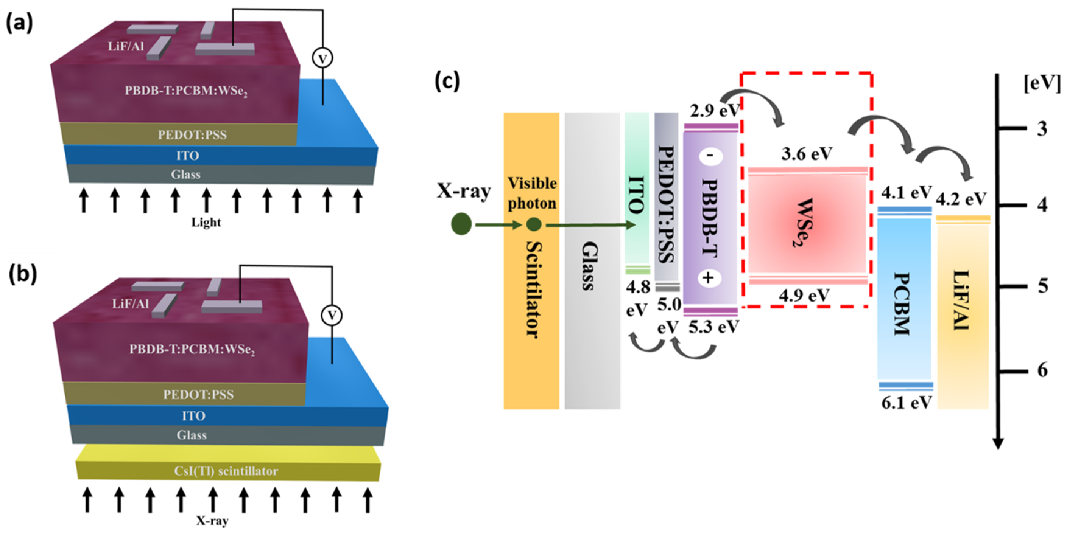
2. Experimental Section

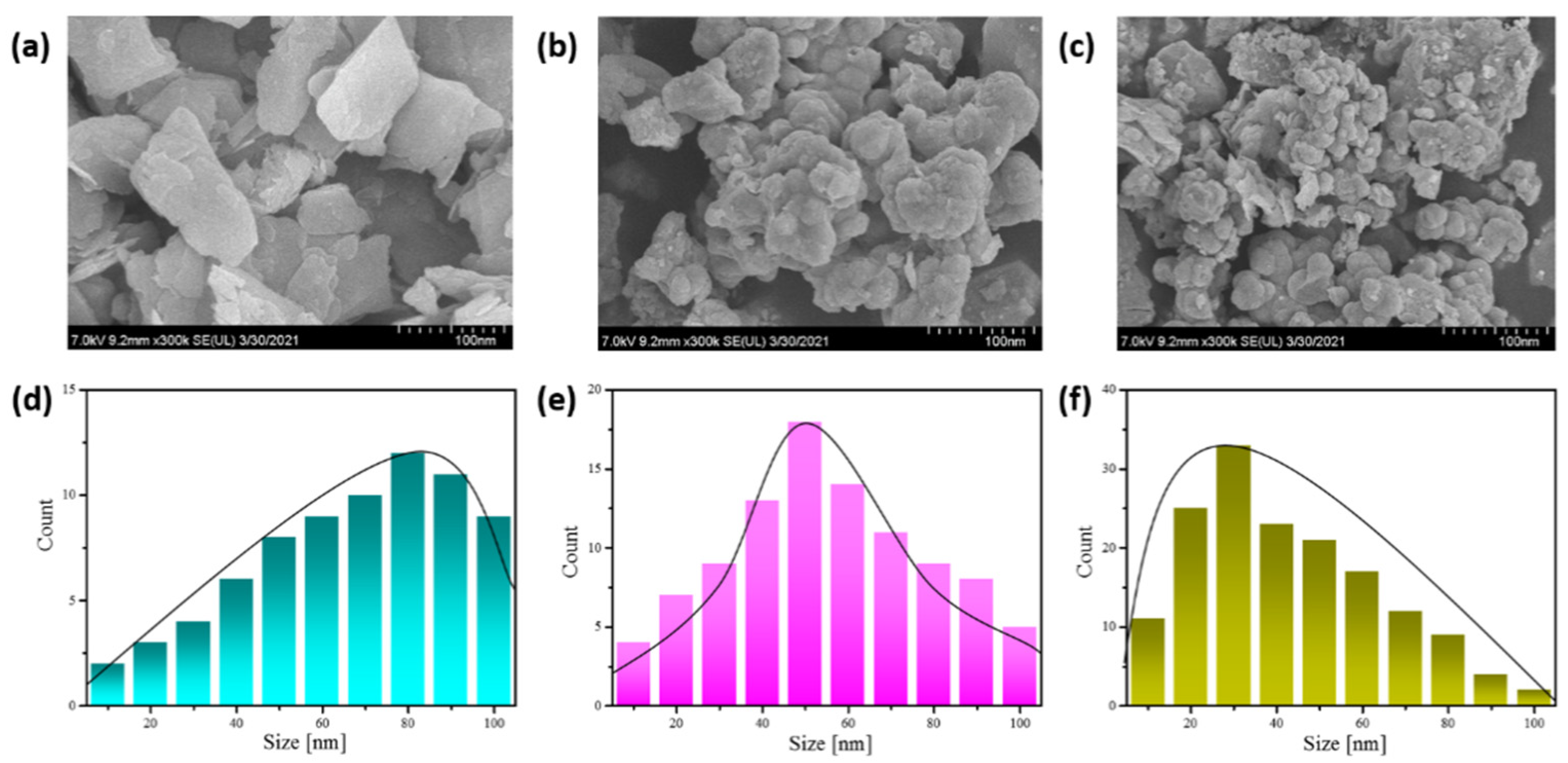
2.1. Preparation of WSe2 Nanosheets

Firstly, 1 g of WSe2 commercial powder was mixed with 100 mL of ethanol solution. The solution was then subjected to sonication at different times, such as 6, 12 and 18 h in a sonic bath under 60 W. Next, it was centrifuged at 8000 RPM for 5 min to retain the precipitate. The collected precipitate was then kept in a vacuum-heating oven until the ethanol evaporated. Finally, the prepared WSe2 nanosheets were used for device fabrication and characterization. Based on the sonication times of 6, 12 and 18 h for WSe2 preparation, the final products are named “NS1”, “NS2”, and “NS3”, respectively, in the following text. The WSe2 nanosheets’ ultrasonic preparation parameters are listed in Table S1 (Supplementary Materials).

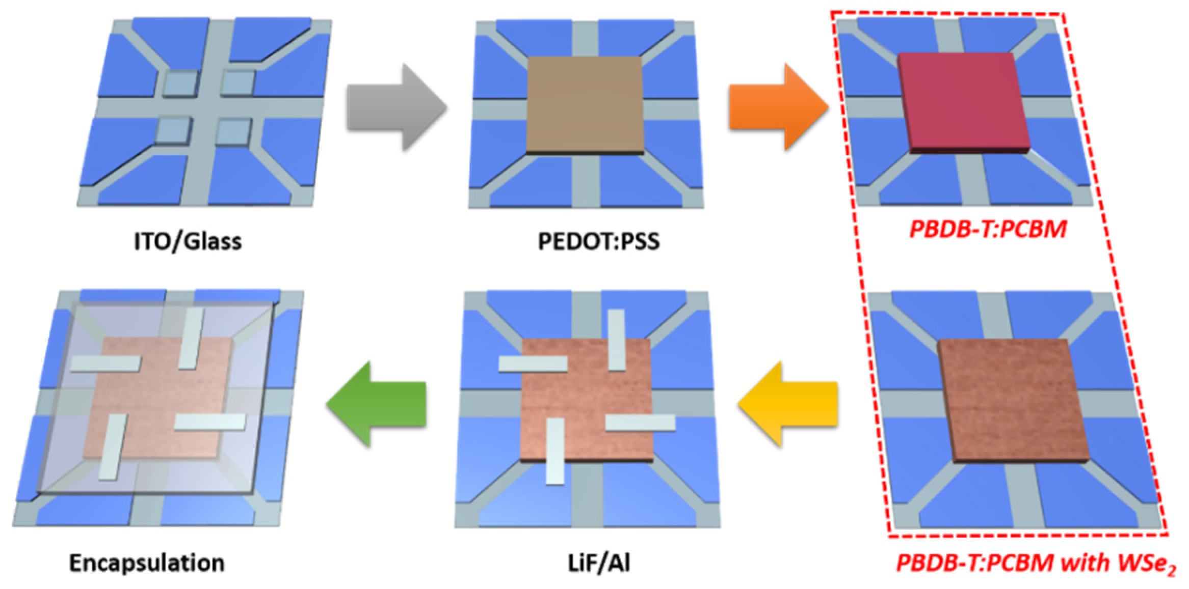
2.2. Device Fabrication

The indium tin oxide (ITO)-patterned glass substrates were cleaned sequentially with acetone, methanol, and isopropyl alcohol for 5 min by sonication treatment, then dried in a vacuum oven at 100 °C, before finally being exposed to UVO treatment for 15 min. The PEDOT:PSS was spin-coated onto the cleaned ITO substrate at 3000 rpm for 30 s and then annealed at 150 °C for 30 min, resulting in a 40 nm thick PEDOT:PSS. For the pure active layer formation, a mixture of PBDB-T and PCBM (with a weight ratio of 2:3) was completely dissolved in chlorobenzene with a concentration of 20 mg/mL, then subjected to constant stirring for 3 h at 60 °C. Next, the prepared solution was spin-coated onto the PEDOT:PSS layer at 1100 rpm for 30 s, and treated by thermal annealing at 150 °C for 10 min. To prepare the WSe2 NSs blended active layer, the selective concentration (1, 1.5, and 2 wt%) of prepared WSe2 NSs (NS1–NS3) was dissolved in isopropyl alcohol and then mixed with the chlorobenzene mixture (PBDB-T:PCBM—2:3 ratio), before being subjected to constant stirring for 3 h at 60 °C. The WSe2 NSs blended PBDB-T:PCBM active layer was then spin-coated onto the PEDOT:PSS layer at 1100 rpm for 30 s, and treated by thermal annealing at 150 °C for 10 min (Table S2). Finally, a 5 nm lithium fluoride (LiF) layer and a 120 nm Al cathode were deposited on top of the active layer by thermal evaporation under a pressurized environment of 3 × 10⁻⁷ torr. The fabricated device contains four cell structures with an active area of 0.04 cm2. To prevent the exposure of the fabricated detector to oxygen and humidity, it was enclosed under a glass lid in a glove box. The device fabrication scheme of a patterned ITO substrate with different active layers (PBDB-T:PCBM (92 nm) and PBDB-T:PCBM:WSe2 (89 nm)) is shown in Figure 1.

2.3. Characterization

Field emission scanning electron microscopy (FE-SEM, Hitachi S-4700, Tokyo, Japan) was used to describe the morphology and sizes of WSe2 NSs. Raman measurements were carried out using a Renishaw inVia (RE04, Gloucestershire, UK) spectrometer with a laser wavelength of 532 nm and an incident power of 5 mW for WSe2 NSs. The WSe2 NSs structural characteristics were characterized using in-plane X-ray diffraction (XRD, Rigaku D/Max-2500, Tokyo, Japan) with Cu-Kα radiation operated at 50 kV and 300 mA. Light absorption spectra were obtained using a UV–vis spectrophotometer (Optizen 2120UV, K LAB, Daejeon, Korea) for the pure and WSe2 NSs blended PBDB-T: PCBM active layers. Atomic force microscopy (AFM) measurements were obtained for the prepared active layers using Park Systems, XE-150 (Suwon, Korea), with a non-contact operating mode. The current density–voltage (J–V) characteristics of PSCs were measured with an electrometer (Keithley 6571B, Tektronix, Inc., Beaverton, OR, USA) under the exposure of an AM 1.5G-filtered Xe lamp with an intensity of 100 mW/cm2.
The X-ray detector combined with the scintillator was characterized under X-ray exposure. The emission spectrum of the CsI(Tl) scintillator (Hamamatsu Photonics J1311, Shizuoka, Japan) was measured under X-ray irradiation with a spectrometer (AvaSpec ULS2048L, StellarNet, Inc., Tampa, FL, USA). The prepared detector was placed at a distance of 30 cm from the X-ray generator, with the operation of the X-ray generator fixed under the conditions of 80 kVp and 60 mA·s, before being irradiated for 1.57 s. In order to collect the charge under the X-ray exposure period, a bias voltage of 0.6 V between the cathode and anode of the detector was applied. In addition, at the same distance (30 cm), the X-ray exposure dose was measured using an ion chamber (Capintec CII50, Mirion Technologies (Capintec), Inc., Florham Park, NJ, USA), and the absorbed dose from exposure to the X-ray was 3.14 mGy. The radiation parameters were calculated using the following Formulas (1) and (2), which correspond to the collected current density (CCD) under X-ray irradiation conditions and the dark current density (DCD) under X-ray irradiation conditions, respectively. The sensitivity of the X-ray detector was calculated using a Formula (3), which indicates that the current generated is proportional to the absorbed dose.
CCD   [ μ A cm 2 ] = Collected   Current   during   X-ray   ON Exposed   Detection   Area
DCD   [ μ A cm 2 ] = Collected   Current   during   X-ray   OFF Exposed   Detection   Area
Sensitivity   [ μ A mGy · cm 2 ] = CCD DCD Absorbed   Dose

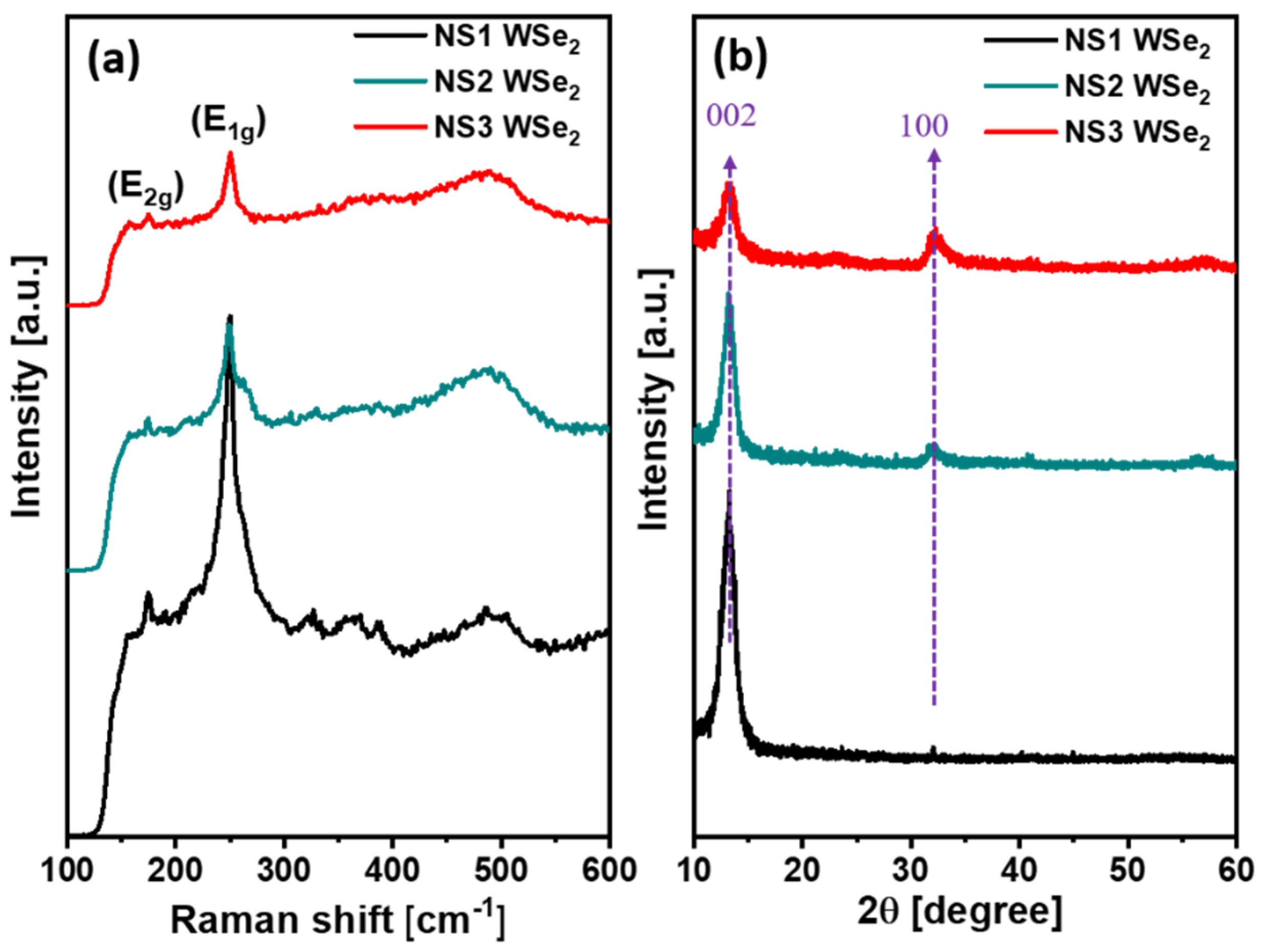
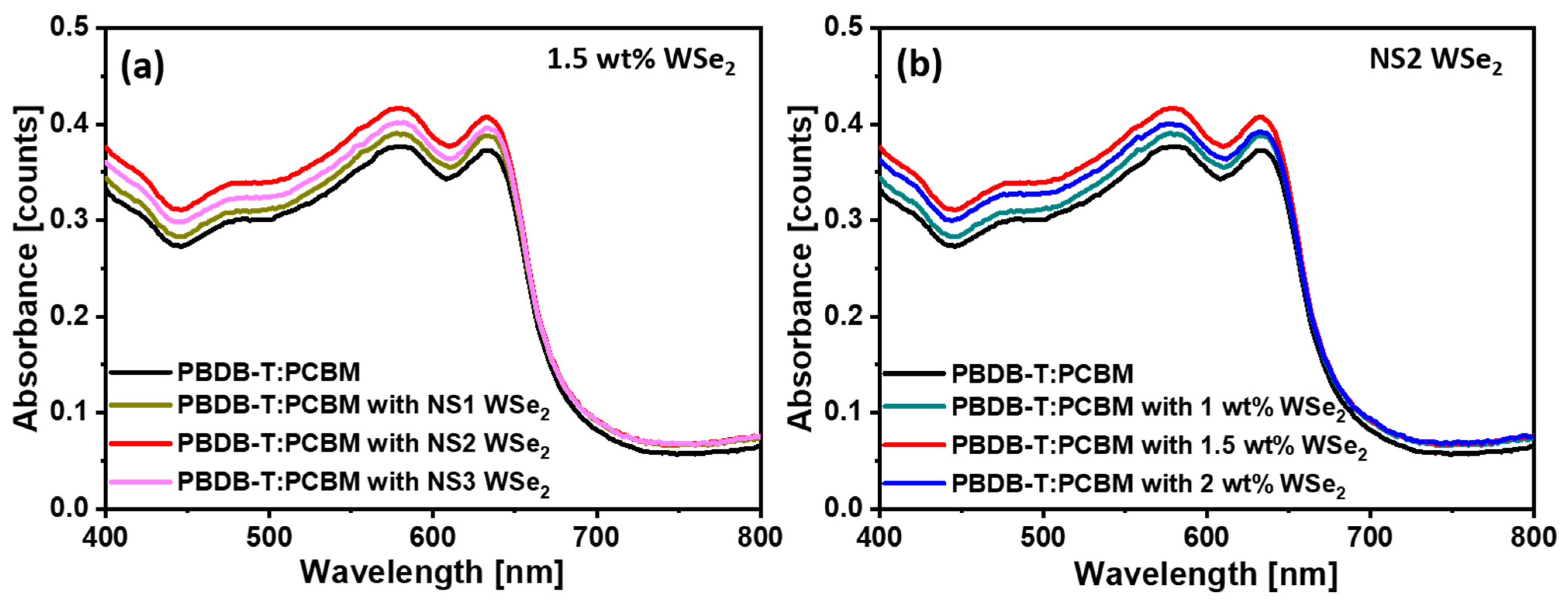
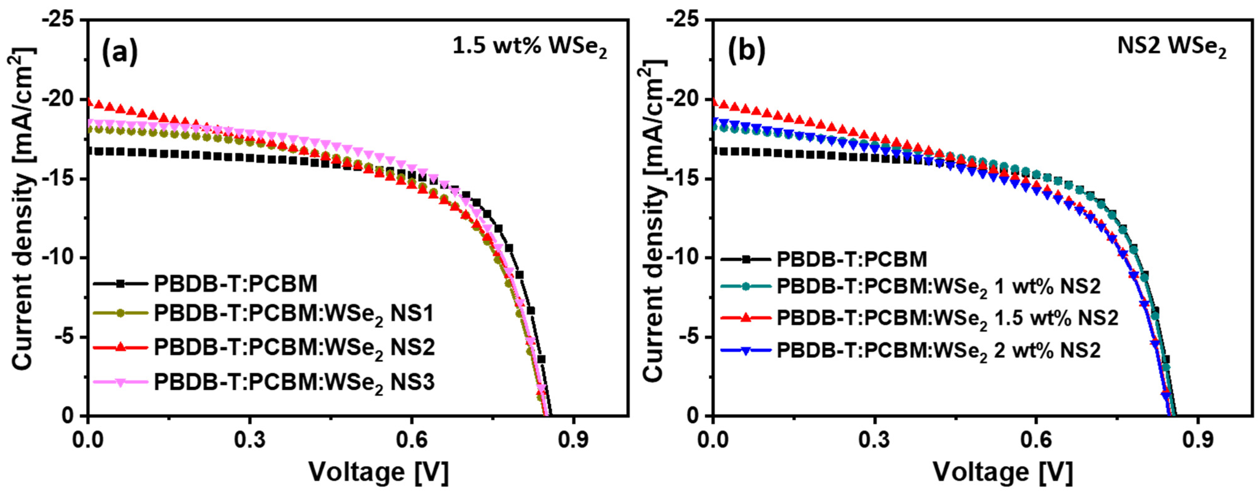
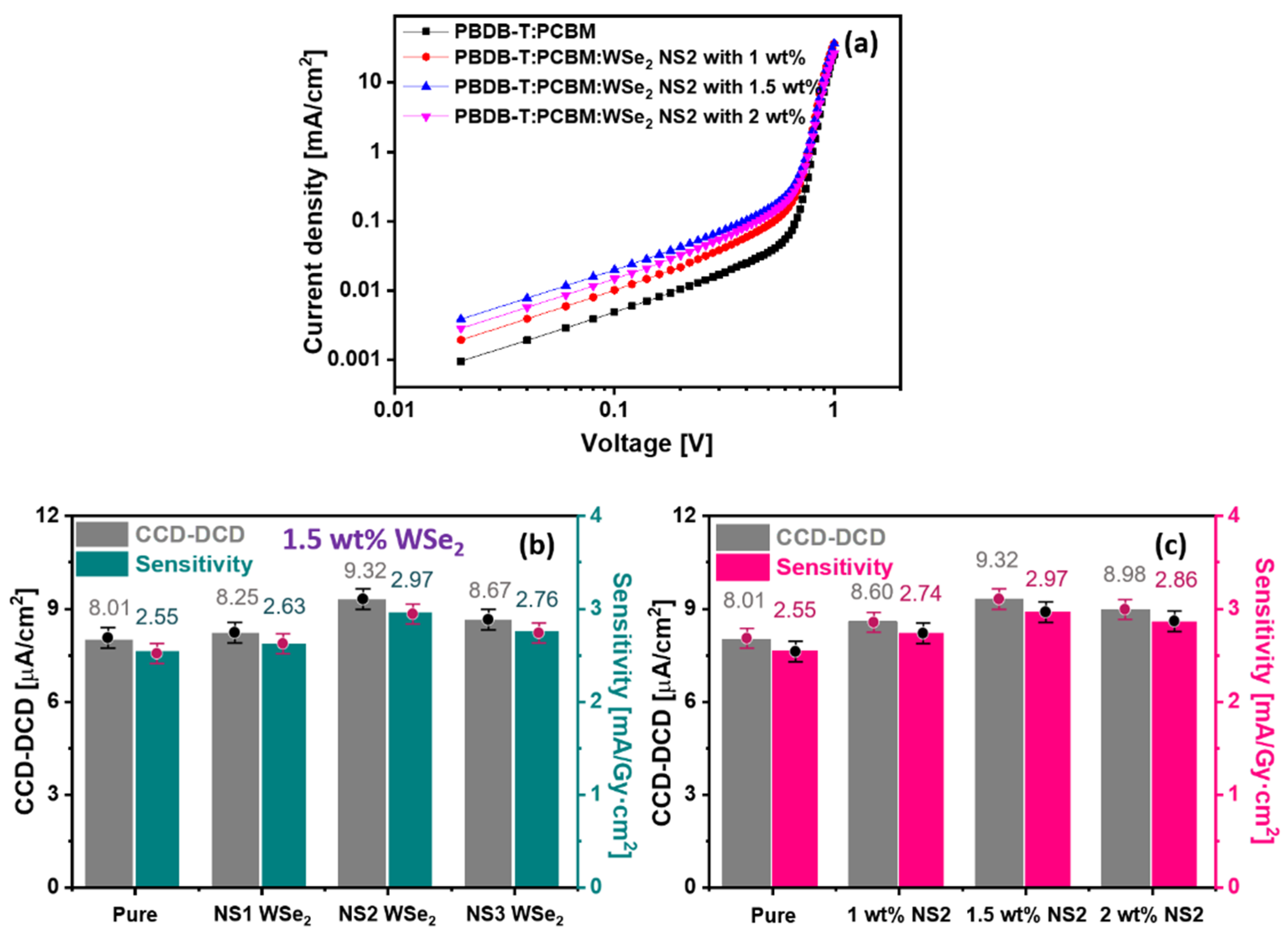
3. Results and Discussion

The morphological characteristics of different WSe2 NSs were evaluated by FE-SEM measurements. Figure 2a–c show the FE-SEM images of NS1, NS2 and NS3 WSe2, respectively. The prepared NS1 WSe2 produces the agglomerated larger-size granular structure with inhomogeneous shapes and sizes. Moreover, the observed surface reveals the voids and hillocks of a natured morphology. The sizes of the grains were estimated using line profiling with FE-SEM. The line profile of Figure 2d reveals NS1 WSe2 NSs with an average size of ~80 nm. Agglomerated grain bunches made of nano-sized grains are observed for NS2 WSe2 (Figure 2b). Furthermore, a line profile (Figure 2e) of NS2 WSe2 explores the ~50 nm diameter of average grain sizes. For NS3 WSe2, the fragmented sizes of differently shaped grains are shown in Figure 2c and its line profile (Figure 2f) indicates minimized sizes of grains with a ~30 nm average diameter. The observed results prove that the sizes of WSe2 NSs grains are purely affected by the time of ultrasonic treatment due to the dispersion of nanosheets during the ultrasonic treatment [50].
The structural property of NS1–NS3 WSe2 was characterized using Raman scattering analysis. Figure 3a shows the Raman scattering profiles of WSe2 NSs. The Raman scattering of NS1 displays two distinct characteristic peaks of E2g mode and E1g mode, located at 173.99 cm−1 and 250.22 cm−1, respectively [51,52]. For the NS2 and NS3 WSe2 nanostructures, the peak positions are kept constant but their peak intensities are considerably altered. In our observation, the Raman peak intensities reduced considerably after an increase in ultrasonic treatment. The layered structure of WSe2 bonded with weak Van der Waals forces between their layers. During the longer ultrasonic bath, weak forces collapsed and induced the agglomeration of the bulk nature of WSe2 [53]. In addition, due to the dispersion of the layered structure and nano-sheet sizes, the Raman phonon modes either significantly broadened or were strongly suppressed [52]. These agglomeration characteristics and size decrements are clearly portrayed in the Raman signals. The crystalline nature of NS1–NS3 WSe2 was characterized by XRD analysis. Figure 3b reveals the diffraction peaks of WSe2 located at 13.28° and 32.05° corresponding to the (002) and (100) lattice planes, respectively. The (002) peak intensity is significantly reduced, while the (100) plane intensity is considerably greater with an increase in sonication time [54,55]. The d-spacing of the (002) peak ascribes the single layer thickness of WSe2. After the lengthiest sonication of 18 h, the reduction in (002) peak intensity suggests the destacking/termination of the WSe2 layered architecture. The observed results are consistent with the Raman observation. However, unrelated layers randomly folded between other layers, resulting in an increase in (100) lattice-plane peak intensity. The observed results decoded the role of sonication time to produce the highly active WSe2 NSs.
The effect of incorporation of different WSe2 NSs with the PBDB-T:PCBM active layer on the optical properties was investigated by ultraviolet–visible absorption spectroscopy. Figure 4a shows the absorption spectra of pure and NS1–NS3 WSe2 NSs blended PBDB-T:PCBM film. The pristine PBDB-T:PCBM film’s absorption spectrum displays several characteristic features with the three distinct peaks at 474, 580 and 632 nm. An observed weak peak centered at 474 nm is associated with the absorption following the extended conjugation of PCBM in the solid state, and the doublets at 580 and 632 nm attribute to the interchain vibrational absorption of ordered PBDB-T chains. Compared to the pristine PBDB-T:PCBM, the PBDB-T:PCBM:WSe2 hybrid displays an enhancement in the absorption profile for different NS1–NS3 WSe2 (1.5 wt%), as shown in Figure 4a. Furthermore, the different concentrations, such as 1, 1.5 and 2 wt%, of NS2 WSe2 NSs blended PBDB-T:PCBM films’ absorption profiles are shown in Figure 4b, which depicts a high absorption behavior for the 1.5 wt% NS2 WSe2. The addition of WSe2 NSs with the PBDB-T:PCBM active layer provides a superior photon transmission path and enhances photon absorption characteristics.
The impact of the incorporation of WSe2 NSs with an active layer on the photovoltaic and photodetector performances of ITO/PEDOT:PSS/PBDB-T:PCBM:WSe2/LiF/Al device was measured by current density–voltage (J–V) characteristics. The schematic of the hybrid polymer solar cell’s structure and the X-ray detector’s structure is shown in Figure 5a,b, respectively. Figure 5c shows the energy level diagram of each component used for the fabrication of the device. For the X-ray detector, the CsI(Tl) scintillator was constructed, which consisted of 400 μm thick CsI and 0.5 mm thick Al. The induced X-ray photons were converted through the scintillator, and were then absorbed by the active layer (PBDB-T:PCBM:WSe2 NSs) to create electron–hole pairs. The transfer of electrons/holes through the cathode/anode thus collected charges. According to the energy band position, additive WSe2 NSs help the movement of electrons from PCBM to the cathode, whereas the hole transport layer (HTL) of PEDOT:PSS helps the movement of holes towards the anode.
To explore the photovoltaic behavior, the J–V characteristics of pristine PBDB-T:PCBM and WSe2 NSs-incorporated PBDB-T:PCBM devices were measured under AM 1.5 G conditions at an illumination intensity of 100 mW/cm2. Figure 6a shows the J–V characteristics of devices comprising pure and NS1–NS3 WSe2 NSs (1.5 wt%)-incorporated PBDB-T:PCBM active layers. Using a PSC device, we showed that the pristine PBDB-T:PCBM active layer displayed a short-circuit current density (Jsc) of 16.81 mA·cm2 and an open-circuit voltage (Voc) 0.84 V, with a fill factor (FF) of 56% and series resistance (Rs) of 225.43 Ω·cm2, resulting in a PCE of 8.1%. After the incorporation of different NS1–NS3 WSe2 NSs, the performances of the PSC devices were considerably improved. Further, the observed PSC outcomes are provided in Table 1. After the incorporation of WSe2 NSs into the active layer, the light-absorption capacity of the composite films significantly improved compared to the pristine device, which promoted the exciton generation rate. The results reveal that the device with the NS2 (1.5 wt%) WSe2 NSs active layer produces the highest JSC of 19.78 mA/cm2, VOC of 0.85 V, Rs of 122.02 Ω·cm2 and FF of 55%, with a very promising PCE of 9.2%. The presence of WSe2 NSs in the ternary blend provides an additional PBDB-T:PCBM:WSe2 interface, thus inducing a large interfacial area for charge separation, and it thereby accelerates the rate of exciton dissociation. Moreover, the highly conductive 2D network of NS2 WSe2 NSs offers new interconnected percolation networks for charge-carrier transport and collection, which could improve the electron mobility, resulting in larger JSC. The observed low Rs further establishes the improved solar cell performances for WSe2-incorporating active layers. The observed values are provided with standard deviation (Table 1) between their five replicated experiments to prove their stable performances. Similarly, the J–V characteristics of the constructed devices using different concentrations, such as 1, 1.5 and 2 wt%, of NS2 WSe2 blended PBDB-T:PCBM:WSe2 in their active layer are provided in Figure 6b. The observed results clearly illustrate the improved behavior of the 1.5 wt% blended active layers. The detailed PSC parameters are presented in the Table 2. In addition, in order to realize the role of concentration variation in achieving high performance, AFM measurements were performed to study the topography of the active layer prepared on ITO-coated glass. Figure S1 shows the 3D AFM topographical images of pure and different concentrations (1, 1.5 and 2 wt%) of the NS2 WSe2-doped PBDB-T:PCBM heterojunction active layer. The RMS surface roughness of the active layer is 1.73 nm, 1.59 nm, 1.49 nm and 1.53 nm for the pure and 1, 1.5 and 2 wt% NS2 WSe2-doped PBDB-T:PCBM active layers, respectively. The development of a very dense PCDTB-T:PCBM:WSe2 NS2 (1.5 wt%) active layer could prevent the leakage of current and produce conduits useful for charge conveyance and separation, improving the device’s performance [56]. Further, to validate the performances of the devices with different concentrations (1, 1.5, and 2 wt%) of NS1 and NS3 WSe2 doping, PSC J–V profiles are provided in Figures S2 and S3, respectively.
The fabricated X-ray detectors were measured using the X-ray generator and electrometer, as described in the experimental part. Figure 7a shows the logarithmic J–V characteristics of pure and NS1–NS3 WSe2 NSs (1.5 wt%) blended PBDB-T:PCBM active layers using prepared detectors. For the pristine PBDB-T:PCBM active layer, the X-ray detector achieves a 2.55 mA/Gy·cm2 sensitivity. When the active layer is blended with NS1–NS3 WSe2 NSs, the sensitivity is increased to 2.63, 2.97, and 2.76 mA/Gy·cm2 for NS1, NS2 and NS3, respectively (Figure 7b, right-side axis). The extracted CCD-DCDs (Figure 7b, left side axis) are at 8.01, 8.25, 9.32, and 8.67 μA/cm2 for the pure and NS1–NS3 blended PBDB-T:PCBM active layers using the prepared X-ray detectors, respectively. Similarly, the outcomes of different NS2 WSe2 NSs blended PBDB-T:PCBM active layers using prepared X-ray detectors are provided in Figure 7c. The sensitivity as assessed by X-ray realizes gives values of 2.55, 2.74, 2.97, and 2.86 mA/Gy·cm2 for the pristine PBDB-T:PCBM active layer and 1 wt%, 1.5 wt% and 2 wt% NS2 WSe2 NSs, respectively (as shown in Figure 7c, right-side axis). The estimated CCD-DCD values are 8.01, 8.60, 9.32, and 8.98 μA/cm2 for the pristine PBDB-T:PCBM active layer and 1 wt%, 1.5 wt% and 2 wt% NS2 WSe2 NSs, respectively. The observed X-ray detector outcomes for NS1 and NS3 WSe2 NSs (1, 1.5, and 2 wt%) blended PBDB-T:PCBM active layers are provided in Figures S3 and S4, respectively. Better outcomes are ensured for the 1.5 wt% NS2 WSe2 NSs hybrid active layer under X-ray detection due to the enhanced conductivity, improved light absorption capacity, and superior mobility.
The carrier mobility was determined using the space-charge-limited-current (SCLC) method in the dark, and it was obtained using the modified Mott–Gurney equation as shown below:
μ = 8 9 × J × L 3 V a 2 × ε 0 × ε r
where ε0 is the permittivity of free space (=8.85 × 10⁻¹² F·m−1), εr is the relative permittivity of the active layer, Va is the voltage applied across the detector, μ is the carrier mobility, and L is the thickness of the active layer. The calculated mobilities using the detector are at 5.62 × 10⁻⁵, 5.23 × 10⁻⁴, 8.82 × 10⁻⁴, and 7.13 × 10⁻⁴ cm2/V·s for the pristine active layer and 1 wt%, 1.5 wt% and 2 wt% of NS2 WSe2 NSs blended active layers, respectively.

4. Conclusions

In this work, we have ultrasonically prepared exfoliated WSe2 NSs and blended them with PBDB-T:PCBM as an active layer for ternary hybrid solar cells and X-ray detectors. The different types (NS1–NS3) of WSe2 NSs were incorporated with active layers to explore their potentials to alter the electron transport behavior in the prepared devices. The TMD WSe2 blended active layer produced a synergistic enhancement of exciton generation and dissociation, and enhanced hole and electron transport through the active layer, which helped in achieving the high JSC and PCE for solar cells and the high sensitivity of detectors. The highest PCE of 9.2% was attained for the NS2 WSe2 (1.5 wt%) blended PBDB-T:PCBM active layer, which is higher than the devices comprised of pristine and NS1 and NS3 blended active layers. The fabricated X-ray detectors achieved the maximum CCD-DCD of 9.32 μA/cm2, a high sensitivity of 2.97 mA/Gy·cm2, and large carrier mobility of 8.82 × 10⁻⁴ cm2/V·s for the NS2 WSe2 (1.5 wt%) blended PBDB-T:PCBM active layer. Our research work provides a good strategy for incorporating highly dispersed aggregated WSe2 NSs in an active layer to promote the charge extraction process and electron/hole transport behavior, thus realizing high-performance semiconductor devices. These results offer a new direction for the development of high-performance devices based on hybrid structures for future electronics.

Supplementary Materials

The following are available online at https://www.mdpi.com/article/10.3390/ma14123206/s1, Table S1: Ultrasonic preparation parameters for WSe2 nanosheets. Table S2: Active layer preparation parameters. Figure S1. Atomic force measurement (AFM) image (a) PBDB-T:PCBM, (b) PBDB-T:PCBM:WSe2NS2 with 1 wt%, (c) PBDB-T:PCBM:WSe2 NS2 with 1.5 wt% and (d) PBDB-T:PCBM:WSe2 NS2 with 2 wt%, Figure S2: J–V characteristics and their outcomes for pristine and different amounts NS1 WSe2 NSs blended PBDB-T:PCBM active layer, Figure S3: J–V characteristics and their outcomes for pristine and different amounts NS3 WSe2 NSs blended PBDB-T:PCBM active layer, Figure S4: CCD-DCD and sensitivity variations for pure and different concentrations of NS1 WSe2 NSs blended PBDB-T:PCBM active layer comprised X-ray detectors, Figure S5: CCD-DCD and sensitivity variations for pure and different concentrations of NS3 WSe2 NSs blended PBDB-T:PCBM active layer comprised X-ray detectors, Table S3: Photovoltaic parameters of polymer/2D materials–based PSCs.

Author Contributions

Conceptualization, H.L. and S.H.; data curation, J.L.; formal analysis, H.L., S.H. and J.L.; funding acquisition, J.K.; investigation, S.H. and D.V.; methodology, H.L. and D.V.; software, J.L.; supervision, J.K.; validation, D.V.; writing—original draft, H.L. and S.H.; writing—review and editing, D.V. and J.K. All authors have read and agreed to the published version of the manuscript.

Funding

This work was supported by the National Research Foundation of Korea (NRF) grant funded by the Korea government (MSIT) (No. 2017R1A2A2A05069821).

Institutional Review Board Statement

Not applicable.

Informed Consent Statement

Not applicable.

Data Availability Statement

Data Sharing is not applicable.

Conflicts of Interest

The authors declare no conflict of interest.

References

  1. Foster, S.; Deledalle, F.; Mitani, A.; Kimura, T.; Kim, K.-B.; Okachi, T.; Kirchartz, T.; Oguma, J.; Miyake, K.; Durrant, J.R.; et al. Electron Collection as a Limit to Polymer:PCBM Solar Cell Efficiency: Effect of Blend Microstructure on Carrier Mobility and Device Performance in PTB7:PCBM. Adv. Energy Mater. 2014, 4, 1400311. [Google Scholar] [CrossRef]
  2. Oh, S.H.; Heo, S.J.; Yang, J.S.; Kim, H.J. Effects of ZnO Nanoparticles on P3HT:PCBM Organic Solar Cells with DMF-Modulated PEDOT:PSS Buffer Layers. ACS Appl. Mater. Interfaces 2013, 5, 11530–11534. [Google Scholar] [CrossRef]
  3. Xu, Y.; Yuan, J.; Zhou, S.; Seifrid, M.; Ying, L.; Li, B.; Huang, F.; Bazan, G.C.; Ma, W. Ambient Processable and Stable All-Polymer Organic Solar Cells. Adv. Funct. Mater. 2019, 29, 1806747. [Google Scholar] [CrossRef]
  4. Lee, D.; Kim, J.; Park, G.; Bae, H.W.; An, M.; Kim, J.Y. Enhanced Operating Temperature Stability of Organic Solar Cells with Metal Oxide Hole Extraction Layer. Polymers 2020, 12, 992. [Google Scholar] [CrossRef] [PubMed]
  5. Zhang, Q.; Li, B.; Huang, S.; Nomura, H.; Tanaka, H.; Adachi, C. Efficient blue organic light-emitting diodes employing thermally activated delayed fluorescence. Nat. Photon. 2014, 8, 326–332. [Google Scholar] [CrossRef]
  6. Huang, T.; Jiang, W.; Duan, L. Recent progress in solution processable TADF materials for organic light-emitting diodes. J. Mater. Chem. C 2018, 6, 5577–5596. [Google Scholar] [CrossRef]
  7. Torsi, L.; Magliulo, M.; Manoli, K.; Palazzo, G. Organic field-effect transistor sensors: A tutorial review. Chem. Soc. Rev. 2013, 42, 8612–8628. [Google Scholar] [CrossRef] [PubMed]
  8. Lee, Y.H.; Kweon, O.Y.; Kim, H.; Yoo, J.H.; Han, S.G.; Oh, J.H. Recent advances in organic sensors for health self-monitoring systems. J. Mater. Chem. C 2018, 6, 8569–8612. [Google Scholar] [CrossRef]
  9. Wang, W.; Zhang, F.; Du, M.; Li, L.; Zhang, M.; Wang, K.; Wang, Y.; Hu, B.; Fang, Y.; Huang, J. Highly Narrowband Photomultiplication Type Organic Photodetectors. Nano Lett. 2017, 17, 1995–2002. [Google Scholar] [CrossRef]
  10. Yang, D.; Ma, D. Development of Organic Semiconductor Photodetectors: From Mechanism to Applications. Adv. Opt. Mater. 2019, 7, 1800522. [Google Scholar] [CrossRef]
  11. Fujisaki, Y.; Koga, H.; Nakajima, Y.; Nakata, M.; Tsuji, H.; Yamamoto, T.; Kurita, T.; Nogi, M.; Shimidzu, N. Transparent Nanopaper-Based Flexible Organic Thin-Film Transistor Array. Adv. Funct. Mater. 2014, 24, 1657–1663. [Google Scholar] [CrossRef]
  12. Kaltenbrunner, M.; White, M.S.; Głowacki, E.D.; Sekitani, T.; Someya, T.; Sariciftci, N.S.; Bauer, S. Ultrathin and lightweight organic solar cells with high flexibility. Nat. Commun. 2012, 3, 770. [Google Scholar] [CrossRef] [Green Version]
  13. Han, J.; Bao, F.; Huang, D.; Wang, X.; Yang, C.; Yang, R.; Jian, X.; Wang, J.; Bao, X.; Chu, J. A Universal Method to Enhance Flexibility and Stability of Organic Solar Cells by Constructing Insulating Matrices in Active Layers. Adv. Funct. Mater. 2020, 30, 2003654. [Google Scholar] [CrossRef]
  14. Howarth, A.J.; Liu, Y.; Li, P.; Li, Z.; Wang, T.C.; Hupp, J.T.; Farha, O.K. Chemical, thermal and mechanical stabilities of metal–organic frameworks. Nat. Rev. Mater. 2016, 1, 15018. [Google Scholar] [CrossRef]
  15. Zhou, K.; Xin, J.; Ma, W. Hierarchical Morphology Stability under Multiple Stresses in Organic Solar Cells. ACS Energy Lett. 2019, 4, 447–455. [Google Scholar] [CrossRef]
  16. Zamani-Meymian, M.-R.; Sheikholeslami, S.; Fallah, M. Stability of Non-Flexible vs. Flexible Inverted Bulk-Heterojunction Organic Solar Cells with ZnO as Electron Transport Layer Prepared by a Sol-Gel Spin Coating Method. Surfaces 2020, 3, 319–327. [Google Scholar] [CrossRef]
  17. Mousavi, S.L.; Jamali-Sheini, F.; Sabaeian, M.; Yousefi, R. Enhanced solar cell performance of P3HT:PCBM by SnS nanoparticles. Sol. Energy 2020, 199, 872–884. [Google Scholar] [CrossRef]
  18. Krantz, J.; Stubhan, T.; Richter, M.; Spallek, S.; Litzov, I.; Matt, G.J.; Spiecker, E.; Brabec, C.J. Spray-Coated Silver Nanowires as Top Electrode Layer in Semitransparent P3HT:PCBM-Based Organic Solar Cell Devices. Adv. Funct. Mater. 2012, 23, 1711–1717. [Google Scholar] [CrossRef]
  19. Liu, F.; Chen, D.; Wang, C.; Luo, K.; Gu, W.; Briseno, A.L.; Hsu, J.W.P.; Russell, T.P. Molecular Weight Dependence of the Morphology in P3HT:PCBM Solar Cells. ACS Appl. Mater. Interfaces 2014, 6, 19876–19887. [Google Scholar] [CrossRef] [PubMed]
  20. Abdallaoui, M.; Sengouga, N.; Chala, A.; Meftah, A. Comparative study of conventional and inverted P3HT: PCBM organic solar cell. Opt. Mater. 2020, 105, 109916. [Google Scholar] [CrossRef]
  21. Lee, J.; Liu, H.; Kang, J. A Study on an Organic Semiconductor-Based Indirect X-ray Detector with Cd-Free QDs for Sensitivity Improvement. Sensors 2020, 20, 6562. [Google Scholar] [CrossRef]
  22. Bellani, S.; Najafi, L.; Capasso, A.; Castillo, A.E.D.R.; Antognazza, M.R.; Bonaccorso, F. Few-layer MoS2 flakes as a hole-selective layer for solution-processed hybrid organic hydrogen-evolving photocathodes. J. Mater. Chem. A 2017, 5, 4384–4396. [Google Scholar] [CrossRef] [Green Version]
  23. Li, S.; Ye, L.; Zhao, W.; Yan, H.; Yang, B.; Liu, D.; Li, W.; Ade, H.; Hou, J. A Wide Band Gap Polymer with a Deep Highest Occupied Molecular Orbital Level Enables 14.2% Efficiency in Polymer Solar Cells. J. Am. Chem. Soc. 2018, 140, 7159–7167. [Google Scholar] [CrossRef]
  24. Li, X.; Ma, R.; Liu, T.; Xiao, Y.; Chai, G.; Lu, X.; Yan, H.; Li, Y. Fine-tuning HOMO energy levels between PM6 and PBDB-T polymer donors via ternary copolymerization. Sci. China Ser. B Chem. 2020, 63, 1256–1261. [Google Scholar] [CrossRef]
  25. Gloeckler, M.; Sankin, I.; Zhao, Z. CdTe Solar Cells at the Threshold to 20 Efficiency. IEEE J. Photovolt. 2013, 3, 1389–1393. [Google Scholar] [CrossRef]
  26. Mariani, G.; Scofield, A.C.; Hung, C.-H.; Huffaker, D.L. GaAs nanopillar-array solar cells employing in situ surface passivation. Nat. Commun. 2013, 4, 1497. [Google Scholar] [CrossRef] [PubMed] [Green Version]
  27. Zhang, Y.; Bartolo, R.E.; Kwon, S.J.; Dagenais, M. High Short-Circuit Current Density in CIS Solar Cells by a Simple Two-Step Selenization Process With a KF Postdeposition Treatment. IEEE J. Photovolt. 2016, 7, 1–8. [Google Scholar] [CrossRef]
  28. Mufti, N.; Amrillah, T.; Taufiq, A.; Sunaryono, A.; Diantoro, M.; Zulhadjri, N.H. Review of CIGS-based solar cells manufacturing by structural engineering. Sol. Energy 2020, 207, 1146–1157. [Google Scholar] [CrossRef]
  29. Li, P.; Wu, B.; Yang, Y.C.; Huang, H.S.; De Yang, X.; Zhou, G.D.; Song, Q.L. Improved charge transport ability of polymer solar cells by using NPB/MoO3 as anode buffer layer. Sol. Energy 2018, 170, 212–216. [Google Scholar] [CrossRef]
  30. Sygletou, M.; Tzourmpakis, P.; Petridis, C.; Konios, D.; Fotakis, C.; Kymakis, E.; Stratakis, E. Laser induced nucleation of plasmonic nanoparticles on two-dimensional nanosheets for organic photovoltaics. J. Mater. Chem. A 2016, 4, 1020–1027. [Google Scholar] [CrossRef]
  31. Wu, W.; Wu, H.; Zhong, M.; Guo, S. Dual Role of Graphene Quantum Dots in Active Layer of Inverted Bulk Heterojunction Organic Photovoltaic Devices. ACS Omega 2019, 4, 16159–16165. [Google Scholar] [CrossRef] [PubMed] [Green Version]
  32. Ahmad, R.; Srivastava, R.; Yadav, S.; Chand, S.; Sapra, S. Functionalized 2D-MoS2-incorporated polymer ternary solar cells: Role of nanosheet-induced long-range ordering of polymer chains on charge transport. ACS Appl. Mater. Interfaces 2017, 9, 34111–34121. [Google Scholar] [CrossRef] [PubMed]
  33. Ameri, T.; Khoram, P.; Min, J.; Brabec, C.J. Organic Ternary Solar Cells: A Review. Adv. Mater. 2013, 25, 4245–4266. [Google Scholar] [CrossRef]
  34. Dwivedi, S.K.; Tiwari, D.; Tripathi, S.K.; Dwivedi, P.K.; Dipak, P.; Chandel, T.; Prasad, N.E. Fabrication and properties of P3HT: PCBM/Cu2SnSe3 (CTSe) nanocrystals based inverted hybrid solar cells. Sol. Energy 2019, 187, 167–174. [Google Scholar] [CrossRef]
  35. Panwar, H.; Gupta, P.; Siddiqui, M.K.; Morales-Menendez, R.; Singh, V. Application of deep learning for fast detection of COVID-19 in X-Rays using nCOVnet. Chaos Solitons Fractals 2020, 138, 109944. [Google Scholar] [CrossRef]
  36. Mathanker, S.K.; Weckler, P.R.; Bowser, T.J. X-Ray Applications in Food and Agriculture: A Review. Trans. ASABE 2013, 56, 1227–1239. [Google Scholar] [CrossRef]
  37. Thomas, J.M. The birth of X-ray crystallography. Nature 2012, 491, 186–187. [Google Scholar] [CrossRef] [PubMed]
  38. Woińska, M.; Grabowsky, S.; Dominiak, P.; Woźniak, K.; Jayatilaka, D. Hydrogen atoms can be located accurately and precisely by x-ray crystallography. Sci. Adv. 2016, 2, e1600192. [Google Scholar] [CrossRef] [Green Version]
  39. Vikraman, D.; Liu, H.; Hussain, S.; Karuppasamy, K.; Youi, H.-K.; Jung, J.; Kang, J.; Kim, H.-S. Influence of morphological tuned nanostructure hybrid layers on efficient bulk heterojunction organic solar cell and X-ray detector performances. Appl. Surf. Sci. 2021, 543, 148863. [Google Scholar] [CrossRef]
  40. Xu, Y.; Zhou, Q.; Huang, J.; Li, W.; Chen, J.; Wang, K. Highly-Sensitive Indirect-Conversion X-Ray Detector With an Embedded Photodiode Formed by a Three-Dimensional Dual-Gate Thin-Film Transistor. J. Light. Technol. 2020, 38, 3775–3780. [Google Scholar] [CrossRef]
  41. Thirimanne, H.M.; Jayawardena, K.D.G.I.; Parnell, A.J.; Bandara, R.M.I.; Karalasingam, A.; Pani, S.; Huerdler, J.E.; Lidzey, D.G.; Tedde, S.F.; Nisbet, A.; et al. High sensitivity organic inorganic hybrid X-ray detectors with direct transduction and broadband response. Nat. Commun. 2018, 9, 1–10. [Google Scholar] [CrossRef] [PubMed]
  42. Vikraman, D.; Hussain, S.; Rabani, I.; Feroze, A.; Ali, M.; Seo, Y.-S.; Chun, S.-H.; Jung, J.; Kim, H.-S. Engineering MoTe2 and Janus SeMoTe nanosheet structures: First-principles roadmap and practical uses in hydrogen evolution reactions and symmetric supercapacitors. Nano Energy 2021, 87, 106161. [Google Scholar] [CrossRef]
  43. Liu, H.; Hussain, S.; Ali, A.; Naqvi, B.A.; Vikraman, D.; Jeong, W.; Song, W.; An, K.-S.; Jung, J. A vertical WSe2–MoSe2 p–n heterostructure with tunable gate rectification. RSC Adv. 2018, 8, 25514–25518. [Google Scholar] [CrossRef] [Green Version]
  44. Nguyen, D.A.; Oh, H.M.; Duong, N.T.; Bang, S.H.; Yoon, S.J.; Jeong, M.S. Highly Enhanced Photoresponsivity of a Monolayer WSe2 Photodetector with Nitrogen-Doped Graphene Quantum Dots. ACS Appl. Mater. Interfaces 2018, 10, 10322–10329. [Google Scholar] [CrossRef]
  45. Ji, H.G.; Solís-Fernández, P.; Yoshimura, D.; Maruyama, M.; Endo, T.; Miyata, Y.; Okada, S.; Ago, H. Chemically Tuned p-and n-Type WSe2 Monolayers with High Carrier Mobility for Advanced Electronics. Adv. Mater. 2019, 31, 1903613. [Google Scholar] [CrossRef]
  46. Vikraman, D.; Hussain, S.; Patil, S.A.; Truong, L.; Arbab, A.A.; Jeong, S.H.; Chun, S.-H.; Jung, J.; Kim, H.-S. Engineering MoSe2/WS2 Hybrids to Replace the Scarce Platinum Electrode for Hydrogen Evolution Reactions and Dye-Sensitized Solar Cells. ACS Appl. Mater. Interfaces 2021, 13, 5061–5072. [Google Scholar] [CrossRef]
  47. Vikraman, D.; Akbar, K.; Hussain, S.; Yoo, G.; Jang, J.-Y.; Chun, S.-H.; Jung, J.; Park, H.J. Direct synthesis of thickness-tunable MoS2 quantum dot thin layers: Optical, structural and electrical properties and their application to hydrogen evolution. Nano Energy 2017, 35, 101–114. [Google Scholar] [CrossRef]
  48. Su, Y.-W.; Lin, Y.-C.; Wei, K.-H. Evolving molecular architectures of donor–acceptor conjugated polymers for photovoltaic applications: From one-dimensional to branched to two-dimensional structures. J. Mater. Chem. A 2017, 5, 24051–24075. [Google Scholar] [CrossRef]
  49. Liu, H.; Hussain, S.; Kang, J. Improvement in sensitivity of an indirect-type organic X-ray detector using an amorphous IGZO interfacial layer. J. Instrum. 2020, 15, P02002. [Google Scholar] [CrossRef]
  50. Zhang, B.; Chen, T. Study of Ultrasonic Dispersion of Graphene Nanoplatelets. Materials 2019, 12, 1757. [Google Scholar] [CrossRef] [Green Version]
  51. Hussain, S.; Patil, S.A.; Vikraman, D.; Arbab, A.A.; Jeong, S.H.; Kim, H.-S.; Jung, J. Growth of a WSe2/W counter electrode by sputtering and selenization annealing for high-efficiency dye-sensitized solar cells. Appl. Surf. Sci. 2017, 406, 84–90. [Google Scholar] [CrossRef]
  52. Li, H.; Lu, G.; Wang, Y.; Yin, Z.; Cong, C.; He, Q.; Wang, L.; Ding, F.; Yu, T.; Zhang, H. Mechanical exfoliation and characterization of single-and few-layer nanosheets of WSe2, TaS2, and TaSe2. Small 2013, 9, 1974–1981. [Google Scholar] [CrossRef] [PubMed]
  53. Hussain, S.; Akbar, K.; Vikraman, D.; Afzal, R.A.; Song, W.; An, K.-S.; Farooq, A.; Park, J.-Y.; Chun, S.-H.; Jung, J. WS(1−x)Sex Nanoparticles Decorated Three-Dimensional Graphene on Nickel Foam: A Robust and Highly Efficient Electrocatalyst for the Hydrogen Evolution Reaction. Nanomaterials 2018, 8, 929. [Google Scholar] [CrossRef] [Green Version]
  54. Panigrahi, P.K.; Pathak, A. A novel route for the synthesis of nanotubes and fullerene-like nanostructures of molybdenum disulfide. Mater. Res. Bull. 2011, 46, 2240–2246. [Google Scholar] [CrossRef]
  55. Tan, X.; Kang, W.; Liu, J.; Zhang, C. Synergistic Exfoliation of MoS2 by Ultrasound Sonication in a Supercritical Fluid Based Complex Solvent. Nanoscale Res. Lett. 2019, 14, 1–7. [Google Scholar] [CrossRef] [PubMed]
  56. Kakavelakis, G.; Castillo, A.E.D.R.; Pellegrini, V.; Ansaldo, A.; Tzourmpakis, P.; Brescia, R.; Prato, M.; Stratakis, E.; Kymakis, E.; Bonaccorso, F. Size-Tuning of WSe2 Flakes for High Efficiency Inverted Organic Solar Cells. ACS Nano 2017, 11, 3517–3531. [Google Scholar] [CrossRef] [PubMed]
Figure 1. Schematic process for the fabrication of pure and WSe2 NSs-suspended PBDB-T:PCBM active layer comprising a BHJ device.
Materials 14 03206 g001
Figure 2. SEM images of WSe2 NSs (a) NS1 (6 h sonication), (b) NS2 (12 h sonication), and (c) NS3 (18 h sonication); (df) particle size distribution of WSe2 NSs (d) NS1 (6 h sonication), (e) NS2 (12 h sonication) and (f) NS3 (18 h sonication).
Materials 14 03206 g002
Figure 3. (a) Raman spectra and (b) XRD patterns of NS1–NS3 WSe2 NSs.
Materials 14 03206 g003
Figure 4. (a) UV–vis absorption spectra of pure and NS1–NS3 WSe2 NSs blended PBDB-T:PCBM film; (b) UV–vis absorption spectra of pure and different concentrations of NS2 WSe2 blended PBDB-T:PCBM film.
Materials 14 03206 g004
Figure 5. Schematic illustration of (a) hybrid polymer solar cell structure; (b) X-ray detector structure combined with ScI(Tl) scintillator; (c) energy level diagram of the device.
Materials 14 03206 g005
Figure 6. J–V characteristics: (a) pristine and different WSe2 NSs blended PBDB-T:PCBM active layers; (b) pristine and different amounts of NS2 WSe2 NSs blended into the PBDB-T:PCBM active layer.
Materials 14 03206 g006
Figure 7. (a) Log J–V characteristics and (b) CCD-DCD and sensitivity variations (with the standard deviation error bar) Figure S1. NS3 WSe2 NSs blended PBDB-T:PCBM active layers as assessed by X-ray detectors; (c) CCD-DCD and sensitivity variations (with the standard deviation error bar) for pure and different concentration of NS2 WSe2 NSs blended PBDB-T:PCBM active layers assessed via X-ray detectors.
Materials 14 03206 g007
Table 1. PSC performances of pristine and different WSe2 NSs blended PBDB-T:PCBM active layers using constructed devices (± indicates the standard deviation).
WSe2 TypeDoping wt%Voc (V)JSC (mA/cm2)FF (%)PCE (%)Rs (Ω·cm2)
-0 (Pure)0.84 ± 0.0116.81 ± 0.1356 ± 18.1 ± 0.09225.43 ± 2.78
NS11.50.84 ± 0.0118.14 ± 0.1754 ± 18.4 ± 0.14144.38 ± 3.15
NS21.50.85 ± 0.0119.78 ± 0.1955 ± 19.2 ± 0.17122.02 ± 4.76
NS31.50.85 ± 0.0118.56 ± 0.1855 ± 18.7 ± 0.15136.81 ± 3.59
Table 2. PSC performances of pristine and different amounts NS2 WSe2 NSs blended into the PBDB-T:PCBM active layer using constructed devices (± indicates the standard deviation).
NS2 WSe2 (wt%)Voc (V)JSC (mA/cm2)FF (%)PCE (%)Rs (Ω·cm2)
0 (Pure)0.84 ± 0.0116.81 ± 0.1356 ± 18.1 ± 0.09225.43 ± 2.78
10.85 ± 0.0118.27 ± 0.1755 ± 18.6 ± 0.15157.33 ± 3.42
1.50.85 ± 0.0119.78 ± 0.1955 ± 19.2 ± 0.17122.02 ± 4.76
20.85 ± 0.0118.69 ± 0.1856 ± 18.9 ± 0.16126.13 ± 3.85
Publisher’s Note: MDPI stays neutral with regard to jurisdictional claims in published maps and institutional affiliations.

