Article

Effects of Recessed-Gate Structure on AlGaN/GaN-on-SiC MIS-HEMTs with Thin AlOxNy MIS Gate

1
School of Electronic and Electrical Engineering, Hongik University, Seoul 04066, Korea
2
Department of Electrical and Computer Engineering, Seoul National University, Seoul 08826, Korea
3
Metamaterial Electronic Device Research Center, Hongik University, Seoul 04066, Korea
*
Author to whom correspondence should be addressed.
Materials 2020, 13(7), 1538; https://doi.org/10.3390/ma13071538
Submission received: 15 February 2020 / Revised: 14 March 2020 / Accepted: 25 March 2020 / Published: 27 March 2020

Abstract

:
This study investigated the effects of a thin aluminum oxynitride (AlOxNy) gate insulator on the electrical characteristics of AlGaN/GaN-on-SiC metal-insulator-semiconductor high electron mobility transistors (MIS-HEMTs). The fabricated AlGaN/GaN-on-SiC MIS-HEMTs exhibited a significant reduction in gate leakage and off-state drain currents in comparison with the conventional Schottky-gate HEMTs, thus enhancing the breakdown voltage. The effects of gate recess were also investigated while using recessed MIS-HEMT configuration. The Johnson’s figures of merit (= fT × BVgd) for the fabricated MIS-HEMTs were found to be in the range of 5.57 to 10.76 THz·V, which is the state-of-the-art values for GaN-based HEMTs without a field plate. Various characterization methods were used to investigate the quality of the MIS and the recessed MIS interface.

1. Introduction

AlGaN/GaN high-electron-mobility transistors (HEMTs) have been developed for high-power and high-frequency applications because of their excellent properties, such as high electron mobility of two-dimensional electron gas (2-DEG) channel, high breakdown field, and wide energy bandgap [1,2,3]. Although AlGaN/GaN HEMTs have high commercial applications in high-frequency power amplifier industries, the conventional Schottky-gate HEMTs suffer from large gate leakage current [4], which limits the output power performance and induces reliability issues [5]. Therefore, AlGaN/GaN metal-insulator-semiconductor-HEMTs (MIS-HEMTs) that employ MIS gate insulators would be good alternatives for reducing the gate leakage current [6,7] and increasing the breakdown voltage [8,9]. Superior DC and RF characteristics in comparison with the conventional Schottky-gate HEMTs have been reported by using various insulators for AlGaN/GaN MIS-HEMTs, such as SiO2 [10], SiNx [11], Al2O3 [12], HfO2 [13], and Sc2O3 [14], etc. However, a drawback of the AlGaN/GaN MIS-HEMT is the low transconductance (gm) that is caused by the increase in the effective barrier thickness [15,16], which limits the RF performance [17]. A possible solution can be achieved by the use of a recessed AlGaN/GaN MIS-HEMT structure in conjunction with a thin gate insulator, where the gate region was recessed to enhance the gm [18,19]. However, the gate recess configuration results in a reduced 2-DEG channel concentration and, thus, limits the output current density and RF performance. Therefore, the trade-off relationship must be carefully considered while employing the recessed MIS gate structure.
In this study, we have investigated the effects of the gate recess depth on the DC and RF characteristics of recessed AlGaN/GaN MIS-HEMTs with an aluminum oxynitride (AlOxNy) MIS gate; the performance was evaluated using Johnson’s figure of merit (J-FOM = fT × BVgd), which is the norm for evaluating high-frequency power transistors [20,21]. AlOxNy films can be deposited while using various deposition techniques, among which plasma enhanced atomic layer deposition (PEALD) is a good choice for producing high quality thin films [22]. While a few studies on AlOxNy gate insulators have been reported for enhancement-mode power switching devices [22,23,24], no in-depth study has been reported for a recessed AlGaN/GaN RF-HEMT with a thin AlOxNy gate insulator.

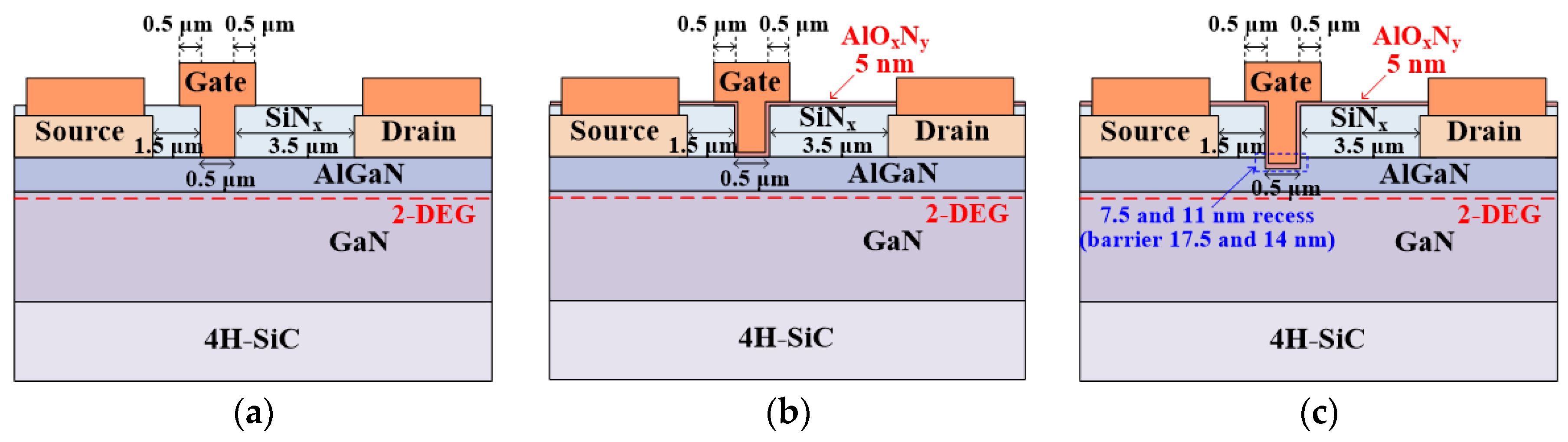
2. Experimental Methods

The AlGaN/GaN-on-SiC wafer was procured from a commercial wafer vendor. The epitaxial layers consisted of a 25 nm unintentionally doped AlxGa1−xN (x = 0.255) barrier layer, a 2 μm GaN buffer layer with a Fe-doped region away from the channel, and a nucleation layer on a 500 μm 4H-SiC semi-insulating substrate. The device fabrication was initiated with solvent cleaning, which was followed by a diluted HF (10:1) treatment for 5 min. for the removal of surface contaminants and native oxides. After the cleaning of the wafer, a 100 nm SiNx film was pre-passivated while using the catalytic chemical vapor deposition (Cat-CVD) method to protect the GaN surface during the high-temperature ohmic annealing [25]. Subsequently, a Si/Ti/Al/Mo/Au (= 5/20/80/35/50 nm) ohmic metal stack was evaporated and annealed at 800 °C for 1 min. in N2 ambient. Mesa isolation was carried out using low-damage Cl2/BCl3-based inductively coupled plasma reactive ion etching (ICP-RIE). The mesa isolation depth was ~550 nm. The pre-passivated SiNx layer was removed using a low damage dry etching process with SF6 plasma in order to remove the damaged interface between the pre-passivation layer and AlGaN surface [26]. A new 140 nm SiNx passivation layer was subsequently re-deposited using Cat-CVD. After the patterning of the gate region, the SiNx passivation layer from the gate foot region was etched away using low-damage SF6 plasma etching. Subsequently, the AlGaN layer under the gate region was recessed while using a low-power Cl2/BCl3-based ICP-RIE. After the completion of the gate recess process, a 5 nm AlOxNy thin film was deposited as a gate insulator using a PEALD system. The detailed optimization of the PEALD AlOxNy film was previously reported in Ref. [22]. According to x-ray photoelectron spectroscopy analysis, the nitrogen incorporation in AlOxNy was ~4%. The gate electrode was formed by the Ni/Mo/Au (= 40/15/400 nm) evaporation. Non-recess MIS-gate and Schottky-gate HEMTs were also fabricated for comparison. The various gate schemes that were compared in this study were Schottky-gate, non-recess MIS, 7.5 nm recess MIS (i.e., with a remaining AlGaN barrier thickness of 17.5 nm), and 11 nm recess MIS (i.e., with a remaining AlGaN barrier thickness of 14 nm) structures. The fabricated devices had a source-to-gate distance of 1.5 μm, a gate foot length of 0.5 μm, and a gate-to-drain distance of 3.5 μm. Figure 1 shows the cross-sectional schematics of the fabricated devices.

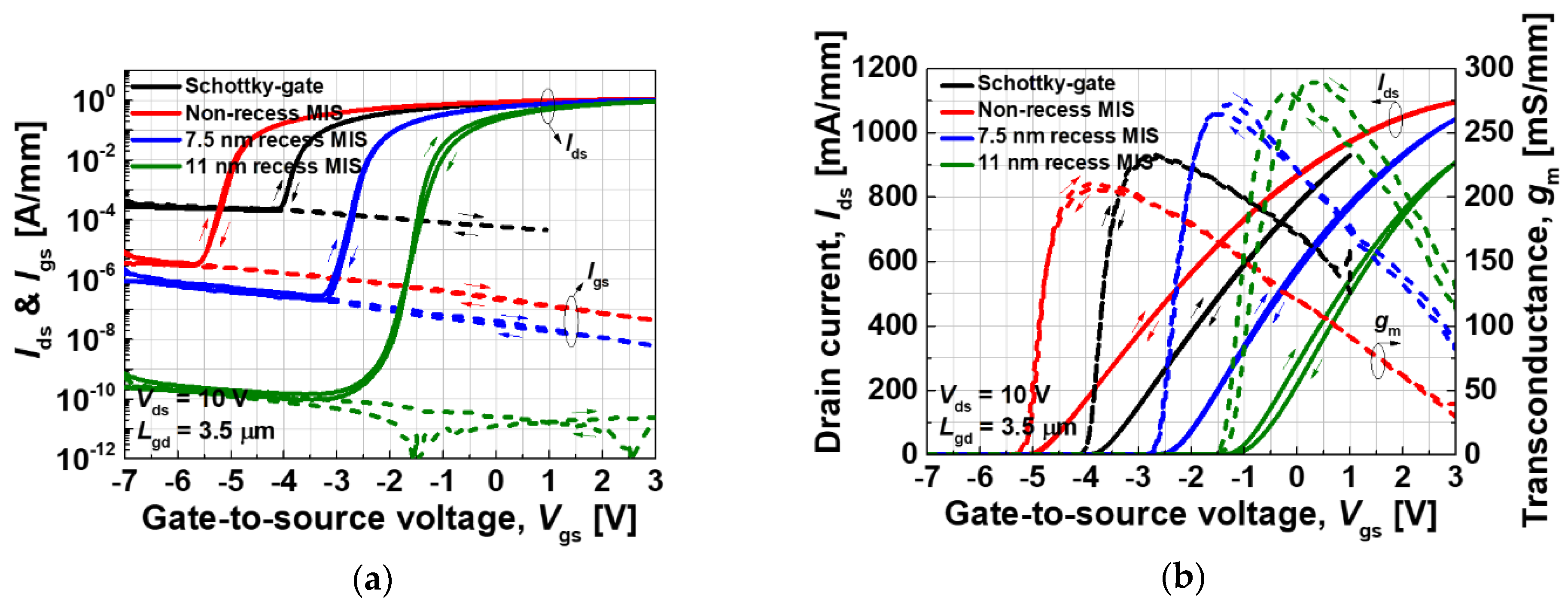
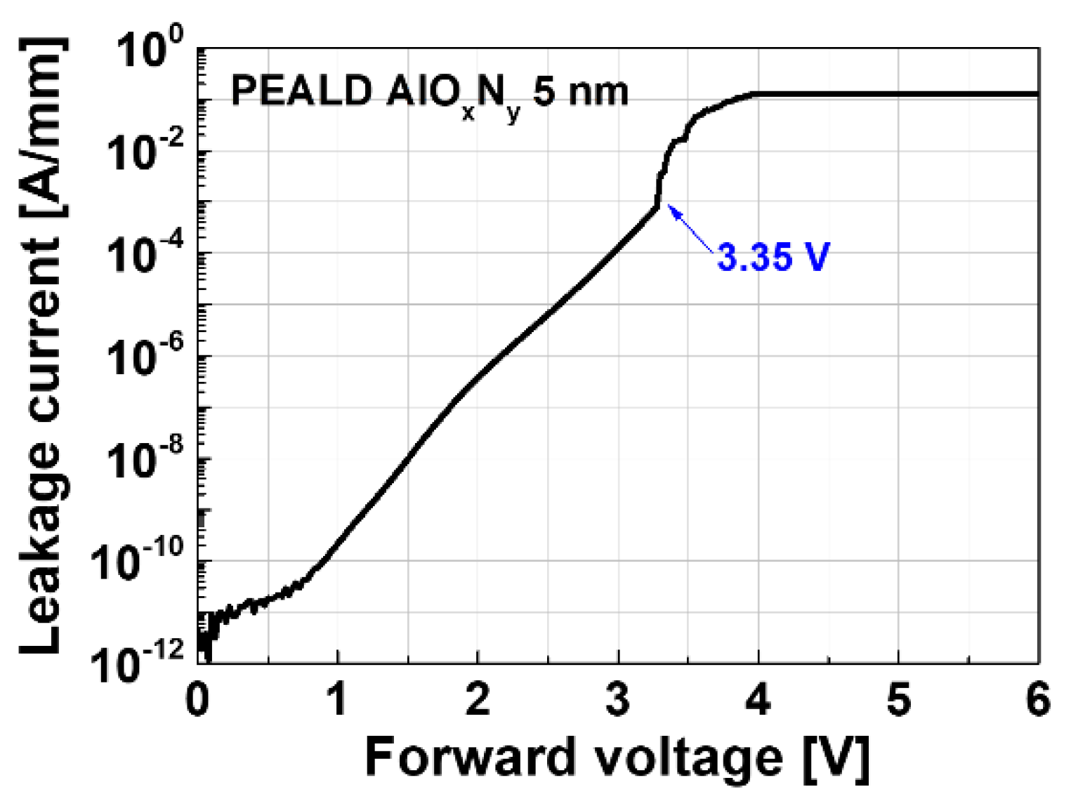
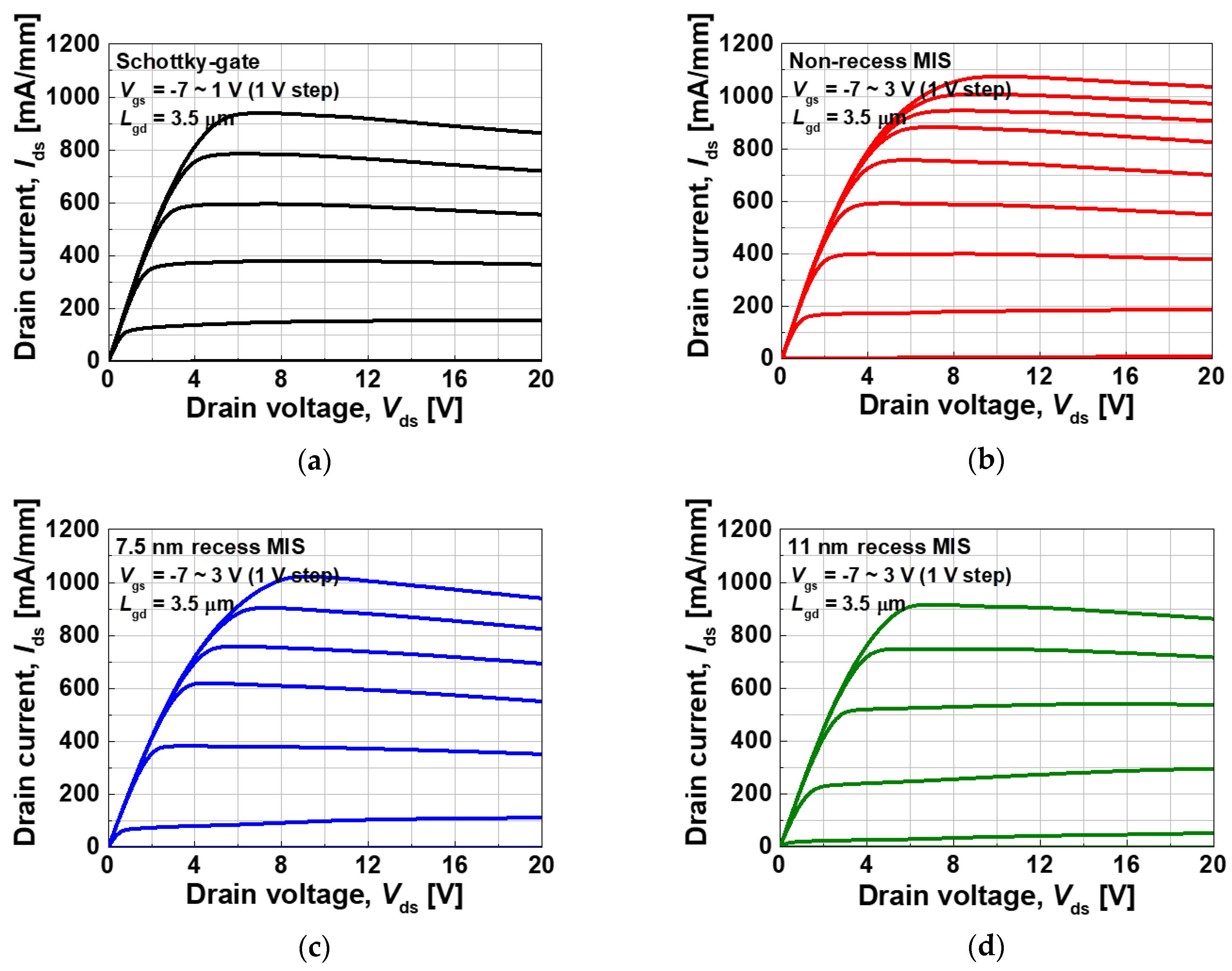
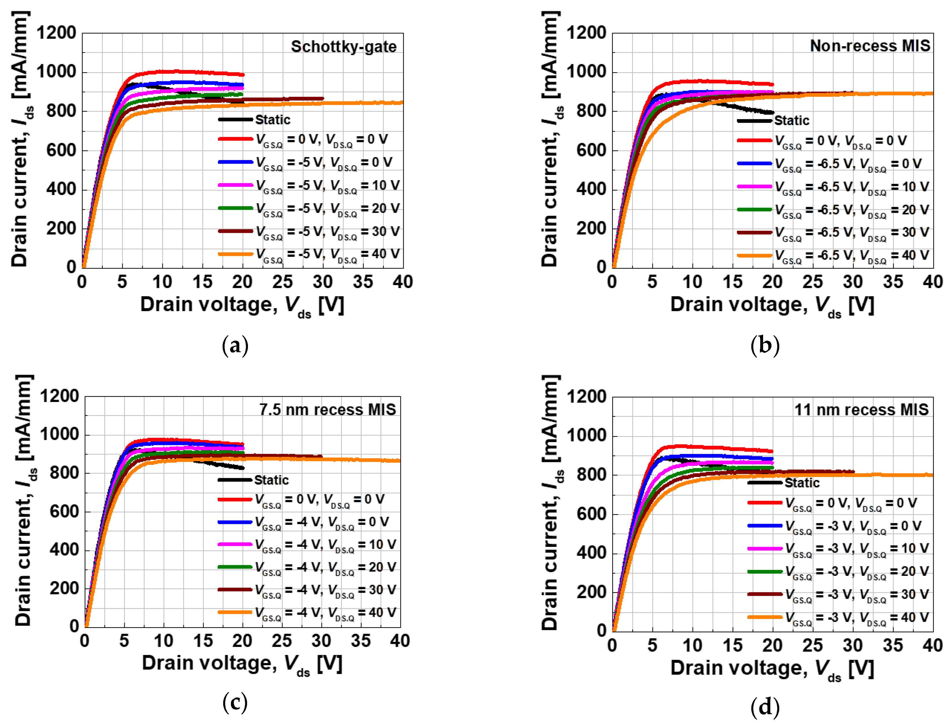
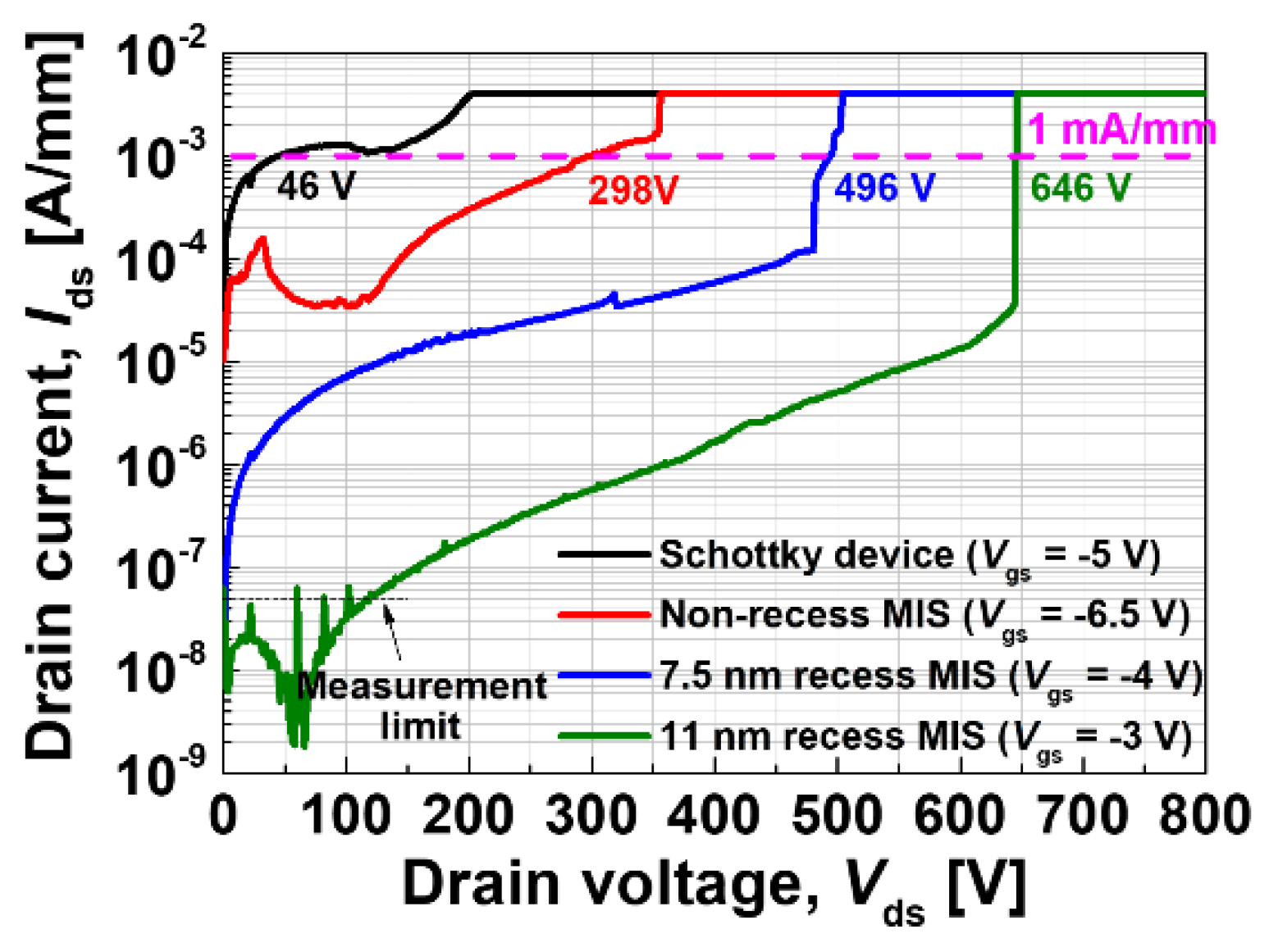
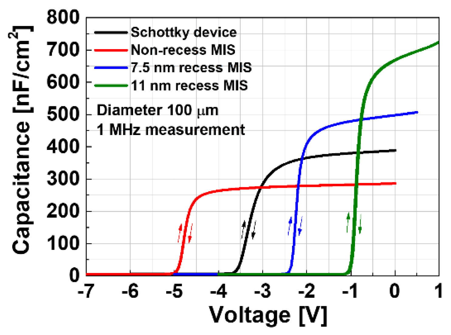
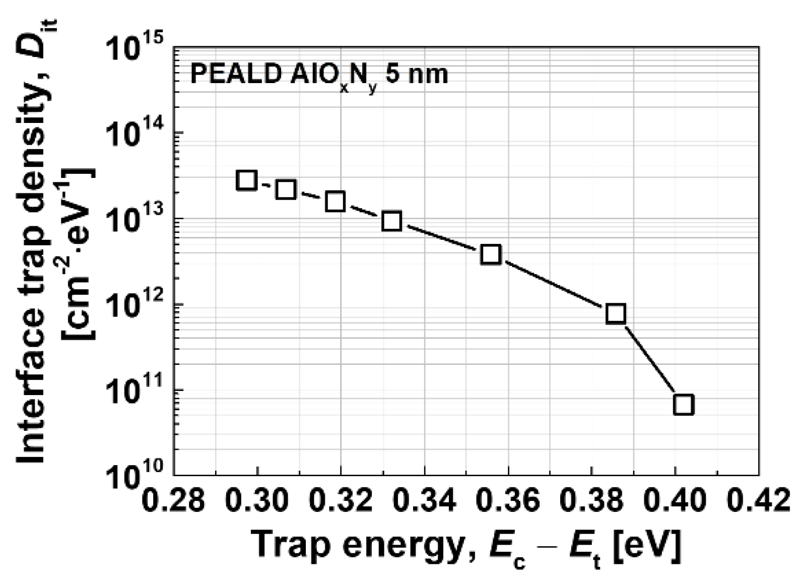
3. Results and Discussion

The transfer current-voltage (I-V) characteristics of the fabricated devices were measured at Vds = 10 V, during which forward and reverse direction sweeps were carried out to investigate the hysteresis characteristics. Negligible hysteresis was observed for all devices, except the 11 nm recess MIS device, as shown in Figure 2. The fabricated Schottky-gate device exhibited a maximum transconductance (gm.max) of 231 mS/mm with the gate leakage and an off-state drain leakage current density of ~2 × 10⁻⁴ A/mm. The non-recess MIS structure exhibited a gm.max of 211 mS/mm with the gate leakage and an off-state drain leakage current density of ~10−6 A/mm. Although the gm.max of the non-recess MIS device was slightly lower than that of the Schottky-gate device due to an increase in the effective barrier thickness [15,16], the gate leakage current was dramatically reduced by two orders of magnitude by employing the MIS gate. In addition, the recessed MIS devices exhibited superior characteristics in both leakage current and gm.max, in comparison with the Schottky and non-recess MIS gate devices. The 7.5 and 11 nm recess MIS devices had leakage current densities of ~3 × 10⁻⁷ A/mm and ~10−10 A/mm, respectively. The improvement in gm.max was caused due to the reduced effective barrier thickness. While the Schottky forward turn-on characteristics limit the maximum positive gate voltage range for the Schottky-gate device, the MIS and the recessed MIS gate configurations allow for a higher positive gate voltage range due to the insulating AlOxNy blocking layer. For example, the forward gate breakdown characteristics that were measured for a 11 nm recess MIS-gate structure exhibited a forward gate breakdown voltage of 3.35 V, which corresponded to a breakdown field of ~6.6 MV/cm (see Figure 3).
Figure 4 illustrates the output characteristics of the fabricated devices. It should be noted that the gate voltage ranges from −7 to 3 V for the MIS gate devices, while it ranges from −7 to 1 V for the Schottky-gate device because of the forward Schottky turn-on problem [4]. The Schottky-gate, non-recess MIS, 7.5 nm recess MIS, and 11 nm recess MIS devices exhibited maximum drain currents of 939, 1075, 1023, and 916 mA/mm, respectively. The higher voltage range of the MIS devices resulted in a higher maximum drain current density. All of the devices exhibited excellent drain current saturation and pinch-off characteristics.
The pulsed I-V characteristics for the different devices were measured by employing different quiescent drain bias voltages in order to investigate the current collapse characteristics, as shown in Figure 5. The quiescent gate bias voltages were determined by taking account of deep pinch-off conditions. The pulse width was 200 ns with a period of 1 ms. All of the devices, which were associated with a high-quality passivation process, exhibited excellent pulsed I-V characteristics without an additional field plate. The non-recess MIS and the 7.5 nm recess MIS devices exhibited slightly better characteristics in comparison with the Schottky-gate device, which elucidates that the additional AlOxNy film was effective in further suppressing the surface trapping effects. It was assumed that a relatively worse pulsed characteristic of the 11 nm recess MIS device was found due to the presence of a very thin reminiscent AlGaN barrier, thus causing a more sensitive response to any surface trapping effects.
Figure 6 compares the off-state breakdown characteristics of the fabricated devices measured under the deep pinch-off conditions. For the conventional Schottky-gate device, the breakdown voltage defined at 1 mA/mm was found to be 46 V with high off-state leakage current. In contrast, the non-recess MIS device exhibited a breakdown voltage of 298 V with the suppressed leakage current in comparison with the Schottky-gate device. The recessed MIS gate devices achieved further enhancements in breakdown voltage and a significant reduction in leakage current. It is speculated that the leakage current that was observed in this work was mainly induced near the AlGaN surface or passivation interface, because the leakage current level decreased with increasing the recess depth. The 7.5 nm recess MIS and 11 nm recess MIS devices exhibited breakdown voltages of 496 and 646 V, respectively. It was evident that the improved breakdown characteristics of the recessed MIS devices were associated with the decrease in the leakage current along with the reduced electric field due to the voltage drop across the gate insulator.
Capacitance-voltage (C-V) measurements were carried out for Schottky-gate and MIS-gate devices in order to investigate the effective gate capacitance and the interface quality of the MIS devices. Figure 7 compares the measured C-V characteristics, where negligible hysteresis was observed, regardless of the device type, which means that the interface conditions of the MIS and recessed MIS devices are as good as the Schottky-gate devices. The effective capacitance can be expressed by employing a series connection of the AlGaN barrier and AlOxNy insulator, from which the extracted dielectric constant of the AlOxNy film was 8.4. The interface trap density was extracted by a conductance method [27], where the C-V measurements were carried out from 1 kHz to 1 MHz, in order to further evaluate the MIS interface conditions. The extracted interface trap density was < 1011 cm−2·eV−1 at the trap energy level of 0.4 eV from the conduction band edge, which indicates excellent MIS interface quality, as shown in Figure 8.
The small-signal characteristics were measured for the fabricated devices with a channel width of 2 × 50 μm. The S-parameter for each device was measured from 100 MHz to 40 GHz at the drain voltage of 28 V, and the gate bias point was set at the maximum gm point. The measured cut-off frequency (fT) and the maximum oscillation frequency (fMAX) were extracted from the current gain (|H21|) and the maximum stable/available gain (MSG/MAG), respectively, as shown in Figure 9. The Schottky-gate device exhibited fT of 18.9 GHz and an fMAX of 60 GHz, whereas the non-recess MIS device exhibited fT of 18.7 GHz and fMAX of 54 GHz. The highest fT of 21.7 GHz was achieved by the 7.5 nm recess MIS structure. On the other hand, the 11 nm recess MIS device exhibited the lowest fT of 13.7 GHz. The gate capacitance was measured for different devices in order to analyze the behavior of fT as a function of the gate structure. The gate capacitance varied widely for different gate structures, as shown in Figure 7. The degradation in fT for the 11 nm recess MIS device can be explained by the high gate capacitance value that is caused by the very thin effective barrier thickness. This is a trade-off relationship for fT between gm and the gate capacitance [28]. The degradation of fMAX for recessed MIS devices is associated with increased feedback capacitance [28]. An additional source field plate process can be used to reduce the feedback capacitance and mitigate the degradation of fMAX.
Figure 10 shows the comparison of J-FOM (= fT × BVgd) as a function of the gate length for various GaN-based HEMTs [20,21,29,30,31,32,33,34,35,36,37,38,39,40,41,42,43]. The MIS-HEMTs that were fabricated in this study exhibited the J-FOM in the range between 5.57 and 10.67 THz·V, which are the state-of-the-art values reported for GaN-based HEMTs. It is suggested that the thin AlOxNy layer is an excellent gate insulator for reducing the gate leakage current and enhancing the breakdown voltage of AlGaN/GaN HEMT.

4. Conclusions

A 5 nm AlOxNy thin film was investigated for its use as a gate insulator for AlGaN/GaN-on-SiC HEMT. A high-quality PEALD AlOxNy deposition process was utilized for device fabrication where the gate structure was varied to be Schottky-gate, MIS-gate, and recessed MIS-gates. The gate leakage current and the breakdown voltage were significantly improved by employing a thin AlOxNy MIS-gate configuration, which led to a significant improvement in the J-FOM values. The AlOxNy MIS-HEMTs attained state-of-the-art J-FOM values in the range of 5.57 to 10.76 THz·V. Moreover, by employing the pulsed and C-V characteristics, it was confirmed that the AlOxNy MIS had excellent interface conditions. The maximum fT was achieved while using a shallow recess depth due to the trade-off relationship between gm and gate capacitance; thus, the gate recess depth must be carefully optimized.

Author Contributions

Conceptualization, H.-S.K. and H.-Y.C.; methodology, H.-S.K. and M.-J.K.; validation, H.-S.K. and M.-J.K.; formal analysis, H.-S.K.; investigation, H.-S.K., M.-J.K., J.J.K., and K.-S.S.; data curation, H.-S.K. and M.-J.K.; writing—original draft preparation, H.-S.K.; writing—review and editing, H.-Y.C.; visualization, H.-S.K.; supervision, J.J.K., K.-S.S., and H.-Y.C.; funding acquisition, H.-Y.C. All authors have read and agreed to the published version of the manuscript.

Funding

This work was supported by Civil-Military Technology Cooperation Program (No. 17-CM-MA-03), and Basic Science Research Programs (2015R1A6A1A03031833 and 2019R1A2C1008894), and Global Ph.D. Fellowship Program (NRF-2018H1A2A1060832) through NRF Grant funded by the Korea Government.

Conflicts of Interest

The authors declare no conflict of interest.

References

  1. Mishra, U.K.; Parikh, P.; Wu, Y.-F. AlGaN/GaN HEMTs-An Overview of Device Operation and Applications. Proc. IEEE 2002, 90, 1022–1031. [Google Scholar] [CrossRef] [Green Version]
  2. Higashiwaki, M.; Mimura, T.; Matsui, T. AlGaN/GaN Heterostructure Field-Effect Transistors on 4H-SiC Substrates with Current-Gain Cutoff Frequency of 190 GHz. Appl. Phys. Express 2008, 1, 021103. [Google Scholar] [CrossRef]
  3. Lee, M.-S.; Kim, D.; Eom, S.; Cha, H.-Y.; Seo, K.-S. A Compact 30-W AlGaN/GaN HEMTs on Silicon Substrate with Output Power Density of 8.1 W/mm at 8 GHz. IEEE Electron Device Lett. 2014, 35, 995–997. [Google Scholar] [CrossRef]
  4. Mizuno, S.; Ohno, Y.; Kishimoto, S.; Maezawa, K.; Mizutani, T. Large Gate Leakage Current in AlGaN/GaN High Electron Mobility Transistors. Jpn. J. Appl. Phys. 2002, 41, 5125–5126. [Google Scholar] [CrossRef]
  5. Kanamura, M.; Kikkawa, T.; Iwai, T.; Imanishi, K.; Kubo, T.; Joshin, K. An Over 100 W n-GaN/n-AlGaN/GaN MIS-HEMT Power Amplifier for Wireless Base Station Applications. In Proceedings of the IEEE International Electron Devices Meeting (IEDM), Washington, DC, USA, 5–7 December 2005. [Google Scholar] [CrossRef]
  6. Adivarahan, V.; Gaevshi, M.; Sun, W.H.; Fatima, H.; Koudymov, A.; Saygi, S.; Simin, G.; Yang, J.; Khan, M.A.; Tarakji, A.; et al. Submicron Gate Si3N4/AlGaN/GaN-Metal-Insulator-Semiconductor Heterostructure Field-Effect Transistors. IEEE Electron Device Lett. 2003, 24, 541–543. [Google Scholar] [CrossRef]
  7. Kikuta, D.; Ao, J.P.; Ohno, Y. Gate leakage and electrical performance of AlGaN/GaN MIS-type HFET with evaporated silicon oxide layer. Solid-State Electron. 2006, 50, 316–321. [Google Scholar] [CrossRef]
  8. Yagi, S.; Shimizu, M.; Inada, M.; Yamamoto, Y.; Piao, G.; Okumura, H.; Yano, Y.; Akutsu, N.; Ohashi, H. High breakdown voltage AlGaN/GaN MIS-HEMT with SiN and TiO2 gate insulator. Solid-State Electron. 2006, 50, 1057–1061. [Google Scholar] [CrossRef]
  9. LaRoche, J.; Hoke, W.; Altman, D.; McClymonds, J.; Alcorn, P.; Smith, K.; Chumbes, E.; Letaw, J.; Kazior, T. Performance and Reliability of GaN MISHEMTs and MMIC Fabricated from GaN Grown on High Resistance <111> Si Substrates by Molecular Beam Epitaxy. In Proceedings of the International Conference on Compound Semiconductor Manufacturing Technology (CS MANTECH), New Orleans, LA, USA, 13–16 May 2013; pp. 345–348. [Google Scholar]
  10. Khan, M.A.; Hu, X.; Tarakji, A.; Simin, G.; Yang, J.; Gaska, R.; Shur, M.S. AlGaN/GaN metal-oxide-semiconductor heterostructure field-effect transistors on SiC substrates. Appl. Phys. Lett. 2000, 77, 1339–1341. [Google Scholar] [CrossRef] [Green Version]
  11. Hu, X.; Koudymov, A.; Simin, G.; Yang, J.; Khan, M.A.; Tarakji, A.; Shur, M.S.; Gaska, R. Si3N4/AlGaN/GaN-metal-insulator-semiconductor heterostructure field-effect transistors. Appl. Phys. Lett. 2001, 79, 2832–2834. [Google Scholar] [CrossRef] [Green Version]
  12. Hashizume, T.; Ootomo, S.; Hasegawa, H. Al2O3-based surface passivation and insulated gate structure for AlGaN/GaN HFETs. Phys. Status Solidi (C) 2001, 0, 2380–2384. [Google Scholar] [CrossRef]
  13. Kawano, A.; Kishimoto, S.; Ohno, Y.; Maezawa, K.; Mizutani, T.; Ueno, H.; Ueda, T.; Tanaka, T. AlGaN/GaN MIS-HEMTs with HfO2 gate insulator. Phys. Status Solidi (C) 2007, 7, 2700–2703. [Google Scholar] [CrossRef]
  14. Mehandru, R.; Luo, B.; Kim, J.; Ren, F.; Gila, B.P.; Onstine, A.H.; Abernathy, C.R.; Pearton, S.J.; Gotthold, D.; Birkhahn, R.; et al. AlGaN/GaN metal-oxide-semiconductor high electron mobility transistors using Sc2O3 as the gate oxide and surface passivation. Appl. Phys. Lett. 2003, 82, 2530–2532. [Google Scholar] [CrossRef]
  15. Khan, M.A.; Hu, X.; Sumin, S.; Lunev, A.; Yang, J.; Shur, M.S. AlGaN/GaN Metal Oxide Semiconductor Heterostructure Field Effect Transistor. IEEE Electron Device Lett. 2000, 21, 63–65. [Google Scholar] [CrossRef]
  16. Park, K.-Y.; Cho, H.-I.; Choi, H.-C.; Bae, Y.-H.; Lee, C.-S.; Lee, J.-L.; Lee, J.-H. Device Characteristics of AlGaN/GaN MIS-HFET Using Al2O3-HfO2 Laminated High-k Dielectric. Jpn. J. Appl. Phys. 2004, 43, L1433–L1435. [Google Scholar] [CrossRef]
  17. Marso, M.; Heidelberger, G.; Indlekofer, K.M.; Bernát, J.; Fox, A.; Korodoš, P.; Lüth, H. Origin of Improved RF Performance of AlGaN/GaN MOSHFETs Compared to HFETs. IEEE Trans. Electron Devices 2006, 53, 1517–1523. [Google Scholar] [CrossRef]
  18. Maroldt, S.; Haupt, C.; Pletschen, W.; Müller, S.; Quay, R.; Ambacher, O.; Schippel, C.; Schwierz, F. Gate-Recessed AlGaN/GaN Based Enhancement-Mode Electron Mobility Transistors for High Frequency Operation. Jpn. J. Appl. Phys. 2009, 48, 04C083. [Google Scholar] [CrossRef]
  19. Kim, D.-H.; Park, H.; Eom, S.-K.; Jeong, J.-S.; Cha, H.-Y.; Seo, K.-S. Ka-Band MMIC Using AlGaN/GaN-on-Si With Recessed High-k Dual MIS Structure. IEEE Electron Device Lett. 2018, 39, 995–998. [Google Scholar] [CrossRef]
  20. Downey, B.P.; Meyer, D.J.; Katzer, D.S.; Roussos, J.A.; Pan, M.; Gao, X. SiNx/InAlN/AlN/GaN MIS-HEMTs With 10.8 THz·V Johnson Figure of Merit. IEEE Electron Device Lett. 2014, 35, 527–529. [Google Scholar] [CrossRef]
  21. Fletcher, A.S.A.; Nirmal, D.; Arivazhagan, L.; Ajayan, J.; Varghese, A. Enhancement of Johnson figure of merit in III-V HEMT combined with discrete field plate and AlGaN blocking layer. Int. J. RF Microw. Comput. Aided Eng. 2020, 30, 22040. [Google Scholar] [CrossRef]
  22. Kang, M.-J.; Eom, S.-K.; Kim, H.-S.; Lee, C.-H.; Cha, H.-Y.; Seo, K.-S. Normally-off recessed-gate AlGaN/GaN MOS-HFETs with plasma enhanced atomic layer deposited AlOxNy gate insulator. Semicond. Sci. Technol. 2019, 34, 055018. [Google Scholar] [CrossRef]
  23. Nakazawa, S.; Shin, H.-A.; Tsurumi, N.; Anda, Y.; Hatsuda, T.; Ueda, T.; Nozaki, M.; Yamada, T.; Hosoi, T.; Shimura, T.; et al. Fast Switching Performance by 20 A/730 V AlGaN/GaN MIS-HEMT Using AlON Gate Insulator. In Proceedings of the IEEE International Electron Devices Meeting (IEDM), San Francisco, CA, USA, 2–6 December 2017. [Google Scholar] [CrossRef]
  24. Hosoi, T.; Watanabe, K.; Nozaki, M.; Yamada, T.; Shimura, T.; Watanabe, H. Mobility enhancement in recessed-gate AlGaN/GaN MOS-HFETs using an AlON gate insulator. Jpn. J. Appl. Phys. 2019, 58, SCCD16. [Google Scholar] [CrossRef]
  25. Her, J.-C.; Cho, H.-J.; Yoo, C.-S.; Cha, H.-Y.; Oh, J.-E.; Seo, K.-S. SiNx Prepassivation of AlGaN/GaN High-Electron-Mobility Transistors Using Remote-Mode Plasma-Enhanced Chemical Vapor Deposition. Jpn. J. Appl. Phys. 2010, 49, 041002. [Google Scholar] [CrossRef]
  26. Lee, N.-H.; Lee, M.; Choi, W.; Kim, D.; Jeon, N.; Choi, S.; Seo, K.-S. Effects of various surface treatments on gate leakage, subthreshold slope, and current collapse in AlGaN/GaN high-electron-mobility transistors. Jpn. J. Appl. Phys. 2014, 53, 4. [Google Scholar] [CrossRef] [Green Version]
  27. Schroder, D.K. Semiconductor Material and Device Characterization, 3rd ed.; John Wiley & Sons: Hoboken, NJ, USA, 2006; pp. 347–350. [Google Scholar]
  28. Dehan, M. Characterization and Modeling of SOI RF Integrated Components; Presses Universitaires de Louvain: Louvain-la-Neuve, Belgium, 2003; pp. 103–107. [Google Scholar]
  29. Dumka, D.C.; Lee, C.; Tserng, H.Q.; Saunier, P. RF reliability performance of AlGaN/GaN HEMTs onSi substate at 10 GHz. Elect. Lett. 2004, 40, 1554–1556. [Google Scholar] [CrossRef]
  30. Johnson, J.W.; Piner, E.L.; Vescan, A.; Therrien, R.; Rajagopal, P.; Roberts, J.C.; Brown, J.D.; Singhal, S.; Linthicum, K.J. 12 W/mm AlGaN-GaN HFETs on Silicon Substrates. IEEE Electron Device Lett. 2004, 25, 459–461. [Google Scholar] [CrossRef]
  31. Yoshida, S.; Tanomura, M.; Murase, Y.; Yamanoguchi, K.; Ota, K.; Matsunaga, K.; Shimawaki, H. A 76 GHz GaN-on-Silicon Power Amplifier for Automotive Radar System. In Proceedings of the 2009 IEEE MTT-S International Microwave Symposium Digest, Boston, MA, USA, 7–12 June 2009; pp. 665–668. [Google Scholar] [CrossRef]
  32. Hoshi, S.; Itoh, M.; Marui, T.; Okita, H.; Morino, Y.; Tamai, I.; Toda, F.; Seki, S.; Egawa, T. 12.88 W/mm GaN High Electron Mobility Transistor on Silicon Substrate for High Voltage Operation. Appl. Phys. Express 2009, 2, 061001. [Google Scholar] [CrossRef]
  33. Sun, H.; Alt, A.R.; Benedickter, H.; Bolognesi, C.R.; Feltin, E.; Carlin, J.-F.; Gonschorek, M.; Grandjean, N. Ultrahigh-Speed AlInN/GaN High Electron Mobility Transistors Grown on (111) High-Resistivity Silicon with FT = 143 GHz. Appl. Phys. Express 2010, 2, 094101. [Google Scholar] [CrossRef]
  34. Shinohara, K.; Regan, D.C.; Tang, Y.; Corrion, A.L.; Brown, D.F.; Wong, J.C.; Robinson, J.F.; Fung, H.H.; Schmitz, A.; Oh, T.C.; et al. Scaling of GaN HEMTs and Schottky Didoes for Submillimeter-Wave MMIC Applications. IEEE Trans. Electron Devices 2013, 60, 2982–2996. [Google Scholar] [CrossRef]
  35. Schuette, M.L.; Ketterson, A.; Song, B.; Beam, D.; Chou, T.-M.; Pilla, M.; Tserng, H.-Q.; Gao, X.; Guo, S.; Fay, P.J.; et al. Gate-Recessed Integrated E/D GaN HEMT Technology With fT/fmax > 300 GHz. IEEE Electron Device Lett. 2013, 34, 741–743. [Google Scholar] [CrossRef]
  36. Medjdoub, F.; Grimbert, B.; Ducatteau, D.; Rolland, N. Record Combination of Power-Gain Cut-Off Frequency and Three-Terminal Breakdown Voltage for GaN-on-Silicon Devices. Appl. Phys. Express 2013, 6, 044001. [Google Scholar] [CrossRef]
  37. Arulkumaran, S.; Ng, G.I.; Vicknesh, S.; Wang, H.; Ang, K.S.; Kumar, C.M.; Teo, K.L.; Ranjan, K. Demonstration of Submicron-Gate AlGaN/GaN High-Electron-Mobility Transistors on Silicon with Complementary Metal-Oxide-Semiconductor-Compatible Non-Gold Metal Stack. Appl. Phys. Express 2013, 6, 016501. [Google Scholar] [CrossRef]
  38. Arulkumaran, S.; Ng, G.I.; Vicknesh, S. Enhanced Breakdown Voltage with High Johnson’s Figure-of-Merit in 0.3-μm T-gate AlGaN/GaN HEMTs on Silicon by (NH4)2Sx Treatment. IEEE Electron Device Lett. 2013, 34, 1364–1366. [Google Scholar] [CrossRef]
  39. Ranjan, K.; Arulkumaran, S.; Ng, G.I.; Vicknesh, S. High Johnson’s figure of merit (8.32 THz·V) in 0.15-μm conventional T-gate AlGaN/GaN HEMTs on silicon. Appl. Phys. Express 2014, 7, 044102. [Google Scholar] [CrossRef]
  40. Huang, S.; Wei, K.; Liu, G.; Zheng, Y.; Wang, X.; Pang, L.; Kong, X.; Liu, X.; Tang, Z.; Yang, S.; et al. High-fMAX High Johnson’s Figure-of-Merit 0.2-μm Gate AlGaN/GaN HEMTs on Silicon Substrate With AlN/SiNx Passivation. IEEE Electron Device Lett. 2014, 35, 315–317. [Google Scholar] [CrossRef]
  41. Tsou, C.-W.; Lin, C.-Y.; Lian, Y.-W.; Hsu, S.S.H. 101-GHz InAlN/GaN HEMTs on Silicon with High Johnson’s Figure-of-Merit. IEEE Trans. Electron Devices 2015, 62, 2675–2678. [Google Scholar] [CrossRef]
  42. Yang, L.; Mi, M.; Hou, B.; Zhang, H.; Zhu, J.; Zhu, Q.; Lu, Y.; Zhang, M.; He, Y.; Chen, L.; et al. Enhanced gm and fT With High Johnson’s Figure-of-Merit in Thin Barrier AlGaN/GaN Figure-of-Merit in Thin Barrier AlGaN/GaN HEMTs by TiN-Based Source Contact Ledge. IEEE Electron Device Lett. 2017, 38, 1563–1566. [Google Scholar] [CrossRef]
  43. Fletcher, A.S.A.; Nirmal, D.; Ajayan, J.; Arivazhagan, L. Analysis of AlGaN/GaN HEMT using discrete field plate technique for high power and high frequency applications. Int. J. Electron. Commun. 2019, 99, 325–330. [Google Scholar] [CrossRef]
Figure 1. Cross-sectional schematics of the AlGaN/GaN high-electron-mobility transistors (HEMTs): (a) Schottky-gate, (b) non-recess metal-insulator-semiconductor (MIS), and (c) recess MIS structures.
Materials 13 01538 g001
Figure 2. Comparison of the transfer characteristics; (a) drain and gate current characteristics in a logarithmic scale and (b) transconductance characteristics.
Materials 13 01538 g002
Figure 3. Forward breakdown characteristics of a 5 nm AlOxNy film on an 11 nm recessed AlGaN/GaN surface.
Materials 13 01538 g003
Figure 4. Output characteristics of the fabricated devices; (a) Schottky-gate, (b) non-recess MIS, (c) 7.5 nm recess MIS, and (d) 11 nm recess MIS structures.
Materials 13 01538 g004
Figure 5. Pulsed I-V characteristics of the fabricated devices; (a) Schottky-gate, (b) non-recess MIS gate, (c) 7.5 nm recess MIS gate, and (d) 11 nm recess MIS gate.
Materials 13 01538 g005
Figure 6. Off-state breakdown characteristics of the fabricated devices.
Materials 13 01538 g006
Figure 7. Gate capacitance-voltage characteristics of different gate structures in circular process control monitor patterns.
Materials 13 01538 g007
Figure 8. Interface trap density characteristics extracted by a conductance method.
Materials 13 01538 g008
Figure 9. Small-signal characteristics of the fabricated devices; (a) Schottky-gate, (b) non-recess MIS, (c) 7.5 nm recess MIS, and (d) 11 nm recess MIS devices.
Materials 13 01538 g009
Figure 10. J-FOM as a function of gate length reported for GaN-based HEMTs.
Materials 13 01538 g010

