Geometry Control of Source/Drain Electrodes in Organic Field-Effect Transistors by Electrohydrodynamic Inkjet Printing
Abstract
1. Introduction
2. Materials and Methods
2.1. Silver Nanopaste Ink
2.2. Sample Preparation
2.3. Contact Angle Measurements
2.4. Inkjet Printing
2.5. Geometrical Characterization of the Overprints
2.6. Resistivity Measurements of the Overprints
2.7. Organic Field-Effect Transistors
3. Results
3.1. Role of Surface Energy
3.2. Influence of Printing Parameters on Geometry and Resistivity of the Overprints
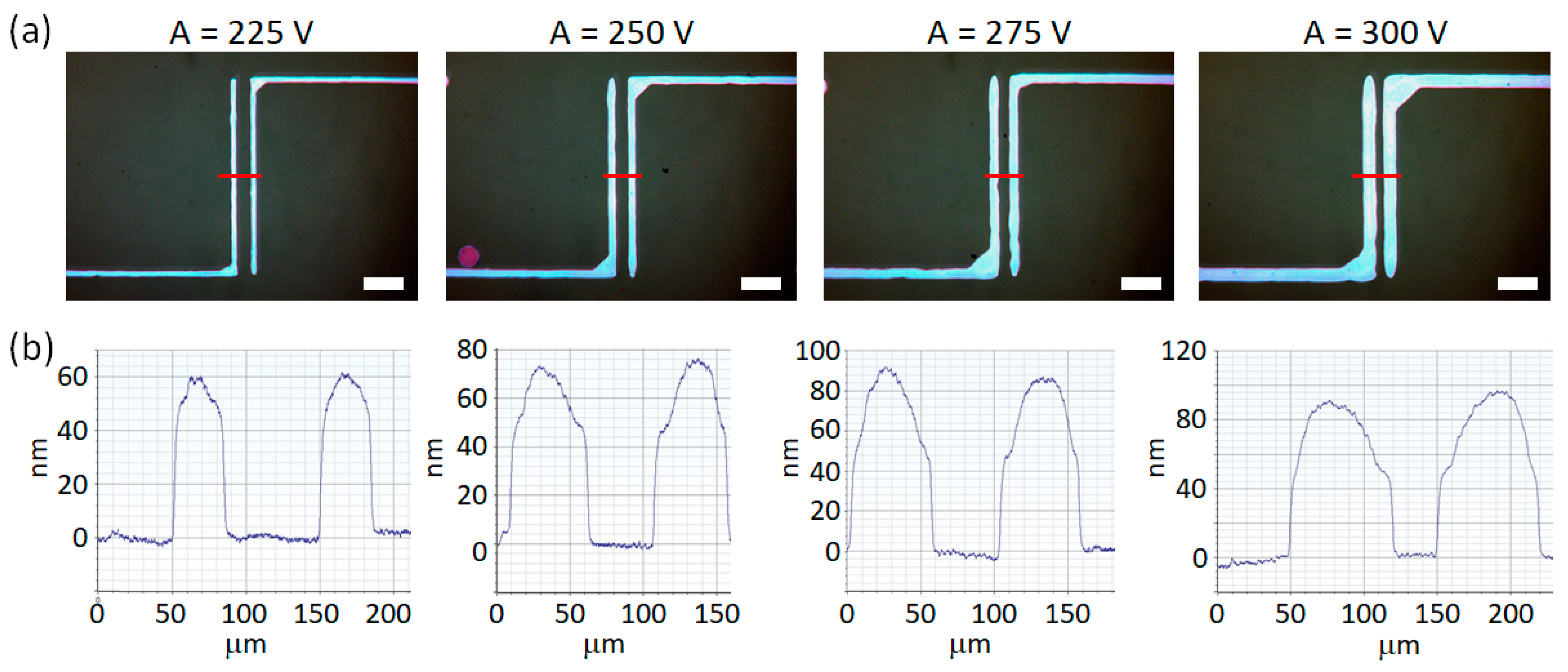
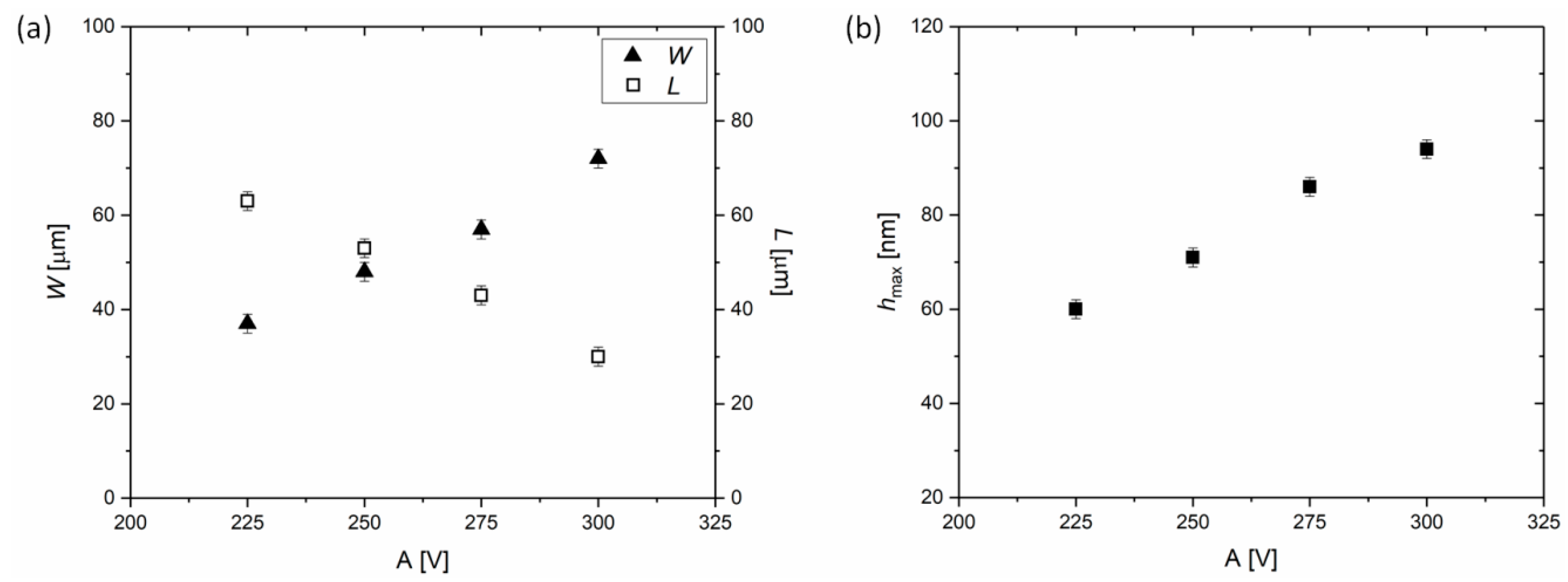
3.2.1. Amplitude of the Voltage Applied
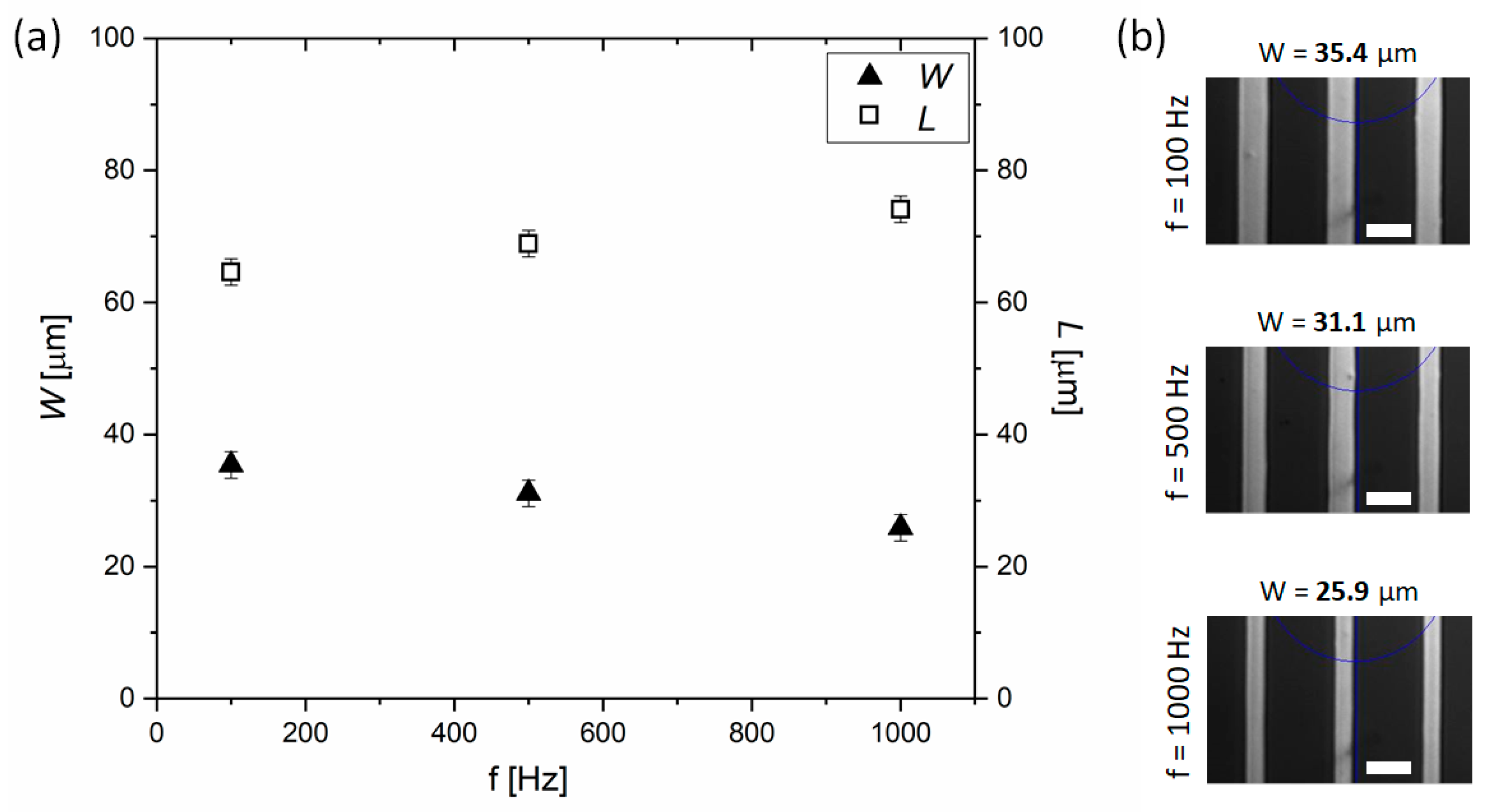
3.2.2. Frequency of the Voltage Waveform
3.2.3. Summary of the Geometrical Features of the Overprints
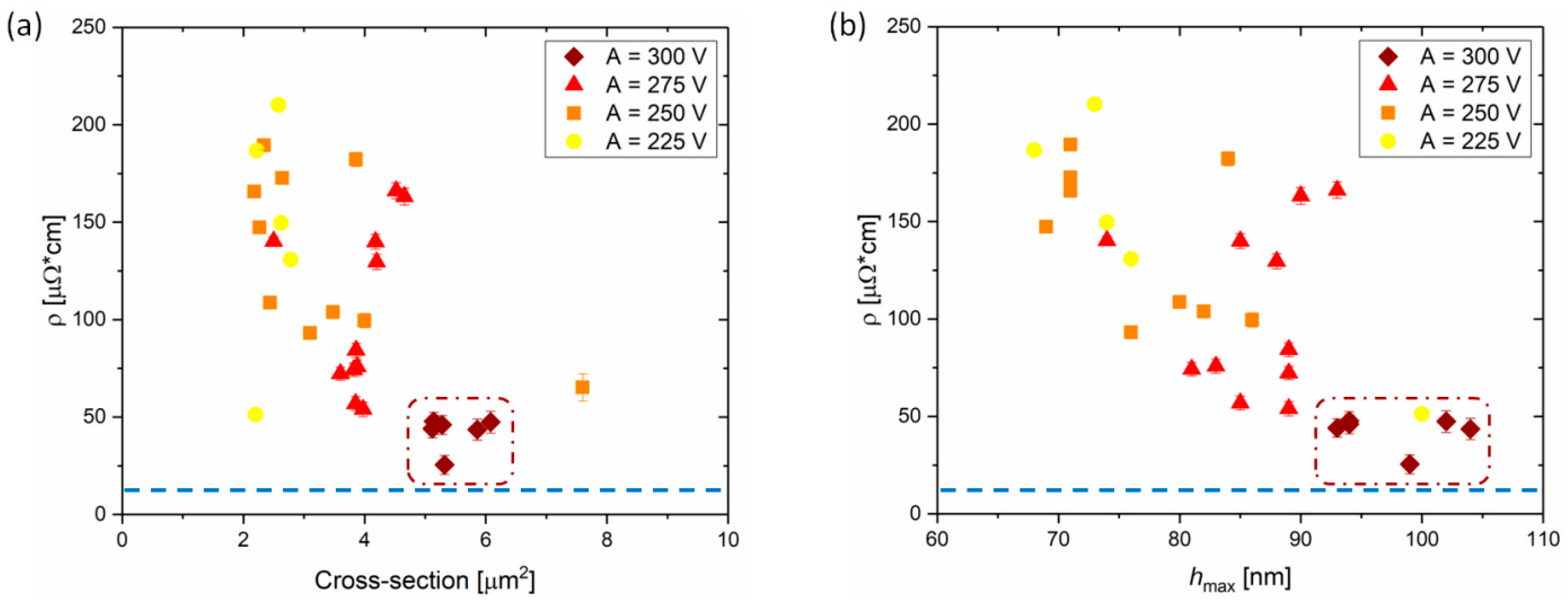
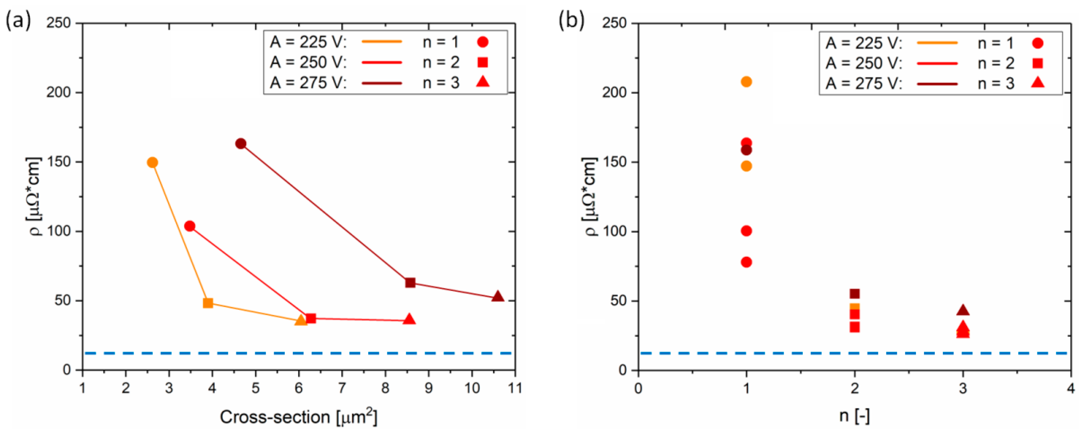
3.2.4. Resistivity of the Overprints
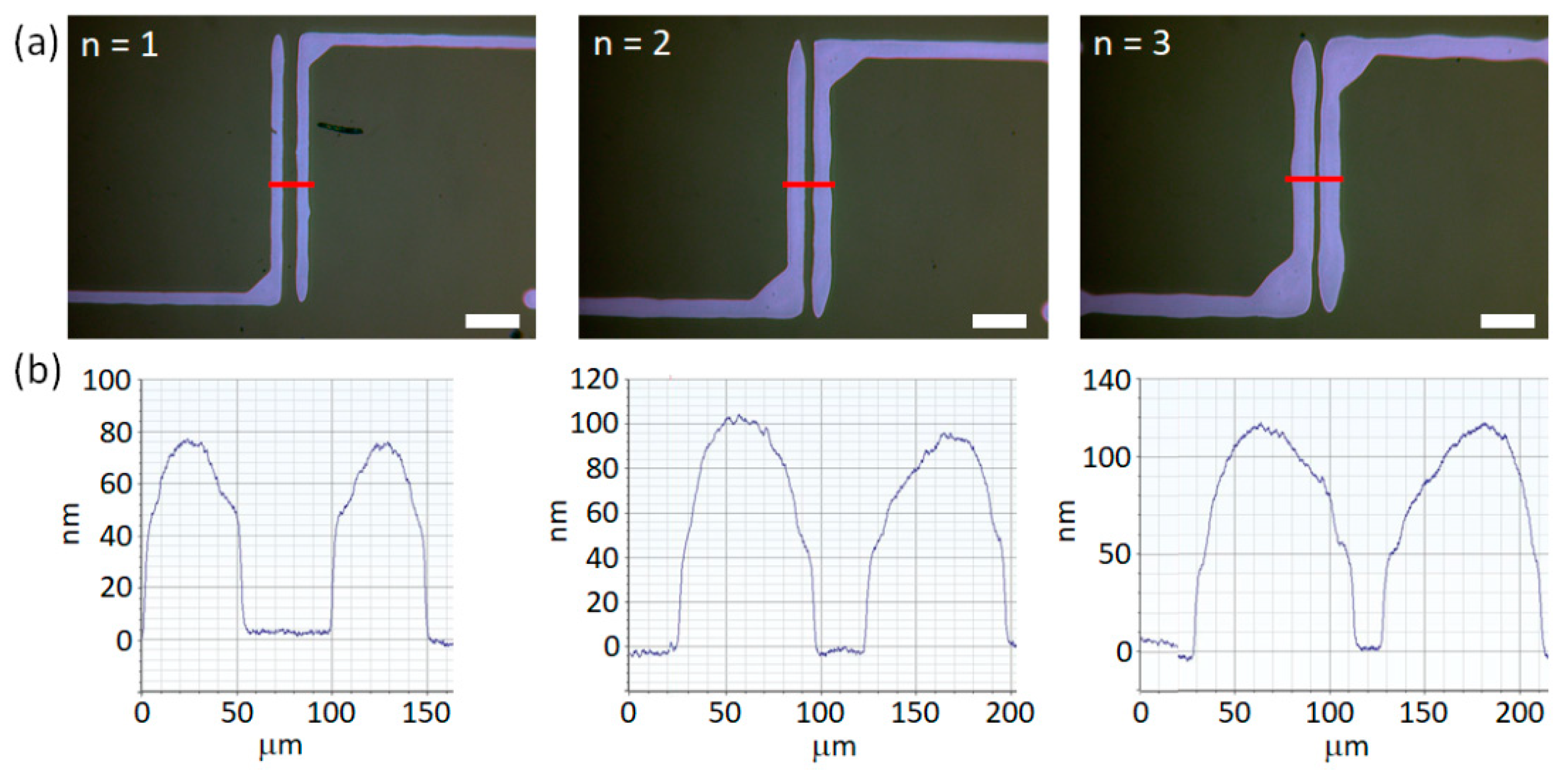
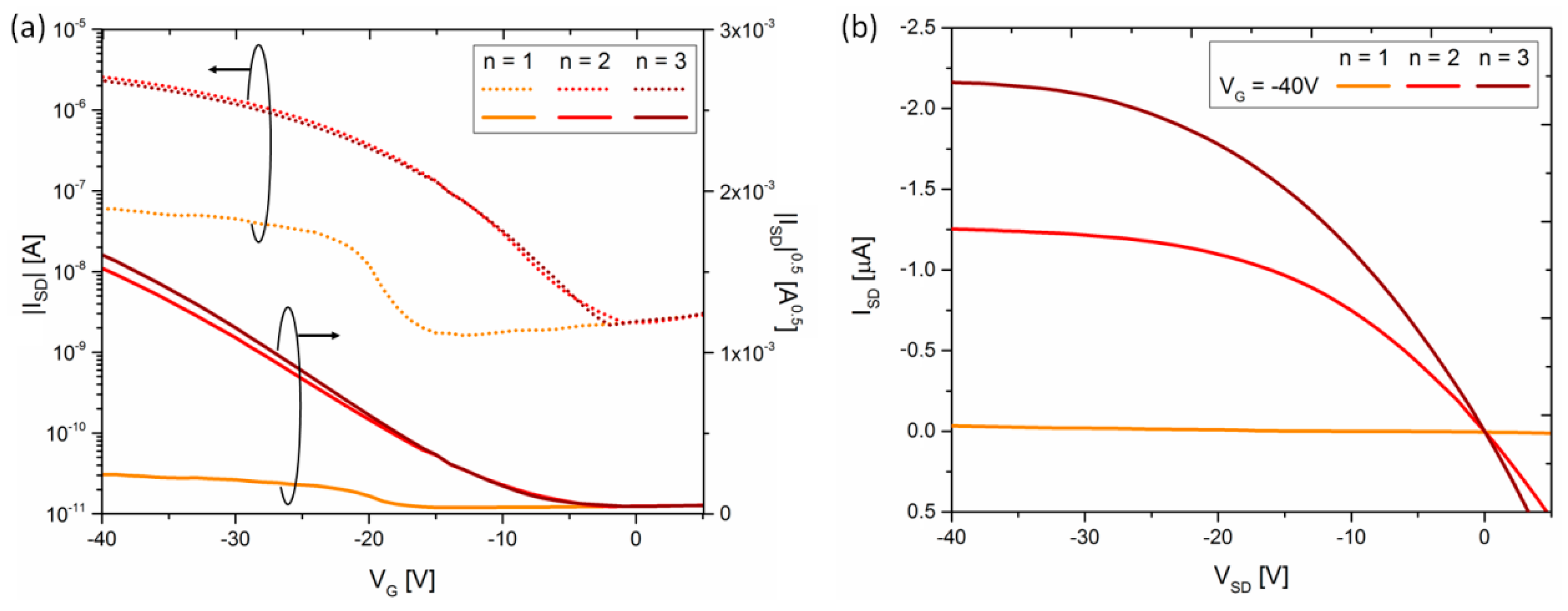
3.3. Optimization of the Number of Overprints
4. Conclusions
Supplementary Materials
Author Contributions
Funding
Conflicts of Interest
References
- Suh, Y.H.; Shin, D.W.; Chun, Y.T. Micro-to-nanometer patterning of solution-based materials for electronics and optoelectronics. RSC Adv. 2019, 9, 38085–38104. [Google Scholar] [CrossRef]
- Birkholz, M.; Mai, A.; Wenger, C.; Meliani, C.; Scholz, R. Technology modules from micro- and nano-electronics for the life sciences. Wiley Interdiscip. Rev. Nanomed. Nanobiotechnol. 2016, 8, 355–377. [Google Scholar] [CrossRef]
- Zhang, L.; Tang, Y.; Tong, L. Micro-/nanofiber optics: Merging photonics and material science on nanoscale for advanced sensing technology. iScience 2020, 23, 100810. [Google Scholar] [CrossRef]
- Rodriguez, S. Redefining microfabrication of high-precision optics: How two-photon grayscale lithography improves quality and throughput of printing microparts. PhotonicsViews 2020, 17, 36–39. [Google Scholar] [CrossRef]
- Alvarez, M.M.; Aizenberg, J.; Analoui, M.; Andrews, A.M.; Bisker, G.; Boyden, E.S.; Kamm, R.D.; Karp, J.M.; Mooney, D.J.; Oklu, R.; et al. Emerging trends in micro- and nanoscale technologies in medicine: From basic discoveries to translation. ACS Nano 2017, 11, 5195–5214. [Google Scholar] [CrossRef]
- Betancourt, T.; Brannon-Peppas, L. Micro- and nanofabrication methods in nanotechnological medical and pharmaceutical devices. Int. J. Nanomed. 2006, 1, 483–495. [Google Scholar] [CrossRef]
- Imboden, M.; Bishop, D. Top-down nanomanufacturing. Phys. Today 2014, 67, 45–50. [Google Scholar] [CrossRef]
- Garner, C.M. Lithography for enabling advances in integrated circuits and devices. Philos. Trans. Soc. A 2012, 370, 4015–4041. [Google Scholar] [CrossRef]
- Okazaki, S. Resolution limits of optical lithography. J. Vac. Sci. Technol. B 1991, 9, 2829–2833. [Google Scholar] [CrossRef]
- Stringer, J.; Althagathi, T.M.; Tse, C.W.C.; Ta, V.D.; Shephard, J.D.; Esenturk, E.; Connaughton, C.; Wasley, T.J.; Li, J.; Kay, R.W.; et al. Integration of additive manufacturing and inkjet printed electronics: A potential route to parts with embedded multifunctionality. Manuf. Rev. 2016, 3, 12. [Google Scholar] [CrossRef]
- Zolfaghari, A.; Chen, T.; Yi, A.Y. Additive manufacturing of precision optics at micro and nanoscale. Int. J. Extrem. Manuf. 2019, 1, 12005. [Google Scholar] [CrossRef]
- Matsui, H.; Takeda, Y.; Tokito, S. Flexible and printed organic transistors: From materials to integrated circuits. Org. Electron. 2019, 75, 105432. [Google Scholar] [CrossRef]
- Gao, M.; Li, L.; Song, Y. Inkjet printing wearable electronic devices. J. Mater. Chem. C 2017, 5, 2971–2993. [Google Scholar] [CrossRef]
- Teichler, A.; Perelaer, J.; Schubert, U.S. Inkjet printing of organic electronics—comparison of deposition techniques and state-of-the-art developments. J. Mater. Chem. C 2013, 1, 1910–1925. [Google Scholar] [CrossRef]
- Singh, M.; Haverinen, H.M.; Dhagat, P.; Jabbour, G.E. Inkjet printing—process and its applications. Adv. Mater. 2010, 22, 673–685. [Google Scholar] [CrossRef]
- Kuang, M.; Wang, L.; Song, Y. Controllable printing droplets for high-resolution patterns. Adv. Mater. 2014, 26, 6950–6958. [Google Scholar] [CrossRef] [PubMed]
- Basaran, O.A. Small-scale free surface flows with breakup: Drop formation and emerging applications. AIChE J. 2002, 48, 1842–1848. [Google Scholar] [CrossRef]
- Sutanto, E.; Shigeta, K.; Kim, Y.K.; Graf, P.G.; Hoelzle, D.J.; Barton, K.L.; Alleyne, A.G.; Ferreira, P.M.; Rogers, J.A. A multimaterial electrohydrodynamic jet (E-jet) printing system. J. Micromech. Microeng. 2012, 22, 45008. [Google Scholar] [CrossRef]
- Park, J.U.; Hardy, M.; Kang, S.J.; Barton, K.; Adair, K.; Mukhopadhyay, D.K.; Lee, C.Y.; Strano, M.S.; Alleyne, A.G.; Georgiadis, J.G.; et al. High-resolution electrohydrodynamic jet printing. Nat. Mater. 2007, 6, 782–789. [Google Scholar] [CrossRef]
- Wilkinson, N.J.; Kay, R.W.; Harris, R.A. Electrohydrodynamic and aerosol jet printing for the copatterning of polydimethylsiloxane and graphene platelet inks. Adv. Mater. Technol. 2020, 5, 2000148. [Google Scholar] [CrossRef]
- Lee, K.H.; Lee, S.S.; Ahn, D.B.; Lee, J.; Byun, D.; Lee, S.Y. Ultrahigh areal number density solid-state on-chip microsupercapacitors via electrohydrodynamic jet printing. Sci. Adv. 2020, 6, eaaz1692. [Google Scholar] [CrossRef]
- Brossard, F.S.F.; Pecunia, V.; Ramsay, A.J.; Griffiths, J.P.; Hugues, M.; Sirringhaus, H. Inkjet-printed nanocavities on a photonic crystal template. Adv. Mater. 2017, 29, 1704425. [Google Scholar] [CrossRef] [PubMed]
- Hales, S.; Tokita, E.; Neupane, R.; Ghosh, U.; Elder, B.; Wirthlin, D.; Kong, Y.L. 3D printed nanomaterial-based electronic, biomedical, and bioelectronic devices. Nanotechnology 2020, 31, 172001. [Google Scholar] [CrossRef]
- Sun, J.; Bao, B.; He, M.; Zhou, H.; Song, Y. Recent advances in controlling the depositing morphologies of inkjet droplets. ACS Appl. Mater. Interfaces 2015, 7, 28086–28099. [Google Scholar] [CrossRef]
- Mampallil, D.; Burak Eral, H. A review on suppression and utilization of the coffee-ring effect. Adv. Colloid Interface Sci. 2018, 252, 38–54. [Google Scholar] [CrossRef]
- Tian, D.; Song, Y.; Jiang, L. Patterning of controllable surface wettability for printing techniques. Chem. Soc. Rev. 2013, 42, 5184–5209. [Google Scholar] [CrossRef]
- Vafaei, S.; Tuck, C.; Ashcroft, I.; Wildman, R. Surface microstructuring to modify wettability for 3D printing of nano-filled inks. Chem. Eng. Res. Des. 2016, 109, 414–420. [Google Scholar] [CrossRef]
- Moon, Y.J.; Kang, H.; Lee, S.H.; Kang, K.; Cho, Y.J.; Hwang, J.Y.; Moon, S.J. Effect of contact angle and drop spacing on the bulging frequency of inkjet-printed silver lines on FC-coated glass. J. Mech. Sci. Technol. 2014, 28, 1441–1448. [Google Scholar] [CrossRef]
- Soltman, D.; Subramanian, V. Inkjet-printed line morphologies and temperature control of the coffee ring effect. Langmuir 2008, 24, 2224–2231. [Google Scholar] [CrossRef] [PubMed]
- Liu, C.F.; Lin, Y.; Lai, W.Y.; Huang, W. Improved performance of inkjet-printed Ag source/drain electrodes for organic thin-film transistors by overcoming the coffee ring effects. AIP Adv. 2017, 7, 115008. [Google Scholar] [CrossRef]
- Fukuda, K.; Sekine, T.; Kumaki, D.; Tokito, S. Profile control of inkjet printed silver electrodes and their application to organic transistors. ACS Appl. Mater. Interfaces 2013, 5, 3916–3920. [Google Scholar] [CrossRef]
- Prasetyo, F.D.; Yudistira, H.T.; Nguyen, V.D.; Byun, D. Ag dot morphologies printed using electrohydrodynamic (EHD) jet printing based on a drop-on-demand (DOD) operation. J. Micromech. Microeng. 2013, 23, 95028. [Google Scholar] [CrossRef]
- Shin, K.Y.; Lee, S.H.; Oh, J.H. Solvent and substrate effects on inkjet-printed dots and lines of silver nanoparticle colloids. J. Micromech. Microeng. 2011, 21, 045012. [Google Scholar] [CrossRef]
- Chiolerio, A.; Rivolo, P.; Porro, S.; Stassi, S.; Ricciardi, S.; Mandracci, P.; Canavese, G.; Bejtka, K.; Pirri, C.F. Inkjet-printed PEDOT:PSS electrodes on plasma-modified PDMS nanocomposites: Quantifying plasma treatment hardness. RSC Adv. 2014, 4, 51477–51485. [Google Scholar] [CrossRef]
- Huang, Y.; Jiang, L.; Li, B.; Premaratne, P.; Jiang, S.; Qin, H. Study effects of particle size in metal nanoink for electrohydrodynamic inkjet printing through analysis of droplet impact behaviors. J. Manuf. Process. 2020, 56, 1270–1276. [Google Scholar] [CrossRef]
- Cui, Z.; Han, Y.; Huang, Q.; Dong, J.; Zhu, Y. Electrohydrodynamic printing of silver nanowires for flexible and stretchable electronics. Nanoscale 2018, 10, 6806–6811. [Google Scholar] [CrossRef]
- Yu, J.H.; Kim, S.Y.; Hwang, J. Effect of viscosity of silver nanoparticle suspension on conductive line patterned by electrohydrodynamic jet printing. Appl. Phys. A 2007, 89, 157–159. [Google Scholar] [CrossRef]
- An, S.; Lee, M.W.; Kim, N.Y.; Lee, C.; Al-Deyab, S.S.; James, S.C.; Yoon, S.S. Effect of viscosity, electrical conductivity, and surface tension on direct-current-pulsed drop-on-demand electrohydrodynamic printing frequency. Appl. Phys. Lett. 2014, 105, 214102. [Google Scholar] [CrossRef]
- Wang, K.; Stark, J.P.W. Direct fabrication of electrically functional microstructures by fully voltage-controlled electrohydrodynamic jet printing of silver nano-ink. Appl. Phys. A 2010, 99, 763–766. [Google Scholar] [CrossRef]
- Qin, H.; Wei, C.; Dong, J.; Lee, Y.S. Direct printing and electrical characterization of conductive micro-silver tracks by alternating current-pulse modulated electrohydrodynamic jet printing. J. Manuf. Sci. Eng. 2017, 139, 021008. [Google Scholar] [CrossRef]
- Yuan, X.; Xiong, Z. High frequency pulsed electrohydrodynamic printing with controllable fine droplets. J. Micromech. Microeng. 2018, 28, 095008. [Google Scholar] [CrossRef]
- Wei, C.; Qin, H.; Ramirez-Iglesias, N.A.; Chiu, C.P.; Lee, Y.S.; Dong, J. High-resolution ac-pulse modulated electrohydrodynamic jet printing on highly insulating substrates. J. Micromech. Microeng. 2014, 24, 045010. [Google Scholar] [CrossRef]
- Park, J.; Park, J.W.; Nasrabadi, A.M.; Hwang, J. Methodology to set up nozzle-to-substrate gap for high resolution electrohydrodynamic jet printing. Appl. Phys. Lett. 2016, 109, 134104. [Google Scholar] [CrossRef]
- Laurila, M.M.; Khorramdel, B.; Dastpak, A.; Mantysalo, M. Statistical analysis of E-jet print parameter effects on Ag-nanoparticle ink droplet size. J. Micromech. Microeng. 2017, 27, 095005. [Google Scholar] [CrossRef]
- Guo, X.; Puniredd, S.R.; Baumgarten, M.; Pisula, W.; Mullen, K. Rational design of benzotrithiophene-diketopyrrolopyrrole-containing donor-acceptor polymers for improved charge carrier transport. Adv. Mater. 2013, 25, 5467–5472. [Google Scholar] [CrossRef]
- Tsao, H.N.; Pisula, W.; Liu, Z.; Osikowicz, W.; Salaneck, W.R.; Mullen, K. From ambi- to unipolar behavior in discotic dye field-effect transistors. Adv. Mater. 2008, 20, 2715–2719. [Google Scholar] [CrossRef]
- Moon, S.J.; Robin, M.; Wenlin, K.; Yann, M.; Bae, B.S.; Mohammed-Brahim, T.; Jacques, E.; Harnois, M. Morphological impact of insulator on inkjet-printed transistor. Flex. Print. Electron. 2017, 2, 035008. [Google Scholar] [CrossRef]
- Certificate of Analysis Issued by Advanced Nano Products, Co. Ltd. Available online: http://www.anapro.com/eng/product/silver_inkjet_ink.html (accessed on 20 September 2020).
- Horowitz, G. Organic thin film transistors: From theory to real devices. J. Mater. Res. 2004, 19, 1946–1962. [Google Scholar] [CrossRef]
- Hamadani, B.H.; Richter, C.A.; Gundlach, D.J.; Kline, R.J.; McCulloch, I.; Heeney, M. Influence of source-drain electric field on mobility and charge transport in organic field-effect transistors. J. Appl. Phys. 2007, 102, 044503. [Google Scholar] [CrossRef]
- Kim, Y.; Ren, X.; Kim, J.W.; Noh, H. Direct inkjet printing of micro-scale silver electrodes on polydimethylsiloxane (PDMS) microchip. J. Micromech. Microeng. 2014, 24, 115010. [Google Scholar] [CrossRef]
- Mitra, D.; Mitra, K.Y.; Dzhagan, V.; Pillai, N.; Zahn, D.R.T.; Baumann, R.R. Workfunction and conductivity of inkjet-printed silver layers: Effect of inks and post-treatments. J. Electron. Mater. 2018, 47, 2135–2142. [Google Scholar] [CrossRef]
- Mashayekhi, M.; Winchester, L.; Evans, L.; Pease, T.; Laurila, M.M.; Mantysalo, M.; Ogier, S.; Teres, L.; Carrabina, J. Evaluation of aerosol, superfine inkjet, and photolithography printing techniques for metallization of application specific printed electronic circuits. IEEE Trans. Electron Devices 2016, 63, 1246–1253. [Google Scholar] [CrossRef]
- Alam, A.U.; Howlader, M.M.R.; Deen, M.J. The effects of oxygen plasma and humidity on surface roughness, water contact angle and hardness of silicon, silicon dioxide and glass. J. Micromech. Microeng. 2014, 24, 035010. [Google Scholar] [CrossRef]
- Ryu, K.; Moon, Y.J.; Park, K.; Hwang, J.Y.; Moon, S.J. Electrical property and surface morphology of silver nanoparticles after thermal sintering. J. Electron. Mater. 2016, 45, 312–321. [Google Scholar] [CrossRef]
- Li, J.; Zhao, Y.; Tan, H.S.; Guo, Y.; Di, C.A.; Yu, G.; Liu, Y.; Lin, M.; Lim, S.H.; Zhou, Y.; et al. A stable solution-processed polymer semiconductor with record high-mobility for printed transistors. Sci. Rep. 2012, 2, 754. [Google Scholar] [CrossRef]
- Xi, Y.; Wolf, C.M.; Pozzo, L.D. Self-assembly of donor-acceptor conjugated polymers induced by miscible ‘poor’ solvents. Soft Matter 2019, 15, 1799–1812. [Google Scholar] [CrossRef]
- Mazur, L.; Castiglione, A.; Ocytko, K.; Kameche, F.; Macabies, R.; Ainsebaa, A.; Kreher, D.; Heinrich, B.; Donnio, B.; Sanaur, S.; et al. Charge carrier mobility study of a mesogenic thienothiophene derivative in bulk and thin films. Org. Electron. 2014, 15, 943–953. [Google Scholar] [CrossRef]



| Surface Treatment | CA(H2O) | CA(DGP) | |
|---|---|---|---|
| 1 | Plasma | 32° | 25° |
| 2 | CHCl3 | 63° | 32° |
| 3 | iPrOH | 62° | 34° |
| 4 | OTS | 82° | 42° |
| 5 | HMDS | 96° | 51° |
Publisher’s Note: MDPI stays neutral with regard to jurisdictional claims in published maps and institutional affiliations. |
© 2020 by the authors. Licensee MDPI, Basel, Switzerland. This article is an open access article distributed under the terms and conditions of the Creative Commons Attribution (CC BY) license (http://creativecommons.org/licenses/by/4.0/).
Share and Cite
Sleczkowski, P.; Borkowski, M.; Zajaczkowska, H.; Ulanski, J.; Pisula, W.; Marszalek, T. Geometry Control of Source/Drain Electrodes in Organic Field-Effect Transistors by Electrohydrodynamic Inkjet Printing. Materials 2020, 13, 4974. https://doi.org/10.3390/ma13214974
Sleczkowski P, Borkowski M, Zajaczkowska H, Ulanski J, Pisula W, Marszalek T. Geometry Control of Source/Drain Electrodes in Organic Field-Effect Transistors by Electrohydrodynamic Inkjet Printing. Materials. 2020; 13(21):4974. https://doi.org/10.3390/ma13214974
Chicago/Turabian StyleSleczkowski, Piotr, Michal Borkowski, Hanna Zajaczkowska, Jacek Ulanski, Wojciech Pisula, and Tomasz Marszalek. 2020. "Geometry Control of Source/Drain Electrodes in Organic Field-Effect Transistors by Electrohydrodynamic Inkjet Printing" Materials 13, no. 21: 4974. https://doi.org/10.3390/ma13214974
APA StyleSleczkowski, P., Borkowski, M., Zajaczkowska, H., Ulanski, J., Pisula, W., & Marszalek, T. (2020). Geometry Control of Source/Drain Electrodes in Organic Field-Effect Transistors by Electrohydrodynamic Inkjet Printing. Materials, 13(21), 4974. https://doi.org/10.3390/ma13214974


