Deposition of Durable Micro Copper Patterns into Glass by Combining Laser-Induced Backside Wet Etching and Laser-Induced Chemical Liquid Phase Deposition Methods

Abstract
:1. Introduction
2. Principles
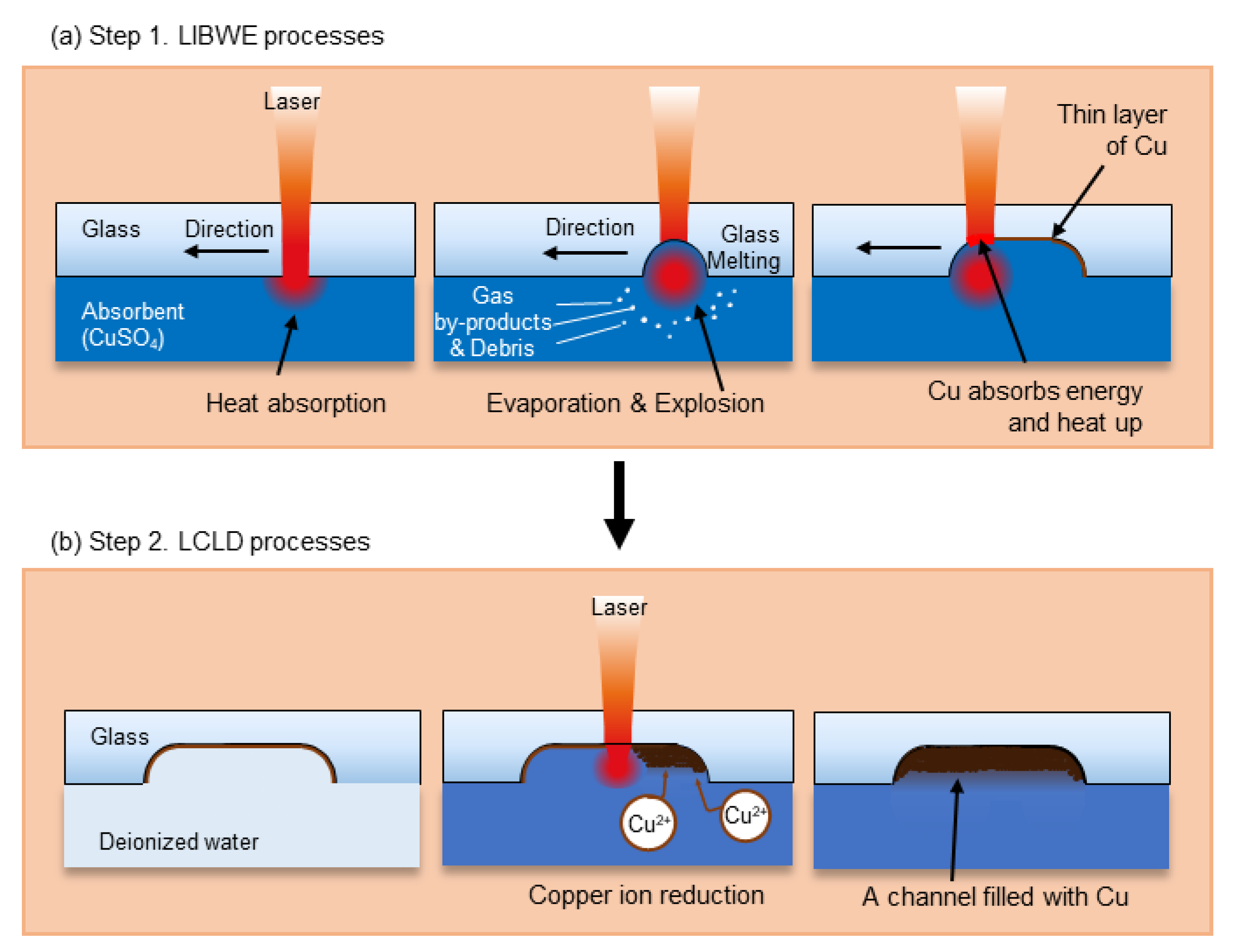
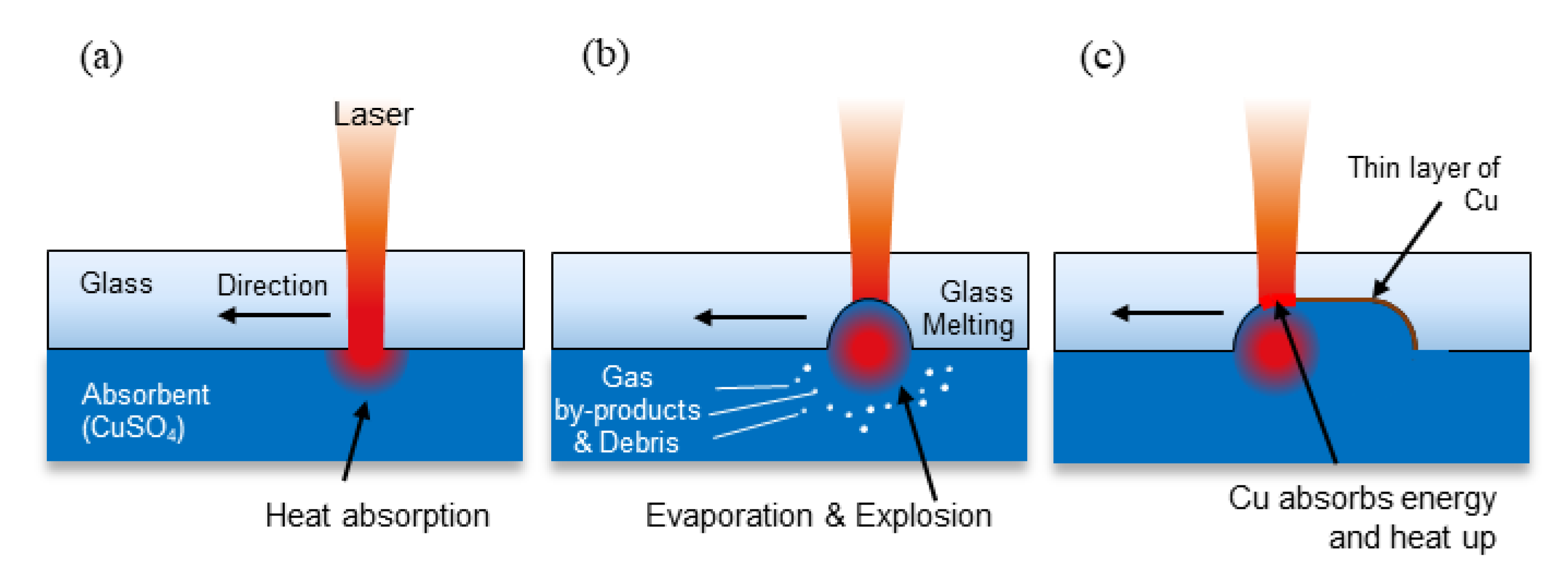
2.1. Laser-Induced Backside Wet Etching
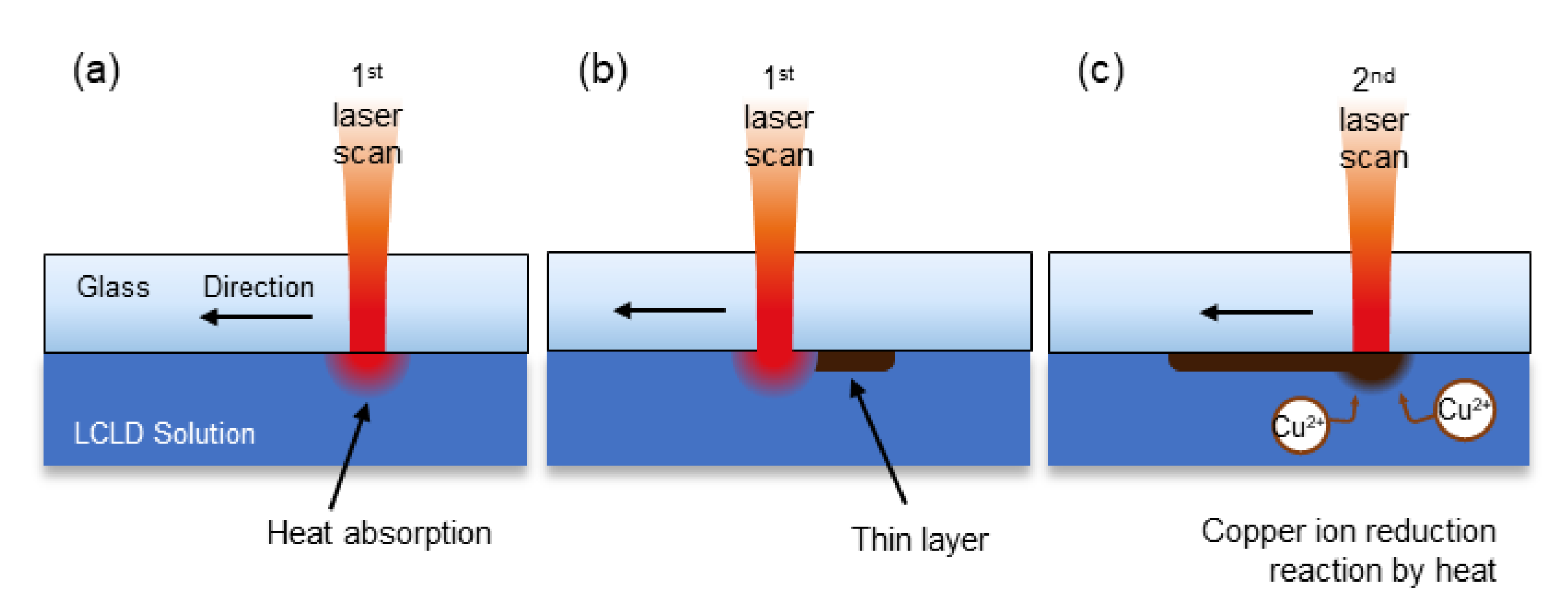
2.2. Laser-Induced Chemical Liquid Phase Deposition
3. Materials and Methods
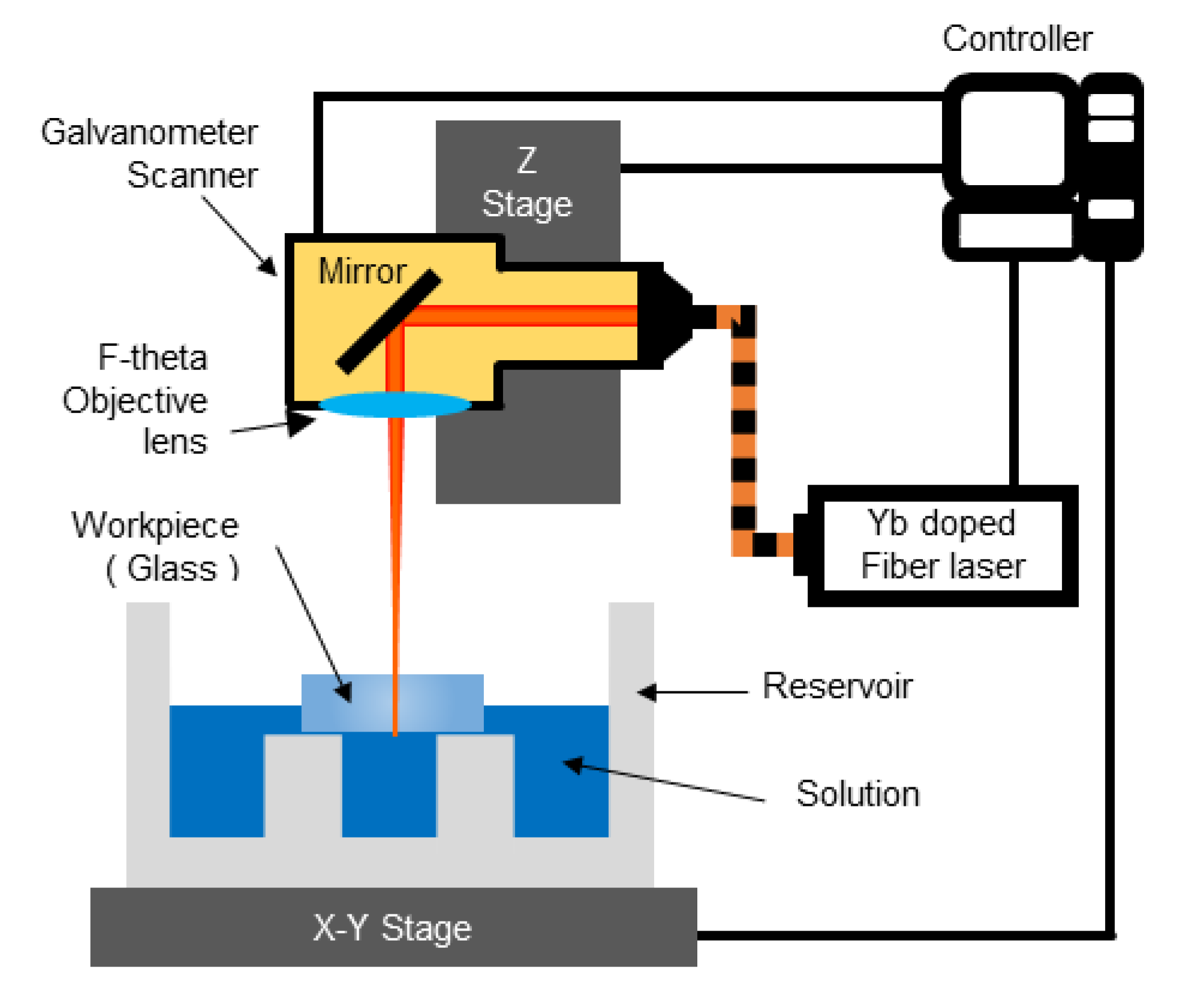
3.1. Experimental Devices and Materials
3.2. Experimental Procedures
4. Results and Discussion
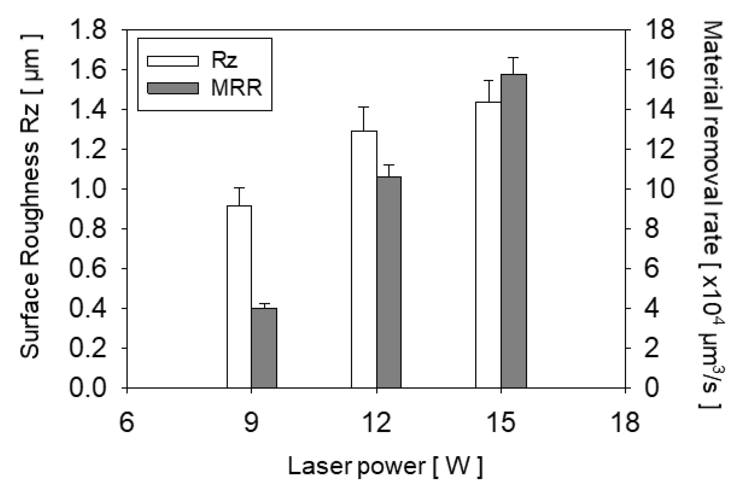
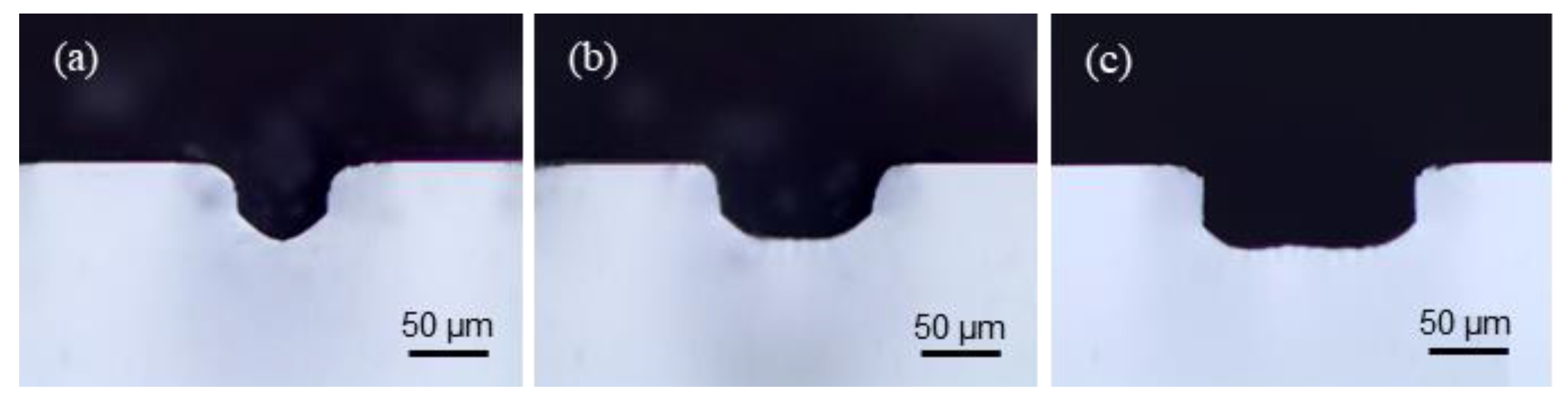
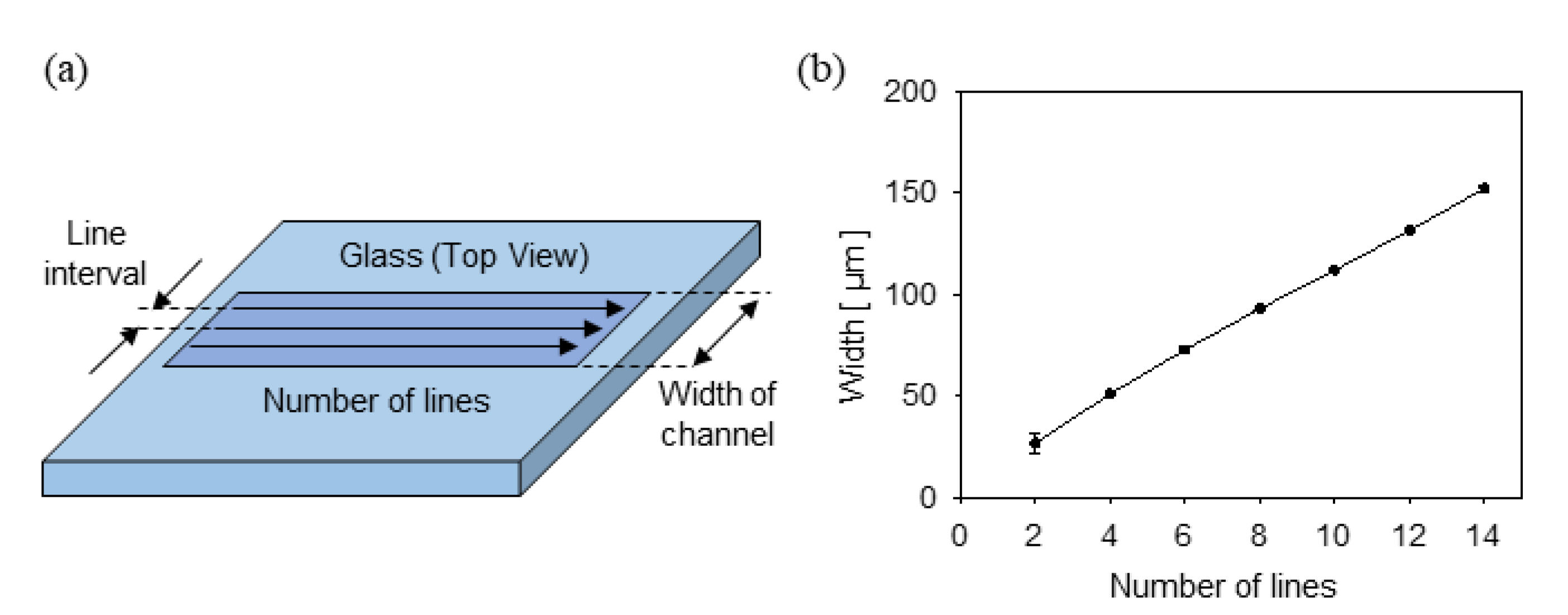
4.1. Fabrication of Channels by LIBWE
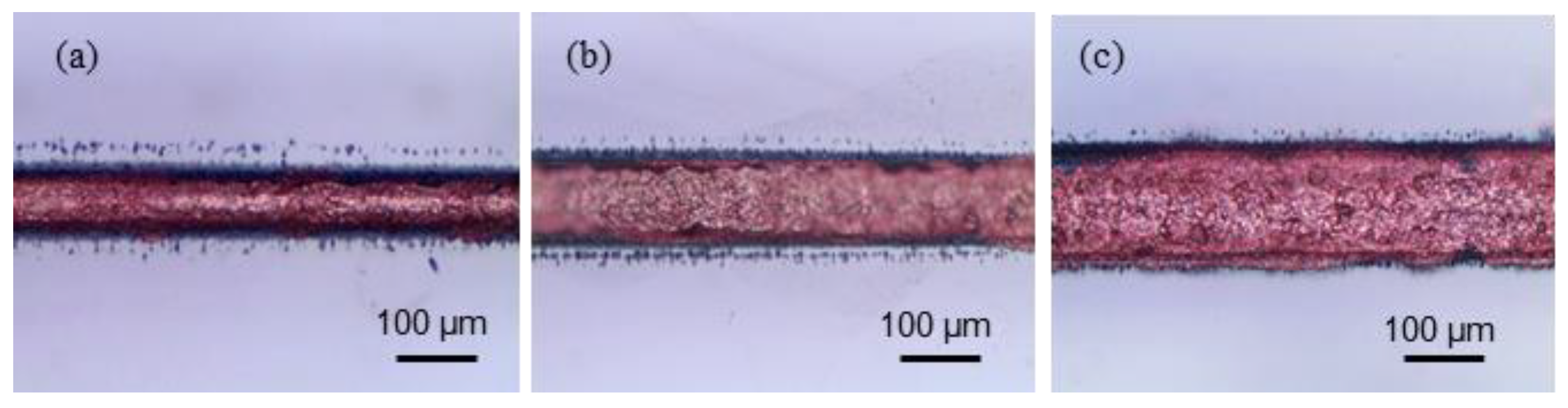
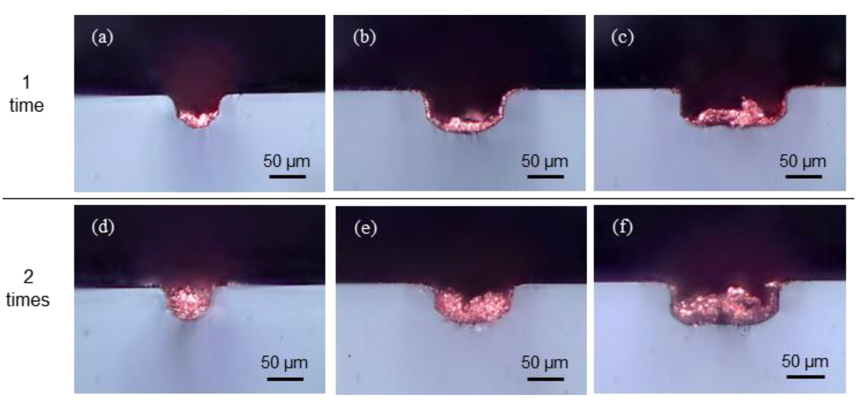
4.2. Laser Copper Deposition Inside of Channels
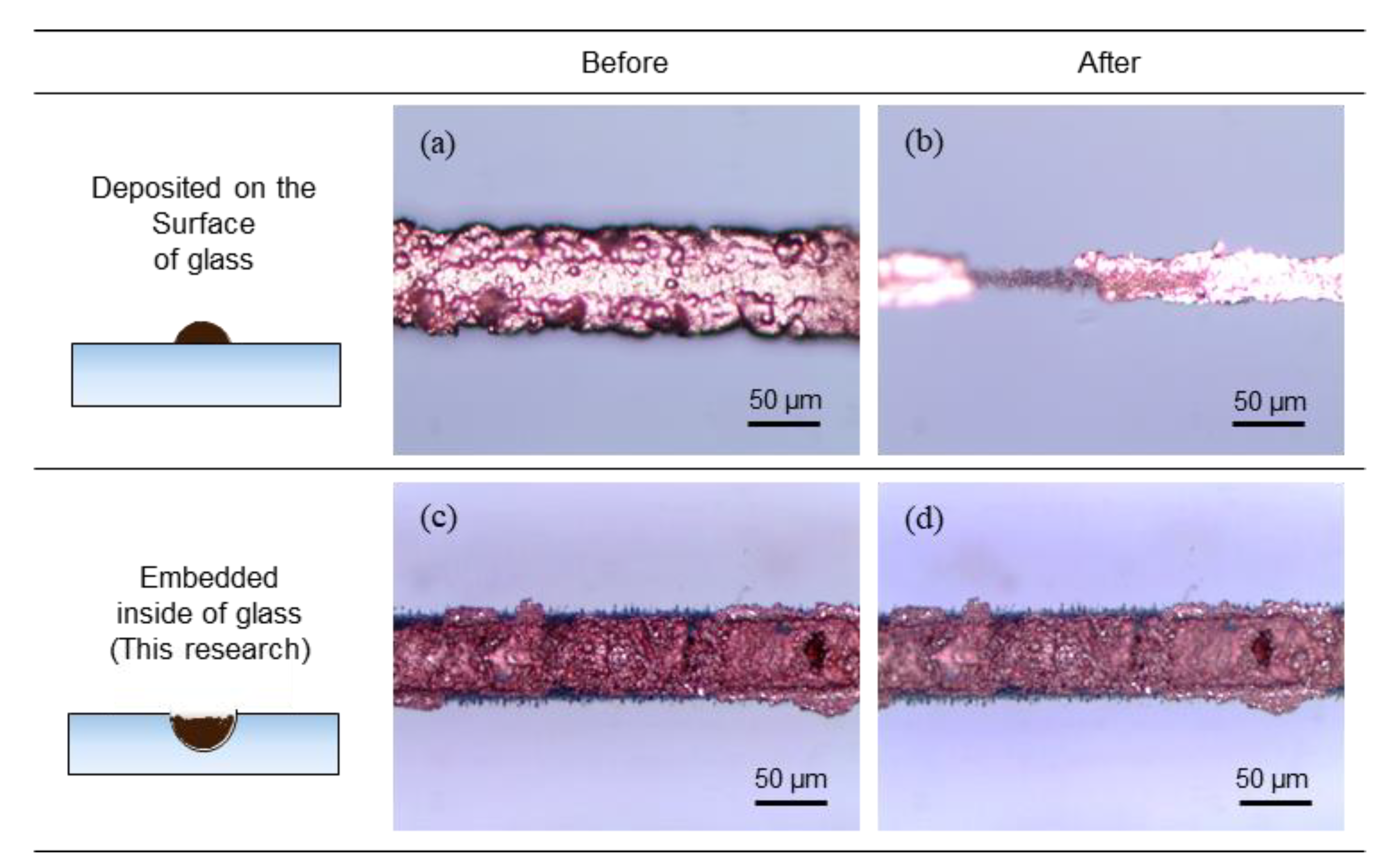
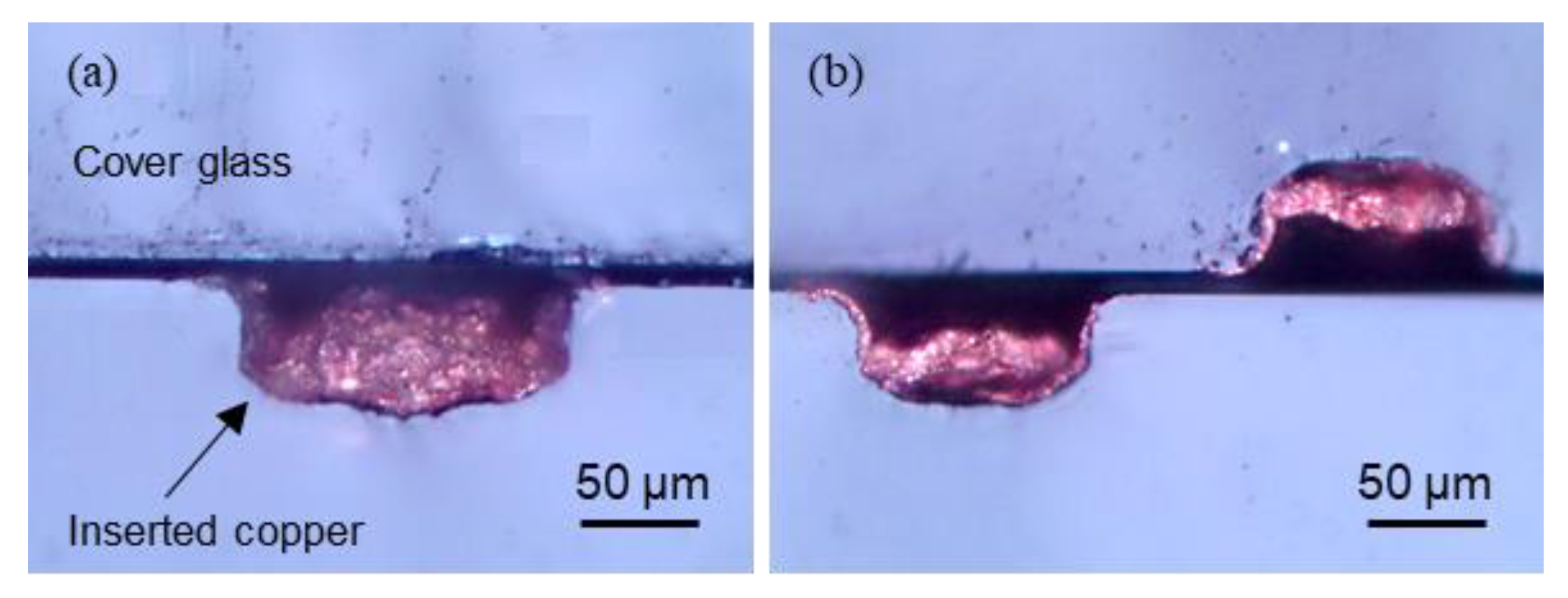
4.3. Durability of Deposited Copper
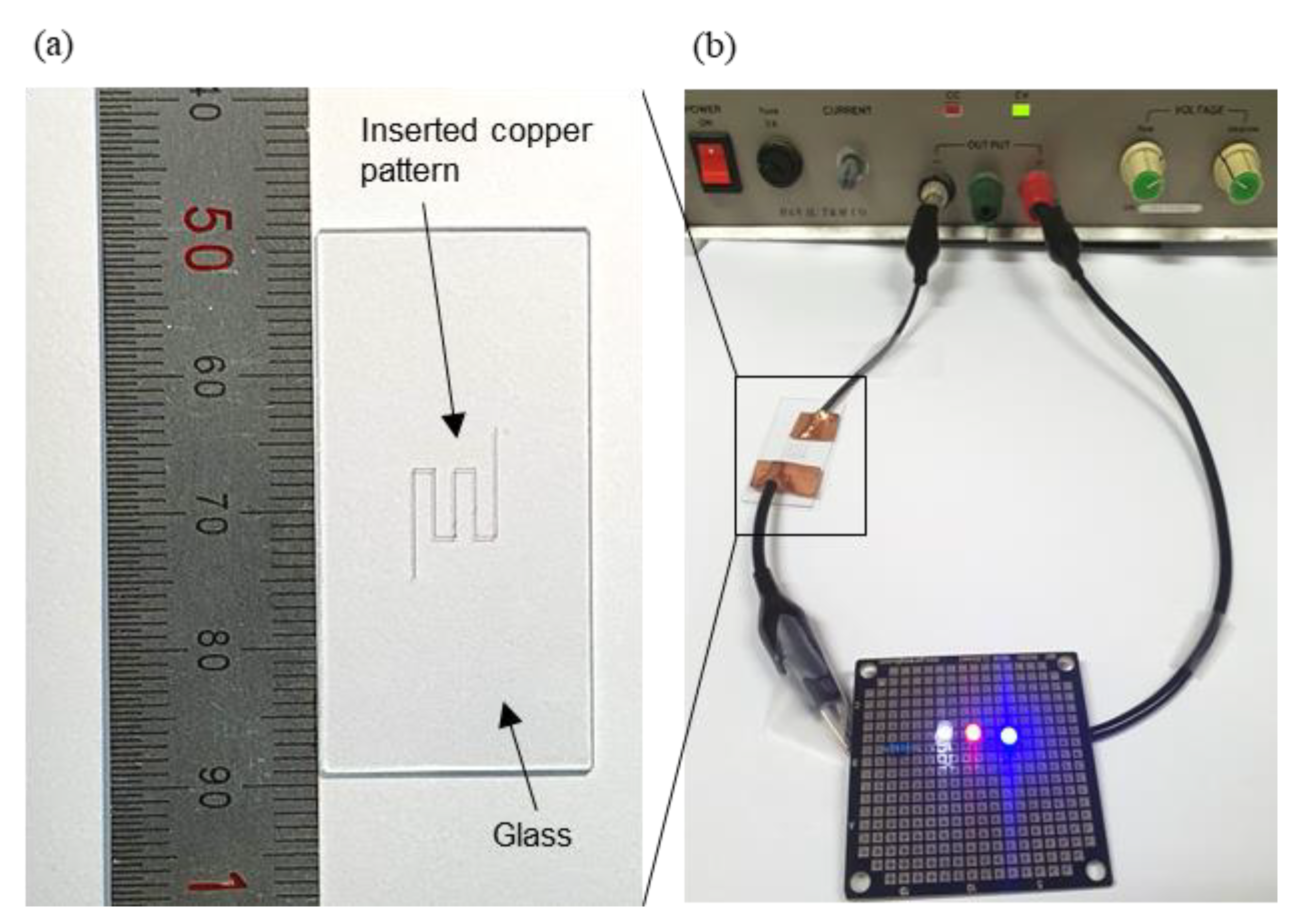
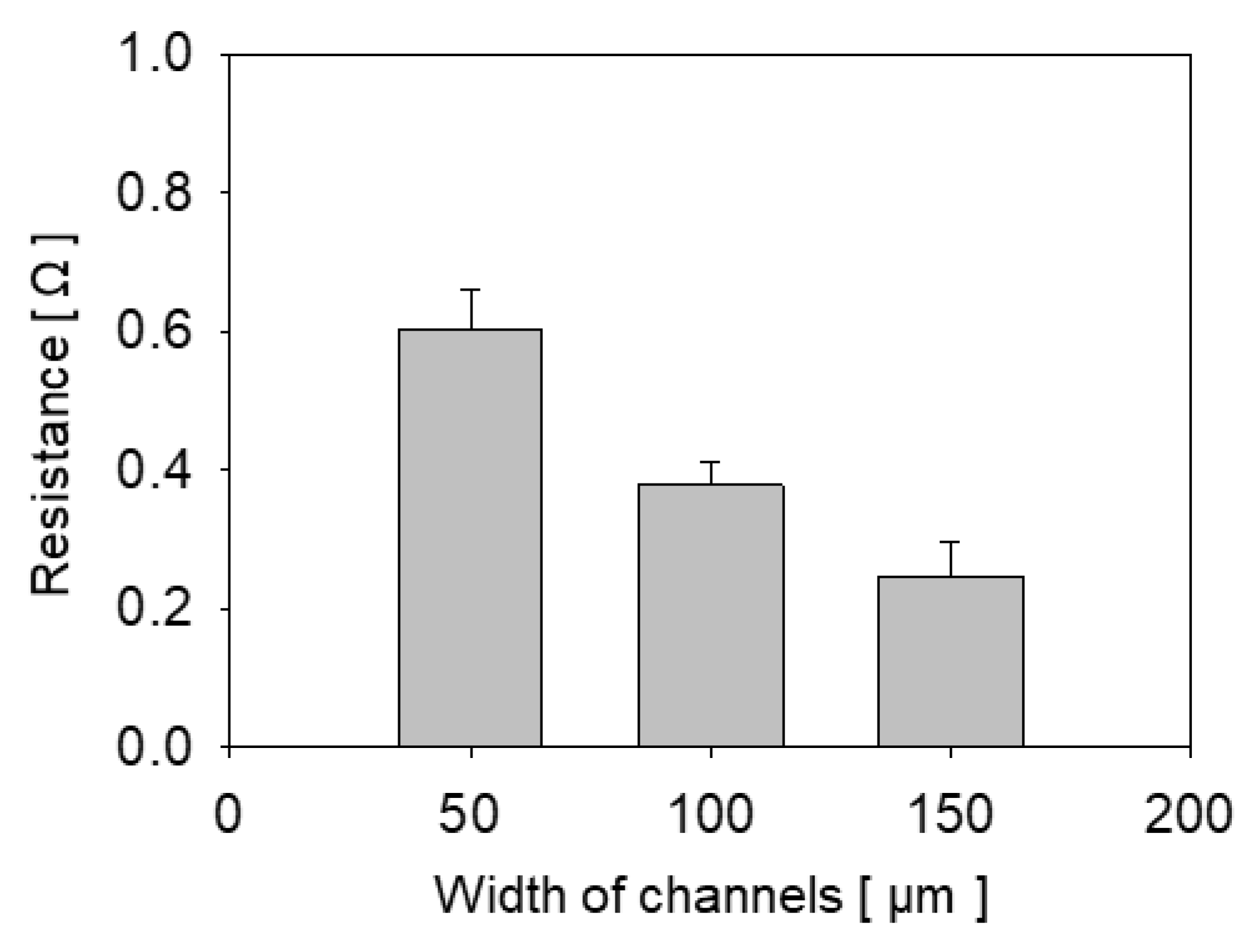
4.4. Conductivity and Applications
5. Conclusions
Author Contributions
Funding
Conflicts of Interest
References
- Moqadam, S.I.; Mädler, L.; Ellendt, N. A high temperature drop-on-demand droplet generator for metallic melts. Micromachines 2019, 10, 1–12. [Google Scholar]
- Wu, Y.; Du, J.; Choy, K.L.; Hench, L.L. Laser densification of alumina powder beds generated using aerosol assisted spray deposition. J. Eur. Ceram. Soc. 2007, 27, 4727–4735. [Google Scholar] [CrossRef]
- Quinto, D.T.; Wolfe, G.J.; Jindal, P.C. High temperature microhardness of hard coatings produced by physical and chemical vapor deposition. Thin Solid Films 1987, 153, 19–36. [Google Scholar] [CrossRef]
- Crawford, W.J. Verb agreement and disagreement. J. Engl. Linguist. 2005, 33, 35–61. [Google Scholar] [CrossRef]
- Han, M.J.; Khang, D.Y. Glass and plastics platforms for foldable electronics and displays. Adv. Mater. 2015, 27, 4969–4974. [Google Scholar] [CrossRef] [PubMed]
- Kim, J.G.; Nam, K.G.; Cho, S.H.; Chang, W.S.; Na, S.J.; Whang, K.H. Micromachining characteristics inside transparent materials using femtosecond laser pulses. J. Korean Soc. Precis. Eng. 2006, 23, 190–196. [Google Scholar]
- Zehnder, S.; Schwaller, P.; von Arx, U.; Neuenschwander, B. Laser-induced chemical liquid-phase deposition of copper on transparent substrates. In Proceedings of the International Conference on Advanced Laser Technologies, Thun, Switzerland, 2–6 September 2012. [Google Scholar]
- Chen, M.F.; Chen, Y.P.; Hsiao, W.T.; Gu, Z.P. Laser direct write patterning technique of indium tin oxide film. Thin Solid Films 2007, 515, 8515–8518. [Google Scholar] [CrossRef]
- Wang, M.W.; Liu, T.Y.; Pang, D.C.; Hung, J.C.; Tseng, C.C. Inkjet printing of a PH sensitive palladium catalyst patterns of ITO glass for electroless copper. Surf. Coat. Technol. 2014, 259, 340–345. [Google Scholar] [CrossRef]
- Sugioka, K.; Masuda, M.; Hongo, T.; Cheng, Y.; Shihoyama, K.; Midorikawa, K. Three-dimensional microfluidic structure embedded in photostructurable glass by femtosecond laser for lab-on-chip applications. Appl. Phys. A Mater. Sci. Process. 2004, 79, 815–817. [Google Scholar] [CrossRef]
- Hanada, Y.; Sugioka, K.; Midorikawa, K. Selective metallization of photostructurable glass by femtosecond laser direct writing for biochip application. Appl. Phys. A Mater. Sci. Process. 2008, 90, 603–607. [Google Scholar] [CrossRef]
- Deckert, C.A. Electroless copper plating. A review: Part I. Plat. Surf. Finish. 1995, 82, 58–64. [Google Scholar]
- Honma, H.; Kobayashi, T. Electroless copper deposition process using glyoxylic acid as a reducing agent. J. Electrochem. Soc. 1994, 141, 730–733. [Google Scholar] [CrossRef]
- Kim, H.G.; Park, M.S. Circuit patterning using laser on transparent material. Surf. Coat. Technol. 2017, 315, 377–384. [Google Scholar] [CrossRef]
- Long, J.; Li, J.; Li, M.; Xie, X. Fabrication of robust metallic micropatterns on glass surfaces by selective metallization in laser-induced porous surface structures. Surf. Coat. Technol. 2019, 374, 338–344. [Google Scholar] [CrossRef]
- Kordas, K.; Bali, K.; Nanai, L.; Galbacs, G.; Uusimaki, A.; Leppavuori, S. Reaction dynamics of CW ar laser induced copper direct writing from liquid electrolyte on polyimide substrates. Appl. Surf. Sci. 2000, 158, 127–133. [Google Scholar] [CrossRef]
- Manshina, A.A.; Povolotskiy, A.V.; Ivanova, T.Y.; Tver’Yanovich, Y.S.; Tunik, S.P.; Kim, D.; Kim, M.; Kwon, S.C. Effect of salt precursor on laser-assisted copper deposition. Appl. Phys. A Mater. Sci. Process. 2007, 89, 755–759. [Google Scholar] [CrossRef]
- Chen, Q.J.; Imen, K.; Allen, S.D. Laser enhanced electroless plating of micron-scale copper wires. J. Electrochem. Soc. 2000, 147, 1418. [Google Scholar] [CrossRef]
- Kochemirovsky, V.A.; Skripkin, M.Y.; Tveryanovich, Y.S.; Mereshchenko, A.S.; Gorbunov, A.O.; Panov, M.S.; Tumkin, I.I.; Safonov, S.V. Laser-induced copper deposition from aqueous and aqueous-organic solutions: State of the art and prospects of research. Russ. Chem. Rev. 2015, 84, 1059–1075. [Google Scholar] [CrossRef]
- Tumkin, I.I.; Kochemirovsky, V.A.; Bal’makov, M.D.; Safonov, S.V.; Zhigley, E.S.; Logunov, L.S.; Shishkova, E.V. Laser-induced deposition of nanostructured copper microwires on surfaces of composite materials. Surf. Coat. Technol. 2015, 264, 187–192. [Google Scholar] [CrossRef]
- Wang, X.C.; Zheng, H.Y.; Lim, G.C. Laser induced copper electroless plating on polyimide with Q-switch Nd:YAG laser. Appl. Surf. Sci. 2002, 200, 165–171. [Google Scholar] [CrossRef]
- Seo, J.M. Fabrication of Embedded Copper Wire on Glass by Laser-Induced Chemical Liquid Phase Deposition with Ytterbium Fiber Laser. Master’s Thesis, Seoul National University, Seoul, Korea, 2020. [Google Scholar]
- Kwon, K.-K.; Kim, H.; Kim, T.; Chu, C.N. High Aspect ratio channel fabrication with near-infrared laser-induced backside wet etching. J. Mater. Process. Technol. 2020, 278, 116505. [Google Scholar] [CrossRef]
- Huang, Z.Q.; Hong, M.H.; Do, T.B.M.; Lin, Q.Y. Laser etching of glass substrates by 1064 Nm Laser irradiation. Appl. Phys. A Mater. Sci. Process. 2008, 93, 159–163. [Google Scholar] [CrossRef]
- Kawaguchi, Y.; Ding, X.; Narazaki, A.; Sato, T.; Niino, H. Transient pressure induced by laser ablation of toluene, a highly laser-absorbing liquid. Appl. Phys. A Mater. Sci. Process. 2005, 80, 275–281. [Google Scholar] [CrossRef]
- Xie, X.; Huang, X.; Jiang, W.; Wei, X.; Hu, W.; Ren, Q. Three dimensional material removal model of laser-induced backside wet etching of sapphire substrate with CuSO4 solutions. Opt. Laser Technol. 2017, 89, 59–68. [Google Scholar] [CrossRef]
- Bugaev, S.P.; Sochugov, N.S. Production of large-area coatings on glasses and plastics. Surf. Coat. Technol. 2000, 131, 474–480. [Google Scholar] [CrossRef]
- Chong, E.K.; Stevens, M.G.; Nissen, K.E. Effect of surface roughness on the adhesion of electrolessly plated platinum to poly(ethylene terephthalate) films. J. Adhes. 2003, 79, 667–681. [Google Scholar] [CrossRef]
- Okamoto, N.; Wang, F.; Watanabe, T. Adhesion of electrodeposited copper, nickel and silver films on copper, nickel and silver substrates. Mater. Trans. 2004, 45, 3330–3333. [Google Scholar] [CrossRef] [Green Version]
- Kochemirovsky, V.A.; Menchikov, L.G.; Kuz’Min, A.G.; Safonov, S.V.; Tumkin, I.I.; Tver’Yanovich, Y.S. Side reactions during laser-induced deposition of copper from aqueous solutions of cuii complexes. Russ. Chem. Bull. 2012, 61, 1041–1047. [Google Scholar] [CrossRef]
- Kochemirovsky, V.A.; Fateev, S.A.; Logunov, L.S.; Tumkin, I.I.; Safonov, S.V. Laser-induced copper deposition with weak reducing agents. Int. J. Electrochem. Sci. 2014, 9, 644–658. [Google Scholar]
- Hanna, F.; Abdel Hamid, Z.; Abdel Aal, A. Controlling factors affecting the stability and rate of electroless copper plating. Mater. Lett. 2004, 58, 104–109. [Google Scholar] [CrossRef]
- Kim, S.; Kim, J.; Joung, Y.H.; Choi, J.; Koo, C. Bonding strength of a glass microfluidic device fabricated by femtosecond laser micromachining and direct welding. Micromachines 2018, 9, 639. [Google Scholar] [CrossRef] [PubMed] [Green Version]
- Alkire, R.C.; Romankiw, L.T. Plating of copper into through-holes and vias. J. Electrochem. Soc. 1989, 136, 206–215. [Google Scholar]


| Variables | Values |
|---|---|
| Laser power [W] | 9, 12, 15, 18 |
| Scan speed [mm/s] | 150 |
| Repetition rate of pulsed laser [kHz] | 50 |
| Scan length [mm] | 2 |
| Number of repeated laser scan | 500, 800, 2000 |
| Line interval [µm] | 10 |
| Number of lines | 4, 9, 14 |
| Variables | Values |
|---|---|
| Laser power [W] | 2, 3, 4 |
| Scan speed [mm/s] | 0.015 |
| Repetition rate of pulsed laser [kHz] | 80 |
| Scan length [mm] | 2 |
| Number of laser scan | 1, 2 |
| Area | Measured Surface Roughness | Area | Detection of Cu | |
|---|---|---|---|---|
| Rz (µm) | Ra (µm) | |||
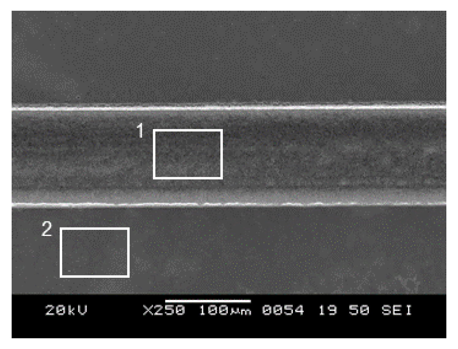
| Bottom of channel | 1.44 | 0.30 | Square 1 | O |
| Surface of glass | 0.05 | 0.01 | Square 2 | X |
© 2020 by the authors. Licensee MDPI, Basel, Switzerland. This article is an open access article distributed under the terms and conditions of the Creative Commons Attribution (CC BY) license (http://creativecommons.org/licenses/by/4.0/).
Share and Cite
Seo, J.M.; Kwon, K.-K.; Song, K.Y.; Chu, C.N.; Ahn, S.-H. Deposition of Durable Micro Copper Patterns into Glass by Combining Laser-Induced Backside Wet Etching and Laser-Induced Chemical Liquid Phase Deposition Methods. Materials 2020, 13, 2977. https://doi.org/10.3390/ma13132977
Seo JM, Kwon K-K, Song KY, Chu CN, Ahn S-H. Deposition of Durable Micro Copper Patterns into Glass by Combining Laser-Induced Backside Wet Etching and Laser-Induced Chemical Liquid Phase Deposition Methods. Materials. 2020; 13(13):2977. https://doi.org/10.3390/ma13132977
Chicago/Turabian StyleSeo, Jae Min, Kui-Kam Kwon, Ki Young Song, Chong Nam Chu, and Sung-Hoon Ahn. 2020. "Deposition of Durable Micro Copper Patterns into Glass by Combining Laser-Induced Backside Wet Etching and Laser-Induced Chemical Liquid Phase Deposition Methods" Materials 13, no. 13: 2977. https://doi.org/10.3390/ma13132977