Influence Mechanism of Cu Layer Thickness on Photoelectric Properties of IWO/Cu/IWO Films


Abstract
1. Introduction
2. Materials and Methods
3. Results and Discussion
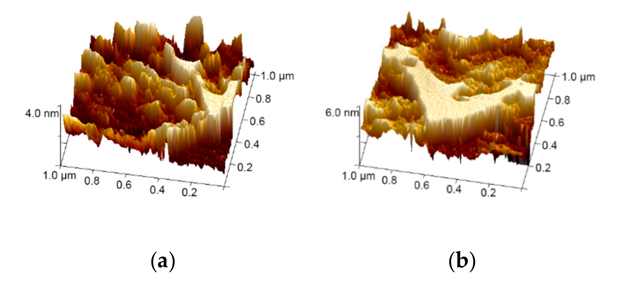
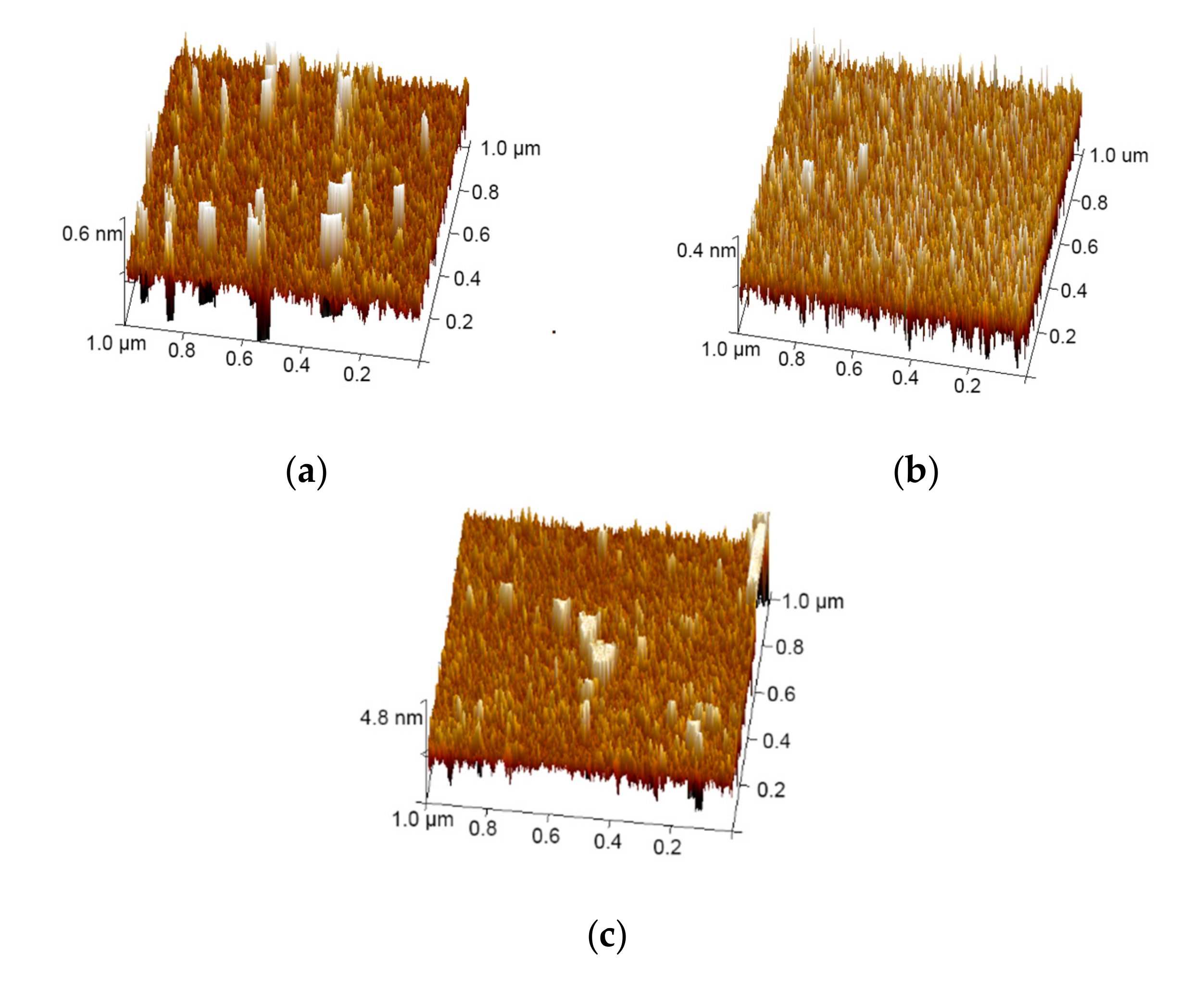
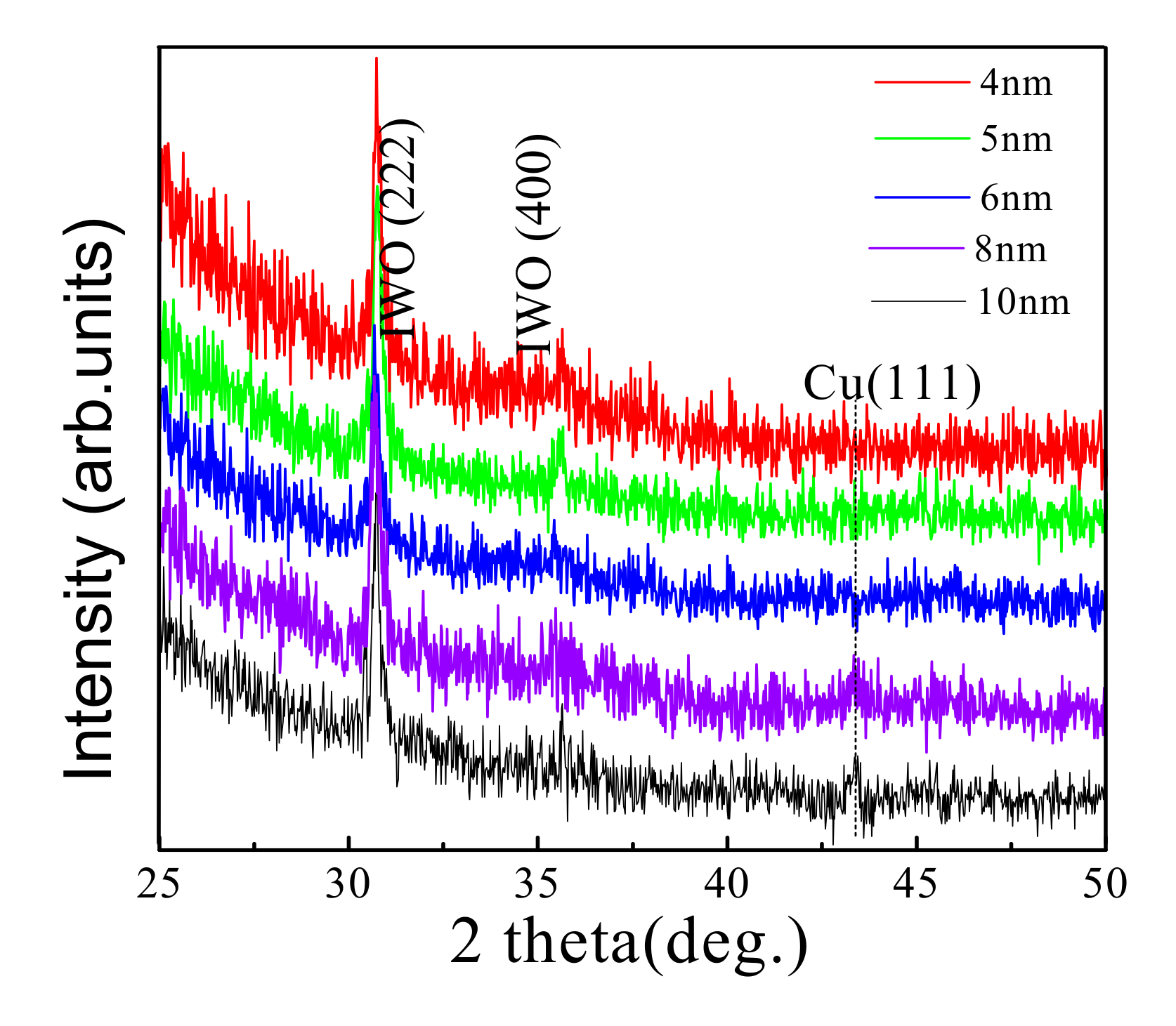
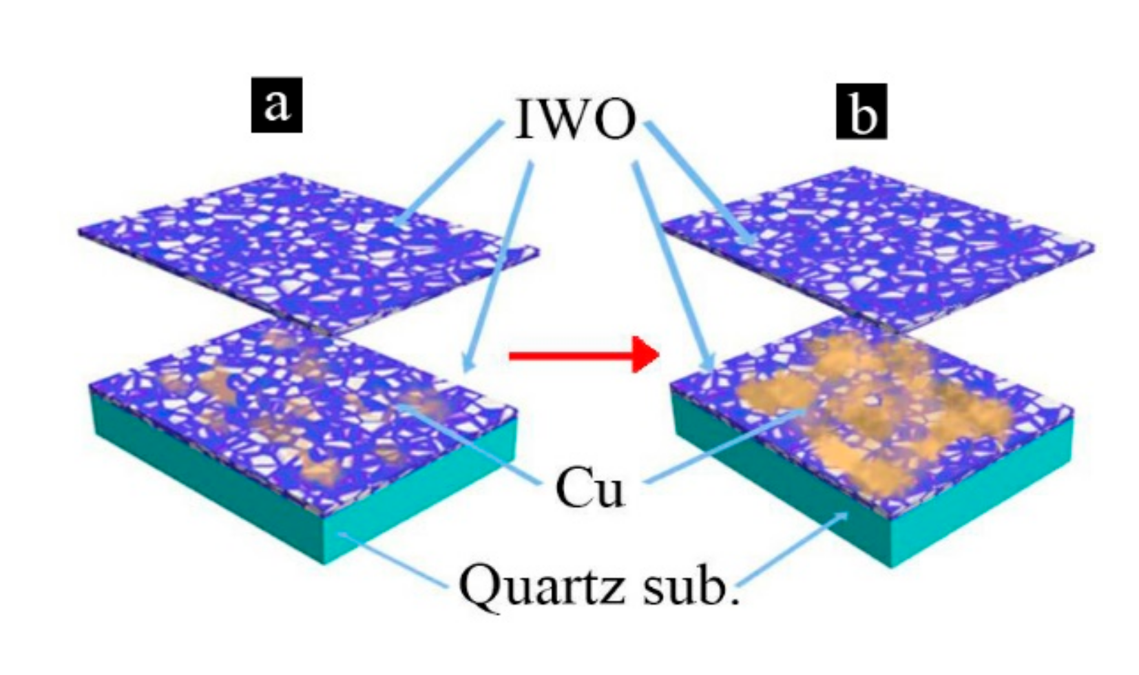
3.1. Morphology and Structure
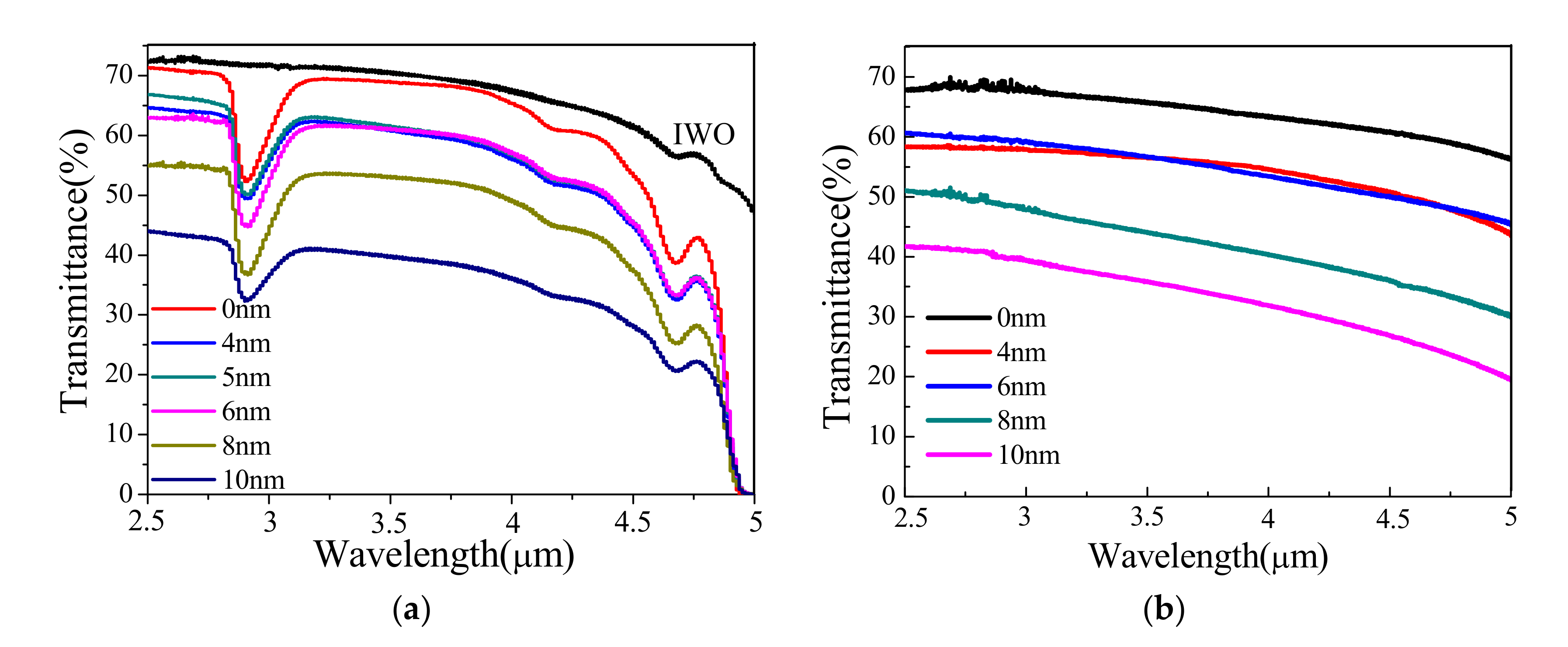
3.2. Optical Properties
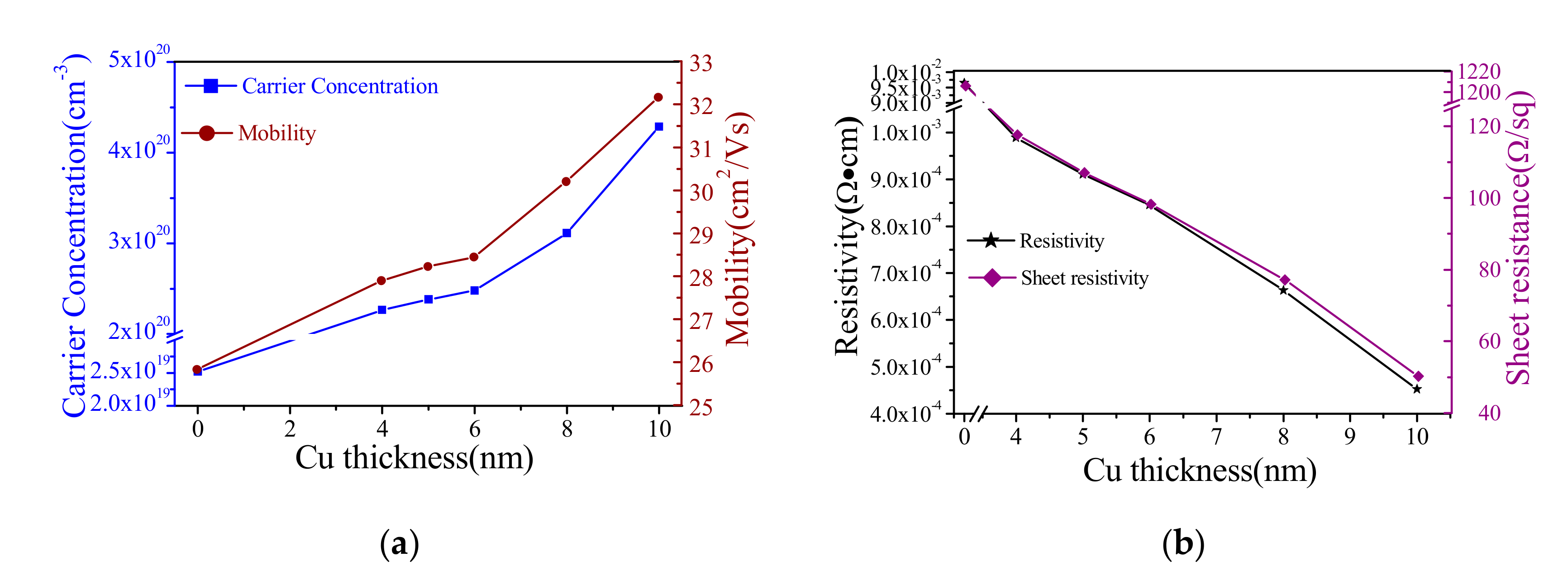
3.3. Electrical Properties
4. Conclusions
Author Contributions
Funding
Conflicts of Interest
References
- Nomura, K.; Ohta, H.; Ueda, K.; Kamiya, T.; Hirano, M.; Hosono, H. Thin-film transistor fabricated in single-crystalline transparent oxide semiconductor. Science 2003, 300, 1269–1272. [Google Scholar] [CrossRef] [PubMed]
- Zhang, K.H.L.; Egdell, R.G.; Offi, F.; Iacobucci, S.; Petaccia, L.; Gorovikov, S.; King, P.D.C. Microscopic origin of electron accumulation in In2O3. Phys. Rev. Lett. 2013, 110, 056803. [Google Scholar] [CrossRef] [PubMed]
- Lu, X.; Chen, A.; Luo, Y.; Lu, P.; Dai, Y.; Enriquez, E.; Dowden, P.; Xu, H.; Kotula, P.G.; Azad, A.K.; et al. Conducting interface in oxide homojunction: understanding of superior properties in black TiO2. Nano Lett. 2016, 16, 5751–5755. [Google Scholar] [CrossRef] [PubMed]
- Parthiban, S.; Gokulakrishnan, V.; Elangovan, E.; Goncalves, G.; Ramamurthi, K.; Fortunato, E.; Martins, R. High mobility and visible-near infrared transparent titanium doped indium oxide thin films produced by spray pyrolysis. Thin Solid Films 2012, 524, 268–271. [Google Scholar] [CrossRef]
- Huang, W.; Zhu, B.; Chang, S.Y.; Zhu, S.; Cheng, P.; Hsieh, Y.T.; Meng, L.; Wang, R.; Wang, C.; Zhu, C.; et al. High mobility indium oxide electron transport layer for an efficient charge extraction and optimized nanomorphology in organic photovoltaics. Nano Lett. 2018, 18, 5805–5811. [Google Scholar] [CrossRef] [PubMed]
- Janotti, A.; Van de Walle, C.G. Fundamentals of zinc oxide as a semiconductor. Rep. Prog. Phys. 2009, 72, 126501. [Google Scholar] [CrossRef]
- Cheng, Y.; Zhang, X.; Che, L.; Chen, J.; Jing, B.; Sun, R.; Luo, X. Binding energy of Sb-related complex in p-doped ZnO film. J. Alloys Compd. 2019, 800, 219–223. [Google Scholar] [CrossRef]
- Kolhe, P.S.; Shinde, A.B.; Kulkarni, S.G.; Maiti, N.; Koinkar, P.M.; Sonawane, K.M. Gas sensing performance of Al doped ZnO thin film for H2S detection. J. Alloys Compd. 2018, 748, 6–11. [Google Scholar] [CrossRef]
- Shivashankar, E.; Elangovan, S.A.; Ramamurthi, K. Studies on structural and electrical properties of sprayed SnO2: Sb films. J. Cryst. Growth 2005, 276, 215–221. [Google Scholar] [CrossRef]
- Huang, Y.; Zhang, Q.; Li, G. Transparent conductive tungsten-doped tin oxide polycrystalline films prepared on quartz substrates. Semicond. Sci. Technol. 2009, 24, 015003. [Google Scholar] [CrossRef]
- Parthiban, S.; Gokulakrishnan, V.; Ramamurthi, K.; Elangovan, E.; Martins, R.; Fortunato, E.; Ganesan, R. High near-infrared transparent molybdenum-doped indium oxide thin films for nanocrystalline silicon solar cell applications. Sol. Energy Mater. Sol. Cells 2009, 93, 92–97. [Google Scholar] [CrossRef]
- Meng, F.; Shi, J.; Liu, Z.; Cui, Y.; Lu, Z.; Feng, Z. High mobility transparent conductive W-doped In2O3 thin films prepared at low substrate temperature and its application to solar cells. Sol. Energy Mater. Sol. Cells 2014, 122, 70–74. [Google Scholar] [CrossRef]
- Lu, X.J.; Mou, X.L.; Wu, J.J.; Zhang, D.W.; Zhang, L.L.; Huang, F.Q.; Xu, F.F.; Huang, S.M. Improved-performance dye-sensitized solar cells using Nb-doped TiO2 electrodes: Efficient electron injection and transfer. Adv. Funct. Mater. 2010, 20, 509–515. [Google Scholar] [CrossRef]
- Kim, M.J.; Kim, H.G.; Kim, S.S. Composite layer formation on plastic substrates for flexible display by using functionalized nanoclay. Macromol. Res. 2012, 20, 739–745. [Google Scholar] [CrossRef]
- Cho, S.-W.; Jeong, J.-A.; Bae, J.-H.; Moon, J.-M.; Choi, K.-H.; Jeong, S.W.; Park, N.-J.; Kim, J.-J.; Lee, S.H.; Kang, J.-W.; et al. Highly flexible, transparent, and low resistance indium zinc oxide-Ag-indium zinc oxide multilayer anode on polyethylene terephthalate substrate for flexible organic light-emitting diodes. Thin Solid Films 2008, 516, 7881–7885. [Google Scholar] [CrossRef]
- Ryu, S.Y.; Jo, S.J.; Kim, C.S.; Choi, S.H.; Noh, J.H.; Baik, H.K.; Jeong, H.S.; Han, D.W.; Song, S.Y.; Lee, K.S. Transparent organic light-emitting diodes using resonant tunneling double barrier structures. Appl. Phys. Lett. 2007, 91, 093515. [Google Scholar] [CrossRef]
- Kumar, N.; Arora, K.; Kumar, M. High performance, flexible and room temperature grown amorphous Ga2O3 solar-blind photodetector with amorphous indium-zinc-oxide transparent conducting electrodes. J. Phys. D Phys. 2019, 5, 335103. [Google Scholar] [CrossRef]
- Faber, H.; Das, S.; Lin, Y.-H.; Pliatsikas, N.; Zhao, K.; Kehagias, T.; Dimitrakopulos, G.; Amassian, A.; Patsalas, P.A.; Anthopoulos, T.D. Heterojunction oxide thin-film transistors with unprecedented electron mobility grown from solution. Sci. Adv. 2017, 3, 1602640. [Google Scholar] [CrossRef]
- Nomura, K.; Ohta, H.; Takagi, A.; Kamiya, T.; Hirano, M.; Hosono, H. Room-temperature fabrication of transparent flexible thin-film transistors using amorphous oxide semiconductors. Nature 2004, 432, 488–492. [Google Scholar] [CrossRef]
- Adamopoulos, G.; Thomas, S.; Wobkenberg, P.H.; Bradley, D.D.C.; McLachlan, M.A.; Anthopoulos, T.D. High-mobility low-voltage ZnO and Li-doped ZnO transistors Based on ZrO2 high-k dielectric grown by spray pyrolysis in ambient air. Adv. Mater. 2011, 23, 1894. [Google Scholar] [CrossRef]
- Zhang, L.; Zhou, Y.; Guo, L.; Zhao, W.; Barnes, A.; Zhang, H.T.; Eaton, C.; Zheng, Y.; Brahlek, M.; Haneef, H.F. Correlated metals as transparent conductors. Nat. Mater. 2016, 15, 204–210. [Google Scholar] [CrossRef] [PubMed]
- Guo, S.; Yang, L.; Dai, B.; Geng, F.; Yang, Z.; Lei, P.; Wang, P.; Gao, G.; Han, J.; Ralchenko, V. Hydrated magnesium-carbon films with conductivity and wide-range visible-to-far-infrared transparency. Mater. Lett. 2018, 216, 88–91. [Google Scholar] [CrossRef]
- Ellmer, K. Past achievements and future challenges in the development of optically transparent electrodes. Nat. Photonics 2012, 6, 809–817. [Google Scholar] [CrossRef]
- Bhosle, V.; Prater, J.T.; Yang, F.; Burk, D.; Forrest, S.R.; Narayan, J. Gallium-doped zinc oxide films as transparent electrodes for organic solar cell applications. J. Appl. Phys. 2007, 102. [Google Scholar] [CrossRef]
- Guillén, C.; Herrero, J. TCO/metal/TCO structures for energy and flexible electronics. Thin Solid Films 2011, 520, 1–17. [Google Scholar] [CrossRef]
- Ryu, S.Y.; Noh, J.H.; Hwang, B.H.; Kim, C.S.; Jo, S.J.; Kim, J.T.; Hwang, H.S.; Baik, H.K.; Jeong, H.S.; Lee, C.H.; et al. Transparent organic light-emitting diodes consisting of a metal oxide multilayer anode. Appl. Phys. Lett. 2008, 92, 15. [Google Scholar] [CrossRef]
- Wu, H.-W.; Yang, R.-Y.; Hsiung, C.-M.; Chu, C.-H. Influence of Ag thickness of aluminum-doped ZnO/Ag/aluminum-doped ZnO thin films. Thin Solid Films 2012, 520, 7147–7152. [Google Scholar] [CrossRef]
- Sahu, D.R.; Lin, S.-Y.; Huang, J.-L. Investigation of conductive and transparent Al-doped ZnO/Ag/Al-doped ZnO multilayer coatings by electron beam evaporation. Thin Solid Films 2008, 516, 4728–4732. [Google Scholar] [CrossRef]
- Crupi, I.; Boscarino, S.; Strano, V.; Mirabella, S.; Simone, F.; Terrasi, A. Optimization of ZnO:Al/Ag/ZnO:Al structures for ultra-thin high-performance transparent conductive electrodes. Thin Solid Films 2012, 520, 4432–4435. [Google Scholar] [CrossRef]
- Hu, J.; Gordon, R.G. Textured aluminum-doped zine oxide thin films from atmospheric pressure chemical-vapor deposition. J. Appl. Phys. 1992, 71, 880–890. [Google Scholar] [CrossRef]
- Mass, J.; Bhattacharya, P.; Katiyar, R.S. Effect of high substrate temperature on Al-doped ZnO thin films grown by pulsed laser deposition. Mater. Sci. Eng. B 2003, 103, 9–15. [Google Scholar] [CrossRef]
- Lozano, O.; Chen, Q.Y.; Wadekar, P.V.; Seo, H.W.; Chinta, P.V.; Chu, L.H.; Tu, L.W.; Lo, I.; Yeh, S.W.; Ho, N.J.; et al. Factors limiting the doping efficiency of transparent conductors: A case study of Nb-doped In2O3 epitaxial thin-films. Sol. Energy Mater. Sol. Cells 2013, 113, 171–178. [Google Scholar] [CrossRef]
- Dong, D.; Wang, W.; Zhang, F.; Fu, Q.; Pan, J. Preparation and characterization of micro-grid modified In2O3: W films. Thin Solid Films 2016, 612, 1–7. [Google Scholar] [CrossRef]
- Günther, C.; Günther, S.; Kopatzki, E. Microscopic Aspects of Thin Metal Film Epitaxial Growth on Metallic Substrates. Ber. Bunsenges. Phys. Chem. 1993, 97, 522–537. [Google Scholar] [CrossRef]
- Zhang, D.; Yabe, H.; Akita, E.; Wang, P.; Murakami, R.; Song, X. Effect of silver evolution on conductivity and transmittance of ZnO/Ag thin films. J. Appl. Phys. 2011, 109, 104318. [Google Scholar] [CrossRef]
- Kreibig, U.; Fragstein, C.V. The Limitation of Electron Mean Free Path in Small Silver Particles. Z. Phys. 1969, 224, 307–323. [Google Scholar] [CrossRef]
- Sakaguchi, K.; Fukazawa, M.; Shimakawa, K.; Hatanaka, Y. Highly conductive titanium oxide films by RF magnetron sputtering. Phys. Status Solidi 2011, 8, 2742–2745. [Google Scholar] [CrossRef]
- Chen, T.C.; Ma, T.P.; Barker, R.C. Properties and applications of infrared transparent and electrically conductive In2O3 thin film. Proc. SPIE 1983, 430, 270. [Google Scholar] [CrossRef]
- Coutts, T.J.; Young, D.L.; Li, X. Characterization of transparent conducting oxides. MRS Bull. 2000, 25, 58–65. [Google Scholar] [CrossRef]
- Adkins, J.C. Conduction in granular metals-variable-range hopping in a Coulomb gap. J. Phys. Condens. Matter 1989, 1, 1253–1259. [Google Scholar] [CrossRef]
- Dhar, A.; Alford, T.L. High quality transparent TiO2/Ag/TiO2 composite electrode films deposited on flexible substrate at room temperature by sputtering. APL Mater. 2013, 1, 012102. [Google Scholar] [CrossRef]
- Lourens, J.A.J.; Arajs, S.; Helbig, H.F.; Mehanna, E.-S.A.; Cheriet, L. Critical behavior of the electrical resistance of very thin Cr films. Phys. Rev. B 1988, 37, 5423–5425. [Google Scholar] [CrossRef] [PubMed]
- Korobov, V.; Leibovitch, M.; Shapira, Y. Structure and conductance evolution of very thin indium oxide films. Appl. Phys. Lett. 1994, 65, 2290–2292. [Google Scholar] [CrossRef]
- Ebisawa, J.; Ando, E. Solar control coating on glass. Curr. Opin. Solid State Mater. 1998, 3, 386–390. [Google Scholar] [CrossRef]
- Sivaramakrishnan, K.; Alford, T.L. Conduction and transmission analysis in gold nanolayers embedded in zinc oxide for flexible electronics. Appl. Phys. Lett. 2010, 96, 201109. [Google Scholar] [CrossRef]


| Layer Type | Ar Flow (sccm) | Power | Growth Time | Growth Rate |
|---|---|---|---|---|
| IWO (upper) | 25 | 35 W | 50 min | 0.8 nm/min |
| Cu | 25 | 50 W | 0, 1, 1.25, 1.5, 2, and 2.5 min | 4 nm/min |
| IWO (bottom) | 25 | 35 W | 50 min | 0.8 nm/min |
© 2019 by the authors. Licensee MDPI, Basel, Switzerland. This article is an open access article distributed under the terms and conditions of the Creative Commons Attribution (CC BY) license (http://creativecommons.org/licenses/by/4.0/).
Share and Cite
Han, F.; Zhao, W.; Bi, R.; Tian, F.; Li, Y.; Zheng, C.; Wang, Y. Influence Mechanism of Cu Layer Thickness on Photoelectric Properties of IWO/Cu/IWO Films. Materials 2020, 13, 113. https://doi.org/10.3390/ma13010113
Han F, Zhao W, Bi R, Tian F, Li Y, Zheng C, Wang Y. Influence Mechanism of Cu Layer Thickness on Photoelectric Properties of IWO/Cu/IWO Films. Materials. 2020; 13(1):113. https://doi.org/10.3390/ma13010113
Chicago/Turabian StyleHan, Fengbo, Wenyuan Zhao, Ran Bi, Feng Tian, Yadan Li, Chuantao Zheng, and Yiding Wang. 2020. "Influence Mechanism of Cu Layer Thickness on Photoelectric Properties of IWO/Cu/IWO Films" Materials 13, no. 1: 113. https://doi.org/10.3390/ma13010113
APA StyleHan, F., Zhao, W., Bi, R., Tian, F., Li, Y., Zheng, C., & Wang, Y. (2020). Influence Mechanism of Cu Layer Thickness on Photoelectric Properties of IWO/Cu/IWO Films. Materials, 13(1), 113. https://doi.org/10.3390/ma13010113