1. Introduction
As an ultra-wide-bandgap semiconductor with the obvious advantages of stable physical chemistry, low dielectric constant, and high mechanical strength, gallium oxide (Ga
2O
3) is attracting increasing attention as a new promising competitor to III-nitrides and SiC for various applications in high-voltage and high-power electronics and ultraviolet optoelectronics [
1]. Compared with other oxides such as ZnO (3.24 eV) and In
2O
3 (3.6 eV), Ga
2O
3 has a larger bandgap energy of approximately 5 eV, which means a shorter absorption cutoff wavelength and a much higher power application. There are a total of five different polytypes (
α,
β,
ε,
δ, and
γ) for Ga
2O
3. Until now, the most studied polytype was β-Ga
2O
3 because it is easy to obtain bulk and film β-Ga
2O
3 materials by the conventional crystal growth or epitaxial growth techniques, such as edge-defined film-fed growth, float-zone method, Czochralski method, molecular beam epitaxy, and metal organic chemical vapor deposition. β-Ga
2O
3 has a bandgap of 4.8 eV and high Baliga’s figures of merit (FOM) of 3000, which is obviously superior to GaN and SiC. However, β-Ga
2O
3 is not the best candidate in various phases for the power application considering the bandgap. Compared to β phase, corundum-structured α-Ga
2O
3, another important phase for Ga
2O
3, has a wider bandgap of around 5.3 eV which can result in a larger Baliga’s FOM, in theory. Thus, α-Ga
2O
3 has great potential for application in power devices. A wider bandgap of about 5.3 eV means that the absorption cutoff wavelength can be shorter than 240 nm and then α-Ga
2O
3 is more suitable for ultraviolet optoelectronics. Although α-Ga
2O
3 has great application potential, the research of α-Ga
2O
3 still lags far behind β-Ga
2O
3 in large part because it is more difficult to obtain the high-quality α-Ga
2O
3 material than β-Ga
2O
3.
α-Ga
2O
3 is a metastable phase and the bulk material still cannot be obtained. There is no commercial α-Ga
2O
3 bulk substrate to date, so its homo-epitaxial growth is still difficult. Fortunately, the heterogeneous epitaxy provides an efficient way to obtain the α-Ga
2O
3 material. Corundum-structured gallium oxide belongs to the space group of R-3c with the lattice parameters a = b = 4.98 Å, c = 13.43 Å, α = β = 90°, and γ = 120° [
2], and the lattice mismatches between α-Ga
2O
3 and α-Al
2O
3 (sapphire) are only 4.81% and 3.54% in the a- and c-axis directions. The same crystal structure and small lattice mismatch make it easy to grow the α-Ga
2O
3 material on the α-Al
2O
3 sapphire substrate. More importantly, the same crystal structure means that it is attractive from the viewpoint of fabricating alloys for α-Ga
2O
3 with other corundum-structured materials, such as α-Al
2O
3, Fe
2O
3, and Cr
2O
3 for bandgap and material engineering [
3], which is another advantage of α- Ga
2O
3.
Recent studies have shown that the growth of crystalline α-Ga
2O
3 on an inexpensive sapphire substrate is an efficient way to obtain the α-Ga
2O
3 material. The key technology for the growth of α-Ga
2O
3 is ultrasonic mist chemical vapor deposition (mist-CVD) method [
4,
5,
6]. In the growth of a metal oxide, water solutions of safe and inexpensive chemicals containing the metal, for example, acetate or acetylacetonate, have been used as the source. By atomizing the source solution ultrasonically, it turns into mist particles, which are then transferred by a carrier gas to a reaction chamber. In this way, metal elements are supplied without the use of organometallic sources. They react with an oxygen source, which may be water or oxygen gas. This offers sufficient overpressure of oxygen with respect to the metal source and prevents the formation of oxygen vacancies. Therefore, mist-CVD method is suitable for epitaxial α-Ga
2O
3 on sapphire substrate and can reduce the material cost [
7,
8]. Based on the grown α-Ga
2O
3, various applications of Metal Epitaxial-Semiconductor Field Effect Transistor [
9], Schottky barrier diodes [
10], and solar-blind photodetectors [
11] have been demonstrated. For example, a high performance Schottky diode with a breakdown voltage over 1 kV and a small specific on-resistance of 2.5 mΩ·cm
2 has been achieved and a normally-off MOSFET has been shown based on α-Ga
2O
3 material grown by a mist-CVD system [
9,
10]. However, the present device performance is greatly inferior to the β-Ga
2O
3 counterparts and the main reason is still the poor α-Ga
2O
3 film quality. Thus, more attention is urgently required to improve the quality of α-Ga
2O
3 now and in the future. Recently, highly crystalline α-Ga
2O
3 thin films have been successfully grown at atmospheric pressure by mist-CVD on c-sapphire substrates, whose temperatures of 400–500 °C are reasonably low and the optimal growth conditions of solution concentration, growth temperature, carrier gas velocity, and film thickness have also been investigated [
12,
13]. However, there is still no systematical study about how the different carrier gas affects the film quality.
In this paper, we systematically investigate the influence of different carrier gases (O2, N2, and air) on the film quality for the growth of α-Ga2O3 on c-plane sapphire substrates by using the mist-CVD method. It is demonstrated that the crystallization quality will be different when the gallium source is carried by different gases. When N2 and O2 are used as the carrier gases, α-Ga2O3 achieves a relative smooth surface. When O2 is the carrier gas, α-Ga2O3 achieves the smallest half-height width. The oxygen element in the carrier gas may be an important reason to prevent the generation of oxygen vacancies, thus influencing the quality of the thin films. The results provide constructive perspectives for the material quality improvement.
3. Results
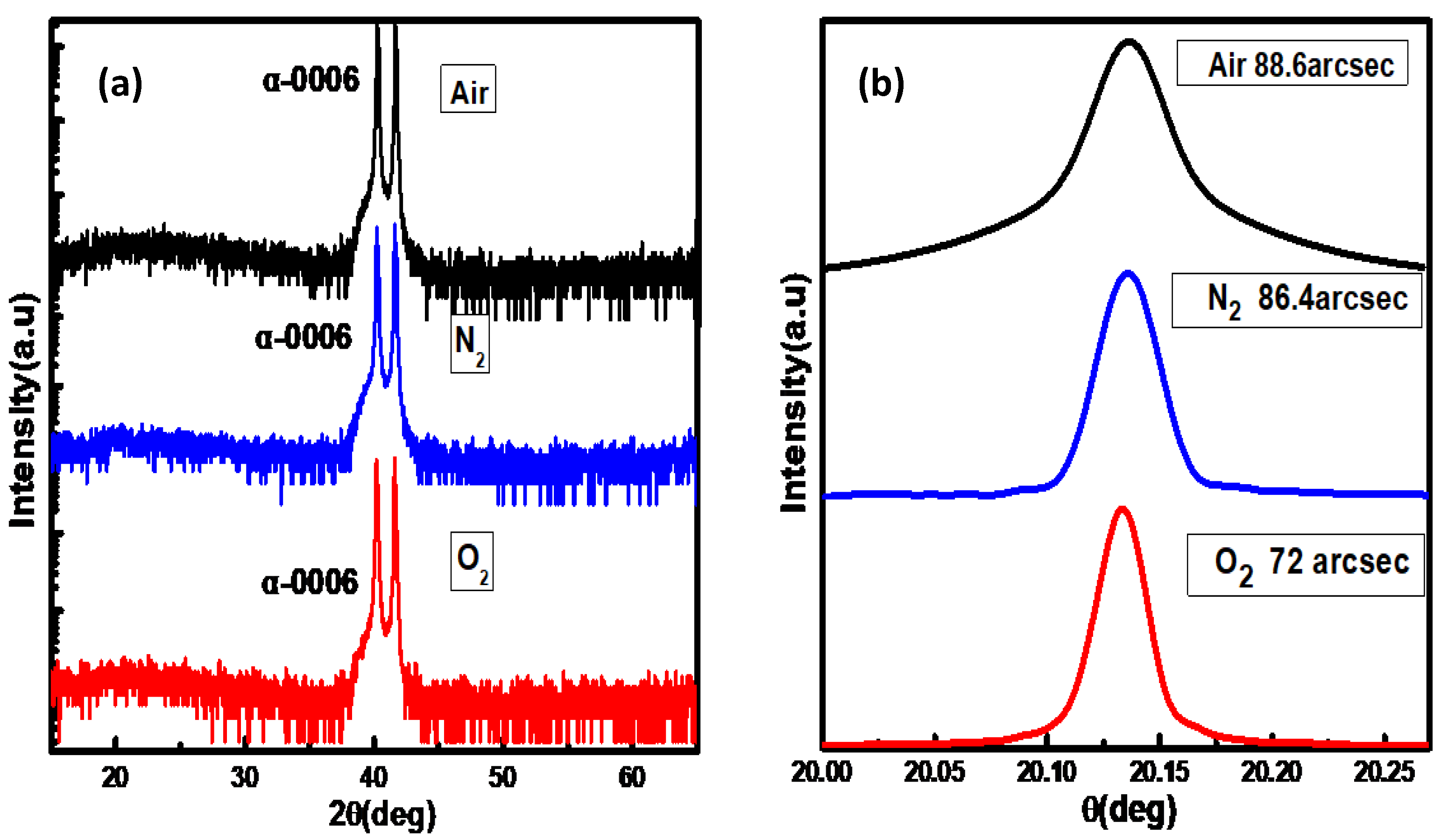
Figure 1 shows the XRD spectra of the samples with air, N
2, and O
2 as the carrier gases. The spectra are dominated by the diffraction peaks at 40.26° and 41.66°, which correspond to the (0006) planes of α-Ga
2O
3 epilayer and sapphire substrate, respectively. No other peaks are found, which shows that all of the Ga
2O
3 films show the obvious pure alpha phase. These XRD spectra show that the α-Ga
2O
3 films had a preferential c-axis orientation along the c-axis of the sapphire substrate and the calculated lattice constant along the c-axis is 1.34 nm. Paying attention to the sample grown with O
2 as the carrier gas, the full-width at half maximum (FWHM) of the ω scan rocking curve is as small as 72 arcsec, indicating a high quality α-Ga
2O
3. However, for the samples grown with air and N
2 as the carrier gases, FWHM of the ω scan rocking curves are 88.6 arcsec and 86.4 arcsec, respectively, indicating a relatively inferior crystal quality. Considering the different oxygen content in the carrier gases, it is supposed that Ga
2O
3 film grown with O
2 as the carrier gas has less defects, such as oxygen vacancies (V
O), which may be the key to improving the quality of crystallization.
Raman spectra of the epilayers grown with air, N
2, and O
2 as the carrier gases were measured between 100 cm
−1 and 800 cm
−1 at room temperature to confirm the crystalline quality of the deposited films, and the results are presented in
Figure 2. A 514 nm laser was used as the excitation source and the laser beam was focused by a microscope lens system (×50 ulwd) yielding a spot size of 1 μm during the Raman measurement. The Raman peaks at 418 cm
−1 and 749 cm
−1 belong to the sapphire substrate [
14]. The Raman peaks located at 431.3 cm
−1, 577 cm
−1, and 692 cm
−1 are the Raman-allowed vibrational modes of E
g, A
1g, and E
g for α-Ga
2O
3, respectively, and are consistent with the theoretical calculations [
15]. The high-frequency A
1g mode at 577 cm
−1 mainly involves the vibration of oxygen atoms perpendicular to the c-axis. The linewidth of the peak A
1g is as narrow as 3.9 cm
−1 for the epilayer grown with O
2 as the carrier gas, strongly suggesting the high crystallinity of the epilayer. By comparing the epilayers grown with different carrier gases, the displacement and intensity of the Raman peaks do not change obviously, demonstrating that the stress in the films is mainly determined by other factors, such as lattice mismatch or growth temperature, instead of the carrier gases. It could also be observed that except the Raman peaks of α-Ga
2O
3, no other peaks are observed in the Raman spectra, which indicates that all of the epilayers are pure α-Ga
2O
3 without other phases and confirm the conclusion from the XRD measurements.
The variation of optical transmittance spectra (200–800 nm) were performed on α-Ga
2O
3 films as shown in
Figure 3. All the samples exhibited a transmittance higher than 80% in the visible to near-UV regions. The relationship between the absorption coefficient α and the optical bandgap (E
g) is αhν = A(hν−Eg)
1/2, where A is the material-dependent constant, h is the Planck’s constant, and ν is the frequency of the incident light [
16]. The optical band gap can be evaluated from the (αhν)
2 versus photon energy (hν) graph by linear extrapolations to zero absorption coefficient [
17]. The inset shows the plot of (αhν)
2 as function of photon-energy hν. The bandgaps of the obtained materials remained at 5.1–5.3 eV, which is obviously larger than that of β-Ga
2O
3. The larger bandgap than that of β-Ga
2O
3 is obviously attributed to the crystal structure of α-Ga
2O
3 being different from β-Ga
2O
3. We note that the α-Ga
2O
3 sample grown with O
2 as the carrier gas is dropped more abruptly than those of air and N
2 in ultraviolet region. This phenomenon may be caused by less defect in α-Ga
2O
3 samples carried by O
2. During the film growth, extra oxygen will ensure the ideal ratio of O to Ga atomic, which results in higher crystalline quality and leads to its bandgap being close to the ideal value of 5.3 eV. The higher crystalline quality for the sample with O
2 as the carrier gas is consistent with the XRD measurement results.
Figure 4a shows the electron diffraction patterns of the Ga
2O
3/Al
2O
3 interface for the sample with O
2 as the carrier gas. The diffraction patterns of both the Ga
2O
3 film and the Al
2O
3 substrate are rectangular, corresponding to the corundum-structure. All of the diffraction spots of α-Ga
2O
3 are situated almost in the α-Al
2O
3 spots. The cross-sectional HR-TEM image at the α-Ga
2O
3/α-Al
2O
3 interface is shown in
Figure 4b. As a result of the in-plane strain, the α-Ga
2O
3/α-Al
2O
3 interface is unclearly identified. At the α-Ga
2O
3/α-Al
2O
3 interface, we can observe a dark area and this is induced by the in-plane compressive strain in the α-Ga
2O
3 layer because the lattice constant of α-Ga
2O
3 is larger than that of α-Al
2O
3 substrate. The TEM images for the samples, with air and N
2 as the carrier gases in
Figures S1 and S2 also demonstrate the similar electron diffraction patterns and obvious HR-TEM lattice structures, indicating that all of the samples achieve a pure α-Ga
2O
3 phase and confirm the conclusion from the XRD measurements again. By comparing the HR-TEM images for the three different samples, the samples with O
2 and air as the carrier gases show a more complete lattice structure than the sample with N
2 as the carrier gas, which shows that the adequate efficient oxygen content is essential for the high quality film growth and this result is the same with that from the XRD measurement. The α-Ga
2O
3 films deposited on sapphire substrates obtain the thicknesses of 619 nm, 318 nm, and 146 nm for the samples with O
2, air, and N
2 as the carrier gases, respectively. These thicknesses correspond to the different growth rates of 10.3 nm/min, 5.3 nm/min, and 2.4 nm/min as shown in
Figure 4c. Variable-angle Spectral Ellipsometry (SE) measurements were performed at room temperature in ambient atmosphere with an electronically controlled rotating compensator and Glan Taylor polarizers (J. A. Woollam Co., Lincoln, NE, USA). The Cauchy model was used to fit the thickness of Ga
2O
3 thin film. Measurements were carried out at three different incidence angles of 55°, 65°, and 75° over the 193–1000 nm wavelength range. Considering the different oxygen contents in the carrier gases, it can be concluded that more oxygen in the carrier gas can promote the growth rate greatly, and at the same time it can also guarantee the crystal quality as demonstrated by the XRD, UV-VIS and TEM measurements.
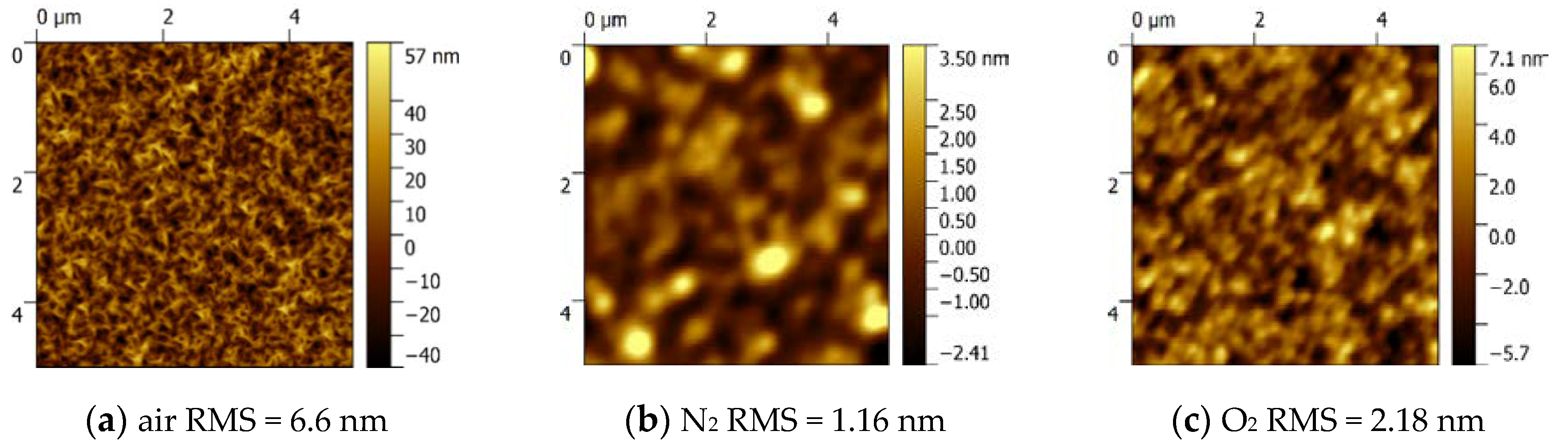
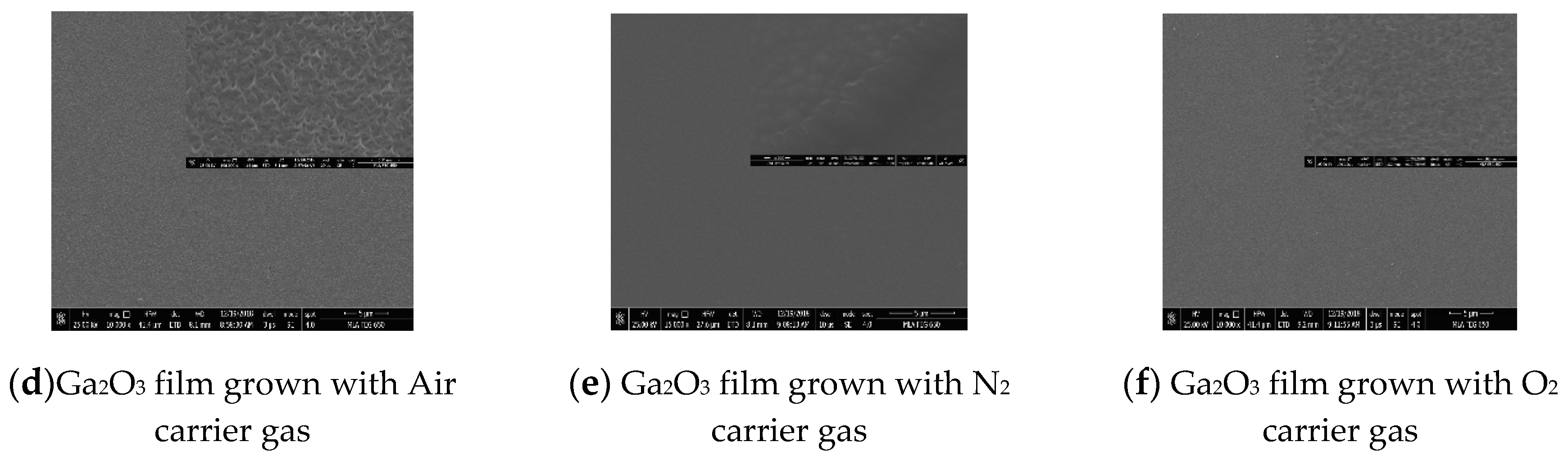
Figure 5 shows the AFM images for the α-Ga
2O
3 films prepared by different carrier gases of air (a), N
2 (b), and O
2(c). The films have root-mean-square (RMS) surface roughness values of 6.6 nm, 1.16 nm and 2.18 nm, respectively, measured over an area of 5 × 5 μm
2. The surface morphology for the sample grown with air as the carrier gas is rough and composed of irregular stripes, while the surface morphologies of α-Ga
2O
3 thin films grown with N
2 and O
2 as the carrier gases are much smoother. It is inferred that the complex components in air induced this rough surface, and the reason behind that requires more research in the future. On the contrary, the pure carrier gas will lead to a much smoother surface. Comparing the sample grown with O
2 as the carrier gas to the sample with N
2 as the carrier gas, although the growth rate is improved by about five times, the difference between their RMS values is relatively small. This means that the rapid growth rate with O
2 as the carrier gas will not degrade the surface morphology. To further investigate the microstructure, we measured SEM images of all α-Ga
2O
3 films as shown in
Figure 5d–f. As demonstrated in the enlarged pictures, it can be seen that the film grown with air as the carrier gas has indeed a rough surface, and the other samples show the relatively smooth surface, which confirm the results from the AFM measurement.
To assess the elemental composition of the α-Ga
2O
3 films, XPS measurements were conducted for the epitaxial films on sapphire. The result for the sample with O
2 as the carrier gas is presented in
Figure 6a and only three elements (C, Ga, and O) are observed in the films. The position of the Ga 2
p3/2 and Ga 3
d binding energy peaks confirms the presence of Ga
2O
3 [
18]. It can be observed from the spectra that the Ga2
p3/2 and Ga2
p1/2 signal peaks are located at 1118.5 eV and 1145.5 eV respectively, The energy difference between the two signal peaks is about 27 eV, which is consistent with the Ga2
p signal peak energy difference reported in the literature [
19]. The binding energy position of Ga3
d signal is 21.05 eV, which is consistent with the results reported in the literature [
20]. The result for the samples with air as the carrier gases is shown in
Figures S3 and S4. The same peak positions appear in both samples and no significant peak shift and peak intensity changes are observed, indicating the same pure α-Ga
2O
3 and correspond to the XRD and Raman results.
Figure 6b–d show the peaks of O 1
s signal around 530.6 eV for the three samples. O 1s signal peaks do not show Gaussian symmetry so Gaussian fitting was carried out for the peaks. It is found that the strong O 1
s signal peaks appear at 530.6 eV and 532.1 eV. The peak at 530.6 eV originated from the oxygen element in Ga–O bond, while the peak at 532.1 eV originated from the adsorption O on the sample surface [
21].
Figure 5e–f show Ga 3
d spectra. The chemical compositions of the surfaces were determined from the area of the Ga 3
d, O 1
s, and C 1
s peaks taking into account the corresponding sensitivity factors [
22]. The calculated atomic ratios of O to Ga for the samples grown with air, N
2, and O
2 as the carrier gases were 1.53, 1.51, and 1.56, respectively. It reveals that more oxygen present in the carrier gas can slightly increase the O content of the film, which confirms the guess in the XRD measurement.
We also compared the quality of the same thickness and growth rate of the α-Ga
2O
3 films grown by different carrier gases. As shown in
Figure S2 in the supplemental information, the growth rate of the α-Ga
2O
3 films was set to 10 nm/min for all samples. In
Figure S3 in the supplemental information, the thicknesses of all α-Ga
2O
3 samples were 500 nm. The optical transmittance spectra show that when O
2 is the carrier gas, the absorption edge is closer to 234 nm of α-Ga
2O
3 and the downward trend of the absorption edge is more obvious. From the AFM images, we assume that with the same growth rate and film thickness, the complex components in air induces rough surface and the pure carrier gas will lead to a much smoother surface. These results fully demonstrate that the partial pressure of oxygen in the carrier gas component can improve the quality of the film, consistent with the above results.


 ,
, 


