A Theoretical Treatment of THz Resonances in Semiconductor GaAs p–n Junctions


Abstract
1. Introduction
2. Material Properties
3. Dispersion Relation for the p–n Junction of an Inhomogeneous Dielectric Constant
4. Results
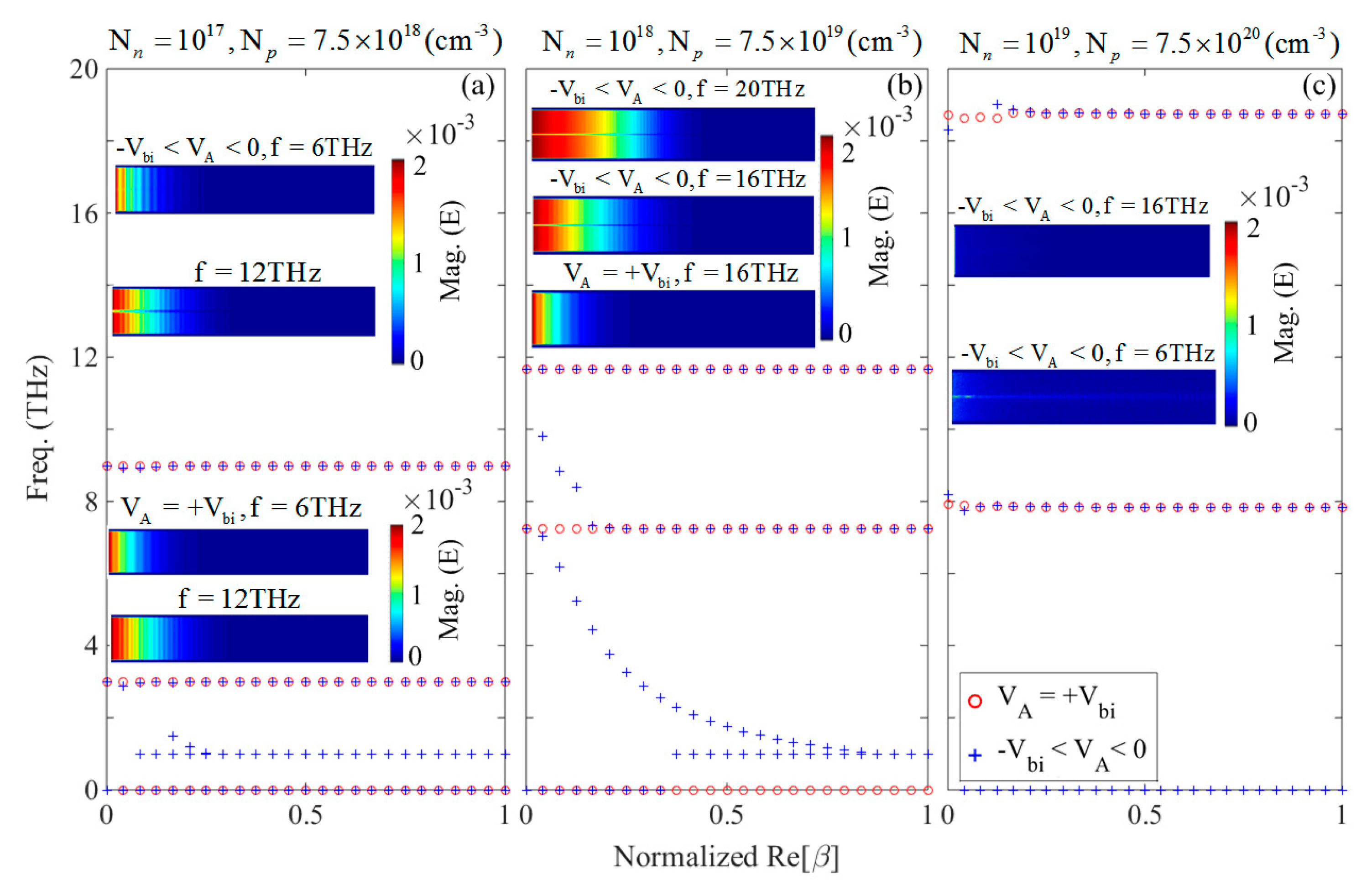
4.1. Symmetric Doping Densities
4.2. Asymmetric Doping Densities
5. Conclusions
Author Contributions
Funding
Conflicts of Interest
References
- Yariv, A.; Leite, R.C.C. Dielectric-waveguide mode of light propagation in p–n junctions. Appl. Phys. Lett. 1963, 2, 55–57. [Google Scholar] [CrossRef]
- Bond, W.L.; Cohen, B.G.; Leite, R.C.C.; Yariv, A. Observation of the dielectric-waveguide mode of light propagation in p–n junctions. Appl. Phys. Lett. 1963, 2, 57–59. [Google Scholar] [CrossRef]
- Wei, H.; Zhang, S.; Tian, X.; Xu, H. Highly tunable propagating surface plasmons on supported silver nanowires. Proc. Natl. Acad. Sci. USA 2013, 110, 4494–4499. [Google Scholar] [CrossRef] [PubMed]
- Zhang, S.; Wei, H.; Bao, K.; Håkanson, U.; Halas, N.J.; Nordlander, P.; Xu, H. Chiral surface plasmon polaritons on metallic nanowires. Phys. Rev. Lett. 2011, 107, 096801. [Google Scholar] [CrossRef] [PubMed]
- Holmgaard, T.; Chen, Z.; Bozhevolnyi, S.I.; Markey, L.; Dereux, A.; Krasavin, A.V.; Zayats, A.V. Wavelength selection by dielectric-loaded plasmonic components. Appl. Phys. Lett. 2009, 94, 051111. [Google Scholar] [CrossRef]
- Chen, Z.; Holmgaard, T.; Bozhevolnyi, S.I.; Krasavin, A.V.; Zayats, A.V.; Markey, L.; Dereux, A. Wavelength-selective directional coupling with dielectric-loaded plasmonic waveguides. Opt. Lett. 2009, 34, 310. [Google Scholar] [CrossRef]
- Bian, Y.; Gong, Q. Tuning the hybridization of plasmonic and coupled dielectric nanowire modes for high-performance optical waveguiding at sub-diffraction-limited scale. Sci. Rep. 2014, 4, 6617. [Google Scholar] [CrossRef]
- Holmgaard, T.; Chen, Z.; Bozhevolnyi, S.I.; Markey, L.; Dereux, A.; Krasavin, A.V.; Zayats, A.V. Bend- and splitting loss of dielectric-loaded surface plasmon-polariton waveguides. Opt. Express 2008, 16, 13585. [Google Scholar] [CrossRef]
- Burke, J.J.; Stegeman, G.I.; Tamir, T. Surface-polariton-like waves guided by thin, lossy metal films. Phys. Rev. B 1986, 33, 5186–5201. [Google Scholar] [CrossRef]
- Dionne, J.A.; Sweatlock, L.A.; Atwater, H.A.; Polman, A. Plasmon slot waveguides: Towards chip-scale propagation with subwavelength-scale localization. Phys. Rev. B 2006, 73, 035407. [Google Scholar] [CrossRef]
- Maier, S.A. Plasmonics: Fundamentals and Applications; Springer: New York, NY, USA, 2007. [Google Scholar]
- Fedyanin, D.Y.; Yakubovsky, D.I.; Kirtaev, R.V.; Volkov, V.S. Ultralow-loss CMOS copper plasmonic waveguides. Nano Lett. 2016, 16, 362–366. [Google Scholar] [CrossRef]
- Krasavin, A.V.; Zayats, A.V. Silicon-based plasmonic waveguides. Opt. Express 2010, 18, 11791. [Google Scholar] [CrossRef]
- Zektzer, R.; Desiatov, B.; Mazurski, N.; Bozhevolnyi, S.I.; Levy, U. Experimental demonstration of CMOS-compatible long-range dielectric-loaded surface plasmon-polariton waveguides (LR-DLSPPWs). Opt. Express 2014, 22, 22009. [Google Scholar] [CrossRef]
- Lotan, O.; Smith, C.L.C.; Bar-David, J.; Mortensen, N.A.; Kristensen, A.; Levy, U. Propagation of channel plasmons at the visible regime in aluminum v-groove waveguides. ACS Photonics 2016, 3, 2150–2157. [Google Scholar] [CrossRef]
- Larson, L.E.; Hackett, R.H.; Lohr, R.F. Microactuators for GaAs-Based microwave integrated circuits. In Proceedings of the International Conference Solid-State Sensors and Actuators, San Francisco, CA, USA, 24–27 June 1991. [Google Scholar]
- Yeh, H.-J.J.; Smith, J.S. Fluidic self-assembly for the integration of GaAs light-emitting diodes on Si substrates. IEEE Photonics Technol. Lett. 1994, 6, 706–708. [Google Scholar] [CrossRef]
- Dupuis, R.D.; Dapkus, P.D.; Holonyak, N.; Rezek, E.A.; Chin, R. Room-temperature laser operation of quantum-well Ga(1−x)AlxAs-GaAs laser diodes grown by metalorganic chemical vapor deposition. Appl. Phys. Lett. 1978, 32, 295–297. [Google Scholar] [CrossRef]
- Yablonovitch, E.; Miller, O.D.; Kurtz, S.R. The opto-electronic physics that broke the efficiency limit in solar cells. In Proceedings of the 38th IEEE Conference Photovoltaic Specialists, Austin, TX, USA, 3–8 June 2012. [Google Scholar]
- Pitilakis, A.; Kriezis, E.E. Highly nonlinear hybrid silicon-plasmonic waveguides: Analysis and optimization. J. Opt. Soc. Am. B 2013, 30, 1954. [Google Scholar] [CrossRef]
- Chou, L.-W.; Shin, N.; Sivaram, S.V.; Filler, M.A. Tunable mid-infrared localized surface plasmon resonances in silicon nanowires. J. Am. Chem. Soc. 2012, 134, 16155–16158. [Google Scholar] [CrossRef]
- Law, S.; Podolskiy, V.; Wasserman, D. Towards nano-scale photonics with micro-scale photons: The opportunities and challenges of mid-infrared plasmonics. Nanophotonics 2013, 2, 103–130. [Google Scholar] [CrossRef]
- Kinsey, N.; Ferrera, M.; Shalaev, V.M.; Boltasseva, A. Examining nanophotonics for integrated hybrid systems: A review of plasmonic interconnects and modulators using traditional and alternative materials [Invited]. J. Opt. Soc. Am. B 2015, 32, 121. [Google Scholar] [CrossRef]
- Janipour, M.; Misirlioglu, I.B.; Sendur, K. Tunable surface plasmon and phonon polariton interactions for moderately doped semiconductor surfaces. Sci. Rep. 2016, 6, 34071. [Google Scholar] [CrossRef]
- Qi, Z.; Hu, G.; Li, L.; Yun, B.; Zhang, R.; Cui, Y. Design and analysis of a compact SOI-based aluminum/highly doped p-type silicon hybrid plasmonic modulator. IEEE Photonics J. 2016, 8, 1–11. [Google Scholar] [CrossRef]
- Rodríguez-Fortuño, F.J.; Espinosa-Soria, A.; Martínez, A. Exploiting metamaterials, plasmonics and nanoantennas concepts in silicon photonics. J. Opt. 2016, 18, 123001. [Google Scholar] [CrossRef]
- Law, S.; Adams, D.C.; Taylor, A.M.; Wasserman, D. Mid-infrared designer metals. Opt. Express 2012, 20, 12155. [Google Scholar] [CrossRef]
- Law, S.; Roberts, C.; Kilpatrick, T.; Yu, L.; Ribaudo, T.; Shaner, E.A.; Podolskiy, V.; Wasserman, D. All-semiconductor negative-index plasmonic absorbers. Phys. Rev. Lett. 2014, 112, 017401. [Google Scholar] [CrossRef]
- N’Tsame Guilengui, V.; Cerutti, L.; Rodriguez, J.-B.; Tournié, E.; Taliercio, T. Localized surface plasmon resonances in highly doped semiconductors nanostructures. Appl. Phys. Lett. 2012, 101, 161113. [Google Scholar] [CrossRef]
- Jun, Y.C.; Brener, I. Electrically tunable infrared metamaterials based on depletion-type semiconductor devices. J. Opt. 2012, 14, 114013. [Google Scholar] [CrossRef]
- Luther, J.M.; Jain, P.K.; Ewers, T.; Alivisatos, A.P. Localized surface plasmon resonances arising from free carriers in doped quantum dots. Nat. Mater. 2011, 10, 361–366. [Google Scholar] [CrossRef]
- Williams, C.R.; Andrews, S.R.; Maier, S.A.; Fernández-Domínguez, A.I.; Martín-Moreno, L.; García-Vidal, F.J. Highly confined guiding of terahertz surface plasmon polaritons on structured metal surfaces. Nat. Photonics 2008, 2, 175–179. [Google Scholar] [CrossRef]
- Goykhman, I.; Desiatov, B.; Khurgin, J.; Shappir, J.; Levy, U. Locally oxidized silicon surface-plasmon schottky detector for telecom regime. Nano Lett. 2011, 11, 2219–2224. [Google Scholar] [CrossRef]
- Fedyanin, D.Y.; Arsenin, A.V. Surface plasmon polariton amplification in metal-semiconductor structures. Opt. Express 2011, 19, 12524. [Google Scholar] [CrossRef]
- Fedyanin, D.Y.; Arsenin, A.V.; Chigrin, D.N. Semiconductor surface plasmon amplifier based on a schottky barrier diode. In Proceedings of the AIP Conference Proceedings, Bad Honnef, Germany, 3–5 November 2010; Volume 1291, pp. 112–114. [Google Scholar]
- Li, D.; Ning, C.Z. All-semiconductor active plasmonic system in mid-infrared wavelengths. Opt. Express 2011, 19, 14594. [Google Scholar] [CrossRef] [PubMed]
- Soref, R.; Hendrickson, J.; Cleary, J.W. Mid- to long-wavelength infrared plasmonic-photonics using heavily doped n-Ge/Ge and n-GeSn/GeSn heterostructures. Opt. Express 2012, 20, 3814–3824. [Google Scholar] [CrossRef] [PubMed]
- Fan, P.; Colombo, C.; Huang, K.C.Y.; Krogstrup, P.; Nygård, J.; Fontcuberta i Morral, A.; Brongersma, M.L. An electrically-driven GaAs nanowire surface plasmon source. Nano Lett. 2012, 12, 4943–4947. [Google Scholar] [CrossRef] [PubMed]
- Vinnakota, R.K.; Genov, D.A. Terahertz optoelectronics with surface plasmon polariton diode. Sci. Rep. 2014, 4, 20–27. [Google Scholar]
- Sze, S.M.; Ng, K.K. Physics of Semiconductor Devices, 3rd ed.; Wiley-Interscience: Hoboken, NJ, USA, 2006. [Google Scholar]
- Varga, B.B. Coupling of plasmons to polar phonons in degenerate semiconductors. Phys. Rev. 1965, 137, A1896. [Google Scholar] [CrossRef]
- Mooradian, A.; Wright, G.B. Observation of the interaction of plasmons with longitudinal optical phonons in GaAs. Phys. Rev. Lett. 1966, 16, 999–1001. [Google Scholar] [CrossRef]
- Hase, M.; Nakashima, S.; Mizoguchi, K.; Harima, H.; Sakai, K. Ultrafast decay of coherent plasmon-phonon coupled modes in highly doped GaAs. Phys. Rev. B 1999, 60, 16526–16530. [Google Scholar] [CrossRef]
- Olson, C.G.; Lynch, D.W. Longitudinal-optical-phonon-plasmon coupling in GaAs. Phys. Rev. 1969, 177, 1231–1234. [Google Scholar] [CrossRef]
- Kuznetsov, A.V.; Stanton, C.J. Coherent phonon oscillations in GaAs. Phys. Rev. B 1995, 51, 7555–7565. [Google Scholar] [CrossRef]
- Hu, Z.G.; Rinzan, M.B.M.; Matsik, S.G.; Perera, A.G.U.; Von Winckel, G.; Stintz, A.; Krishna, S. Optical characterizations of heavily doped p-type AlxGa1−xAs and GaAs epitaxial films at terahertz frequencies. J. Appl. Phys. 2005, 97, 093529. [Google Scholar] [CrossRef]
- Fehrenbacher, M.; Winnerl, S.; Schneider, H.; Döring, J.; Kehr, S.C.; Eng, L.M.; Huo, Y.; Schmidt, O.G.; Yao, K.; Liu, Y.; et al. Plasmonic superlensing in doped GaAs. Nano Lett. 2015, 15, 1057–1061. [Google Scholar] [CrossRef]
- Sotoodeh, M.; Khalid, A.H.; Rezazadeh, A.A. Empirical low-field mobility model for III–V compounds applicable in device simulation codes. J. Appl. Phys. 2000, 87, 2890. [Google Scholar] [CrossRef]
- Abernathy, C.R.; Pearton, S.J.; Caruso, R.; Ren, F.; Kovalchik, J. Ultrahigh doping of GaAs by carbon during metalorganic molecular beam epitaxy. Appl. Phys. Lett. 1989, 55, 1750. [Google Scholar] [CrossRef]
- Levi, A.F.J. Scaling ‘ballistic’ heterojunction bipolar transistors. Electron. Lett. 1988, 24, 1273–1275. [Google Scholar] [CrossRef]
- Collin, R.E. Foundations for Microwave Engineering, 2nd ed.; Wiley: Hoboken, NJ, USA, 2000. [Google Scholar]
- Pierret, R.F. Semiconductor Device Fundamentals; Addison Wesley: Boston, MA, USA, 1996. [Google Scholar]
- Cunningham, S.L.; Maradudin, A.A.; Wallis, R.F. Effect of a charge layer on the surface-plasmon-polariton dispersion curve. Phys. Rev. B 1974, 10, 3342–3355. [Google Scholar] [CrossRef]
- Kretschmann, E.; Raether, H. Radiative decay of non radiative surface plasmons excited by light. Z. Naturforsch. A 1968, 23, 2135–2136. [Google Scholar] [CrossRef]
- Branch, M.A.; Coleman, T.F.; Li, Y. A Subspace, Interior, and conjugate gradient method for large-scale bound-constrained minimization problems. SIAM J. Sci. Comput. 1999, 21, 1–23. [Google Scholar] [CrossRef]


| 12.9 | 10.9 | 8 | 8.5 | 0.055 |
© 2019 by the authors. Licensee MDPI, Basel, Switzerland. This article is an open access article distributed under the terms and conditions of the Creative Commons Attribution (CC BY) license (http://creativecommons.org/licenses/by/4.0/).
Share and Cite
Janipour, M.; Misirlioglu, I.B.; Sendur, K. A Theoretical Treatment of THz Resonances in Semiconductor GaAs p–n Junctions. Materials 2019, 12, 2412. https://doi.org/10.3390/ma12152412
Janipour M, Misirlioglu IB, Sendur K. A Theoretical Treatment of THz Resonances in Semiconductor GaAs p–n Junctions. Materials. 2019; 12(15):2412. https://doi.org/10.3390/ma12152412
Chicago/Turabian StyleJanipour, Mohsen, I. Burc Misirlioglu, and Kursat Sendur. 2019. "A Theoretical Treatment of THz Resonances in Semiconductor GaAs p–n Junctions" Materials 12, no. 15: 2412. https://doi.org/10.3390/ma12152412
APA StyleJanipour, M., Misirlioglu, I. B., & Sendur, K. (2019). A Theoretical Treatment of THz Resonances in Semiconductor GaAs p–n Junctions. Materials, 12(15), 2412. https://doi.org/10.3390/ma12152412