Hybrid Top-Down/Bottom-Up Fabrication of a Highly Uniform and Organized Faceted AlN Nanorod Scaffold

 , ,
, ,  and
and 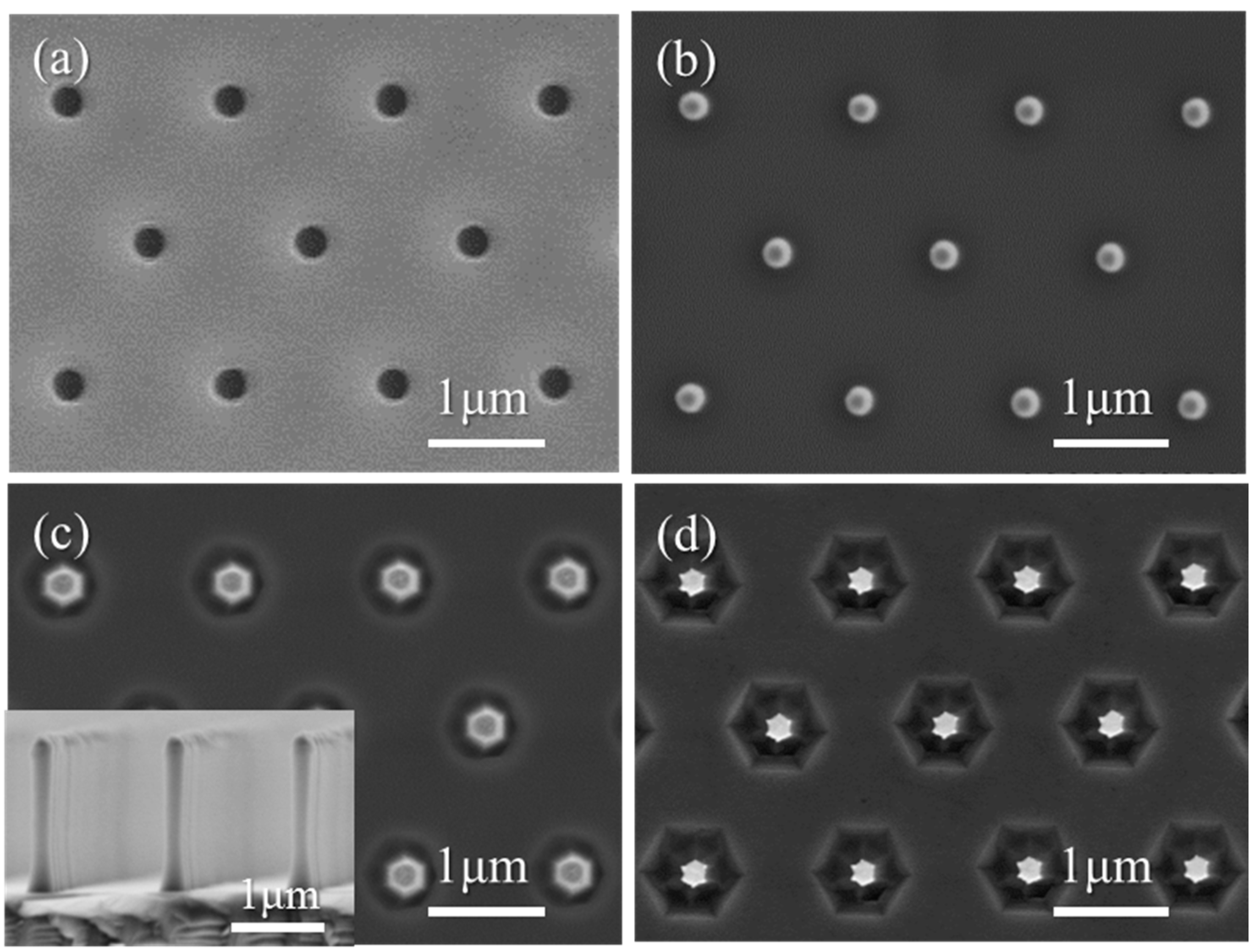
Abstract
1. Introduction
2. Materials and Methods
3. Results and Discussion
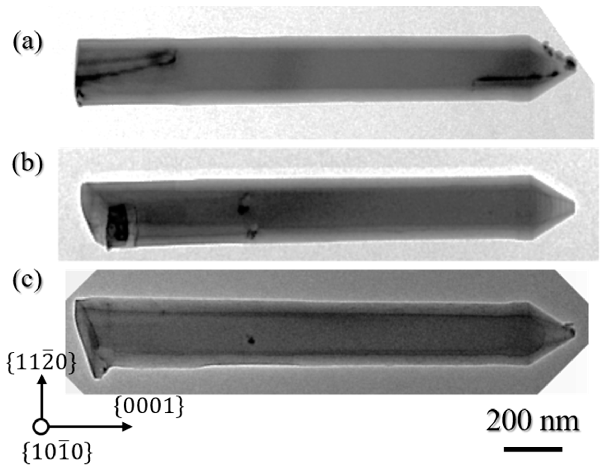
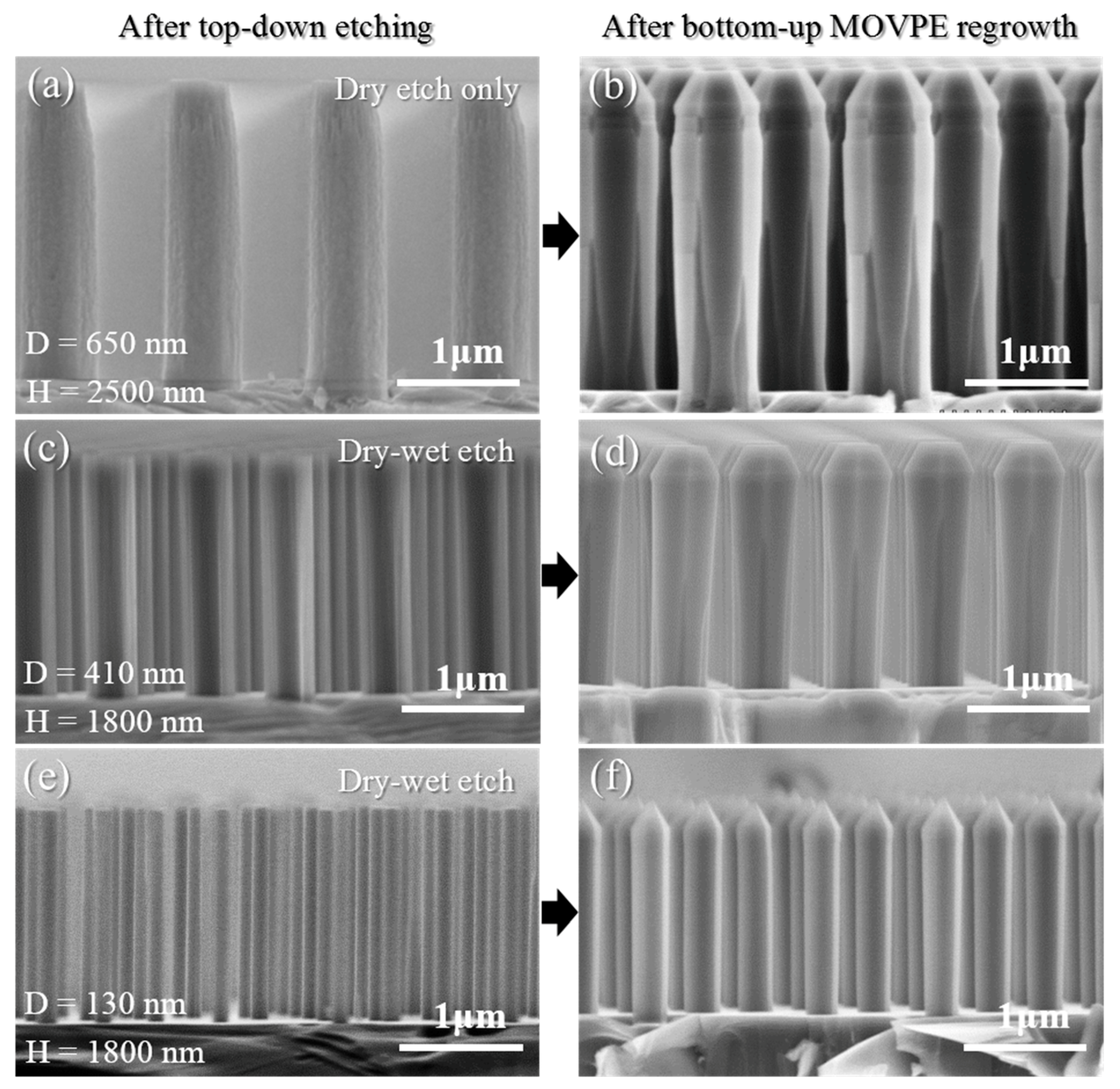
3.1. Morphology and Structural Quality of Top-Down Etched AlN Nanorods
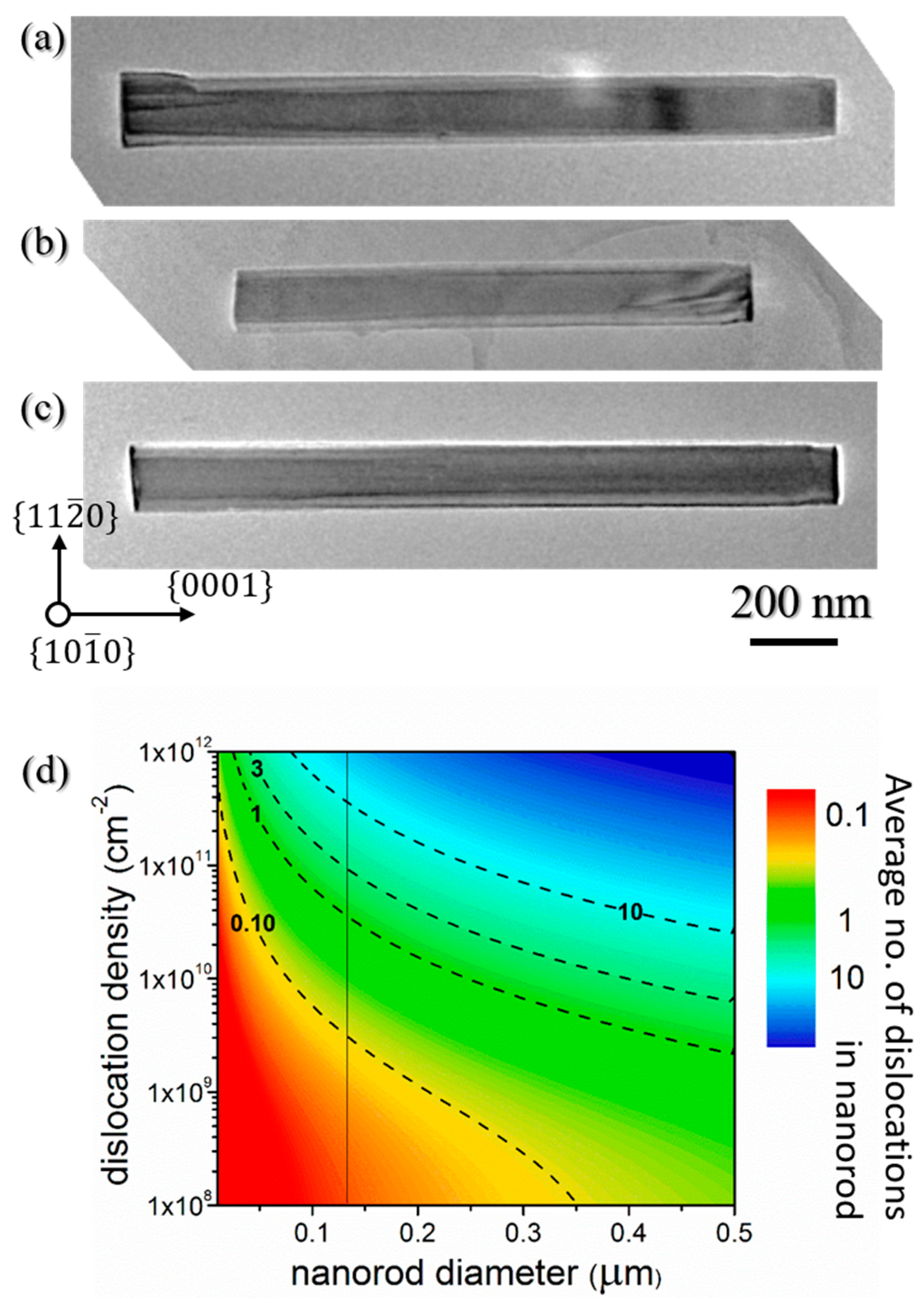
3.2. Morphology and Structural Quality of Bottom-Up Regrown AlN Nanorod
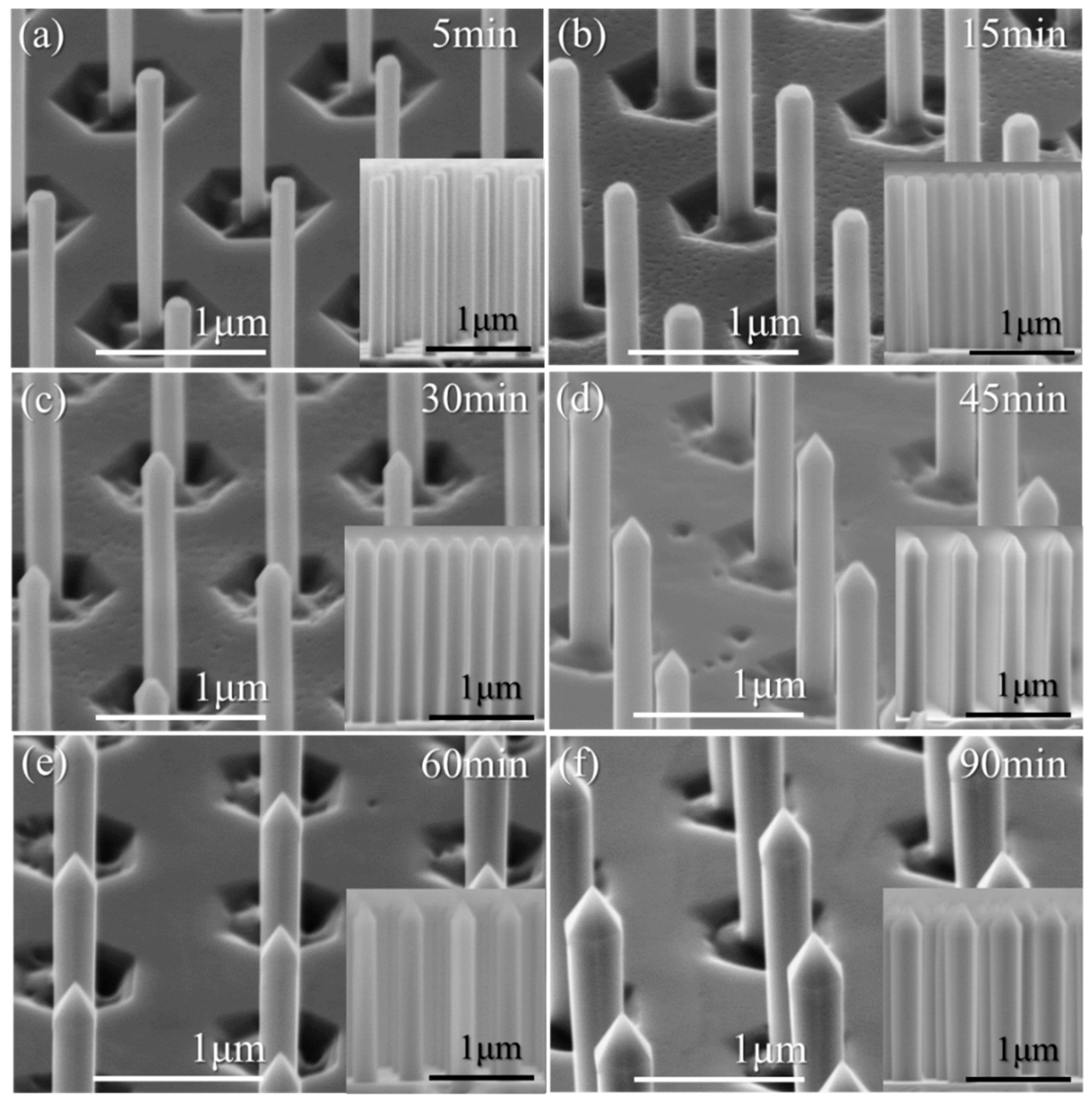
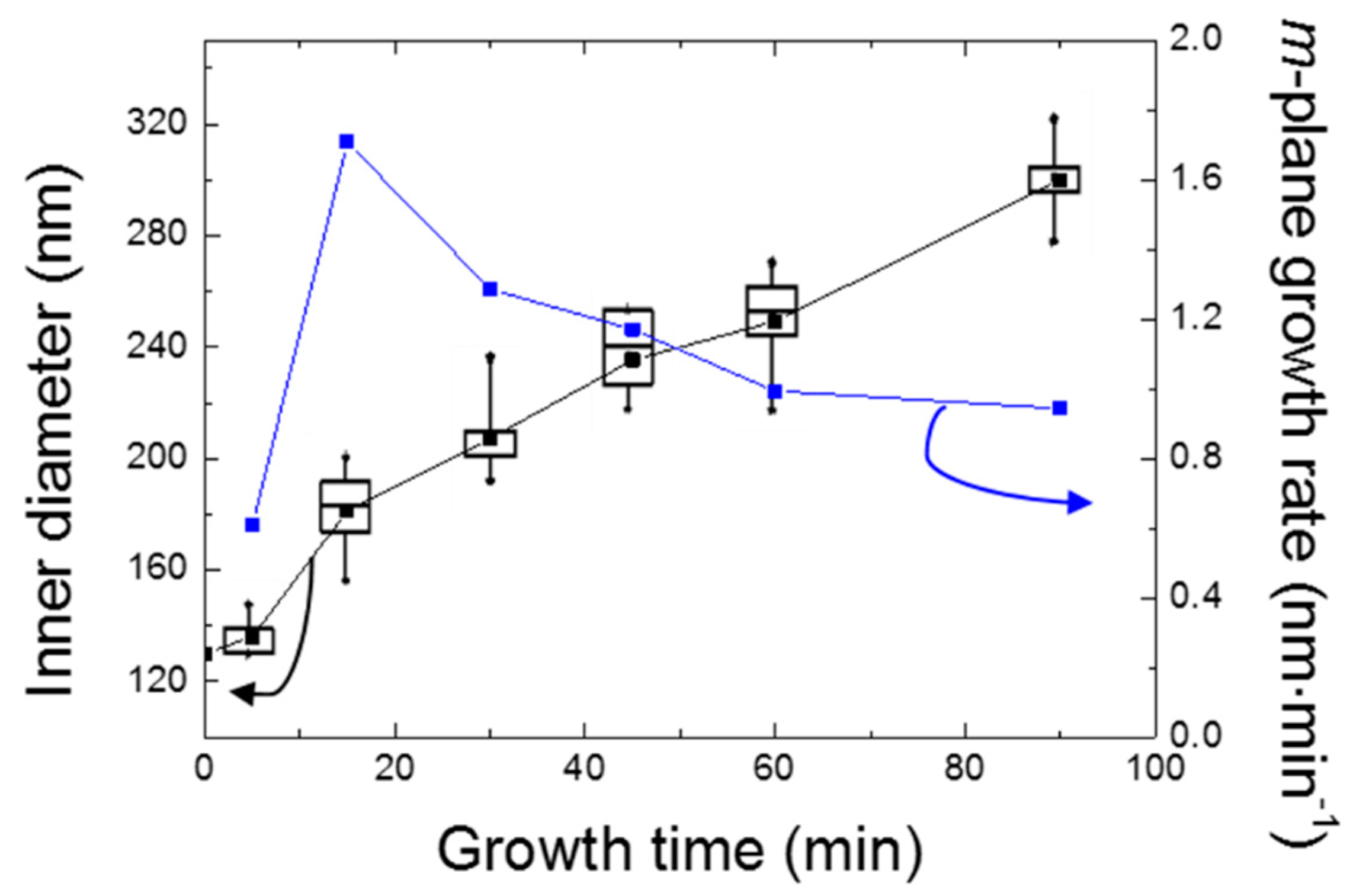
3.3. Impact of the Etched Nanorod Morphology and Dimensions on the AlN Faceting
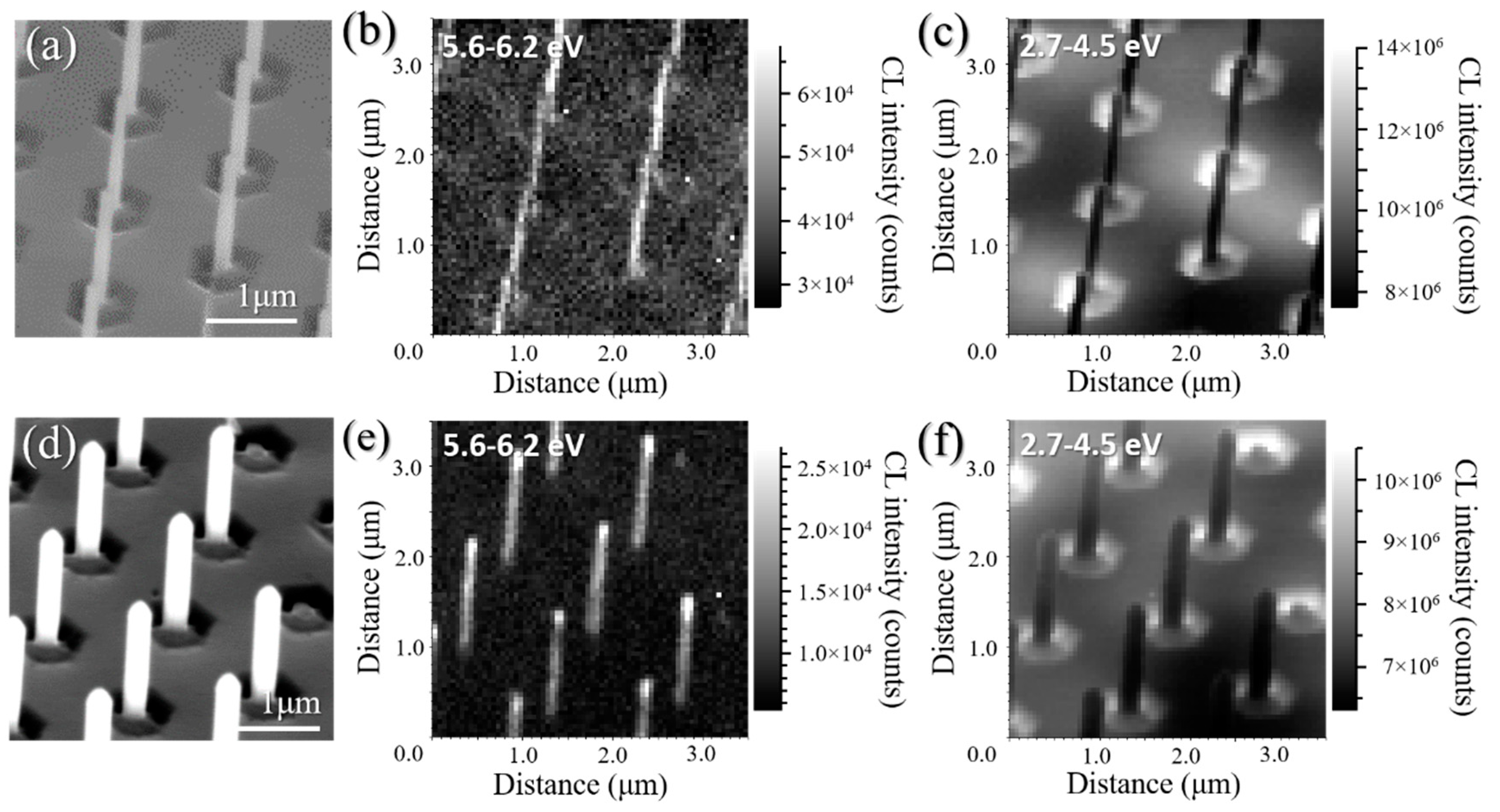
3.4. Optical Properties
4. Conclusions
Supplementary Materials
Author Contributions
Funding
Conflicts of Interest
References
- Anayaogu, K.C.; Ermoshkin, A.A.; Neckers, D.C.; Mejiritski, A.; Grinevich, O.; Fedorov, A.V. Performance of the light emitting diodes versus conventional light sources in the UV light cured formulations. J. Appl. Polym. Sci. 2007, 105, 803–808. [Google Scholar] [CrossRef]
- Morison, W.L. Phototherapy and Photochemotherapy of Skin Disease, 2nd ed.; Raven Press: New York, NY, USA, 1991. [Google Scholar]
- Hodgkinson, J.; Tatam, R.P. Optical gas sensing: A review. Meas. Sci. Technol. 2013, 24, 012004. [Google Scholar] [CrossRef]
- Wu, T.; Zha, Q.; Chen, W.; Xu, Z.; Wang, T.; He, X. Development and deployment of a cavity enhanced UV-LED spectrometer for measurements of atmospheric HONO and NO2 in Hong Kong. Atmos. Environ. 2014, 95, 544–551. [Google Scholar] [CrossRef]
- Xu, Z.; Sadler, B.M. Ultraviolet communications: Potential and state-of-the-art. IEEE Commun. Mag. 2008, 46, 67–73. [Google Scholar]
- Vilhunen, S.; Särkkä, H.; Sillanpää, M. Ultraviolet light-emitting diodes in water disinfection. Environ. Sci. Pollut. Res. 2009, 16, 439–442. [Google Scholar] [CrossRef] [PubMed]
- Würtele, M.A.; Kolbe, T.; Lipsz, M.; Külberg, A.; Weyers, M.; Kneissl, M.; Jekel, M. Application of GaN-based deep ultraviolet light emitting diodes UV-LEDs for Water disinfection. Water Res. 2011, 45, 1481–1489. [Google Scholar] [CrossRef] [PubMed]
- Kneissl, M.; Rass, J. III-Nitride Ultraviolet Emitters; Springer Series in Materials Science; Springer International Publishing: Cham, Switzerland, 2016; Volume 227. [Google Scholar]
- Zyara, A.M.; Heinonen-Tanski, H.; Veijalainen, A.-M.; Torvinen, E. UV-LEDs Efficiently Inactivate DNA and RNA Coliphages. Water 2017, 9, 46. [Google Scholar] [CrossRef]
- Hirayama, H.; Maeda, N.; Fujikawa, S.; Toyoda, S.; Kamata, N. Recent progress and future prospects of AlGaN-based high-efficiency deep-ultraviolet light-emitting diodes. Jpn. J. Appl. Phys. 2014, 53, 100209. [Google Scholar] [CrossRef]
- Kneissl, M.; Kolbe, T.; Chua, C.; Kueller, V.; Lobo, N.; Stellmach, J.; Knauer, A.; Rodriguez, H.; Einfeldt, S.; Yang, Z.; et al. Advances in group III-nitride-based deep UV light-emitting diode technology. Semicond. Sci. Technol. 2011, 26, 014036. [Google Scholar] [CrossRef]
- Martens, M.; Mehnke, F.; Kuhn, C.; Reich, C.; Kueller, V.; Knauer, A.; Netzel, C.; Hartmann, C.; Wollweber, J.; Rass, J.; et al. Performance Characteristics of UV-C AlGaN-Based Lasers Grown on Sapphire and Bulk AlN Substrates. IEEE Photonics Technol. Lett. 2014, 26, 342–345. [Google Scholar] [CrossRef]
- Amano, H.; Miyazaki, A.; Iida, K.; Kawashima, T.; Iwaya, M.; Kamiyama, S.; Akasaki, I.; Liu, R.; Bell, A.; Ponce, F.A.; et al. Defect and stress control of AlGaN for fabrication of high performance UV light emitters. Phys. Status Solidi 2004, 201, 2679–2685. [Google Scholar] [CrossRef]
- Ban, K.; Yamamoto, J.; Takeda, K.; Ide, K.; Iwaya, M.; Takeuchi, T.; Kamiyama, S.; Akasaki, I.; Amano, H. Internal Quantum Efficiency of Whole-Composition-Range AlGaN Multiquantum Wells. Appl. Phys. Express 2011, 4, 052101. [Google Scholar] [CrossRef]
- Stampfl, C.; Neugebauer, J.; Van De Walle, C.G. Doping of AlxGa1−xN alloys. Mater. Sci. Eng. B 1999, 59, 253–257. [Google Scholar] [CrossRef]
- Khan, M.A.; Shatalov, M.; Maruska, H.P.; Wang, H.M.; Kuokstis, E. III-Nitride UV Devices. Jpn. J. Appl. Phys. 2005, 44, 7191. [Google Scholar] [CrossRef]
- Huang, M.-F.; Lu, T.-H. Optimization of the Active-Layer Structure for the Deep-UV AlGaN Light-Emitting Diodes. IEEE J. Quantum Electron. 2006, 42, 820–826. [Google Scholar] [CrossRef]
- Shur, M.S.; Gaska, R. Deep-Ultraviolet Light-Emitting Diodes. IEEE Trans. Electron. Devices 2010, 57, 12–25. [Google Scholar] [CrossRef]
- Nam, K.B.; Li, J.; Nakarmi, M.L.; Lin, J.Y.; Jiang, H.X. Unique optical properties of AlGaN alloys and related ultraviolet emitters. Appl. Phys. Lett. 2004, 84, 5264–5266. [Google Scholar] [CrossRef]
- Taniyasu, Y.; Kasu, M. Surface 210 nm light emission from an AlN p–n junction light-emitting diode enhanced by A-plane growth orientation. Appl. Phys. Lett. 2010, 96, 221110. [Google Scholar] [CrossRef]
- Kim, D.; Park, J.H.; Lee, J.W.; Hwang, S.; Oh, S.J.; Kim, J.; Sone, C.; Schubert, E.F.; Kim, J.K. Overcoming the fundamental light-extraction efficiency limitations of deep ultraviolet light-emitting diodes by utilizing transverse-magnetic-dominant emission. Light Sci. Appl. 2015, 4, e263. [Google Scholar] [CrossRef]
- Park, J.-S.; Kim, J.K.; Cho, J.; Seonga, T.-Y. Review—Group III-Nitride-Based Ultraviolet Light-Emitting Diodes: Ways of Increasing External Quantum Efficiency. ECS J. Solid State Sci. Technol. 2017, 6, Q42–Q52. [Google Scholar] [CrossRef]
- Coulon, P.-M.; Mexis, M.; Teisseire, M.; Jublot, M.; Vennéguès, P.; Leroux, M.; Zúñiga-Pérez, J. Double-polarity GaN micropillars grown by metalorganic vapour phase epitaxy: Cross correlation between structural and optical properties. J. Appl. Phys. 2014, 115, 153504. [Google Scholar] [CrossRef]
- Coulon, P.-M.; Alloing, B.; Brändli, V.; Vennéguès, P.; Leroux, M.; Zúñiga-Pérez, J. Dislocation-filtering and polarity in the selective area growth of GaN nanowires by continuous-flow MOVPE. Appl. Phys. Express 2016, 9, 015502. [Google Scholar] [CrossRef]
- Wang, G.T.; Li, Q.; Wierer, J.J.; Koleske, D.D.; Figiel, J.J. Top-down fabrication and characterization of axial and radial III-nitride nanowire LEDs. Phys. Status Solidi 2014, 211, 748–751. [Google Scholar] [CrossRef]
- Waag, A.; Wang, X.; Fündling, S.; Ledig, J.; Erenburg, M.; Neumann, R.; Al Suleiman, M.; Merzsch, S.; Wei, J.; Li, S.; et al. The nanorod approach: GaN NanoLEDs for solid state lighting. Phys. Status Solidi 2011, 8, 2296–2301. [Google Scholar] [CrossRef]
- Li, S.; Waag, A. GaN based nanorods for solid state lighting. J. Appl. Phys. 2012, 111, 071101. [Google Scholar] [CrossRef]
- Ryu, H.Y.; Choi, I.G.; Choi, H.S.; Shim, J.I. Investigation of Light Extraction Efficiency in AlGaN Deep-Ultraviolet Light-Emitting Diodes. Appl. Phys. Express 2013, 6, 062101. [Google Scholar] [CrossRef]
- Lee, D.; Lee, J.W.; Jang, J.; Shin, I.-S.; Jin, L.; Park, J.H.; Kim, J.; Lee, J.; Noh, H.-S.; Kim, Y.-I.; et al. Improved performance of AlGaN-based deep ultraviolet light-emitting diodes with nano-patterned AlN/sapphire substrates. Appl. Phys. Lett. 2017, 110, 191103. [Google Scholar] [CrossRef]
- Inoue, S.-I.; Tamari, N.; Taniguchi, M. 150 mW deep-ultraviolet light-emitting diodes with large-area AlN nanophotonic lightextraction structure emitting at 265 nm. Appl. Phys. Lett. 2017, 110, 141106. [Google Scholar] [CrossRef]
- Bergbauer, W.; Strassburg, M.; Kölper, C.; Linder, N.; Roder, C.; Lähnemann, J.; Trampert, A.; Fündling, S.; Li, S.F.; Wehmann, H.H.; et al. Continuous-flux MOVPE growth of position-controlled N-face GaN nanorods and embedded InGaN quantum wells. Nanotechnology 2010, 21, 305201. [Google Scholar] [CrossRef] [PubMed]
- Choi, K.; Arita, M.; Arakawa, Y. Selective-area growth of thin GaN nanowires by MOCVD. J. Cryst. Growth 2012, 357, 58–61. [Google Scholar] [CrossRef]
- Coulon, P.-M.; Alloing, B.; Brändli, V.; Lefebvre, D.; Chenot, S.; Zúñiga-Pérez, J. Selective area growth of Ga-polar GaN nanowire arrays by continuous-flow MOVPE: A systematic study on the effect of growth conditions on the array properties. Phys. Status Solidi 2015, 252, 1096–1103. [Google Scholar] [CrossRef]
- Su, J.; Gherasimova, M.; Cui, G.; Tsukamoto, H.; Han, J.; Onuma, T.; Kurimoto, M.; Chichibu, S.F.; Broadbridge, C.; He, Y.; et al. Growth of AlGaN nanowires by metalorganic chemical vapor deposition. Appl. Phys. Lett. 2005, 87, 183108. [Google Scholar] [CrossRef]
- Zheng, J.; Yang, Y.; Yu, B.; Song, X.B.; Li, X.G. [0001] Oriented Aluminum Nitride One-Dimensional Nanostructures: Synthesis, Structure Evolution, and Electrical Properties. ACS Nano 2008, 2, 134–142. [Google Scholar] [CrossRef] [PubMed]
- Yeh, T.-W.; Lin, Y.-T.; Stewart, L.S.; Dapkus, P.D.; Sarkissian, R.; O’Brien, J.D.; Ahn, B.; Nutt, S.R. InGaN/GaN Multiple Quantum Wells Grown on Nonpolar Facets of Vertical GaN Nanorod Arrays. Nano Lett. 2012, 12, 3257–3262. [Google Scholar] [CrossRef] [PubMed]
- Jung, B.O.; Bae, S.; Lee, S.; Kim, S.Y.; Lee, J.Y.; Honda, Y.; Amano, H. Emission Characteristics of InGaN/GaN Core-Shell Nanorods Embedded in a 3D Light-Emitting Diode. Nanoscale Res. Lett. 2016, 11, 215. [Google Scholar] [CrossRef] [PubMed]
- Banal, R.G.; Funato, M.; Kawakami, Y. Surface diffusion during metalorganic vapor phase epitaxy of AlN. Phys. Status Solidi 2009, 6, 599–602. [Google Scholar] [CrossRef]
- Zhao, S.; Liu, X.; Woo, S.Y.; Kang, J.; Botton, G.A.; Mi, Z. An electrically injected AlGaN nanowire laser operating in the ultraviolet-C band. Appl. Phys. Lett. 2015, 107, 043101. [Google Scholar] [CrossRef]
- Zhao, S.; Liu, X.; Wu, Y.; Mi, Z. An electrically pumped 239 nm AlGaN nanowire laser operating at room temperature. Appl. Phys. Lett. 2016, 109, 191106. [Google Scholar] [CrossRef]
- Sadaf, S.M.; Zhao, S.; Wu, Y.; Ra, Y.H.; Liu, X.; Vanka, S.; Mi, Z. An AlGaN Core−Shell Tunnel Junction Nanowire Light-Emitting Diode Operating in the Ultraviolet C Band. Nano Lett. 2017, 17, 1212–1218. [Google Scholar] [CrossRef] [PubMed]
- Belloeil, M.; Gayral, B.; Daudin, B. Quantum Dot-Like Behavior of Compositional Fluctuations in AlGaN Nanowires. Nano Lett. 2016, 16, 960–966. [Google Scholar] [CrossRef] [PubMed]
- Bengoechea-Encabo, A.; Albert, A.; Müller, M.; Xie, M.-Y.; Veit, P.; Bertram, F.; Sanchez-Garcia, M.A.; Zúñiga-Pérez, J.; Mierry, P.D.; Christen, J.; et al. Selective Area Growth of AlN/GaN Nanocolumns on (0001) and (11–22) GaN/Sapphire for SemiPolar and Non-Polar AlN Pseudo-Templates. Nanotechnology 2017, 28, 365704. [Google Scholar] [CrossRef] [PubMed]
- Le Boulbar, E.D.; Gîrgel, I.; Lewins, C.J.; Edwards, P.R.; Martin, R.W.; Šatka, A.; Allsopp, D.W.E.; Shields, P.A. Facet recovery and light emission from GaN/InGaN/GaN core-shell structures grown by metal organic vapour phase epitaxy on etched GaN nanorod arrays. J. Appl. Phys. 2013, 114, 094302. [Google Scholar] [CrossRef]
- Le Boulbar, E.D.; Edwards, P.R.; Vajargah, S.H.; Griffiths, I.; Gîrgel, I.; Coulon, P.-M.; Cherns, D.; Martin, R.W.; Humphreys, C.J.; Bowen, C.R.; et al. Structural and Optical Emission Uniformity of m-Plane InGaN Single Quantum Wells in Core–Shell Nanorods. Cryst. Growth Des. 2016, 16, 1907–1916. [Google Scholar] [CrossRef]
- Li, C.; Wright, J.B.; Liu, S.; Lu, P.; Figiel, J.J.; Leung, B.; Chow, W.W.; Brener, I.; Koleske, D.D.; Luk, T.S.; et al. Nonpolar InGaN/GaN Core–Shell Single Nanowire Lasers. Nano Lett. 2017, 17, 1049–1055. [Google Scholar] [CrossRef] [PubMed]
- Tian, Y.; Yan, J.; Zhang, Y.; Zhang, Y.; Chen, X.; Guo, Y.; Wang, J.; Li, J. Formation and characteristics of AlGaN-based three-dimensional hexagonal nanopyramid semi-polar multiple quantum wells. Nanoscale 2016, 8, 11012–11018. [Google Scholar] [CrossRef] [PubMed]
- Coulon, P.-M.; Kusch, G.; Le Boulbar, E.D.; Chausse, P.; Bryce, C.; Martin, R.W.; Shields, P.A. Hybrid Top-Down/Bottom-Up Fabrication of Regular Arrays of AlN Nanorods for Deep-UV Core-Shell LEDs. Phys. Status Solidi 2017, 6, 599–602. [Google Scholar] [CrossRef]
- Edwards, P.R.; Jagadamma, L.K.; Bruckbauer, J.; Liu, C.; Shields, P.; Allsopp, D.; Wang, T.; Martin, R.W. High-Resolution Cathodoluminescence Hyperspectral Imaging of Nitride Nanostructures. Microscopy Microanal. 2012, 18, 1212–1219. [Google Scholar] [CrossRef] [PubMed]
- Li, Q.; Wright, J.B.; Chow, W.W.; Luk, T.S.; Brener, I.; Lester, L.F.; Wang, G.T. Single-Mode GaN Nanowire Lasers. Opt. Express 2012, 20, 17873–17879. [Google Scholar] [CrossRef] [PubMed]
- Bryan, Z.; Bryan, I.; Bobea, M.; Hussey, L.; Kirste, R.; Sitar, Z.; Collazo, R. Homoepitaxial AlN thin films deposited on m-plane (1¯100) AlN substrates by metalorganic chemical vapor deposition. J. Appl. Phys. 2014, 115, 133503. [Google Scholar] [CrossRef]
- Dadgar, A.; Krost, A.; Christen, J.; Bastek, B.; Bertram, F.; Krtschil, A.; Hempel, T.; Bläsing, J.; Haboeck, U.; Hoffmann, A. MOVPE growth of high-quality AlN. J. Cryst. Growth 2006, 297, 306–310. [Google Scholar] [CrossRef]


© 2018 by the authors. Licensee MDPI, Basel, Switzerland. This article is an open access article distributed under the terms and conditions of the Creative Commons Attribution (CC BY) license (http://creativecommons.org/licenses/by/4.0/).
Share and Cite
Coulon, P.-M.; Kusch, G.; Fletcher, P.; Chausse, P.; Martin, R.W.; Shields, P.A. Hybrid Top-Down/Bottom-Up Fabrication of a Highly Uniform and Organized Faceted AlN Nanorod Scaffold. Materials 2018, 11, 1140. https://doi.org/10.3390/ma11071140
Coulon P-M, Kusch G, Fletcher P, Chausse P, Martin RW, Shields PA. Hybrid Top-Down/Bottom-Up Fabrication of a Highly Uniform and Organized Faceted AlN Nanorod Scaffold. Materials. 2018; 11(7):1140. https://doi.org/10.3390/ma11071140
Chicago/Turabian StyleCoulon, Pierre-Marie, Gunnar Kusch, Philip Fletcher, Pierre Chausse, Robert W. Martin, and Philip A. Shields. 2018. "Hybrid Top-Down/Bottom-Up Fabrication of a Highly Uniform and Organized Faceted AlN Nanorod Scaffold" Materials 11, no. 7: 1140. https://doi.org/10.3390/ma11071140
APA StyleCoulon, P.-M., Kusch, G., Fletcher, P., Chausse, P., Martin, R. W., & Shields, P. A. (2018). Hybrid Top-Down/Bottom-Up Fabrication of a Highly Uniform and Organized Faceted AlN Nanorod Scaffold. Materials, 11(7), 1140. https://doi.org/10.3390/ma11071140