Characterisation of InGaN by Photoconductive Atomic Force Microscopy


Abstract
1. Introduction
2. Results
2.1. Samples
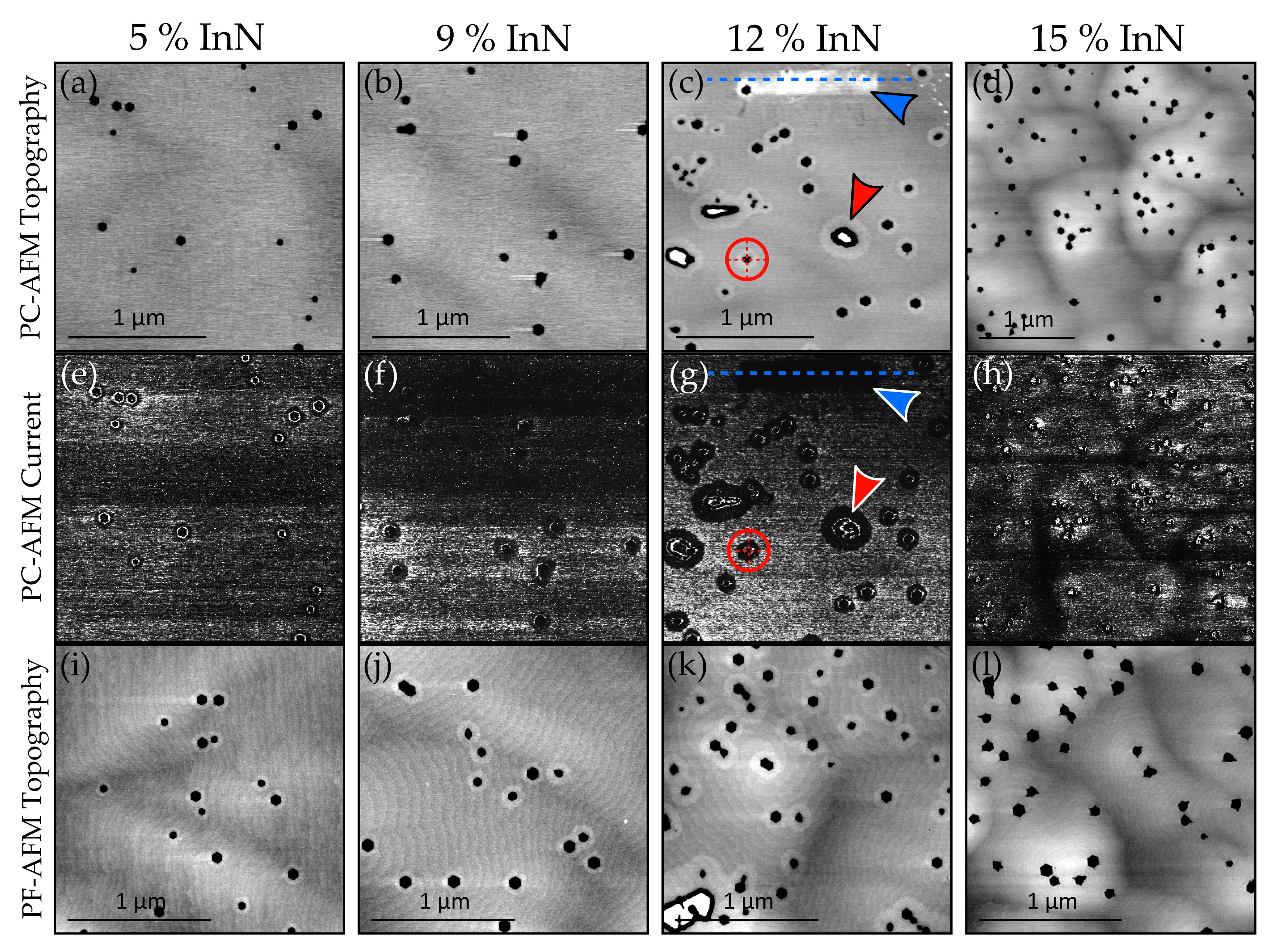
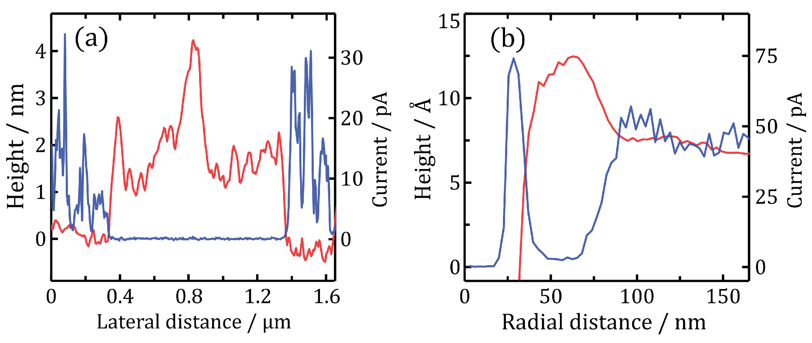
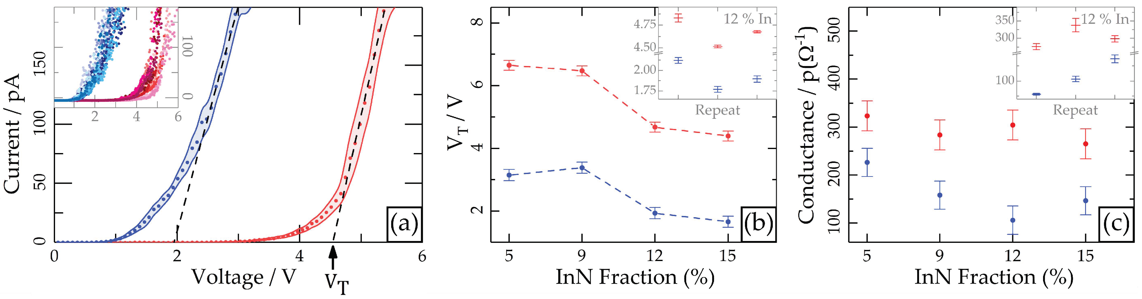
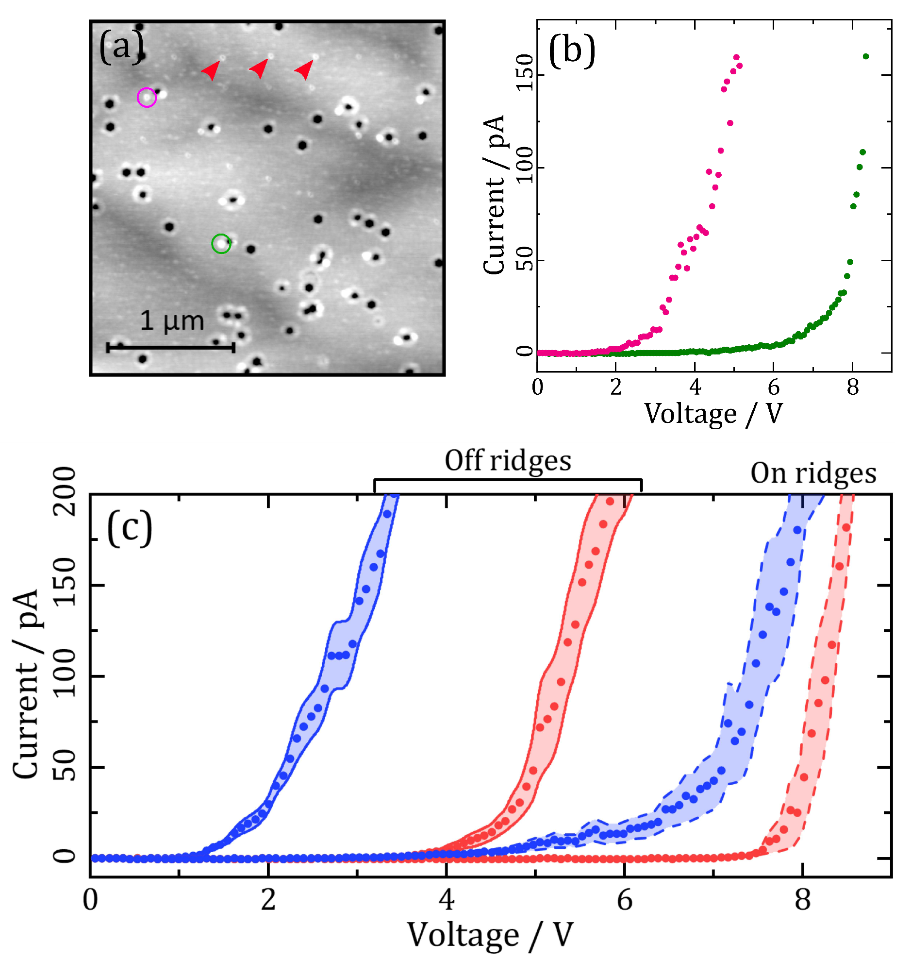
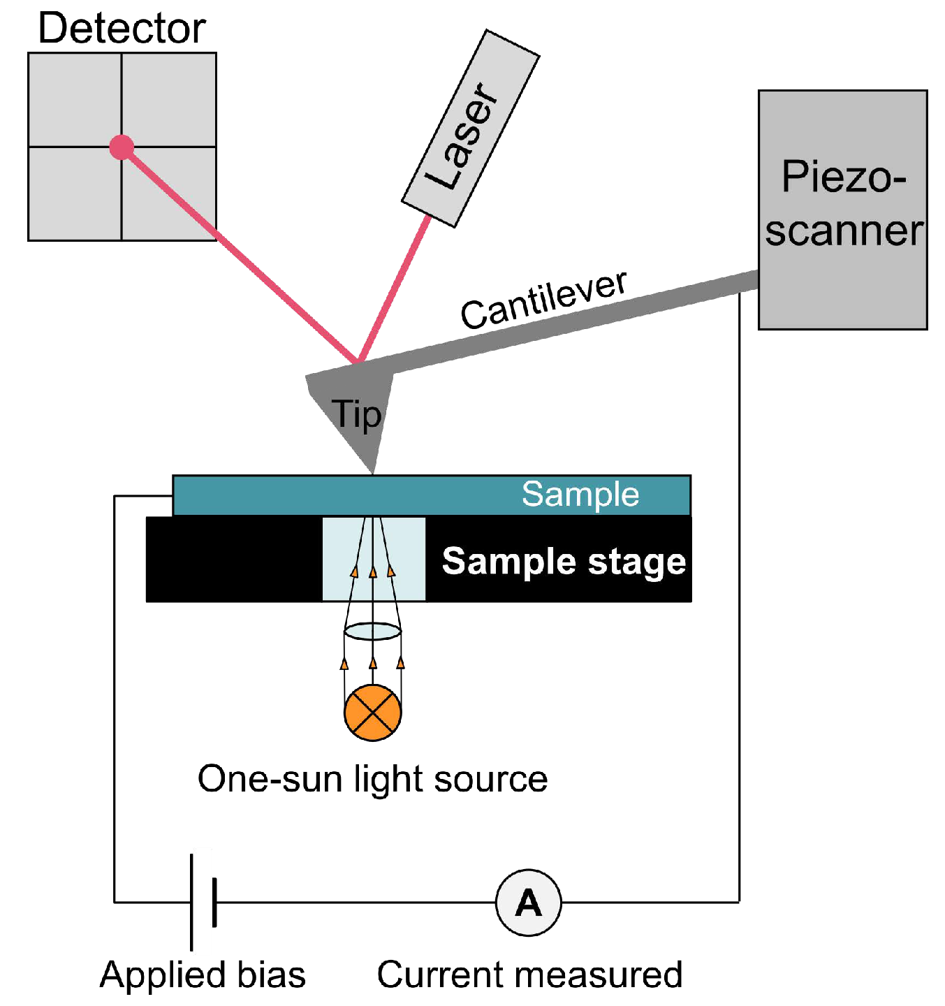
2.2. PC-AFM
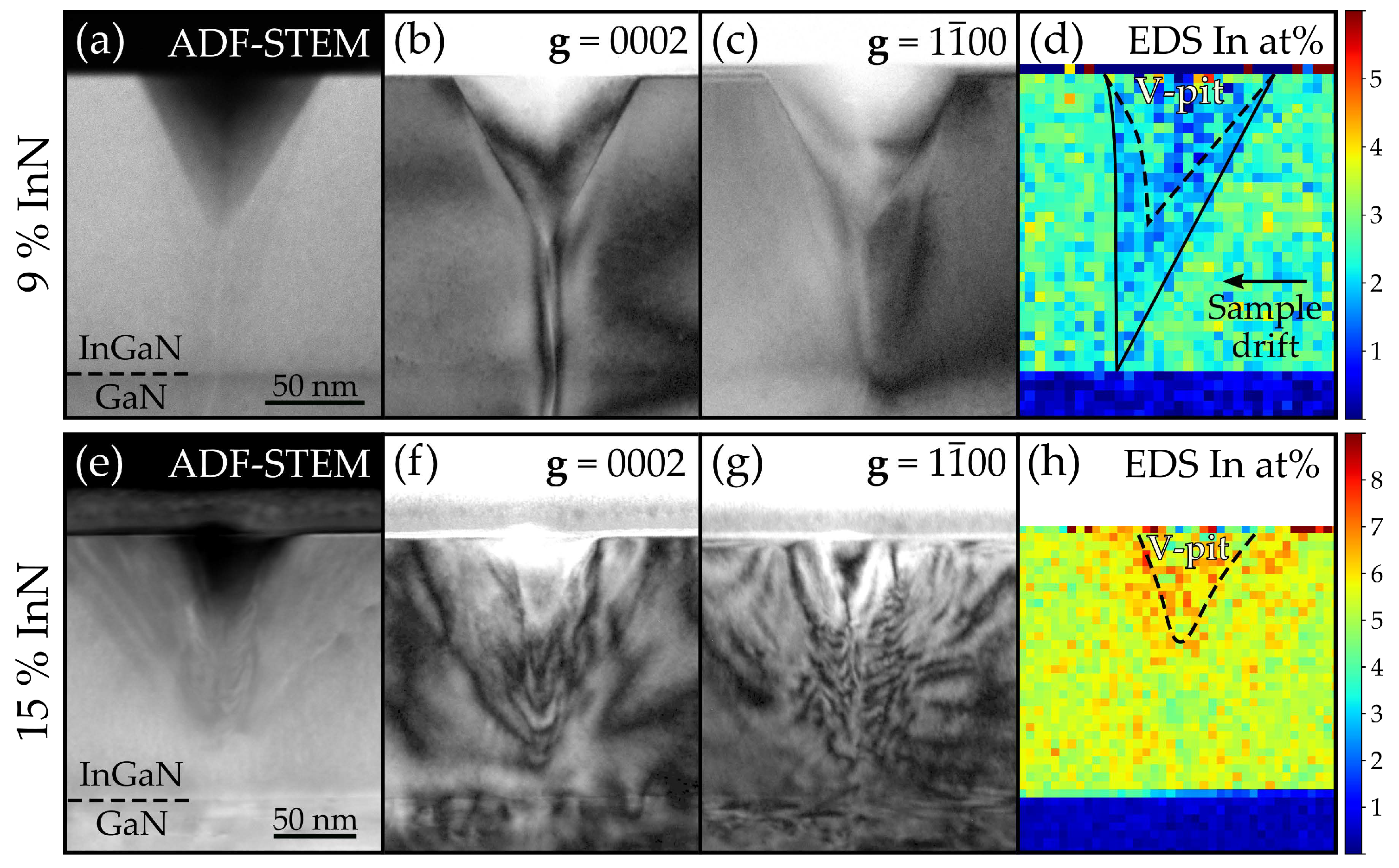
2.3. TEM
3. Discussion
4. Materials and Methods
5. Conclusions
Author Contributions
Funding
Conflicts of Interest
References
- Vurgaftman, I.; Meyer, J.R. Band parameters for nitrogen-containing semiconductors. J. Appl. Phys. 2003, 94, 3675–3696. [Google Scholar] [CrossRef]
- Schubert, E.F. Light-Emitting Diodes; Cambridge University Press: Cambridge, UK, 2006. [Google Scholar]
- Humphreys, C.J. Solid-State Lighting. MRS Bull. 2008, 33, 459–471. [Google Scholar] [CrossRef]
- Dwiliński, R.; Doradziński, R.; Garczyński, J.; Sierzputowski, L.P.; Puchalski, A.; Kanbara, Y.; Yagi, K.; Minakuchi, H.; Hayashi, H. Excellent crystallinity of truly bulk ammonothermal GaN. J. Cryst. Growth 2008, 310, 3911–3916. [Google Scholar] [CrossRef]
- Kukushkin, S.A.; Osipov, A.V.; Bessolov, V.N.; Medvedev, B.K.; Nevolin, V.K.; Tcarik, K.A. Substrates for epitaxy of gallium nitride: New materials and techniques. Rev. Adv. Mater. Sci. 2008, 17, 1–32. [Google Scholar]
- Oliver, R.A. Critical assessment 23: Gallium nitride-based visible light-emitting diodes. Mater. Sci. Technol. 2016, 32, 737–745. [Google Scholar] [CrossRef]
- Massabuau, F.C.P.; Chen, P.; Horton, M.K.; Rhode, S.L.; Ren, C.X.; O’Hanlon, T.J.; Kovács, A.; Kappers, M.J.; Humphreys, C.J.; Dunin-Borkowski, R.E.; et al. Carrier localization in the vicinity of dislocations in InGaN. J. Appl. Phys. 2017, 121, 013104. [Google Scholar] [CrossRef]
- Hsu, J.W.P.; Manfra, M.J.; Chu, S.N.G.; Chen, C.H.; Pfeiffer, L.N.; Molnar, R.J. Effect of growth stoichiometry on the electrical activity of screw dislocations in GaN films grown by molecular-beam epitaxy. Appl. Phys. Lett. 2001, 78, 3980–3982. [Google Scholar] [CrossRef]
- Hsu, J.W.P.; Manfra, M.J.; Molnar, R.J.; Heying, B.; Speck, J.S. Direct imaging of reverse-bias leakage through pure screw dislocations in GaN films grown by molecular beam epitaxy on GaN templates. Appl. Phys. Lett. 2002, 81, 79–81. [Google Scholar] [CrossRef]
- Simpkins, B.S.; Schaadt, D.M.; Yu, E.T.; Molnar, R.J. Scanning Kelvin probe microscopy of surface electronic structure in GaN grown by hydride vapor phase epitaxy. J. Appl. Phys. 2002, 91, 9924–9929. [Google Scholar] [CrossRef]
- Simpkins, B.S.; Yu, E.T.; Waltereit, P.; Speck, J.S. Correlated scanning Kelvin probe and conductive atomic force microscopy studies of dislocations in gallium nitride. J. Appl. Phys. 2003, 94, 1448–1453. [Google Scholar] [CrossRef]
- Moore, J.C.; Ortiz, J.E.; Xie, J.; Morkoç, H.; Baski, A.A. Study of leakage defects on GaN films by conductive atomic force microscopy. J. Phys. Conf. Ser. 2007, 61, 90–94. [Google Scholar] [CrossRef]
- Law, J.J.M.; Yu, E.T.; Koblmüller, G.; Wu, F.; Speck, J.S. Low defect-mediated reverse-bias leakage in (0001) GaN via high-temperature molecular beam epitaxy. Appl. Phys. Lett. 2010, 96, 102111. [Google Scholar] [CrossRef]
- Hofer, A.; Benstetter, G.; Biberger, R.; Leirer, C.; Brüderl, G. Analysis of crystal defects on GaN-based semiconductors with advanced scanning probe microscope techniques. Thin Solid Films 2013, 544, 139–143. [Google Scholar] [CrossRef]
- Miller, E.J.; Schaadt, D.M.; Yu, E.T.; Poblenz, C.; Elsass, C.; Speck, J.S. Reduction of reverse-bias leakage current in Schottky diodes on GaN grown by molecular-beam epitaxy using surface modification with an atomic force microscope. J. Appl. Phys. 2002, 91, 9821–9826. [Google Scholar] [CrossRef]
- Miller, E.J.; Schaadt, D.M.; Yu, E.T.; Sun, X.L.; Brillson, L.J.; Waltereit, P.; Speck, J.S. Origin and microscopic mechanism for suppression of leakage currents in Schottky contacts to GaN grown by molecular-beam epitaxy. J. Appl. Phys. 2003, 94, 7611–7615. [Google Scholar] [CrossRef]
- Porti, M.; Iglesias, V.; Wu, Q.; Couso, C.; Claramunt, S.; Nafría, M.; Cordes, A.; Bersuker, G. CAFM experimental considerations and measurement methodology for in-line monitoring and quantitative analysis of III-V materials defects. IEEE Trans. Nanotechnol. 2016, 15, 986–992. [Google Scholar] [CrossRef]
- Kim, J.; Tak, Y.; Kim, J.; Chae, S.; Kim, J.K.; Park, Y. Analysis of forward tunneling current in InGaN/GaN multiple quantum well light-emitting diodes grown on Si (111) substrate. J. Appl. Phys. 2013, 114, 13101. [Google Scholar] [CrossRef]
- Wu, X.H.; Elsass, C.R.; Abare, A.; Mack, M.; Keller, S.; Petroff, P.M.; DenBaars, S.P.; Speck, J.S.; Rosner, S.J. Structural origin of V-defects and correlation with localized excitonic centers in InGaN/GaN multiple quantum wells. Appl. Phys. Lett. 1998, 72, 692–694. [Google Scholar] [CrossRef]
- Oliver, R.A. Advances in AFM for the electrical characterization of semiconductors. Rep. Prog. Phys. 2008, 71, 076501. [Google Scholar] [CrossRef]
- O’Dea, J.R.; Brown, L.M.; Hoepker, N.; Marohn, J.A.; Sadewasser, S. Scanning probe microscopy of solar cells: From inorganic thin films to organic photovoltaics. MRS Bull. 2012, 37, 642–650. [Google Scholar] [CrossRef]
- Neufeld, C.J.; Toledo, N.G.; Cruz, S.C.; Iza, M.; DenBaars, S.P.; Mishra, U.K. High quantum efficiency InGaN/GaN solar cells with 2.95 eV band gap. Appl. Phys. Lett. 2008, 93, 143502. [Google Scholar] [CrossRef]
- Hangleiter, A.; Hitzel, F.; Netzel, C.; Fuhrmann, D.; Rossow, U.; Ade, G.; Hinze, P. Suppression of nonradiative recombination by V-shaped pits in GaInN/GaN quantum wells produces a large increase in the light emission efficiency. Phys. Rev. Lett. 2005, 95, 127402. [Google Scholar] [CrossRef] [PubMed]
- Lin, F.; Xiang, N.; Chen, P.; Chow, S.Y.; Chua, S.J. Investigation of the V-pit related morphological and optical properties of InGaN/GaN multiple quantum wells. J. Appl. Phys. 2008, 103, 043508. [Google Scholar] [CrossRef]
- Watanabe, K.; Yang, J.R.; Huang, S.Y.; Inoke, K.; Hsu, J.T.; Tu, R.C.; Yamazaki, T.; Nakanishi, N.; Shiojiri, M. Formation and structure of inverted hexagonal pyramid defects in multiple quantum wells InGaN/GaN. Appl. Phys. Lett. 2003, 82, 718–720. [Google Scholar] [CrossRef]
- Sheen, M.H.; Kim, S.D.; Lee, J.H.; Shim, J.I.; Kim, Y.W. V-pits as barriers to diffusion of carriers in InGaN/GaN quantum wells. J. Electron. Mater. 2015, 44, 4134–4138. [Google Scholar] [CrossRef]
- Yong, A.M.; Soh, C.B.; Zhang, X.H.; Chow, S.Y.; Chua, S.J. Investigation of V-defects formation in InGaN/GaN multiple quantum well grown on sapphire. Thin Solid Films 2007, 515, 4496–4500. [Google Scholar] [CrossRef]
- Tomiya, S.; Kanitani, Y.; Tanaka, S.; Ohkubo, T.; Hono, K. Atomic scale characterization of GaInN/GaN multiple quantum wells in V-shaped pits. Appl. Phys. Lett. 2011, 98, 181904. [Google Scholar] [CrossRef]
- Ponce, F.A.; Srinivasan, S.; Bell, A.; Geng, L.; Liu, R.; Stevens, M.; Cai, J.; Omiya, H.; Marui, H.; Tanaka, S. Microstructure and electronic properties of InGaN alloys. Phys. Status Solidi B 2003, 240, 273–284. [Google Scholar] [CrossRef]
- Zhang, Y.; Kappers, M.J.; Zhu, D.; Oehler, F.; Gao, F.; Humphreys, C.J. The effect of dislocations on the efficiency of InGaN/GaN solar cells. Sol. Energy Mater. Sol. Cells 2013, 117, 279–284. [Google Scholar] [CrossRef]
- Cliff, G.; Lorimer, G.W. The quantitative analysis of thin specimens. J. Microsc. 1975, 103, 203–207. [Google Scholar] [CrossRef]


| Sample | InN fraction/% | Thickness/nm | Relaxation/% |
|---|---|---|---|
| In0.05Ga0.95N | |||
| In0.09Ga0.91N | |||
| In0.12Ga0.88N | |||
| In0.15Ga0.85N | - |
| Sample | PF-AFM/nm | PC-AFM/nm |
|---|---|---|
| In0.05Ga0.95N | , | , |
| In0.09Ga0.91N | , | , |
© 2018 by the authors. Licensee MDPI, Basel, Switzerland. This article is an open access article distributed under the terms and conditions of the Creative Commons Attribution (CC BY) license (http://creativecommons.org/licenses/by/4.0/).
Share and Cite
Weatherley, T.F.K.; Massabuau, F.C.-P.; Kappers, M.J.; Oliver, R.A. Characterisation of InGaN by Photoconductive Atomic Force Microscopy. Materials 2018, 11, 1794. https://doi.org/10.3390/ma11101794
Weatherley TFK, Massabuau FC-P, Kappers MJ, Oliver RA. Characterisation of InGaN by Photoconductive Atomic Force Microscopy. Materials. 2018; 11(10):1794. https://doi.org/10.3390/ma11101794
Chicago/Turabian StyleWeatherley, Thomas F. K., Fabien C.-P. Massabuau, Menno J. Kappers, and Rachel A. Oliver. 2018. "Characterisation of InGaN by Photoconductive Atomic Force Microscopy" Materials 11, no. 10: 1794. https://doi.org/10.3390/ma11101794
APA StyleWeatherley, T. F. K., Massabuau, F. C.-P., Kappers, M. J., & Oliver, R. A. (2018). Characterisation of InGaN by Photoconductive Atomic Force Microscopy. Materials, 11(10), 1794. https://doi.org/10.3390/ma11101794