320-nm Flexible Solution-Processed 2,7-dioctyl[1] benzothieno[3,2-b]benzothiophene Transistors

Abstract
:
1. Introduction
2. Experimental Section
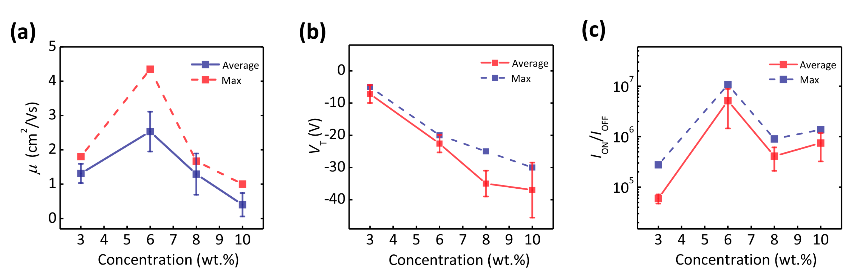
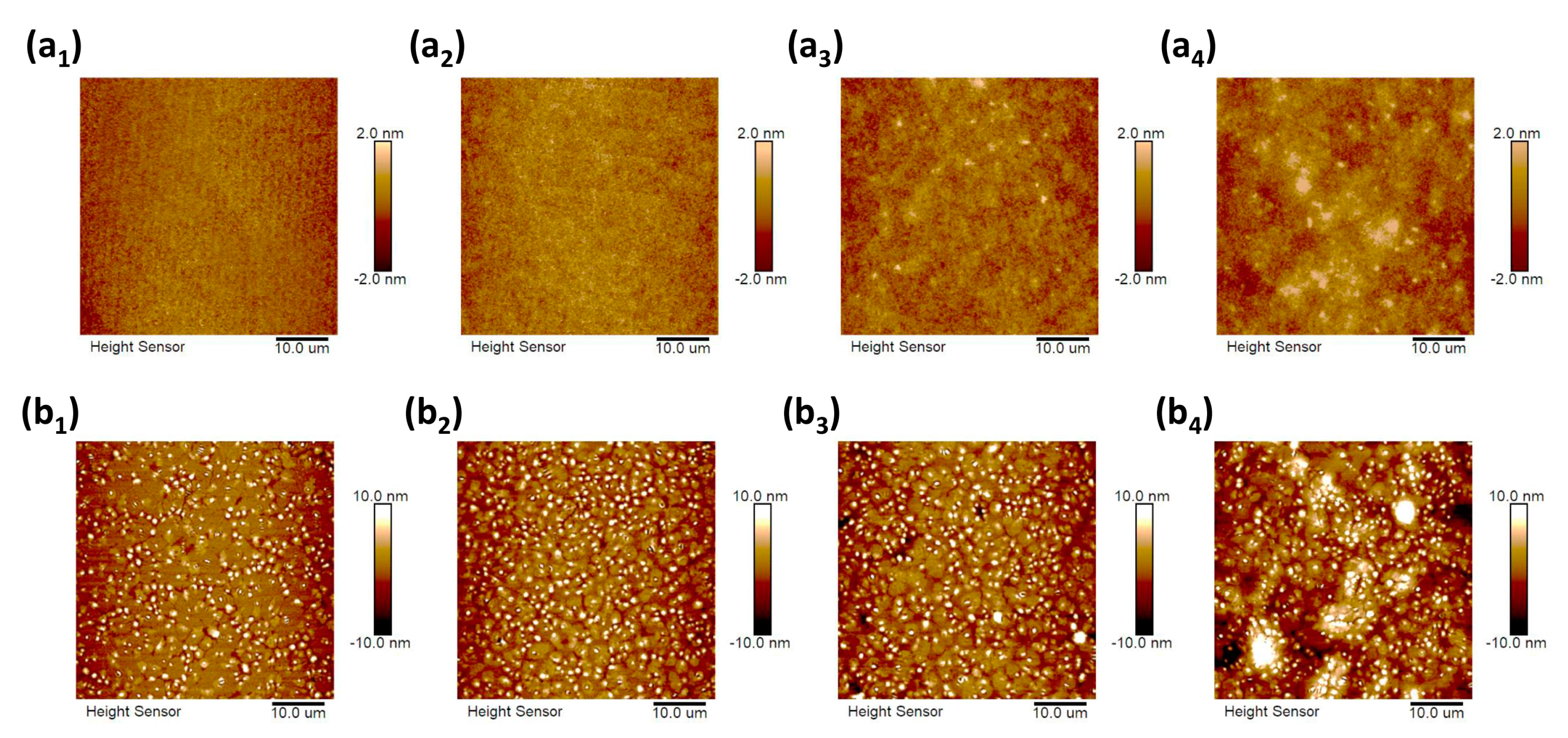
3. Results and Discussion
4. Conclusions
Supplementary Materials
Acknowledgments
Author Contributions
Conflicts of Interest
References
- Kim, D.H.; Viventi, J.; Amsden, J.J.; Xiao, J.; Vigeland, L.; Kim, Y.S.; Blanco, J.A.; Panilaitis, B.; Frechette, E.S.; Contreras, D.; et al. Dissolvable films of silk fibroin for ultrathin conformal bio-integrated electronics. Nat. Mater. 2010, 9, 511–517. [Google Scholar] [CrossRef] [PubMed]
- Martirosyan, N.; Kalani, M.Y. Epidermal electronics. Science 2011, 333, 838–845. [Google Scholar] [CrossRef] [PubMed]
- Xu, B.; Akhtar, A.; Liu, Y.; Chen, H.; Yeo, W.H.; Park, S.I.; Boyce, B.; Kim, H.; Yu, J.; Lai, H.Y.; et al. An epidermal stimulation and sensing platform for sensorimotor prosthetic control, management of lower back exertion, and electrical muscle activation. Adv. Mater. 2016, 28, 4462–4471. [Google Scholar] [CrossRef] [PubMed]
- Kim, J.; Gutruf, P.; Chiarelli, A.M.; Heo, S.Y.; Cho, K.; Xie, Z.; Banks, A.; Han, S.; Jang, K.-I.; Lee, J.W.; et al. Miniaturized battery-free wireless systems for wearable pulse oximetry. Adv. Funct. Mater. 2017, 27. [Google Scholar] [CrossRef]
- Forrest, S.R. The path to ubiquitous and low-cost organic electronic appliances on plastic. Nature 2004, 428, 911–918. [Google Scholar] [CrossRef] [PubMed]
- Eder, F.; Klauk, H.; Halik, M.; Zschieschang, U.; Schmid, G.; Dehm, C. Organic electronics on paper. Appl. Phys. Lett. 2004, 84, 2673–2675. [Google Scholar] [CrossRef]
- Rogers, J.A.; Bao, Z.; Baldwin, K.; Dodabalapur, A.; Crone, B.; Raju, V.R.; Kuck, V.; Katz, H.; Amundson, K.; Ewing, J.; et al. Paper-like electronic displays: Large-area rubber-stamped plastic sheets of electronics and microencapsulated electrophoretic inks. Proc. Natl. Acad. Sci. USA 2001, 98, 4835–4840. [Google Scholar] [CrossRef] [PubMed]
- Gelinck, G.H.; Huitema, H.E.; van Veenendaal, E.; Cantatore, E.; Schrijnemakers, L.; van der Putten, J.B.; Geuns, T.C.; Beenhakkers, M.; Giesbers, J.B.; Huisman, B.H.; et al. Flexible active-matrix displays and shift registers based on solution-processed organic transistors. Nat. Mater. 2004, 3, 106–110. [Google Scholar] [CrossRef] [PubMed]
- Rotzoll, R.; Mohapatra, S.; Olariu, V.; Wenz, R.; Grigas, M.; Dimmler, K.; Shchekin, O.; Dodabalapur, A. Radio frequency rectifiers based on organic thin-film transistors. Appl. Phys. Lett. 2006, 88. [Google Scholar] [CrossRef]
- Hammock, M.L.; Chortos, A.; Tee, B.C.; Tok, J.B.; Bao, Z. 25th anniversary article: The evolution of electronic skin (e-skin): A brief history, design considerations, and recent progress. Adv. Mater. 2013, 25, 5997–6038. [Google Scholar] [CrossRef] [PubMed]
- Sekitani, T.; Yokota, T.; Zschieschang, U.; Klauk, H.; Bauer, S.; Takeuchi, K.; Takamiya, M.; Sakurai, T.; Someya, T. Organic nonvolatile memory transistors for flexible sensor arrays. Science 2009, 326, 1516–1519. [Google Scholar] [CrossRef] [PubMed]
- Zang, Y.; Zhang, F.; Huang, D.; Gao, X.; Di, C.A.; Zhu, D. Flexible suspended gate organic thin-film transistors for ultra-sensitive pressure detection. Nat. Commun. 2015, 6. [Google Scholar] [CrossRef] [PubMed]
- Qian, Y.; Zhang, X.; Qi, D.; Xie, L.; Chandran, B.K.; Chen, X.; Huang, W. Thin-film organic semiconductor devices: From flexibility to ultraflexibility. Sci. China Mater. 2016, 59, 589–608. [Google Scholar] [CrossRef]
- Zhang, L.; Wang, H.; Zhao, Y.; Guo, Y.; Hu, W.; Yu, G.; Liu, Y. Substrate-free ultra-flexible organic field-effect transistors and five-stage ring oscillators. Adv. Mater. 2013, 25. [Google Scholar] [CrossRef] [PubMed]
- Nawrocki, R.A.; Matsuhisa, N.; Yokota, T.; Someya, T. 300-nm imperceptible, ultraflexible, and biocompatible e-skin fit with tactile sensors and organic transistors. Adv. Electron. Mater. 2016, 2. [Google Scholar] [CrossRef]
- Yi, H.T.; Payne, M.M.; Anthony, J.E.; Podzorov, V. Ultra-flexible solution-processed organic field-effect transistors. Nat. Commun. 2012, 3. [Google Scholar] [CrossRef] [PubMed]
- Fukuda, K.; Takeda, Y.; Yoshimura, Y.; Shiwaku, R.; Tran, L.T.; Sekine, T.; Mizukami, M.; Kumaki, D.; Tokito, S. Fully-printed high-performance organic thin-film transistors and circuitry on one-micron-thick polymer films. Nat. Commun. 2014, 5. [Google Scholar] [CrossRef] [PubMed]
- Diao, Y.; Tee, B.C.; Giri, G.; Xu, J.; Kim, D.H.; Becerril, H.A.; Stoltenberg, R.M.; Lee, T.H.; Xue, G.; Mannsfeld, S.C.; et al. Solution coating of large-area organic semiconductor thin films with aligned single-crystalline domains. Nat. Mater. 2013, 12, 665–671. [Google Scholar] [CrossRef] [PubMed]
- Li, H.; Tee, B.C.; Cha, J.J.; Cui, Y.; Chung, J.W.; Lee, S.Y.; Bao, Z. High-mobility field-effect transistors from large-area solution-grown aligned C60 single crystals. J. Am. Chem. Soc. 2012, 134, 2760–2765. [Google Scholar] [CrossRef] [PubMed]
- Luo, C.; Kyaw, A.K.; Perez, L.A.; Patel, S.; Wang, M.; Grimm, B.; Bazan, G.C.; Kramer, E.J.; Heeger, A.J. General strategy for self-assembly of highly oriented nanocrystalline semiconducting polymers with high mobility. Nano Lett. 2014, 14, 2764–2771. [Google Scholar] [CrossRef] [PubMed]
- Ebata, H.; Izawa, T.; Miyazaki, E.; Takimiya, K.; Ikeda, M.; Kuwabara, H.; Yui, T. Highly soluble [1]benzothieno[3,2-b]benzothiophene (BTBT) derivatives for high-performance, solution-processed organic field-effect transistors. J. Am. Chem. Soc. 2007, 129, 15732–15733. [Google Scholar] [CrossRef] [PubMed]
- Minemawari, H.; Yamada, T.; Matsui, H.; Tsutsumi, J.; Haas, S.; Chiba, R.; Kumai, R.; Hasegawa, T. Inkjet printing of single-crystal films. Nature 2011, 475, 364–367. [Google Scholar] [CrossRef] [PubMed]
- Yuan, Y.; Giri, G.; Ayzner, A.L.; Zoombelt, A.P.; Mannsfeld, S.C.; Chen, J.; Nordlund, D.; Toney, M.F.; Huang, J.; Bao, Z. Ultra-high mobility transparent organic thin film transistors grown by an off-centre spin-coating method. Nat. Commun. 2014, 5. [Google Scholar] [CrossRef] [PubMed]
- Minari, T.; Kano, M.; Miyadera, T.; Wang, S.D.; Aoyagi, Y.; Tsukagoshi, K. Surface selective deposition of molecular semiconductors for solution-based integration of organic field-effect transistors. Appl. Phys. Lett. 2009, 94. [Google Scholar] [CrossRef]
- Jang, Y.; Kim, D.H.; Park, Y.D.; Cho, J.H.; Hwang, M.; Cho, K. Low-voltage and high-field-effect mobility organic transistors with a polymer insulator. Appl. Phys. Lett. 2006, 88. [Google Scholar] [CrossRef]
- Liu, X.; Guo, Y.; Ma, Y.; Chen, H.; Mao, Z.; Wang, H.; Yu, G.; Liu, Y. Flexible, low-voltage and high-performance polymer thin-film transistors and their application in photo/thermal detectors. Adv. Mater. 2014, 26, 3631–3636. [Google Scholar] [CrossRef] [PubMed]
- Dey, A.; Kalita, A.; Krishnan Iyer, P. High-performance n-channel organic thin-film transistor based on naphthalene diimide. ACS Appl. Mater. Interfaces 2014, 6, 12295–12301. [Google Scholar] [CrossRef] [PubMed]
- Orgiu, E.; Locci, S.; Fraboni, B.; Scavetta, E.; Lugli, P.; Bonfiglio, A. Analysis of the hysteresis in organic thin-film transistors with polymeric gate dielectric. Org. Electron. 2011, 12, 477–485. [Google Scholar] [CrossRef]
- Hwang, D.K.; Lee, K.; Kim, J.H.; Im, S.; Park, J.H.; Kim, E. Comparative studies on the stability of polymer versus SiO2 gate dielectrics for pentacene thin-film transistors. Appl. Phys. Lett. 2006, 89. [Google Scholar] [CrossRef]
- Tsai, T.-D.; Chang, J.-W.; Wen, T.-C.; Guo, T.-F. Manipulating the hysteresis in poly(vinyl alcohol)-dielectric organic field-effect transistors toward memory elements. Adv. Funct. Mater. 2013, 23, 4206–4214. [Google Scholar] [CrossRef]
- Li, Y.; Liu, C.; Wang, Y.; Yang, Y.; Wang, X.; Shi, Y.; Tsukagoshi, K. Flexible field-effect transistor arrays with patterned solution-processed organic crystals. AIP Adv. 2013, 3. [Google Scholar] [CrossRef]
- Kotsuki, K.; Tanaka, H.; Obata, S.; Stauss, S.; Terashima, K.; Saiki, K. The importance of spinning speed in fabrication of spin-coated organic thin film transistors: Film morphology and field effect mobility. Appl. Phys. Lett. 2014, 104. [Google Scholar] [CrossRef]
- Uemura, T.; Hirose, Y.; Uno, M.; Takimiya, K.; Takeya, J. Very high mobility in solution-processed organic thin-film transistors of highly ordered[1]benzothieno[3,2-b]benzothiophene derivatives. Appl. Phys. Express 2009, 2. [Google Scholar] [CrossRef]


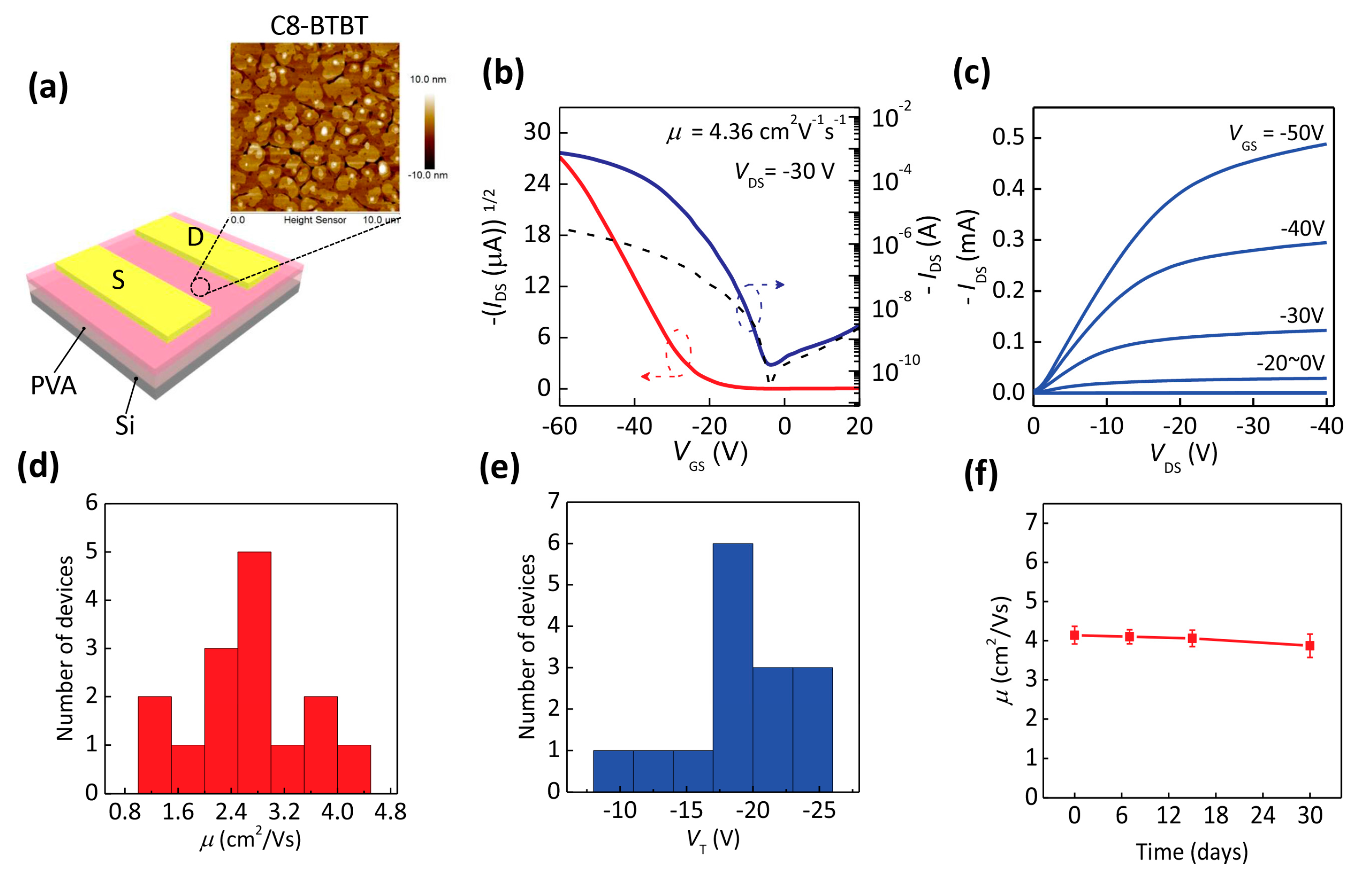
| Deformation | μ (cm2/Vs) | VT (V) | SS (V/dec) | ION/IOFF |
|---|---|---|---|---|
| on plane | 3.33 | −16 | 4.25 | 6.85 × 10⁶ |
| on the hemisphere | 3.04 | −13 | 4.34 | 4.34 × 10⁶ |
| repositioned on plane | 3.23 | −14 | 4.07 | 4.06 × 10⁶ |
© 2017 by the authors. Licensee MDPI, Basel, Switzerland. This article is an open access article distributed under the terms and conditions of the Creative Commons Attribution (CC BY) license (http://creativecommons.org/licenses/by/4.0/).
Share and Cite
Ren, H.; Tang, Q.; Tong, Y.; Liu, Y. 320-nm Flexible Solution-Processed 2,7-dioctyl[1] benzothieno[3,2-b]benzothiophene Transistors. Materials 2017, 10, 918. https://doi.org/10.3390/ma10080918
Ren H, Tang Q, Tong Y, Liu Y. 320-nm Flexible Solution-Processed 2,7-dioctyl[1] benzothieno[3,2-b]benzothiophene Transistors. Materials. 2017; 10(8):918. https://doi.org/10.3390/ma10080918
Chicago/Turabian StyleRen, Hang, Qingxin Tang, Yanhong Tong, and Yichun Liu. 2017. "320-nm Flexible Solution-Processed 2,7-dioctyl[1] benzothieno[3,2-b]benzothiophene Transistors" Materials 10, no. 8: 918. https://doi.org/10.3390/ma10080918
APA StyleRen, H., Tang, Q., Tong, Y., & Liu, Y. (2017). 320-nm Flexible Solution-Processed 2,7-dioctyl[1] benzothieno[3,2-b]benzothiophene Transistors. Materials, 10(8), 918. https://doi.org/10.3390/ma10080918