Article

Impacts of the Oxygen Precursor on the Interfacial Properties of LaxAlyO Films Grown by Atomic Layer Deposition on Ge

Key Laboratory for Wide Band Gap Semiconductor Materials and Devices of Education, School of Microelectronics, Xidian University, Xi’an 710071, China
*
Author to whom correspondence should be addressed.
Materials 2017, 10(8), 856; https://doi.org/10.3390/ma10080856
Submission received: 28 June 2017 / Revised: 14 July 2017 / Accepted: 22 July 2017 / Published: 26 July 2017

Abstract

:
Amorphous LaxAlyO films were grown on n-type Ge substrate by atomic layer deposition using O3 and H2O as oxidant, respectively. A comparison of the XPS results indicated that a thicker interfacial layer with the component of LaGeOx and GeOx was formed at O3-based LaxAlyO/Ge interface, causing lower band gap value as well as the conduction band offset (CBO) value relative to Ge substrate for O3-based LaxAlyO film, with a concomitant degeneration in the interfacial properties. In contrast, for the H2O-based film, the leakage current of more than one order of magnitude less than that of O3-based LaxAlyO film was obtained. All the results indicated that H2O is a more appropriate oxidant for improving the interfacial properties in the atomic-layer-deposited LaxAlyO dielectric on Ge.

1. Introduction

With Si-based complementary-metal-oxide-semiconductor (CMOS) devices approaching their fundamental limits, high dielectric constant (high-k) materials grown on germanium and other high mobility semiconductors have been investigated to increase the drain current in the channel region [1,2]. Unfortunately, one primary challenge for Ge used in MOSFET devices is generally the poor electrical performance of native Ge oxide, resulting in poor interfacial properties at the insulator/Ge interface for most high-k dielectrics deposited on Ge substrate without any surface passivation process [3,4]. In order to improve the interface quality, appropriate passivation should be carried out. Attentions had been focused on the formation of thermally grown GeO2 prior to the high-k dielectrics deposition process [5,6]. However, GeO2 becomes unstable at high temperature when deposited on Ge because it would react with Ge atoms to form substoichiometric oxide or volatile GeO [7,8], deteriorating the electrical performance of Ge-based MOS devices. Recently, rare earth oxides have been considered as a promising passivation interlayer for high-k dielectric grown on Ge [9]. Furthermore, La-based dielectric materials have been shown to form a good passivation layer due to the formation of a stable La germanate compound on Ge substrate which could prevent the formation of volatile GeO [10,11]. Among various deposition methods for growing high-k dielectric films, atomic layer deposition (ALD) has been considered as one of the most promising technique to produce high-k dielectric films in high quality due to the outstanding characteristics for precise thickness and composition control, excellent uniformity and process compatibility to conventional CMOS process [12,13]. O3 and H2O are two kinds of oxygen source precursors commonly used in the ALD process. It has been reported that the difference of oxidants would have an impact on the ALD reaction mechanism and surface chemistry of the deposited film [14], with a further influence on the relative electrical properties.
In this paper, the effect of H2O and O3 on the interfacial properties of LaxAlyO films grown by atomic layer deposition on Ge was systematically investigated. X-ray photoelectron spectroscopy (XPS) analysis of the LaAlO3 films was used to provide direct observation on the band alignments of LaxAlyO films relative to Ge substrate. Attentions were focused on the electrical performance of LaxAlyO/Ge structures to analyze the influence of different oxygen precursors on the interfacial properties.

2. Experiment

LaxAlyO gate dielectric films were deposited on n-type Ge (100) wafers with resistivity of 0.1–1 Ω·cm by ALD technique using La(i−PrCp)3 and TMA as La and Al precursor, while two kinds of oxygen source precursors (O3 and H2O) were used as oxidant, respectively. Prior to the deposition, Ge substrates were treated with acetone and hydrous alcohol, and then dipped into 2%-HF solution for 30 s to remove the native GeOx layer, followed by a 60 s rinse in de-ionized water. The precursors were alternately introduced to the reactor chamber using high purity N2 (>99.999%) as the carrier gas. A typical ALD growth cycle for La2O3 with O3 used as the oxygen precursor was 0.1 s La(i−PrCp)3 pulse/4 s N2 purge/0.3 s O3 pulse/10 s N2 purge, whereas for Al2O3 with O3 used as the oxygen precursor, it was 0.1 s TMA pulse/3 s N2 purge/0.5 s O3 pulse/4 s N2 purge. Moreover, when H2O was used as the oxygen precursor, a typical ALD growth cycle for La2O3 was set as 0.3 s La(i−PrCp)3 pulse/4 s N2 purge/ 0.3 s H2O pulse/9 s N2 purge, while for Al2O3, it was 0.1 s TMA pulse/3 s N2 purge/0.1 s H2O pulse/4 s N2 purge. Using these process parameters, for La2O3, a linear relation with a growth rate of approximately 0.85 Å/cycle was obtained, and the steady-state growth rate of Al2O3 films was approximately 0.93 Å/cycle with O3 as the oxygen precursor. Besides, when H2O was used as the oxidant, the growth thickness per ALD cycle for La2O3 was ~0.75 Å, while the growth rate of Al2O3 was approximately 0.92 Å/cycle. At the deposition temperature of 300 °C, the film thickness was tuned to fix at ~10 nm and ~5 nm by varying the number of ALD cycles while setting the La/Al pulse ratio as 1:1.
Post-deposition rapid thermal annealing was carried out at 600 °C for 90 s in N2 ambient. The crystallization characteristics of the LaxAlyO films were checked by grazing incidence X-ray Diffraction (GIXRD) at the angle of incidence ω = 0.5°. None of the films reveal any diffraction peaks, indicating in the thermal stability of the films. The physical thickness of the deposited films was optically measured using Woollam M2000U (Woollam Co. Inc., Lincoln, NE, USA) spectroscopic ellipsometry (SE) by fitting the ellipsometry data using a Gen-Osc mode consisting of Gaussian and Tauc-Lorentz oscillators and considering the native GeOx. The composition and band structure of the deposited LaxAlyO films was examined by XPS measurements. All the wafers were etched by Ar+ ion beam bombardment for 10 s (~0.26 nm/s) to remove the influence of the impurities on the surface. C 1s peak from adventitious carbon at 284.6 eV was used as an internal energy reference during the XPS analysis. In this experiment, the ~10 nm LaxAlyO film was used to obtain the XPS spectra for thick amorphous LaxAlyO, and the ~5 nm LaxAlyO/Ge structure was thin enough to obtain XPS spectra from both the LaxAlyO film and the underlying germanium substrate. The electrical properties of the 5 nm films were measured using a metal-insulator-semiconductor (MIS) capacitor structure. A metal gate with a diameter of 300 μm was fabricated by depositing 150 nm Al using the electron-beam evaporation through a shadow mask, followed by annealing in forming gas ambient (97% N2/3% H2) at 400 °C for 20 min. The capacitance-voltage (C-V) and leakage current density-voltage (J-V) measurements were carried out using Agilent B1500A analyzer.

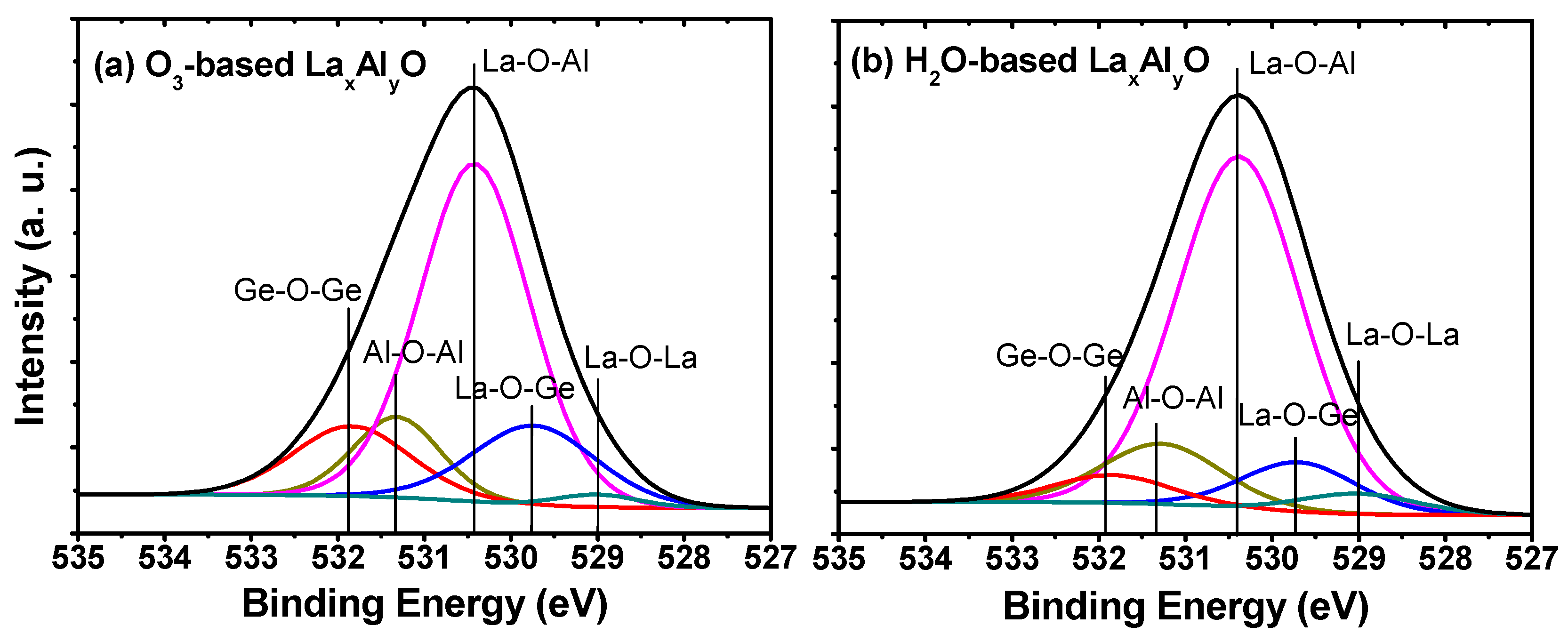
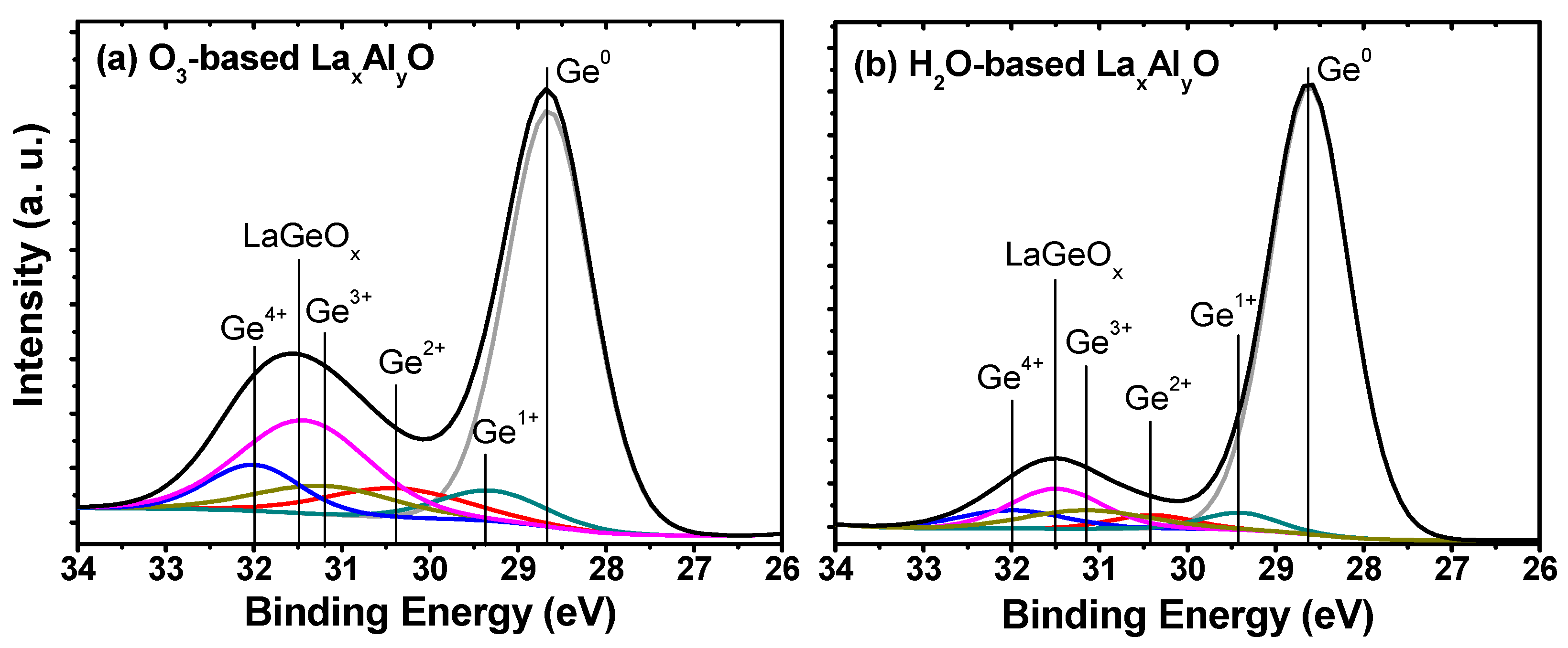
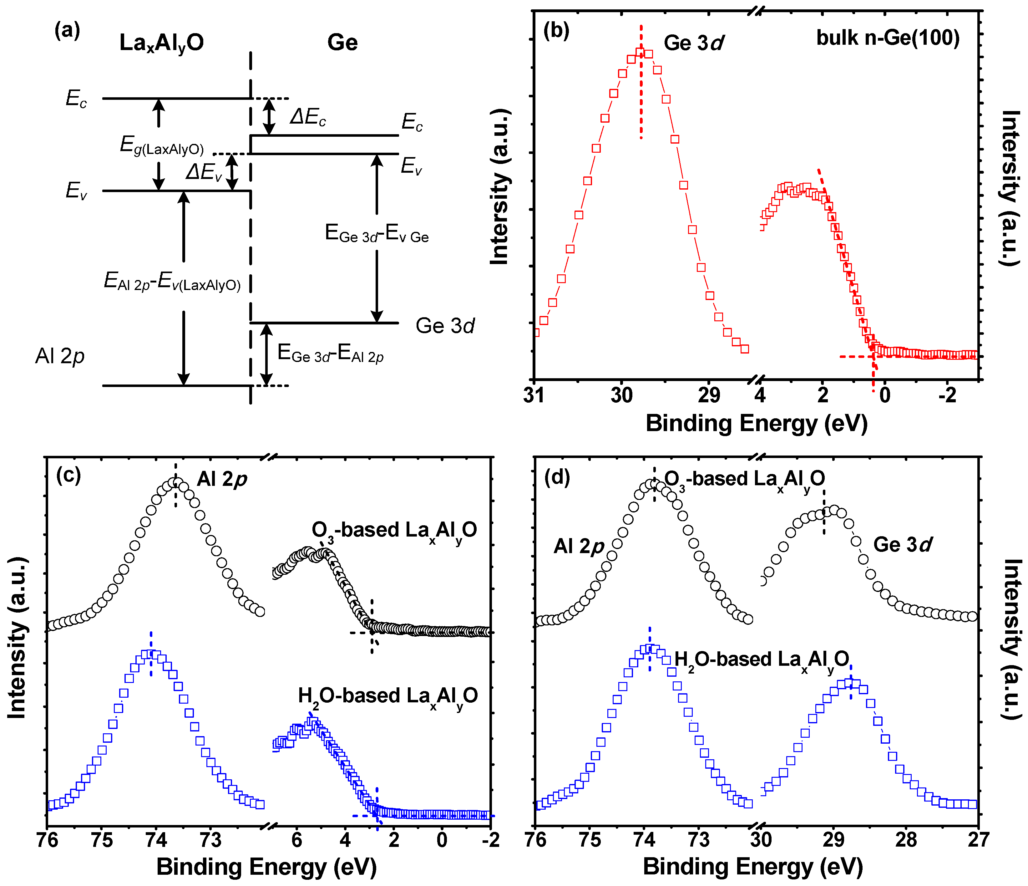
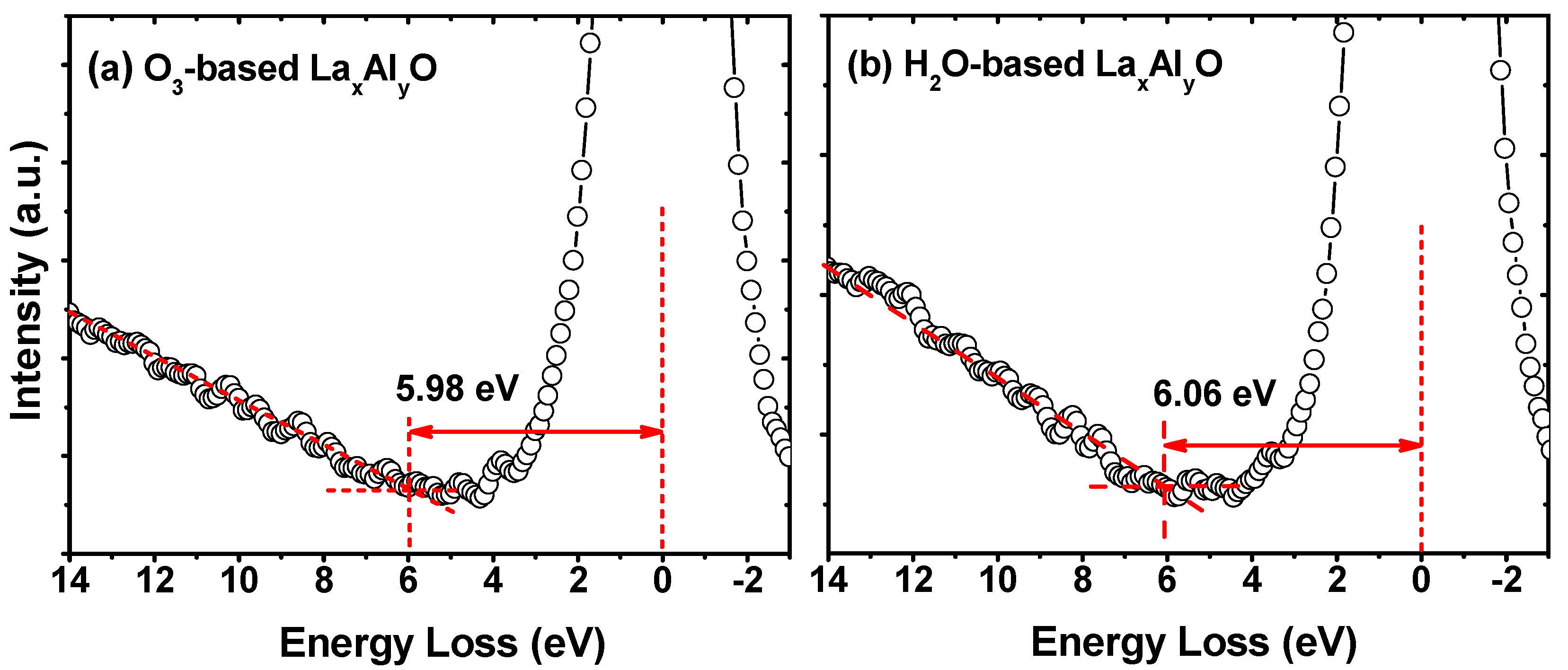
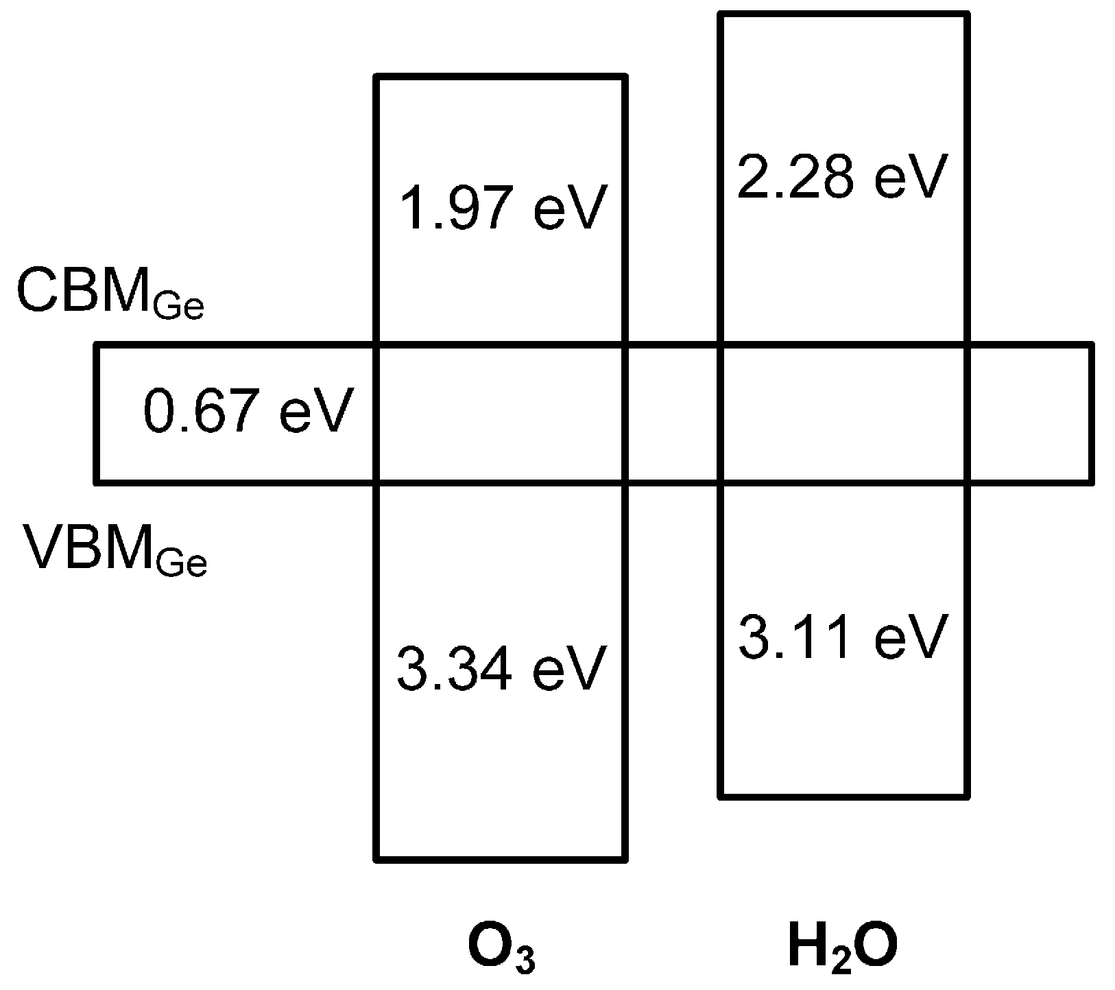
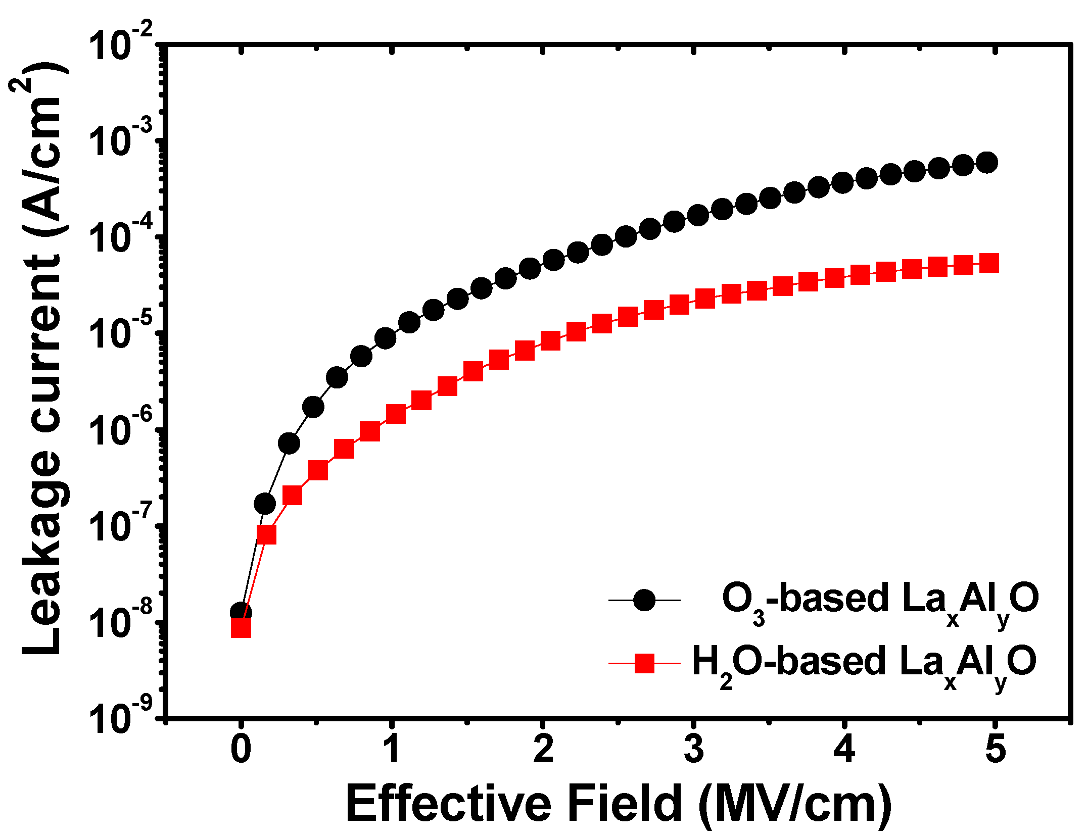
3. Results and Discussion

As shown in Figure 1, the variations in O 1s XPS spectra for the 5 nm O3-based and H2O-based LaxAlyO films annealed at 600 °C were analyzed to investigate the chemical bonding states near the LaxAlyO film and Ge substrate interfaces. The O 1s spectra were fitted with five Gaussian–Lorentzian line-shaped peaks, which are at 529.0, 529.7, 530.4, 531.3 and 531.9 eV. These peaks correspond to the chemical bonds of La-O-La, La-O-Ge, La-O-Al, Al-O-Al and Ge-O-Ge, respectively [15,16,17]. For La-O-La, La-O-Al and Al-O-Al chemical bonds; the intensity of the peaks varies slightly, indicating the difference of oxidant has negligible influence on the chemical bond structures of the upper deposited LaxAlyO layers. However, compared with the LaxAlyO film using H2O as oxidant, an obvious increment in the intensity of La-O-Ge and Ge-O-Ge peaks could be observed for the O3-based LaxAlyO film, which illustrates that more interfacial oxide layer (mainly consisting of LaGeOx and GeOx) was formed at the O3-based LaxAlyO/Ge interface during the deposition and post-deposition annealing process [18], which may be caused by the higher oxidability of O3 [19].
In order to study the chemical bonding states near the LaxAlyO film and Ge substrate interfaces more clearly, further investigation was applied to the variations in Ge 3d XPS spectra for the 5 nm O3-based and H2O-based LaxAlyO films, as shown in Figure 2. The Ge oxide (GeOx) spectra, which are located at a higher binding energy with respect to the Ge0 peak originating from the Ge substrate, can be deconvoluted into four GeOx peaks (Ge1+, Ge2+, Ge3+, Ge4+) with energy shift of 0.8, 1.8, 2.6, and 3.4 eV, respectively. These GeOx species were likely present due to the formation of an interfacial layer between the LaxAlyO film and Ge substrate. Here, the Ge4+ peak originates from GeO2, and other Ge1+, Ge2+ and Ge3+ peaks originate from Ge sub-oxides [20]. A comparison of Figure 2a,b revealed the same variation trend of the formation of interfacial oxide layer as analysed in the O 1s XPS spectra; that is, larger amounts of LaGeOx and GeOx, including GeO2 and Ge sub-oxides, were formed at LaxAlyO/Ge interface in the O3-based case. The variation of these interfacial oxides would have an influence on the interfacial characteristics of LaxAlyO film/Ge structure and then affect its electrical properties, and this aspect will be discussed in detail later in this paper.
The band offsets of LaxAlyO films relative to the Ge substrate were determined by a core level photoemission-based method similar to that of Kraut et al. [21,22], as illustrated in Figure 3a. Accordingly, the valence band offset (VBO, ΔEv) is given by Equation (1):
Δ E v = ( E Ge   3 d E V ) Ge ( E Al   2 p E V ) Thick   La x Al y O ( E Ge   3 d E Al   2 p ) La x Al y O / Ge
where ( E Ge   3 d E V ) Ge is the energy difference between Ge 3d and valence band maximum (VBM) in the bulk clean Ge substrate, as shown in Figure 3b; ( E Al   2 p E V ) Thick   La x Al y O is the energy difference between Al 2p and VBM in the 10 nm LaxAlyO film, as shown in Figure 3c; and ( E Ge   3 d E Al   2 p ) La x Al y O / Ge is the energy difference between Ge 3d and Al 2p core levels in the 5 nm LaxAlyO on n-Ge(100), as shown in Figure 3d. Then, according to Equation (1), the VBOs for the films with O3 and H2O as oxidant can be figured out as 3.34 and 3.11 eV, respectively.
The corresponding conduction band offset (CBO, ΔEc) between LaxAlyO and Ge can be obtained by Equation (2):
Δ E c = E g ( La x Al y O ) Δ E v E g ( Ge )
It is generally known that the band gap of germanium is 0.67 eV at room temperature. In order to obtain the CBOs of LaxAlyO films relative to germanium, the band gap of amorphous LaxAlyO on Ge substrate needs to be determined.
The band gaps of LaxAlyO films were measured by examining the energy loss of the O 1s core levels for the 10 nm samples by XPS measurements. After being etched for ~2 nm, the XPS spectra signals can be considered as coming from the pure deposited films. In principle, the photoexcited electrons passing through dielectric films can suffer inelastic losses due to plasmon (collective oscillation) and single particle excitation (band-to-band transition excitation) [23]. It is proved that the band gap equals the energy distance between the photoemission peak centroid and the onset of the features due to single particle excitations, and it is usually obtained from the inelastic energy loss features observed on the high binding energy side of the core level photoemission peaks [24]. Besides, the onset of the O 1s loss spectrum can be determined by linearly extrapolating the segment of maximum negative slope to the background level [25,26]. Using this method, as shown in Figure 4, the band gaps of the O3-based and H2O-based LaxAlyO films were determined to be 5.98 and 6.06 eV, respectively. Accordingly, the CBOs of O3-based and H2O-based LaxAlyO films relative to Ge were figured out as 1.97 and 2.28 eV, respectively.
Results of the calculated band gaps and band offsets are shown in the schematic diagram in Figure 5. It is worth noting that the band gap values of the deposited LaxAlyO films are smaller than those of pure amorphous LaxAlyO film of ~6.2 eV [27], which implies that the composition of the deposited film is not pure LaxAlyO. As is known; to some extent, the influence of the XPS signals from the possible interfacial oxide layer (GeO2, Eg ~ 5.8 eV) would diminish the band gap values of the deposited LaxAlyO films [28]. Thus, the variation of the band gaps would reflect the degree of the formation of interfacial oxide layer between the deposited LaxAlyO film and Ge substrate. That is, a thicker interfacial oxide layer should exist at the O3-based LaxAlyO/Ge interface, as the band gap of O3-based LaxAlyO film is slightly smaller than that of the H2O-based sample. This result is in good agreement with the interfacial chemical bonds information extracted from the O 1s and Ge 3d spectra as mentioned above. In addition, the CBO of GeO2 relative to Ge (~0.54 eV) is much smaller than that of LaxAlyO on Ge (~2.2 eV) [28,29]. Consequently, due to the existence of a thinner interfacial layer, a bigger value of CBO is obtained when H2O was used as oxidant.
Figure 6 shows the C-V characteristics of the fabricated MIS capacitors using 5 nm O3-based and H2O-based LaxAlyO films as insulators. For simplicity, the MIS capacitor structures using O3-based and H2O-based LaxAlyO films as insulators were assigned as MIS capacitor S1 and MIS capacitor S2, respectively. The C-V curves were obtained by sweeping forward (bias from negative to positive) and backward (bias from positive to negative) at a frequency of 100 kHz. The flat band voltages (VFB) of the C-V curves were extracted from the simulation software Hauser NCSU CVC program, taking into account quantum mechanical effects [30]. Compared with MIS capacitor S2, a positive VFB shift could be observed in the C-V curves for MIS capacitor S1, which is an indication of the presence of more effective negative oxide charges in the bulk of the O3-based gate dielectric. Ruling out the influence of generally positive charged fixed oxide charges (Qf) and mobile ionic charges (Qm), the oxide trapped charges (Qot) negative charged were suspected to be responsible for the positive shift of VFB [31]. The charge trapping behavior of the fabricated capacitors was investigated through the C-V hysteresis characteristics. The hysteresis width (ΔVFB) extracted from the dual-swept C-V curves for MIS capacitors S1 and S2 are 154 and 95 mV, respectively. For the O3-based sample, a larger ΔVFB of the dual-swept C-V curves illustrates the existence of more oxide trapped charges in the O3-based gate dielectric, which is in consistent with the shift tendency of VFB. Additionally, it is worth noting that, compared with what is shown in Figure 6b, the C-V curves for MIS capacitor S1 (Figure 6a) slope gently and exhibit a more obvious anomalous hump phenomenon in the weak inversion region, indicating the formation of more interface traps at the O3-based LaxAlyO film/Ge interface.
From the XPS results as mentioned above, we can conclude that a thicker interfacial layer consisting of LaGeOx and GeOx exists between O3-based LaxAlyO film and Ge substrate. Such an interfacial layer, as reported, has a much lower dielectric constant (5~6) than that of LaxAlyO [32,33], resulting in a smaller accumulation capacitance value for MIS capacitor S1. Being a thermally stable germanate compound on the surface of Ge substrate, LaGeOx was reported to be of help in suppressing Ge out-diffusion and improving interface quality. However, among the germanium oxides, GeO is volatile and sublimes leaving behind a defective interface contained lots of defects and dangling bonds, which makes it known to have an adverse influence on the interfacial properties [11]. Additionally, it has been reported that at temperatures of up to 430 °C, GeO2 becomes unstable, and will react with substrate Ge atoms generating volatile GeO, following the reaction of GeO2 + Ge → 2GeO [7]. Therefore, compared with the H2O-based LaxAlyO, the increase in oxide-trapped charges and interface traps in O3-based LaxAlyO film/Ge structures should be attributed to the extra formation of volatile GeO.
Figure 7 shows the leakage current density as a function of the applied electrical field for the fabricated Al/5 nm LaxAlyO/n-type Ge capacitor structure. As we know, the polarity of gate leakage current through gate dielectrics depends on the gate bias polarity and substrate doping type. For the n-type Ge substrate used in this work, electron injection from the conduction band is the dominant tunneling current component under positive gate bias [34]. At the applied electrical field of 3 MV/cm, the leakage current density of the O3-based and H2O-based film was measured to be 2.29 × 10⁻⁵ and 1.68 × 10⁻⁴ A/cm2, separately. Compared with the O3-based LaxAlyO film, a decrease of more than one order of magnitude in the leakage current density was found for the H2O-based film. Such a decrease is suspected of benefiting from the larger conduction band offset mentioned above. The larger conduction band offset means the existence of higher potential barriers between the LaxAlyO film and n-Ge substrate, which would weaken the tunneling effect of electrons in the MIS capacitors, resulting in lower gate leakage current. In addition, less structural defects and dangling bonds in the H2O-based LaxAlyO film/Ge structure mean a smaller possibility to create a conduction path by forming a continuous chain connecting the gate to the semiconductor, which may also provide an explanation for the significant decrease of gate leakage current in MIS capacitors S2.

4. Conclusions

In this paper, amorphous LaxAlyO films were deposited on Ge substrate by ALD using O3 and H2O as oxygen precursor, respectively. Due to the higher oxidability of O3, the formation of interfacial layer (mainly consisting of LaGeOx and GeOx) was enhanced at O3-based LaxAlyO/Ge interface, leading to a slight decrease of the band gap for O3-based LaxAlyO film, as well as the CBO value relative to Ge substrate compared with that of the H2O-based sample. Additionally, the extra formation of volatile GeO causes the increase of oxide trapped charges and interface traps in O3-based LaxAlyO film/Ge structure. As a result, a much lower gate leakage current was obtained when the H2O-based LaxAlyO film was used as MIS gate insulator, indicating that H2O is a more appropriate oxidant applied for the deposition of LaxAlyO dielectric on Ge substrate to achieve suitable band alignments and favorable interfacial properties.

Acknowledgments

The work described in this paper was fully supported by grants from the National Natural Science Foundation of China (Grant No. 61376099), the Foundation for Fundamental Research of China (Grant No. JSZL2016110B003) and the Key Fundamental Research Program of Shaanxi Province (Grant No. 2017ZDJC-26).

Author Contributions

Lu Zhao generated the research idea, analyzed the data, and wrote the paper. Lu Zhao and Xing Wang carried out the experiments and the measurements. Yongte Wang and Shulong Wang participated in the discussions. Hongxia Liu gave the final approval of the version to be published. All authors read and approved the final manuscript.

Conflicts of Interest

The authors declare no conflict of interest.

References

  1. Yi, S.H.; Chang-Liao, K.S.; Wu, T.Y.; Hsu, C.W.; Huang, J.Y. High performance Ge pMOSFETs with HfO2/Hf-Cap/GeOx gate stack and suitable post metal annealing treatments. IEEE Electron Device Lett. 2017, 38, 544–547. [Google Scholar] [CrossRef]
  2. Xie, Q.; Deng, S.; Schaekers, M.; Lin, D.; Caymax, M.; Delabie, A.; Qu, X.P.; Jiang, Y.L.; Deduytsche, D.; Detavernier, C. Germanium surface passivation and atomic layer deposition of high-k dielectrics—A tutorial review on Ge-based MOS capacitors. Semicond. Sci. Technol. 2012, 27, 074012. [Google Scholar] [CrossRef]
  3. Seok, T.J.; Cho, Y.J.; Jin, H.S.; Kim, D.H.; Kim, D.W.; Lee, S.M.; Park, J.B.; Won, J.Y.; Kim, S.K.; Hwang, C.S.; et al. High quality interfacial sulfur passivation via H2S pre-deposition annealing for an atomic-layer-deposited HfO2 film on a Ge substrate. J. Mater. Chem. C 2016, 4, 850–856. [Google Scholar] [CrossRef]
  4. Simoen, E.; Mitard, J.; Hellings, G.; Eneman, G.; DeJaeger, B.; Witters, L.; Vincent, B.; Loo, R.; Delabie, A.; Sioncke, S.; et al. Challenges and opportunities in advanced Ge pMOSFETs. Mat. Sci. Semicon. Proc. 2012, 15, 588–600. [Google Scholar] [CrossRef]
  5. Yoshida, T.; Kato, K.; Shibayama, S.; Sakashita, M.; Taoka, N.; Takeuchi, W.; Nakatsuka, O.; Zaima, S. Interface properties of Al2O3/Ge structures with thin Ge oxide interfacial layer formed by pulsed metal organic chemical vapor deposition. Jpn. J. Appl. Phys. 2014, 53, 08LD03. [Google Scholar] [CrossRef]
  6. Bethge, O.; Henkel, C.; Abermann, S.; Pozzovivo, G.; Stoeger-Pollach, M.; Werner, W.S.M.; Smoliner, J.; Bertagnolli, E. Stability of La2O3 and GeO2 passivated Ge surfaces during ALD of ZrO2 high-k dielectric. Appl. Surf. Sci. 2012, 258, 3444–3449. [Google Scholar] [CrossRef]
  7. Sahari, S.K.; Ohta, A.; Matsui, M.; Mishima, K.; Murakami, H.; Higashi, S.; Miyazak, S. Kinetics of thermally oxidation of Ge(100) surface. J. Phys. Conf. Ser. 2013, 417, 012014. [Google Scholar] [CrossRef]
  8. Wang, S.K.; Kita, K.; Lee, C.H.; Tabata, T.; Nishimura, T.; Nagashio, K.; Toriumi, A. Desorption kinetics of GeO from GeO2/Ge structure. J. Appl. Phys. 2010, 105, 054104. [Google Scholar]
  9. Mitrovic, I.Z.; Althobaiti, M.; Weerakkody, A.D.; Dhanak, V.R.; Linhart, W.M.; Veal, T.D.; Sedghi, N.; Hall, S.; Chalker, P.R.; Tsoutsou, D.; et al. Ge interface engineering using ultra-thin La2O3 and Y2O3 films: A study into the effect of deposition temperature. J. Appl. Phys. 2014, 115, 114102. [Google Scholar] [CrossRef]
  10. Li, X.F.; Liu, X.J.; Cao, Y.Q.; Li, A.D.; Li, H.; Wu, D. Improved interfacial and electrical properties of atomic layer deposition HfO2 films on Ge with La2O3 passivation. Appl. Surf. Sci. 2013, 264, 783–786. [Google Scholar] [CrossRef]
  11. Bethge, O.; Zimmermann, C.; Lutzer, B.; Simsek, S.; Abermann, S.; Bertagnolli, E. ALD grown rare-earth high-k oxides on Ge: Lowering of the interface trap density and EOT scalability. ECS Trans. 2014, 64, 69–76. [Google Scholar] [CrossRef]
  12. Yang, W.; Sun, Q.Q.; Fang, R.C.; Chen, L.; Zhou, P.; Ding, S.J.; Zhang, D.W. The thermal stability of atomic layer deposited HfLaOx: Material and electrical characterization. Curr. Appl. Phys. 2012, 12, 1445–1447. [Google Scholar] [CrossRef]
  13. Baitimirova, M.; Viter, R.; Andzane, J.; Lee, A.V.D.; Voiry, D.; Iatsunskyi, I.; Coy, E.; Mikoliunaite, L.; Tumenas, S.; Załęski, K.; et al. Tuning of structural and optical properties of Graphene/ZnO nanolaminates. J. Phys. Chem. C 2016, 120, 23716–23725. [Google Scholar] [CrossRef]
  14. Wiemer, C.; Lamagna, L.; Fanciulli, M. Atomic layer deposition of rare-earth-based binary and ternary oxides for microelectronic applications. Semicond. Sci. Technol. 2012, 27, 251–264. [Google Scholar] [CrossRef]
  15. Lee, B.H.; Oh, J.; Tseng, H.H.; Jammy, R.; Huff, H. The effects of annealing ambient on the characteristics of La2O3 films deposited by RPALD. J. Electrochem. Soc. 2010, 157, H479–H482. [Google Scholar]
  16. Ali, K.; Choi, K.H.; Jo, J.; Yun, W.L. High rate roll-to-roll atmospheric atomic layer deposition of Al2O3 thin films towards gas diffusion barriers on polymers. Mater. Lett. 2014, 136, 90–94. [Google Scholar] [CrossRef]
  17. Song, J.; Kakushima, K.; Ahmet, P.; Tsutsui, K.; Sugii, N.; Hattori, T.; Iwai, H. Improvement of interfacial properties with interfacial layer in La2O3/Ge structure. Microelectron. Eng. 2007, 84, 2336–2339. [Google Scholar] [CrossRef]
  18. Delabie, A.; Alian, A.; Bellenger, F.; Caymax, M.; Conard, T.; Franquet, A.; Sioncke, S.; Elshocht, V.S.; Heyns, M.M.; Meuris, M. H2O- and O3-based atomic layer deposition of high-κ dielectric films on GeO2 passivation layers. J. Electrochem. Soc. 2009, 156, G163–G167. [Google Scholar] [CrossRef]
  19. Spiga, S.; Wiemer, C.; Tallarida, G.; Scarel, G.; Ferrari, S.; Seguini, G.; Fanciulli, M. Effects of the oxygen precursor on the electrical and structural properties of HfO2 films grown by atomic layer deposition on Ge. Appl. Phys. Lett. 2005, 87, 112904. [Google Scholar] [CrossRef]
  20. Oh, I.K.; Kim, M.K.; Lee, J.S.; Lee, C.W.; Lansalot-Matras, C.; Noh, W.; Park, J.; Noorid, A.; Thompson, D.; Chu, S.; et al. The effect of La2O3-incorporation in HfO2 dielectrics on Ge substrate by atomic layer deposition. Appl. Surf. Sci. 2013, 287, 349–354. [Google Scholar] [CrossRef]
  21. Kraut, E.A.; Grant, R.W.; Waldrop, J.R.; Kowalczyk, S.P. Precise determination of the valence-band edge in X-Ray photoemission spectra: Application to measurement of semiconductor interface potentials. Phys. Rev. Lett. 1980, 44, 1620. [Google Scholar] [CrossRef]
  22. Kraut, E.A.; Grant, R.W.; Waldrop, J.R.; Kowalczyk, S.P. Semiconductor core-level to valence-band maximum binding-energy differences: Precise determination by X-ray photoelectron spectroscopy. Phys. Rev. B 1983, 28, 1965. [Google Scholar] [CrossRef]
  23. Zhu, Y.; Jain, N.; Mohata, D.K.; Datta, S.; Lubyshev, D.; Fastenau, J.M.; Liu, A.K.; Hudait, M.K. Band offset determination of mixed As/Sb type-II staggered gap heterostructure for n-channel tunnel field effect transistor application. J. Appl. Phys. 2013, 113, 024319. [Google Scholar] [CrossRef]
  24. Liu, Q.Y.; Fang, Z.B.; Liu, S.Y.; Tan, Y.S.; Chen, J.J. Band offsets of La2O3 films on Ge substrates grown by radio frequency magnetron sputtering. Mater. Lett. 2014, 116, 43–45. [Google Scholar] [CrossRef]
  25. Suzuki, M. Comprehensive study of lanthanum aluminate high-dielectric-constant gate oxides for advanced CMOS devices. Materials 2012, 5, 443–477. [Google Scholar] [CrossRef]
  26. Viter, R.; Iatsunskyi, I.; Fedorenko, V.; Tumenas, S.; Balevicius, Z.; Ramanavicius, A.; Balme, S.; Kempiński, M.; Nowaczyk, G.; Jurga, S.; et al. Enhancement of electronic and optical properties of ZnO/Al2O3 nanolaminate coated electrospun nanofibers. J. Phys. Chem. C 2016, 120, 5124–5132. [Google Scholar] [CrossRef]
  27. Edge, L.F.; Schloma, D.G. Measurement of the band offsets between amorphous LaAlO3 and silicon. Appl. Phys. Lett. 2004, 84, 726. [Google Scholar] [CrossRef] [Green Version]
  28. Perego, M.; Scarel, G.; Fanciulli, M.; Fedushkin, I.L.; Skatova, A.A. Fabrication of GeO2 layers using a divalent Ge precursor. Appl. Phys. Lett. 2007, 90, 162115. [Google Scholar] [CrossRef]
  29. Mi, Y.Y.; Wang, S.J.; Chai, J.W.; Pan, J.S.; Huan, A.C.H.; Ning, M.; Ong, C.K. Energy-band alignments at LaAlO3 and Ge interfaces. Appl. Phys. Lett. 2006, 89, 202107. [Google Scholar] [CrossRef]
  30. Hauser, J.R.; Ahmed, K. Characterization of ultra-thin oxides using electrical C-V and I-V measurements. AIP Conf. Proc. 1998, 449, 235. [Google Scholar]
  31. SZE, S.M.; NG, K.K. Physics of Semiconductor Devices, 3rd ed.; John Wiley & Sons Inc.: Hoboken, NJ, USA, 2006; pp. 223–236. [Google Scholar]
  32. Lamagna, L.; Wiemer, C.; Perego, M.; Volkos, S.N.; Baldovino, S.; Tsoutsou, D.; Schamm-Chardon, S.; Coulon, P.E.; Fanciulli, M. O3-based atomic layer deposition of hexagonal La2O3 films on Si(100) and Ge(100) substrates. J. Appl. Phys. 2010, 108, 084108. [Google Scholar] [CrossRef]
  33. Swaminathan, S.; Sun, Y.; Pianetta, P.; McIntyre, P.C. Ultrathin ALD-Al2O3 layers for Ge(001) gate stacks: Local composition evolution and dielectric properties. J. Appl. Phys. 2011, 110, 094105. [Google Scholar] [CrossRef]
  34. Ando, T. Ultimate scaling of high-κ gate dielectrics: Higher-κ or interfacial layer scavenging? Materials 2012, 5, 478–500. [Google Scholar] [CrossRef]
Figure 1. Shallow core-level spectra of O 1s for the 5 nm (a) O3-based and (b) H2O-based LaxAlyO films.
Materials 10 00856 g001
Figure 2. Shallow core-level spectra of Ge 3d for the 5 nm (a) O3-based and (b) H2O-based LaxAlyO films.
Materials 10 00856 g002
Figure 3. (a) schematic of band energy alignment diagram for a LaxAlyO/Ge structure; XPS core level spectra of (b) Ge 3d and valence band for bulk clean n-Ge(100); (c) Al 2p and valence band for 10 nm LaxAlyO films; and (d) Al 2p and Ge 3d for 5 nm LaxAlyO films on n-Ge(100).
Materials 10 00856 g003
Figure 4. O 1s energy-loss spectra for the 10 nm (a) O3-based and (b) H2O-based LaxAlyO films.
Materials 10 00856 g004
Figure 5. Results of the calculated band offsets for the LaxAlyO/Ge structures with O3 and H2O as oxidant.
Materials 10 00856 g005
Figure 6. C-V characteristics of MIS capacitors using 5 nm (a) O3-based and (b) H2O-based LaxAlyO films as insulators.
Materials 10 00856 g006
Figure 7. J-V characteristics of MIS capacitors using 5 nm O3-based and H2O-based LaxAlyO films as insulators.
Materials 10 00856 g007

