Shallow V-Shape Nanostructured Pit Arrays in Germanium Using Aqua Regia Electroless Chemical Etching


Abstract
:
1. Introduction
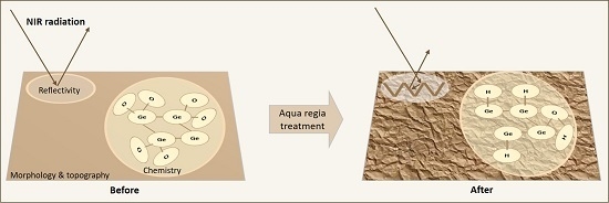
2. Results and Discussion
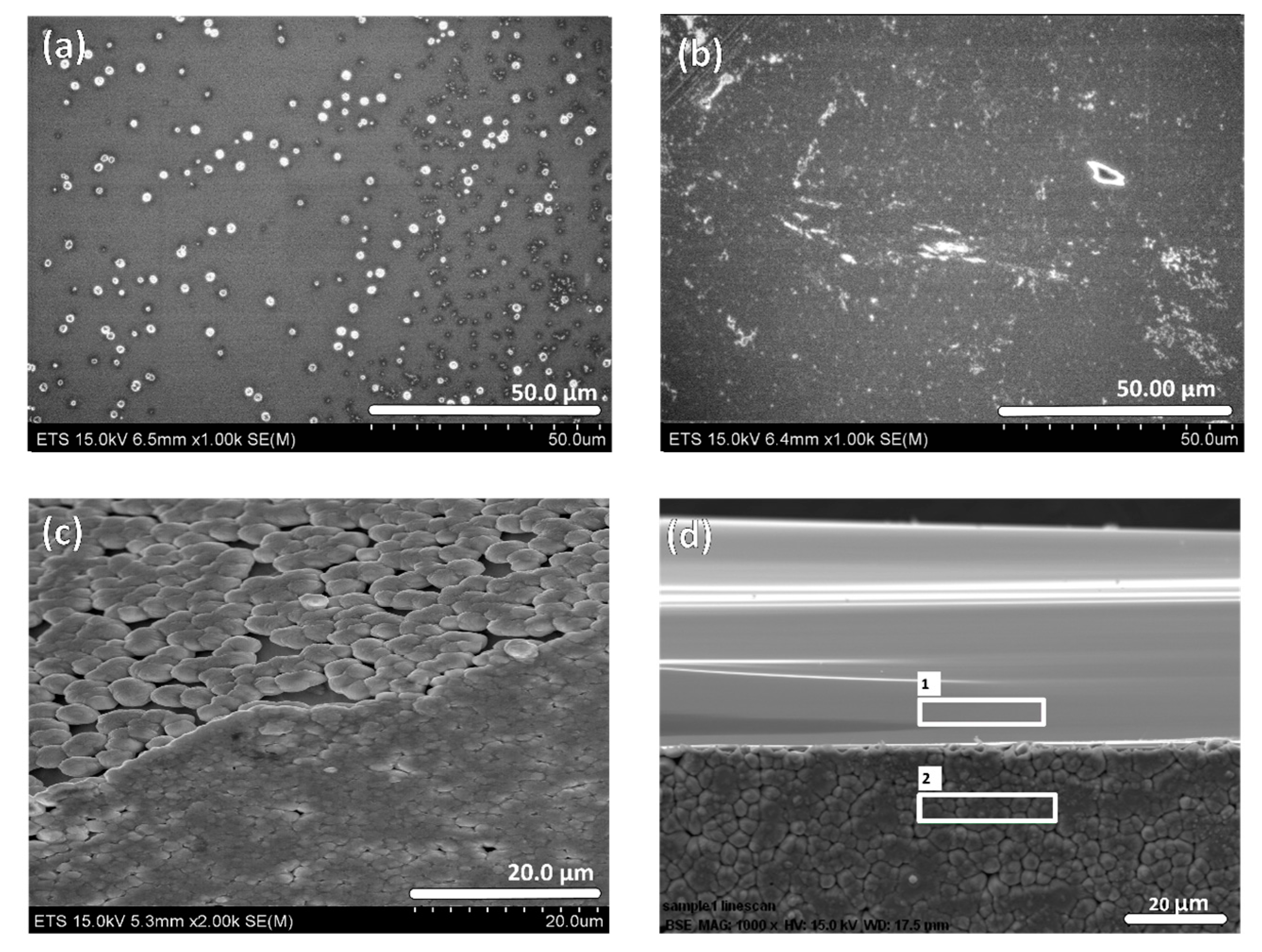
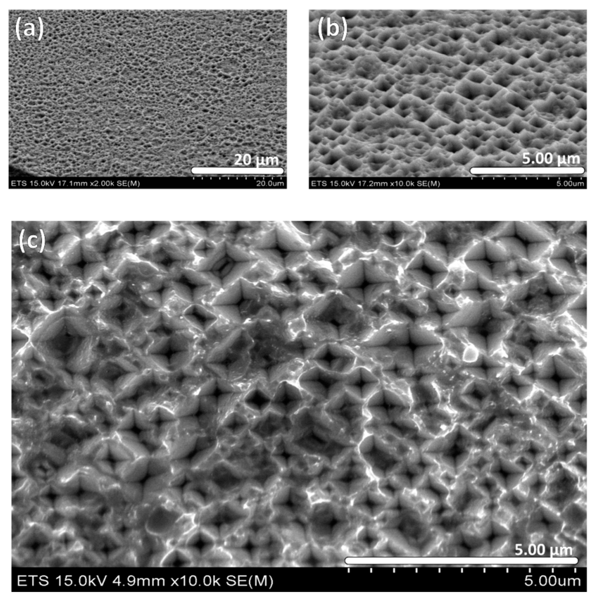
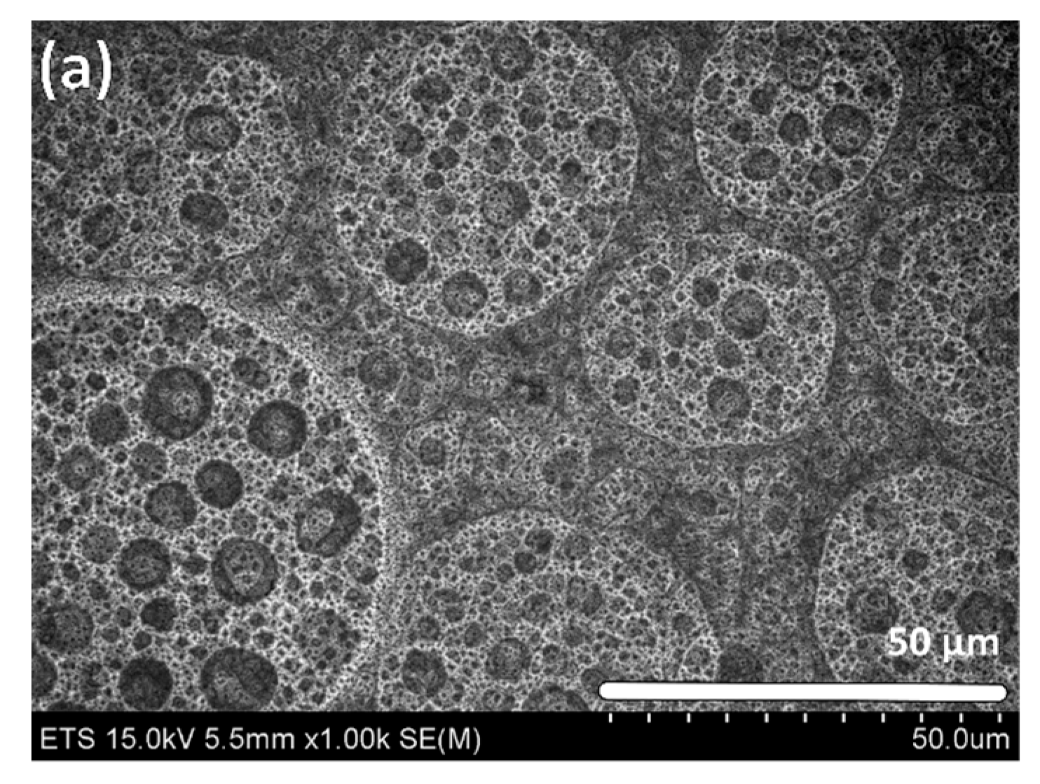
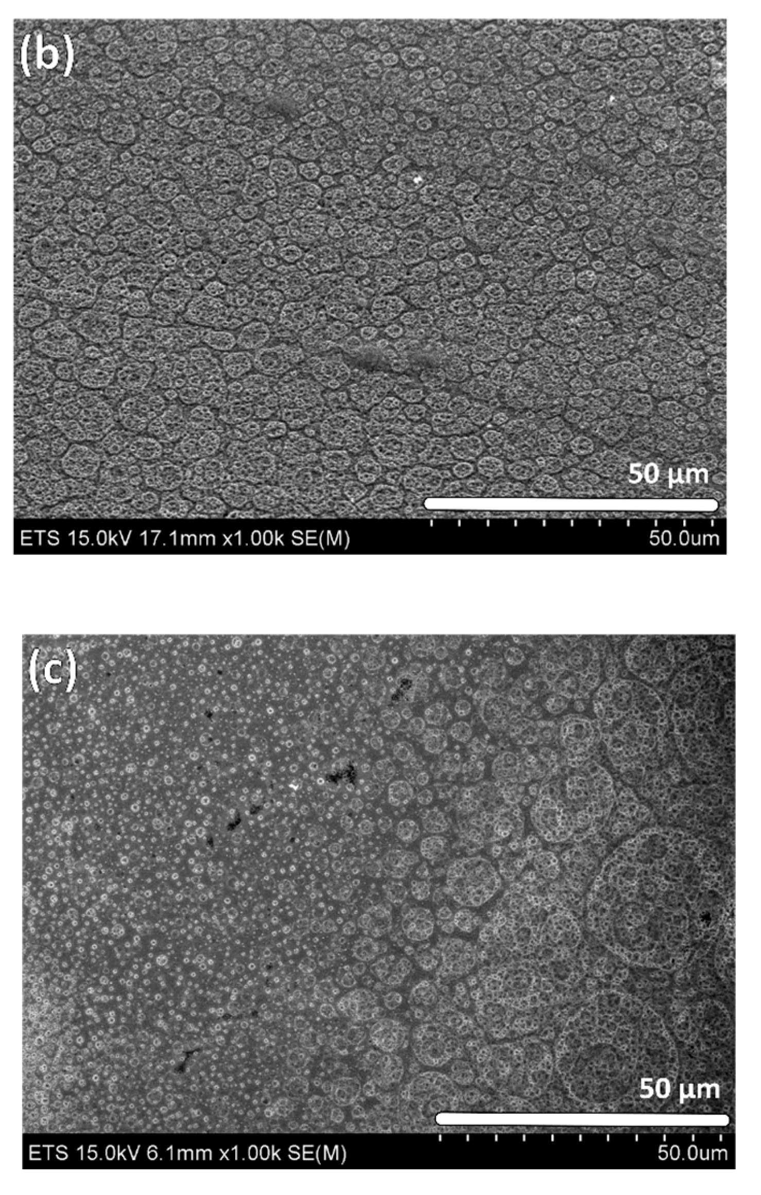
2.1. Structural Characterization by SEM
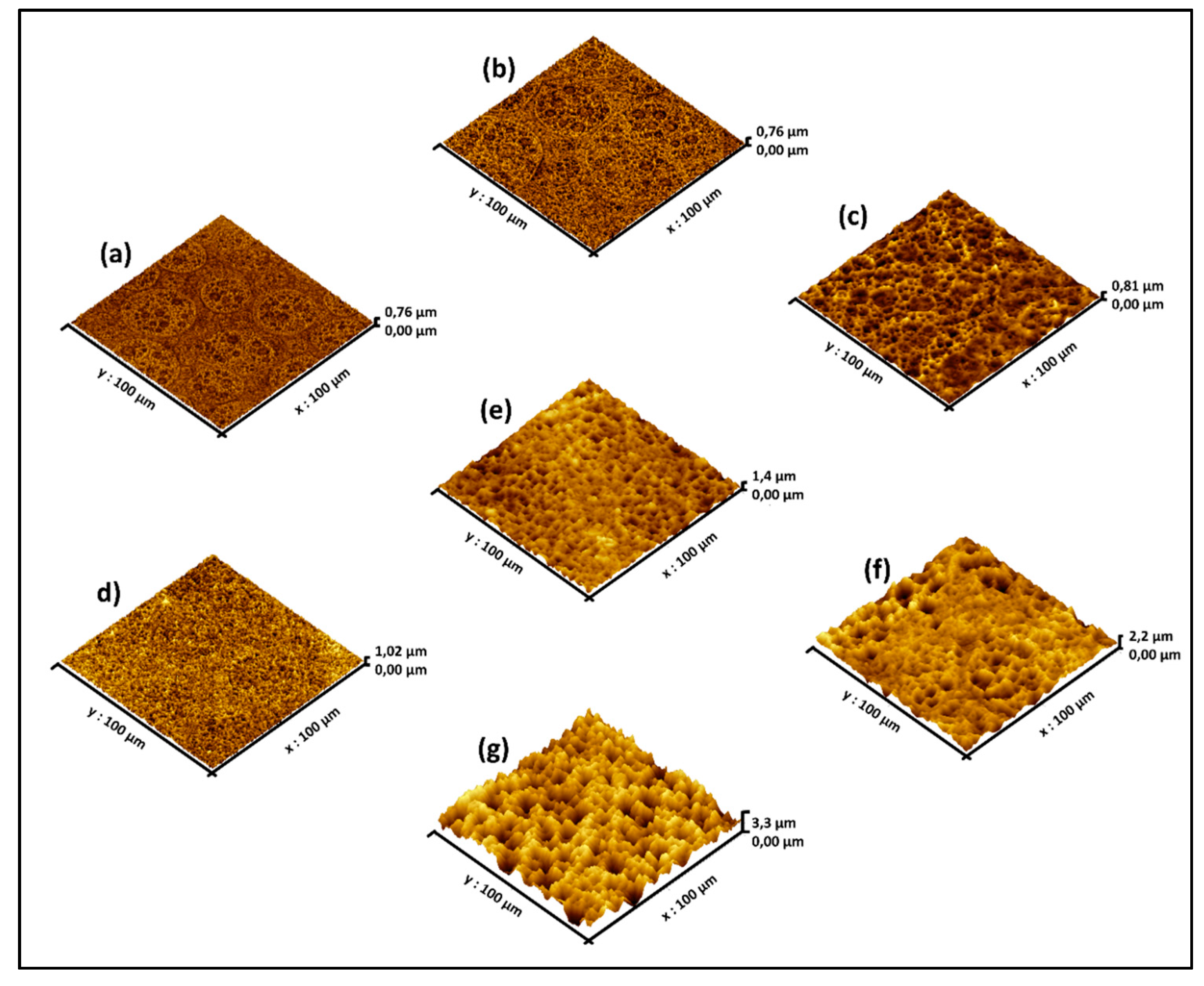
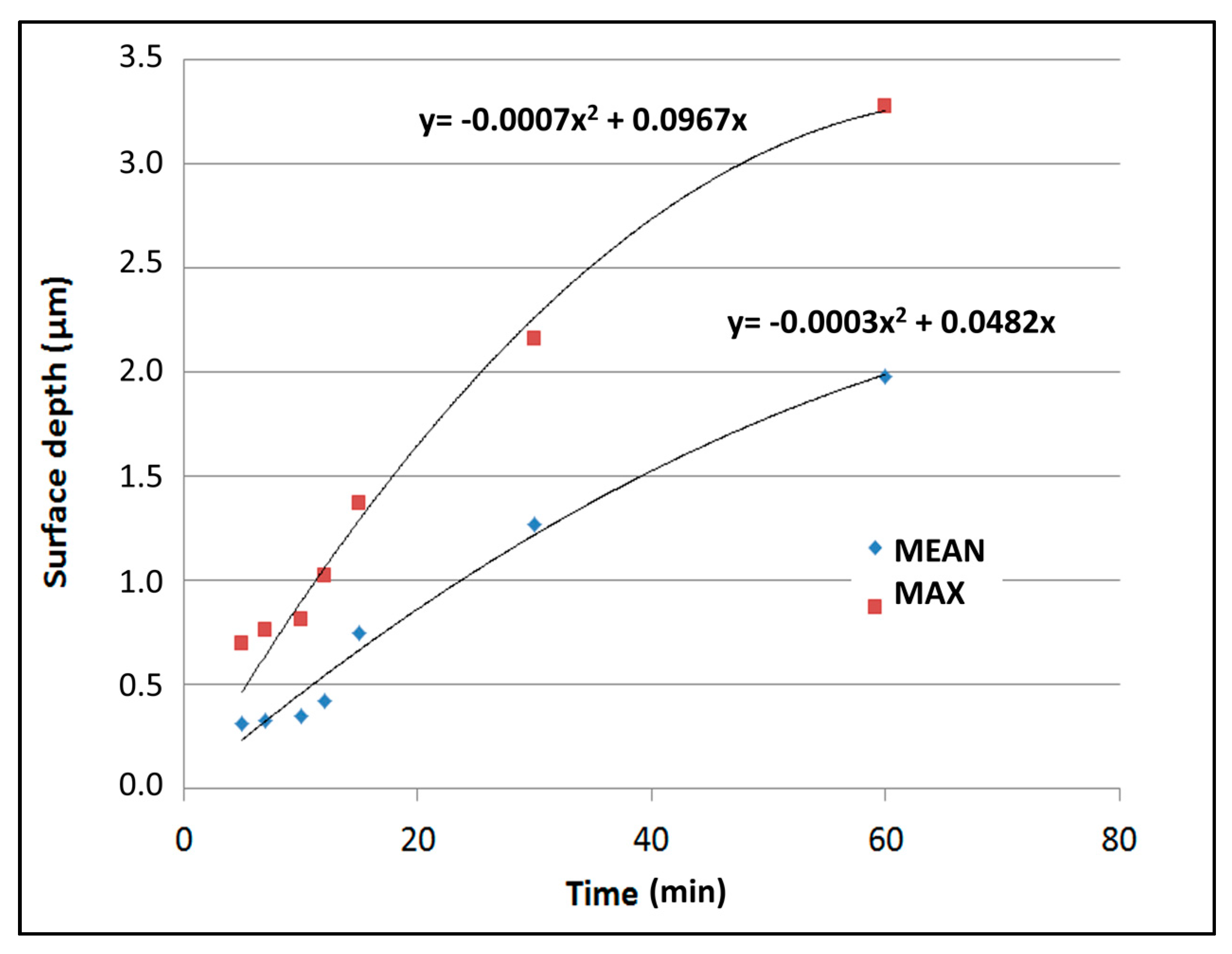
2.2. Surface Morphology Studied by AFM
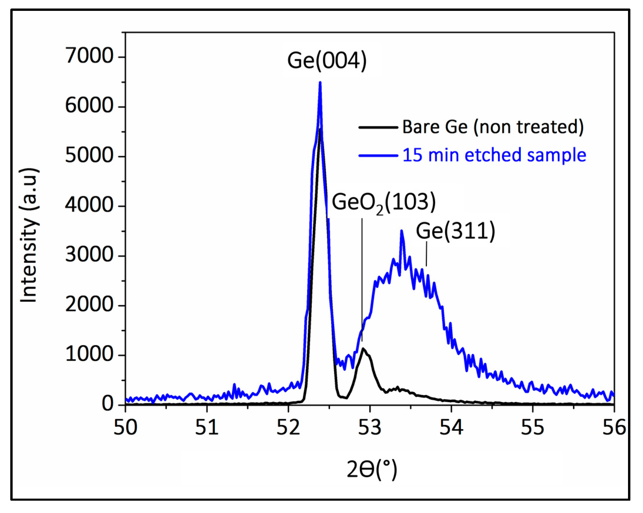
2.3. Structural Analysis Using X-ray Diffraction
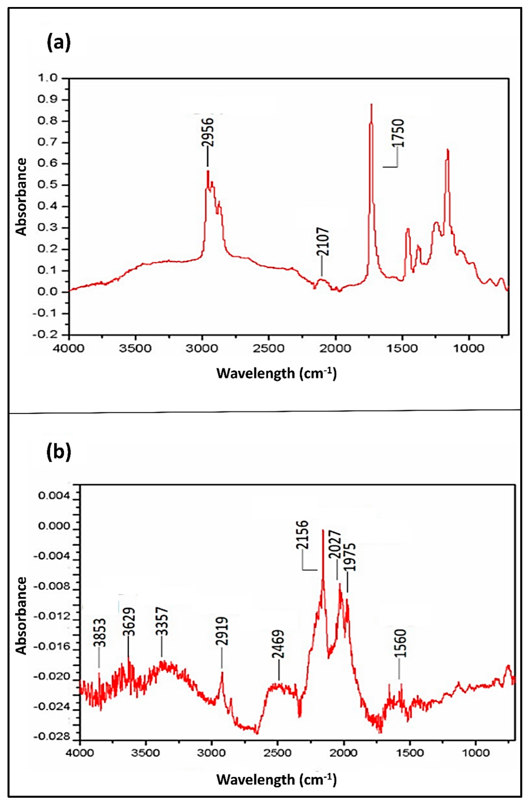
2.4. Surface Chemistry Analysis Using FTIR Analysis
2.5. Deeper Understand of the Surface Chemistry Using XPS Analysis
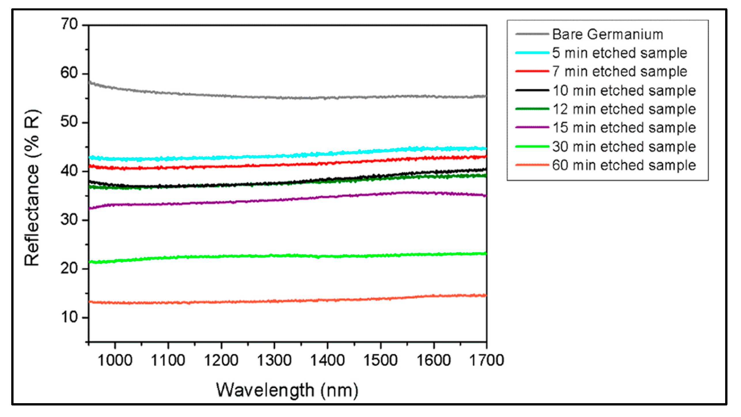
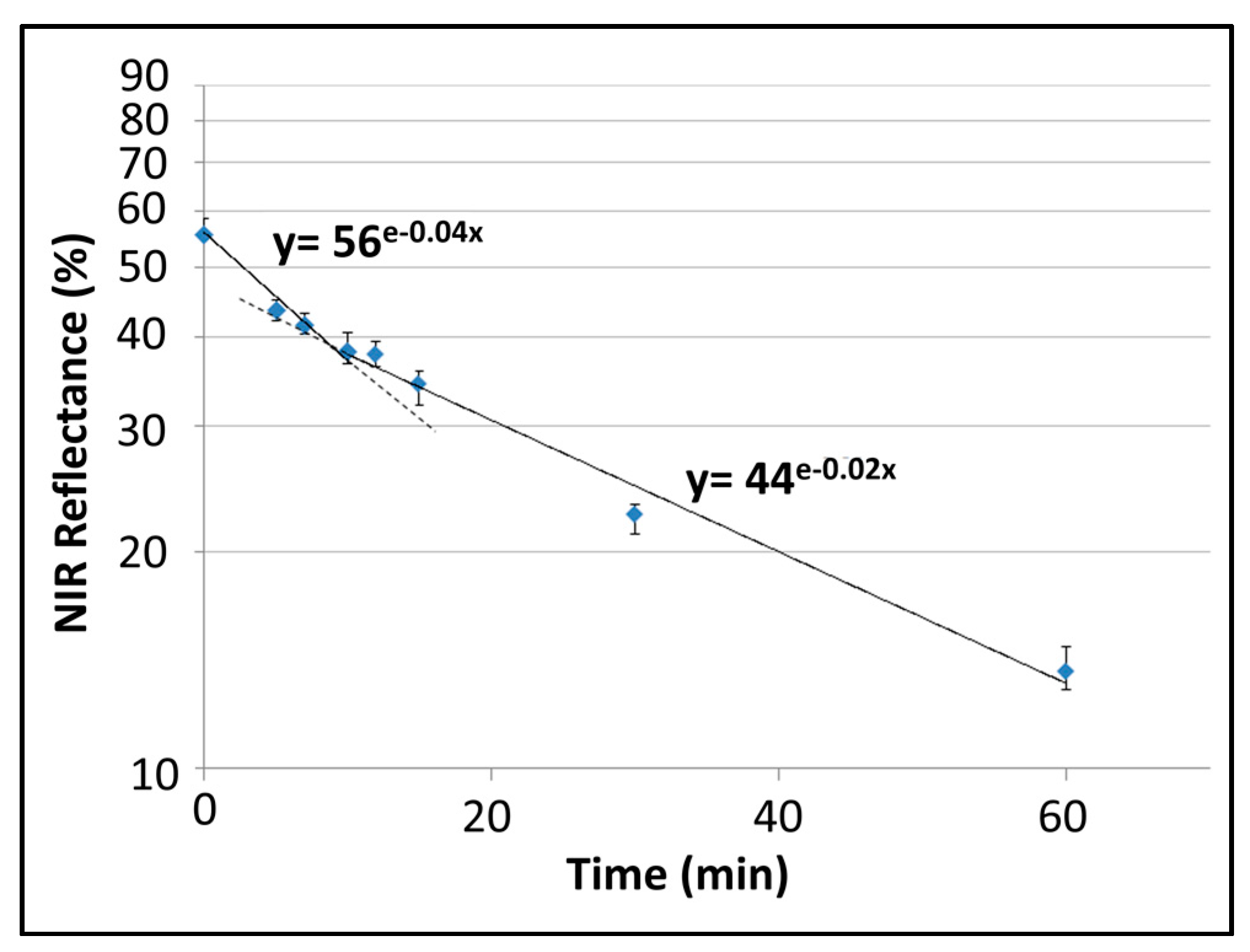
2.6. Broadband Reflectivity Measurements
3. Materials and Methods
4. Conclusions
Acknowledgments
Author Contributions
Conflicts of Interest
References
- Reinhardt, K.A.; Reidy, R.F. Handbook for Cleaning for Semiconductor Manufacturing: Fundamentals and Applications; John Wiley & Sons: Hoboken, NJ, USA, 2011; Volume 67. [Google Scholar]
- Loscutoff, P.W.; Bent, S.F. Reactivity of the germanium surface: Chemical passivation and functionalization. Ann. Rev. Phys. Chem. 2006, 57, 467–495. [Google Scholar] [CrossRef] [PubMed]
- Ramana, C.; Carbajal-Franco, G.; Vemuri, R.; Troitskaia, I.; Gromilov, S.; Atuchin, V. Optical properties and thermal stability of germanium oxide (GeO2) nanocrystals with α-quartz structure. Mater. Sci. Eng. B 2010, 174, 279–284. [Google Scholar] [CrossRef]
- Terakado, N.; Tanaka, K. Photo-induced phenomena in sputtered GeO2 films. J. J. Non-Cryst. Solids 2005, 351, 54–60. [Google Scholar] [CrossRef]
- Jiang, Z.; Xie, T.; Wang, G.; Yuan, X.; Ye, C.; Cai, W.; Meng, G.; Li, G.; Zhang, L. GeO2 nanotubes and nanorods synthesized by vapor phase reactions. Mater. Lett. 2005, 59, 416–419. [Google Scholar] [CrossRef]
- Su, Y.; Liang, X.; Li, S.; Chen, Y.; Zhou, Q.; Yin, S.; Meng, X.; Kong, M. Self-catalytic VLS growth and optical properties of single-crystalline GeO2 nanowire arrays. Mater. Lett. 2008, 62, 1010–1013. [Google Scholar] [CrossRef]
- Chen, X.; Cai, Q.; Zhang, J.; Chen, Z.; Wang, W.; Wu, Z.; Wu, Z. Synthesis and growth of germanium oxide nanoparticles in AOT reversed micelle. Mater. Lett. 2007, 61, 535–537. [Google Scholar] [CrossRef]
- Kim, H.W.; Shim, S.H.; Lee, J.W. Cone-shaped structures of GeO2 fabricated by a thermal evaporation process. Appl. Surf. Sci. 2007, 253, 7207–7210. [Google Scholar] [CrossRef]
- Poerschke, R.; Madelung, O. Data in Science and Technology, Semiconductors Group IV Elements and III–V Compounds; Springer: Berlin, Germany, 1991. [Google Scholar]
- Tsakalakos, L.; Balch, J.; Fronheiser, J.; Korevaar, B.; Sulima, O.; Rand, J. Silicon nanowire solar cells. Appl. Phys. Lett. 2007, 91, 233117. [Google Scholar] [CrossRef]
- Hu, L.; Chen, G. Analysis of optical absorption in silicon nanowire arrays for photovoltaic applications. Nano Lett. 2007, 7, 3249–3252. [Google Scholar] [CrossRef] [PubMed]
- Peng, K.Q.; Lee, S.T. Silicon nanowires for photovoltaic solar energy conversion. Adv. Mater. 2011, 23, 198–215. [Google Scholar] [CrossRef] [PubMed]
- Tsakalakos, L.; Balch, J.; Fronheiser, J.; Shih, M.-Y.; LeBoeuf, S.F.; Pietrzykowski, M.; Codella, P.J.; Korevaar, B.A.; Sulima, O.V.; Rand, J. Strong broadband optical absorption in silicon nanowire films. J. Nanophotonics 2007, 1, 013552. [Google Scholar] [CrossRef]
- Garnett, E.; Yang, P. Light trapping in silicon nanowire solar cells. Nano Lett. 2010, 10, 1082–1087. [Google Scholar] [CrossRef] [PubMed]
- Li, X. Metal assisted chemical etching for high aspect ratio nanostructures: A review of characteristics and applications in photovoltaics. Curr. Opin. Solid State Mater. Sci. 2012, 16, 71–81. [Google Scholar] [CrossRef]
- Qu, Y.; Liao, L.; Li, Y.; Zhang, H.; Huang, Y.; Duan, X. Electrically conductive and optically active porous silicon nanowires. Nano Lett. 2009, 9, 4539–4543. [Google Scholar] [CrossRef] [PubMed]
- Hung, Y.-J.; Lee, S.-L.; Wu, K.-C.; Tai, Y.; Pan, Y.-T. Antireflective silicon surface with vertical-aligned silicon nanowires realized by simple wet chemical etching processes. Opt. Express 2011, 19, 15792–15802. [Google Scholar] [CrossRef] [PubMed]
- Geyer, N.; Fuhrmann, B.; Huang, Z.; de Boor, J.; Leipner, H.S.; Werner, P. Model for the mass transport during metal-assisted chemical etching with contiguous metal films as catalysts. J. Phys. Chem. C 2012, 116, 13446–13451. [Google Scholar] [CrossRef]
- Peng, K.; Fang, H.; Hu, J.; Wu, Y.; Zhu, J.; Yan, Y.; Lee, S. Metal-Particle-Induced, Highly Localized Site-Specific Etching of Si and Formation of Single-Crystalline Si Nanowires in Aqueous Fluoride Solution. Chem. A Eur. J. 2006, 12, 7942–7947. [Google Scholar] [CrossRef] [PubMed]
- Fang, C.; Föll, H.; Carstensen, J. Electrochemical pore etching in germanium. J. Electroanal. Chem. 2006, 589, 259–288. [Google Scholar] [CrossRef]
- Garralaga Rojas, E.; Hensen, J.; Carstensen, J.; Föll, H.; Brendel, R. Porous germanium multilayers. Phys. Status Solidi C 2011, 8, 1731–1733. [Google Scholar] [CrossRef]
- Akkari, E.; Benachour, Z.; Aouida, S.; Touayar, O.; Bessais, B.; Benbrahim, J. Study and characterization of porous germanium for radiometric measurements. Phys. Status Solidi C 2009, 6, 1685–1688. [Google Scholar] [CrossRef]
- Rojas, E.G.; Terheiden, B.; Plagwitz, H.; Hensen, J.; Baur, C.; Strobl, G.F.; Brendel, R. Formation of mesoporous germanium double layers by electrochemical etching for layer transfer processes. Electrochem. Commun. 2010, 12, 231–233. [Google Scholar] [CrossRef]
- Rojas, E.G.; Hensen, J.; Baur, C.; Brendel, R. Sintering and reorganization of electrochemically etched mesoporous germanium layers in various atmospheres. Sol. Energy Mater. Sol. Cells 2011, 95, 292–295. [Google Scholar] [CrossRef]
- Marsella, J.; Durham, D.; Molnar, L. Handbook of Cleaning for Semiconductor Manufacturing; Scrivener Publishing LLC: Beverly, MA, USA, 2011. [Google Scholar]
- Adhikari, H.; Sun, S.; Pianetta, P.; Chidsey, C.E.; McIntyre, P.C. Surface Passivation of Germanium Nanowires; Stanford Linear Accelerator Center: Menlo Park, CA, USA, 2005. [Google Scholar]
- Bodlaki, D.; Yamamoto, H.; Waldeck, D.; Borguet, E. Ambient stability of chemically passivated germanium interfaces. Surf. Sci. 2003, 543, 63–74. [Google Scholar] [CrossRef]
- Souriau, L.; Terzieva, V.; Meuris, M.; Caymax, M. A Wet Etching Technique to Reveal Threading Dislocations in Thin Germanium Layers. Solid State Phenom. 2008, 134, 83–86. [Google Scholar] [CrossRef]
- Leancu, R.; Moldovan, N.; Csepregi, L.; Lang, W. Anisotropic etching of germanium. Sens. Actuators A Phys. 1995, 46, 35–37. [Google Scholar] [CrossRef]
- Jing, C.; Zhang, C.; Zang, X.; Zhou, W.; Bai, W.; Lin, T.; Chu, J. Fabrication and characteristics of porous germanium films. Sci. Technol. Adv. Mater. 2009, 10, 065001. [Google Scholar] [CrossRef] [PubMed]
- Sun, S.; Sun, Y.; Liu, Z.; Lee, D.-I.; Peterson, S.; Pianetta, P. Surface termination and roughness of Ge (100) cleaned by HF and HCl solutions. Appl. Phys. Lett. 2006, 88, 021903. [Google Scholar] [CrossRef]
- Schwartz, B.; Robbins, H. Chemical etching of germanium in solutions of HF, HNO3, H2O, and HC2H3O2. J. Electrochem. Soc. 1964, 111, 196–201. [Google Scholar] [CrossRef]
- Kern, W. Cleaning solutions based on hydrogen peroxide for use in silicon semiconductor technology. RCA Rev. 1970, 31, 187–206. [Google Scholar]
- Sioncke, S.; Brunco, D.P.; Meuris, M.; Uwamahoro, O.; Van Steenbergen, J.; Vrancken, E.; Heyns, M.M. Etch Rates of Ge, GaAs and InGaAs in Acids, Bases and Peroxide Based Mixtures. ECS Trans. 2008, 16, 451–460. [Google Scholar]
- Garralaga Rojas, E.J. Mesoporous Germanium Layer Formation by Electrochemical Etching. Ph.D. Thesis, Christian-Albrechts Universität Kiel, Kiel, Germany, 2010. [Google Scholar]
- Murray, P.R. Principles of Organic Chemistry: A Modern and Comprehensive Text for Schools and Colleges; Heinemann: Oxford, UK, 1977. [Google Scholar]
- Ballato, J.; Hawkins, T.; Foy, P.; Yazgan-Kokuoz, B.; Stolen, R.; McMillen, C.; Hon, N.; Jalali, B.; Rice, R. Glass-clad single-crystal germanium optical fiber. Opt. Express 2009, 17, 8029–8035. [Google Scholar] [CrossRef] [PubMed]
- Ko, C.-Y.; Lin, W.-T. SiO2-and CuO-enhanced growth of Ge–Si1−xGexOy and GeO2–Si1−xGexOy core–shell nanowires on a Si substrate via carbothermal reduction. Nanotechnology 2006, 17, 4464. [Google Scholar] [CrossRef]
- Jia, H.; Kloepsch, R.; He, X.; Badillo, J.P.; Winter, M.; Placke, T. One-step synthesis of novel mesoporous three-dimensional GeO 2 and its lithium storage properties. J. Mater. Chem. A 2014, 2, 17545–17550. [Google Scholar] [CrossRef]
- Chopra, K.; Major, S.; Pandya, D. Transparent conductors—A status review. Thin Solid Films 1983, 102, 1–46. [Google Scholar] [CrossRef]
- Robinson, J.T. Germanium Island Assembly on Metal-Patterned Silicon; ProQuest: Berkeley, CA, USA, 2007. [Google Scholar]
- Wedler, G. Introduction to the Properties of Crystal Surfaces. Z. Phys. Chem. 1975, 96, 175. [Google Scholar] [CrossRef]
- Patterson, A. The Scherrer formula for X-ray particle size determination. Phys. Rev. 1939, 56, 978. [Google Scholar] [CrossRef]
- Degallaix, S. Caractérisation Expérimentale des Matériaux; Presses Polytechniques et Universitaires Romandes: Lausanne, Switzerland, 2007. [Google Scholar]
- Stekolnikov, A.; Bechstedt, F. Shape of free and constrained group-IV crystallites: Influence of surface energies. Phys. Rev. B 2005, 72, 125326. [Google Scholar] [CrossRef]
- Pavia, L.D.; Lampman, G.M.; Kriz, G.S.; Vyvyan, J.R. Introduction to Spectroscopy, 5th ed.; CENGAGE Learning: Boston, MA, USA, 2013. [Google Scholar]
- Das, S.K.; Mahanta, S.P.; Bania, K.K. Oxidative coupling of 2-naphthol by zeolite-Y supported homo and heterometallic trinuclear acetate clusters. RSC Adv. 2014, 4, 51496–51509. [Google Scholar] [CrossRef]
- Kunst, S.R.; Beltrami, L.V.R.; Cardoso, H.R.P.; Santana, J.A.; Sarmento, V.H.V.; Müller, I.L.; Malfatti, C.D.F. Characterization of Siloxane-poly (methyl methacrylate) Hybrid Films Obtained on a Tinplate Substrate Modified by the Addition of Organic and Inorganic Acids. Mater. Res. 2015, 18, 151–163. [Google Scholar] [CrossRef]
- Choi, H.C.; Buriak, J.M. Preparation and functionalization of hydride terminated porous germanium Electronic supplementary information (ESI) available: FTIR thermal stability measurements and SEM images. Chem. Commun. 2000, 1669–1670. [Google Scholar] [CrossRef]
- Maroun, F.; Ozanam, F.; Chazalviel, J.-N. In-situ infrared monitoring of surface chemistry and free-carrier concentration correlated with voltammetry: Germanium, a model electrode. J. Phys. Chem. B 1999, 103, 5280–5288. Available online: http://www.rsc.org/suppdata/cc/b0/b004011h (accessed on 15 November 2015). [CrossRef]
- Arrais, A.; Benzi, P.; Bottizzo, E.; Demaria, C. Correlations among hydrogen bonding configuration, structural order and optical coefficients in hydrogenated amorphous germanium obtained by X-ray-activated chemical vapour deposition. J. Phys. D Appl. Phys. 2009, 42, 105406. [Google Scholar] [CrossRef]
- Abo-Ghazala, M.; Hazrny, S.A. Hydrogen bonding in hydrogenated amorphous germanium. Tsinghua Sci. Technol. 2004, 9, 177–180. [Google Scholar]
- Sunatkari, A.; Talwatkar, S.; Tamgadge, Y.; Muley, G. Synthesis, Characterization and Optical Properties of L-Arginine Stabilized Gold Nanocolloids. Nanosci. Nanotechnol. 2015, 5, 30–35. [Google Scholar]
- Maeng, J.Y.; Lee, J.Y.; Cho, Y.E.; Kim, S.; Jo, S.K. Surface dihydrides on Ge (100): A scanning tunneling microscopy study. J. Abbr. 2002, 81, 3555. [Google Scholar] [CrossRef]
- Tice, J.B. Synthesis and Fundamental Studies of Novel Main Group IV and Azidoarsenic CVD Precursors. Ph.D. Thesis, Arizona State University, Tempe, AZ, USA, 2008. [Google Scholar]
- Rivillon, S.; Chabal, Y.J.; Amy, F.; Kahn, A. Hydrogen passivation of germanium (100) surface using wet chemical preparation. Appl. Phys. Lett. 2005, 87, 253101. [Google Scholar] [CrossRef]
- Amy, S.R.; Chabal, Y.J.; Amy, F.; Kahn, A.; Krugg, C.; Kirsch, P. Wet Chemical Cleaning of Germanium Surfaces for Growth of High-k Dielectrics. Proceedings of MRS Proceedings, San Francisco, CA, USA, 1 December 2006; Volume 917. [Google Scholar] [CrossRef]
- Adhikari, H.; McIntyre, P.C.; Sun, S.; Pianetta, P.; Chidsey, C.E. Photoemission studies of passivation of germanium nanowires. Appl. Phys. Lett. 2005, 87, 263109. [Google Scholar] [CrossRef]
- Lu, Z. Air-stable Cl-terminated Ge (111). Appl. Phys. Lett. 1996, 68, 520–522. [Google Scholar] [CrossRef]
- Lu, Z.; Tyliszczak, T.; Hitchcock, A.; Dharma-Wardana, M. Structure of the Cl-passivated Ge (111) surface determined using X-ray absorption and first principles calculations. Surf. Sci. 1999, 442, L948–L952. [Google Scholar] [CrossRef]


| Mass Percent (%) | |||
|---|---|---|---|
| Sections | C | O | Ge |
| Section 1 | 1.95 | – | 98.05 |
| Section 2 | – | 22.90 | 77.10 |
| Sample | Immersion Time (min) | Mean Height (µm) | Maximum Height (µm) | Roughness (µm) |
|---|---|---|---|---|
| (a) | 5 | 0.31 | 0.70 | 0.06 |
| (b) | 7 | 0.33 | 0.76 | 0.06 |
| (c) | 10 | 0.35 | 0.81 | 0.07 |
| (d) | 12 | 0.42 | 1.02 | 0.07 |
| (e) | 15 | 0.75 | 1.37 | 0.13 |
| (f) | 30 | 1.27 | 2.16 | 0.19 |
| (g) | 60 | 1.98 | 3.28 | 0.40 |
| Valence Vibration Frequency (cm−1) | Attribution of Peaks to Atomic Bands | References |
|---|---|---|
| 1560 | N–H | [46] |
| 1750 | C=O | [46,47,48] |
| 1975 | Ge–Hx (x = 1) or X=C=Y (X,Y) | [25,46,49,50,51,52] |
| 2027 | Ge–Hx (x = 2) or X=C=Y | [25,46,49,51] |
| 2107 | C≡C | [46] |
| 2156 | Ge–Hx (x = 3), X=C=Y or C≡C | [25,46,51] |
| 2469 | O–H | [46] |
| 2919 | C–H | [46,48] |
| 2956 | C–H | [46,48,49] |
| 3357 | N–H, O–H (H bonded) or O–H (carboxylic) | [46,48] |
| 3629 | Free O–H or C–H | [46,48] |
| 3853 | O–H (stretching absorption of COOH) | [53] |
| Element | Binding Energy (eV) | Relative Atomic % | |||
|---|---|---|---|---|---|
| Measured with a MgKα Source | Measured with a AlKα Source | ||||
| Pristine | 15 min Etch | Pristine | 15 min Etch | ||
| Ge | 31.9 | 5.4 | 3.0 | 7.6 | 5.1 |
| C | 285.1 | 74.6 | 86.6 | 75.1 | 83.2 |
| O | 532.1 | 12.6 | 10.2 | 13.3 | 11.2 |
| F | 689.8 | 7.3 | – | 3.9 | – |
| Zn | 1021.7 | – | 0.2 | – | 0.4 |
| Element | Binding Energy (eV) | Full Width Half Maximum (FWHM) | Identification | Relative Atomic % | |
|---|---|---|---|---|---|
| Pristine | 15 min Etch | ||||
| Ge | 29.4 | 1.4 | Ge0 | 2.3 | 2.4 |
| 30.2 | 2.0 | Ge1+ (Ge–H or GexOy, x = 2, y = 1) | – | 0.4 | |
| 32.2 | Ge3+(GexOy, x = 2, y = 3) | – | 0.5 | ||
| 33.0 | Ge4+ (GeO2) | 3.3 | – | ||
| C | 285.0 | 1.3 | C–C | 80.7 | 81.8 |
| 286.8 | 1.6 | C–O | – | 4.6 | |
| O | 531.3 | 2.2 | Ge–O, Ge–OH (hydroxyl in surface) | – | 6.5 |
| 532.0 | 13.7 | – | |||
| 532.8 | C–O | – | 3.8 | ||
© 2017 by the authors. Licensee MDPI, Basel, Switzerland. This article is an open access article distributed under the terms and conditions of the Creative Commons Attribution (CC BY) license (http://creativecommons.org/licenses/by/4.0/).
Share and Cite
Chaabane, I.; Banerjee, D.; Touayar, O.; Cloutier, S.G. Shallow V-Shape Nanostructured Pit Arrays in Germanium Using Aqua Regia Electroless Chemical Etching. Materials 2017, 10, 854. https://doi.org/10.3390/ma10080854
Chaabane I, Banerjee D, Touayar O, Cloutier SG. Shallow V-Shape Nanostructured Pit Arrays in Germanium Using Aqua Regia Electroless Chemical Etching. Materials. 2017; 10(8):854. https://doi.org/10.3390/ma10080854
Chicago/Turabian StyleChaabane, Ibtihel, Debika Banerjee, Oualid Touayar, and Sylvain G. Cloutier. 2017. "Shallow V-Shape Nanostructured Pit Arrays in Germanium Using Aqua Regia Electroless Chemical Etching" Materials 10, no. 8: 854. https://doi.org/10.3390/ma10080854
APA StyleChaabane, I., Banerjee, D., Touayar, O., & Cloutier, S. G. (2017). Shallow V-Shape Nanostructured Pit Arrays in Germanium Using Aqua Regia Electroless Chemical Etching. Materials, 10(8), 854. https://doi.org/10.3390/ma10080854