Article

The Choice of the Control in the Single-Phase Voltage Source Inverters for UPS Systems

by
Zbigniew Rymarski
Department of Electronics, Electrical Engineering and Microelectronics, Faculty of Automatic Control, Electronics and Computer Science, Silesian University of Technology, 44-100 Gliwice, Poland
Energies 2026, 19(6), 1548; https://doi.org/10.3390/en19061548
Submission received: 24 February 2026 / Revised: 7 March 2026 / Accepted: 16 March 2026 / Published: 20 March 2026
(This article belongs to the Special Issue Power Systems: Stability Analysis and Control)

Abstract

The paper presents four solutions to the voltage source inverter (VSI) control system with existing delays in the measurement channels and the middle switching frequency (25,600 Hz): Single-Input Single-Output Coefficient Diagram Method (SISO-CDM), Multi-Input Multi-Output Passivity-Based Control (MISO-PBC), Multi-Input Multi-Output One-Sample-Ahead Preview Controller (MISO-OSAP), and MISO-OSAP with Luenberger Observer (MISO-OSAP-LO). The theory, including adjustments to controller gains or to the coefficients of the characteristic equation of the closed-loop system, is presented. Simulations of the VSI operation with these control systems for the nonlinear load and the dynamic resistive load (per the requirements of the EN 62040-3 standard) are presented. The SISO-CDM and MISO-PBC are finally selected for experimental verification of the simulations. The results of the tests enable the selection of the control type for a particular VSI design based on its cost and an estimation of the advantages of the more expensive solution. The paper should help in engineering design according to the remarks in the paper.

1. Introduction

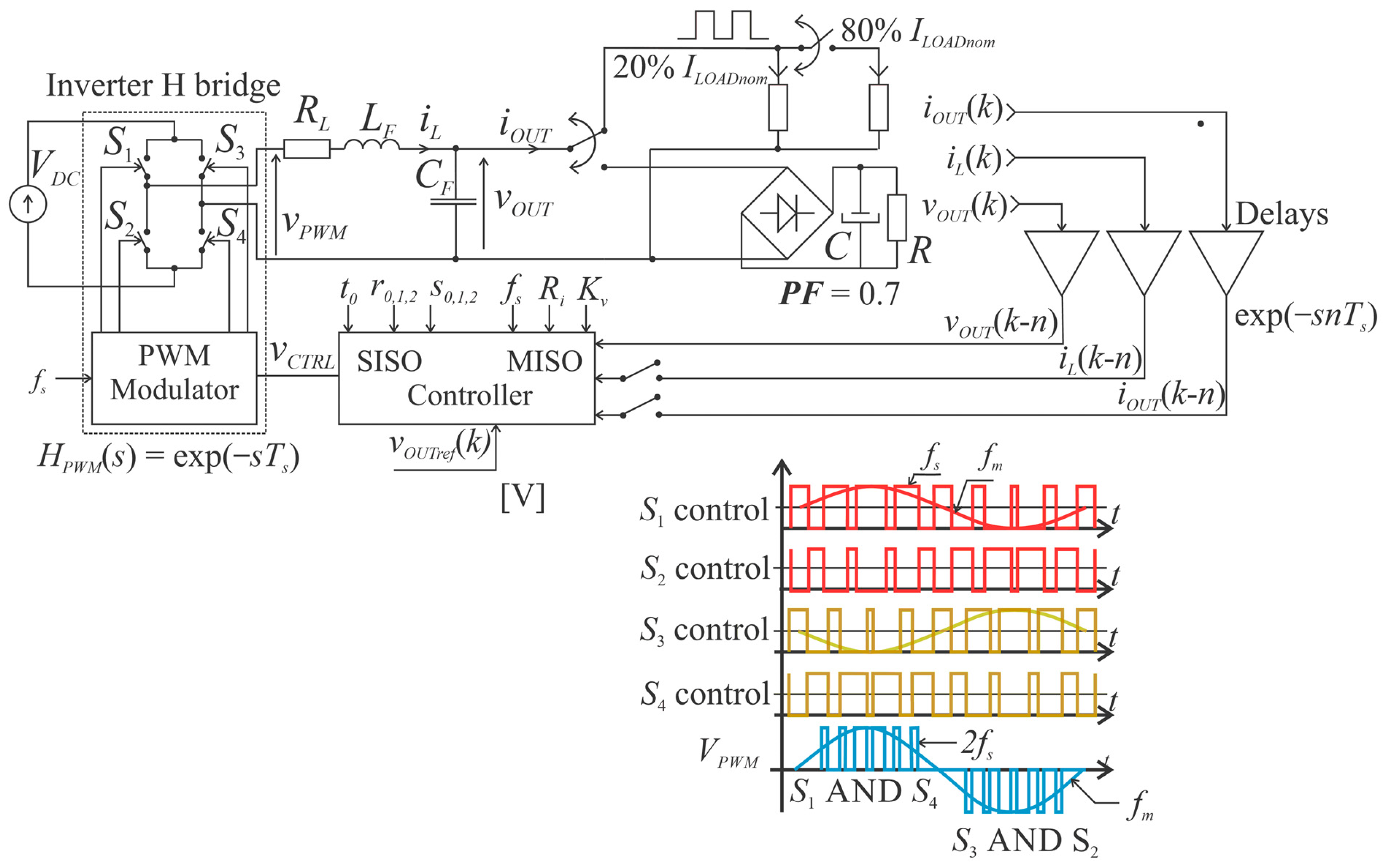
There is a variety of instantaneous control systems for the stand-alone VSI. The first difference between them is in the number of input variables of the controller. The simplest and cheapest are Single-Input Single-Output (SISO) systems, when only the output voltage is measured and controlled. In this case, the most common approach is to treat the output voltage as the independent disturbance [1,2,3,4,5,6]. For the low frequency band, below the corner frequency of the output filter, the influence of the output current on the output voltage, that is equal to the negative product of the current and the output VSI impedance for the open feedback loop, is divided by the gain of the controller, which is high in this frequency range [7]. One of the easiest to design SISO control algorithms is the Coefficient Diagram Method (CDM) [8,9,10] when the controller is designed in such a way that the coefficients of the characteristic equation of the closed loop system are equal to the coefficients of the reference characteristic equation based on the Standard Manabe Form. In the case of the VSI with a second order of the nominator and denominator of the controller, this kind of SISO controller can be treated as a PID controller with Manabe coefficients. It generally works well in accordance with the requirements of the IEC 62040-3 standard [11]. For the UPS system with the power below 3 kW, the nonlinear rectifier RC load with a Power Factor of 0.7 is basic. The dynamic load is defined as a step load change from 20% to 100% and 100% to 20% of the nominal load at the point of the maximum of the output sinusoidal voltage (Figure 1). More demanding is the step decrease because the current flowing through the filter coil is redirected to the output capacitor, causing the voltage overshoot (the feedback is always delayed at least by one switching period, Ts).
In the Multi-Input Single-Output (MISO) control systems, the VSI output voltage, current, and the inductor current are treated as the state variables, which are measured and implemented in the control law. Measuring the output current, we omit the problem with the hidden loop from the output voltage to the output current. The first considered MISO control is the Passivity-Based Control (PBC) [3,12,13,14,15,16,17,18]. The idea of PBC (similar to the Lyapunov approach [12]) is based on the statement that the energy stored in the VSI system should be lower than the energy delivered to the system. However, the system directly taking into account voltage and currents could be faster. The last, initially considered control MISO system is deadbeat control [19,20,21]. It is pure discrete, the fastest control that shifts the roots of the characteristic equation of the closed-loop system to zero in the z-plane. It is the only system where we can predict that the controlled output variable (in our case, the VSI output voltage) will reach the reference value after a countable number of switching periods. In the case of the VSI, it can be assigned to the next switching period. The One-Sample-Ahead Preview Control (OSAP) [19,20,21] is a kind of deadbeat control. A. Kawamura [19] showed that assuming vOUT(k + 1) = vref(k + 1) leads to a deadbeat control law that is simply created from one of the discrete state space equations. The deadbeat control law has no assigned gains for the voltage or current. Deadbeat control is very sensitive to delays in the system. The common problem for all these controllers is a delay in the measurement channels and the PWM modulator [22]. It can be seen that one of the ways of using it in a real system with delays is by implementing the prediction of the state variables. The delay in the PWM modulator is a result of storing data in one switching period and changing pulse width according to the stored data in the next period. The modulator delay is equal to one switching period. All the measurement channels are a kind of low-pass filter. In the frequency range below the resonant frequency of the output filter, it is possible to model them as a simple delay equal to some switching periods. In our experimental VSI, we use switching frequencies fs equal to 12,800, 25,600, or 51,200 Hz. It was shown in [22] that for the low fs = 12,800 Hz, the delays are so serious that the necessary solution for control with a delay can be the prediction of the state variables. For fs equal to 25,600 Hz, the delays have a small but visible influence on control, and for fs = 51,200 Hz, they are unnoticeable. The so-called first schema of PWM was described many years ago in [23] and presented further in [24] and many others. In this scheme, the bridge transistors are switched with frequency fs, but the magnetizing current of the filter coil has a double 2fs frequency. So, the reasonable switching frequency, without excessive power losses in the filter coil core, was chosen as fs = 25,600 Hz.
The goal of the paper is to show that different types of control can be useful for different requirements of the VSI designer. The CDM control is cheap (it has only one output voltage measurement channel) and quite fast. The MISO-PBC is based on energy calculation, so in the real device, it is not so good for fast load changes, but perfect for the harmonic distortions and the steady state. The MISO-OSAP is very fast, the best for fast load changes, but not so good in the steady state, and not robust to delays. After the theoretical presentations of control laws for all these controls, the simulations and the experimental verification (for the chosen controls) will be shown. We cannot forget about the other solutions—e.g., the double-loop SISO with the plug-in Repetitive Controller (RC), a kind of harmonics generator in the outer loop [24,25], perfectly dumping only harmonics distortions and steady-state error. But they implement other problems (e.g., RC remembers disturbance from the previous fundamental period even if it vanishes). The chosen four controls should clearly show differences between SISO and MISO, based on the energy calculation, and a fast pure discrete MISO control.

2. Basic Assignments and Calculations for the VSI Simulation

First, we should have the basic parameters of the simulated system. The output filter was initially calculated for the steady state. So LFCF was calculated to keep the output voltage maximum harmonic below 3% (1) and to keep THD below 5% (IEEE 519 [26] for low voltages) or below 8% (IEC 62040-3 [11] for UPS system). The maximum harmonic value is for the PWM duty ratio τ = 0.5.
( h m a x τ = 0.5 / h 1 ) O U T < 3 %
The highest harmonic is equal to or close (±50 Hz) to the double switching frequency 2fs (2) for the first PWM scheme [24] and three-level modulation.
L F C F = 1 ( 2 f s ) 2
In [27], a cost function F (3) was created as the sum of the absolute values of the reactive powers in the filter inductor and capacitor, approximately only for the fundamental harmonic h1. Having the minimum induction LF as a function of the capacitance CF, there is a possibility to calculate the induction value LF for which the cost function has a minimum (4).
F ω m ( L F I L F h 1 r m s 2 + 1 L F ( 2 f s ) 2 V O U T h 1 r m s 2 )
We assume that ILFh1rmsIOUTh1rms and fs >> fm.
F L F ω m ( I O U T h 1 r m s 2 1 ( L F 2 f s ) 2 V O U T h 1 r m s 2 ) = 0
From (2) and (4), we can obtain the particular values of LF (5) and CF (6).
L F = 1 2 f s R L O A D
C F = 1 2 f s 1 R L O A D
For fs = 25,600 Hz, VOUTh1rms/IOUTh1rms = RLOAD = 50 Ω, LF ≈ 1 mH, CF ≈ 0.4 µF. However, the PWM modulator introduces a delay equal to the switching period, and the control cannot do anything during this period. We can assume that it will be a constant current forced by the filter coil during one switching period (the period Ts of bridge control, not the period Ts/2 of the filter inductor current). So, for the 5 A step load current decrease ΔiOUT = 5 A, Ts = 1/fs = 39 µs, for assumed ΔvOUT = 5 V, CF = TsΔiOUTvOUT, CF = 39 µF. Finally, LF = 2 mH and CF = 51 µF were used in the simulation and the experimental model (CF—Metallized Polypropylene capacitor WIMA MKP 4). The other parameter is the serial equivalent resistance RL, the sum of all the serial resistances, the coil winding resistance, the equivalent resistance of the coil caused by the power losses in its core, and the serial resistance of two serially connected switched-on bridge transistors and all other VSI’s PCB and connectors’ resistances. This resistance is variable, depending on the load, but assuming RL = 1 Ω was reasonable for the coil core made of the alloy-powder high-quality material MS-Sendust [28] and the used bridge transistors Vishay Siliconix (2201 Laurelwood Road, Santa Clara, CA 95054, USA) MOSFET IRFP360LC. The LF and CF values were assumed constant, and the serial parasitic resistance of the MKP capacitor was neglected. For the nonlinear rectifier RC load, when the rectifier begins conducting current to the load capacitor in tRON time (it was simplified as ωmtRON = π/4, M is a modulation index, M ≤ 1), the maximum possible step voltage on the filter input is ∆vFIN = VDC(1 − Msin(ωmtRON)). So, we have to limit the maximum value LFmax of the filter inductor to the value that enables the rise in the inductor current controlled by feedback to follow the reference sinusoidal voltage in the inverter output in tRON time. The approximated value LFmax was calculated in [24] (7), where for the serial resistance of the rectifier Rs = 1, the worst-case M = 1, the LFmax < 2.6 mH. So, our chosen LF = 2 mH value is acceptable. The real value of M should be low enough (e.g., equal to 0.7, used further) to ensure the possibility of a rapid answer for the step load change in the maximum of the sinusoidal output waveform.
L F m a x < ( R L + R s ) 2 M 1 ω m
Figure 1 presents the block diagram of the simulated and tested VSI, the single-phase inverter with the three-level, double-edge PWM scheme, where the switching on periods of the modulating signals (PWM envelope) for each transistor from Figure 1 are described by (8)–(11) [23,24]. For k = 1 … (fs/fm):
S 1 : T O N ( k ) / T s = 0.5 M sin ( 2 π k f m / f s ) + 0.5
S 2 : N O T ( S 1 )
S 3 : T O N ( k ) / T s = 0.5 M sin ( ( 2 π k f m / f s ) + π ) + 0.5
S 4 : N O T ( S 3 )
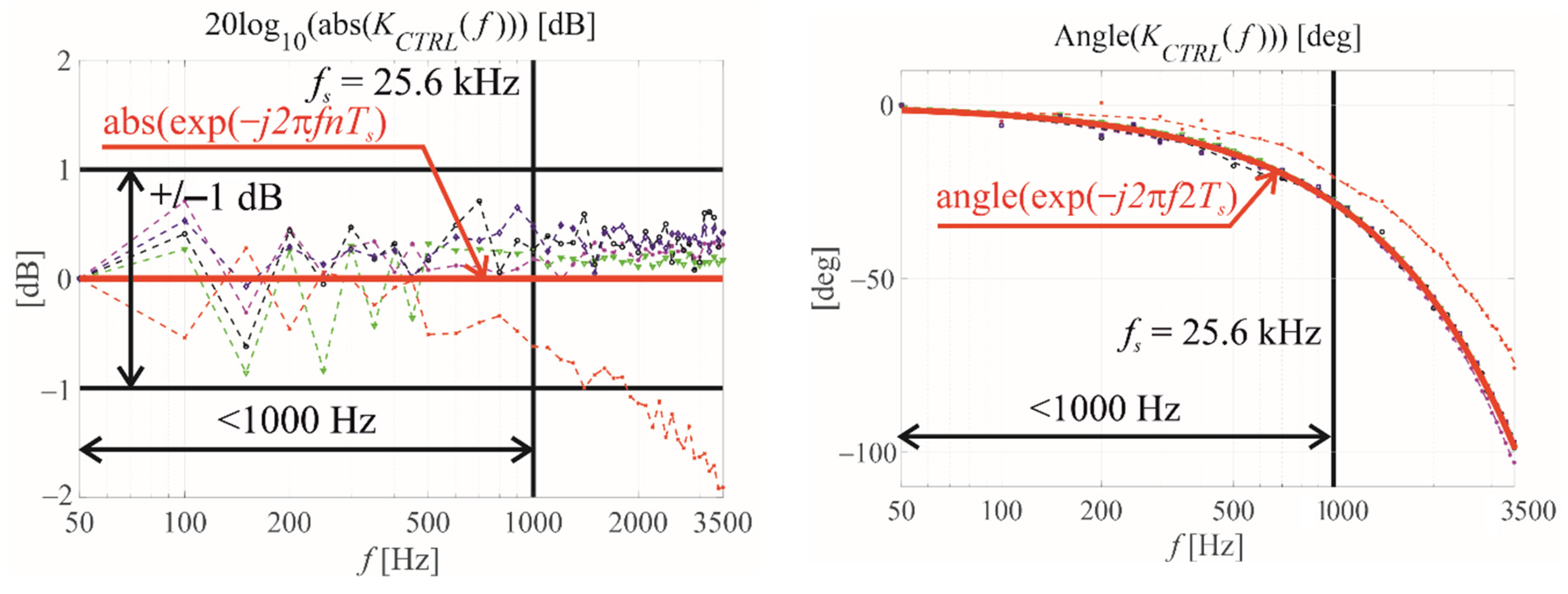
The way of measuring the Bode plots of the inverter and its measuring channels was previously widely described in [29]. The measurement of Bode plots of the output voltage channel is based on measuring the ratios of the test signal VChOUT(nfm) (summed with the fundamental signal) to the fundamental signal VChOUT(fm) at the output of the channel and VChIN(nfm) to VChIN(fm) at the input of the channel (12). The idea of creating test signals is based on creating harmonics nfm of the fundamental signal. The similar design (except for the channels input, where a differential amplifier is used in the voltage channel and transducers LA25-NP in the current channels) of all the measuring channels justifies the approximation (<1 kHz) that all channels have the same Bode plots in the low-pass frequency band.
K C h C T R L ( j 2 π n f m ) = V C h O U T n f m / V C h O U T f m V C h I N n f m / V C h I N f m e x p ( j a r g ( n f m ) )
Figure 2 presents the Bode plots of the five tested experimental VSIs (Figure 3). They are compared with the simple exponential function exp(−j2πfnTs). It can be seen that for the frequency range below the resonant frequency of the VSI output filter, f < 1 kHz, the simple delay can model the frequency-dependent characteristics of the channel quite accurately. The delay is nTs, where n is equal to two in the particular tested VSI at fs = 25,600 Hz. In the simulation, a Zero-Order Hold Unit simulates the analog-to-digital converter, and an additional delay of 2Ts simulates the delay of the measurement channel. But in a more developed measurement channel, there can be a higher delay [22].
The linearised discrete state-space equations are (13) and (14), where vCTRL is the input signal to the PWM modulator (Figure 1), and x(k) = [vOUT(k) iLF(k) iOUT(k)]T. They are based on the idea of solving the continuous state space equations in one switching period and the linear approximation of the exponential function exp(ATONk/2), where A is a state space matrix [19,24,30]. It should be noticed that the control system has fs switching frequency. However, the output filter input voltage at frequency 2fs, which is a result of the coincidence of the two shifted pulses generated with the fs switching frequency, does not influence control. The presented discrete model (13)–(26) of the VSI plant enables the creation of the control law of VSI.
x ( k + 1 ) = A D x ( k ) + G D T O N ( k ) = A D x ( k ) + G D T s V D C v C T R L ( k )
y ( k + 1 ) = C D x ( k )
The state, input, and output matrices are (15).
A D = Φ T s = ϕ 11 ϕ 12 ϕ 13 ϕ 21 ϕ 22 ϕ 23 ϕ 31 ϕ 32 ϕ 33 ,   G D = g 11 g 21 g 31 ,   C D = C = [ 1 0 0 ]
For the three-level double-edge modulation, coefficients of the state matrix are (16)–(23):
ξ F = 1 2 R L C F L F ,   ω F 0 = 1 C F L F ,   E A = exp ( ξ F ω F 0 T s ) ,   E G = s q r t ( ξ F ω F 0 T s / 2 )
φ 11 = [ cos ω F 0 T s + ξ F sin ω F 0 T s ] E A ,
φ 12 = 1 ω F 0 C F sin ( ω F 0 T s ) E A ,
φ 13 = 1 ω F 0 C F sin ( ω F 0 T s ) E A + R L ( φ 11 1 ) ,
φ 21 = 1 ω F 0 L F sin ( ω F 0 T s ) E A ,
φ 22 = [ cos ( ω F 0 T s ) ξ F sin ( ω F 0 T s ) ] E A ,
φ 23 = 1 [ cos ω F 0 T s + ξ F sin ω F 0 T s ] E A ,
φ 31 = 0 ,   ϕ 32 = 0 ,   φ 33 = 1
Coefficients of the input matrix are (24)–(26):
g 11 = V D C ω F 0 sin ( ω F 0 T s / 2 ) E G ,
g 21 = V D C L F [ cos ( ω F 0 T s / 2 ) ξ F sin ( ω F 0 T s / 2 ) ] E G ,
g 31 = 0
The control of the VSI’s output voltage for the open loop and three-level, double-edge modulation is (27). It was shown in [24] that double-edge modulation introduces additional delay because the interval between two consecutive pulses (k) and (k − 1) depends on the previous (k − 1) pulse width. The PWM modulator introduces an additional delay. Ginv in (27) is the inverter transfer function of the TON to VOUT.
V O U T z = z 1 T s V D C G i n v V C T R L z Z O U I z I O U T z
The inverter transfer function of VCTRL to VOUT, including the delay of the PWM modulator and the delay of the double-edge algorithm, is (28), presented further as (29) with coefficients (30). What is important for further calculations, the VDC value in Equations (28) and (29) simplifies with the VDC value in gi coefficients (24)–(26). So, (28) and (29) are not finally dependent on VDC.
K V S I = V O U T ( z ) V C T R L ( z ) = z 1 T s V D C G i n v = N ( z 1 ) D ( z 1 ) = T s V D C g 11 z 2 + T s V D C ( φ 12 g 21 φ 22 g 11 ) z 3 1 ( φ 11 + φ 22 ) z 1 + ( φ 11 φ 22 φ 12 φ 21 ) z 2
K V S I = N ( z 1 ) D ( z 1 ) = a 2 z 2 + a 3 z 3 1 + b 1 z 1 + b 2 z 2
where
a 2 = T s V D C g 11 z 2 ,   a 3 = T s V D C ( φ 12 g 21 φ 22 g 11 ) z 3 ,   b 1 = ( φ 11 + φ 22 ) ,   b 2 = ( φ 11 φ 22 φ 12 φ 21 )

3. SISO CDM Control

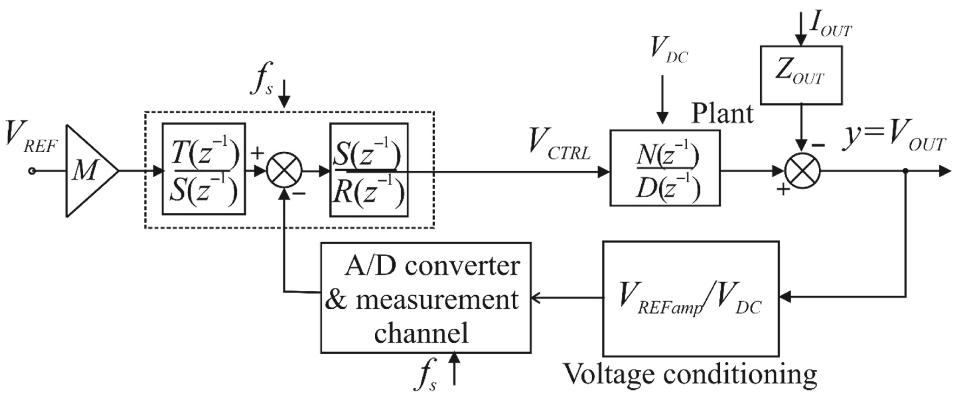
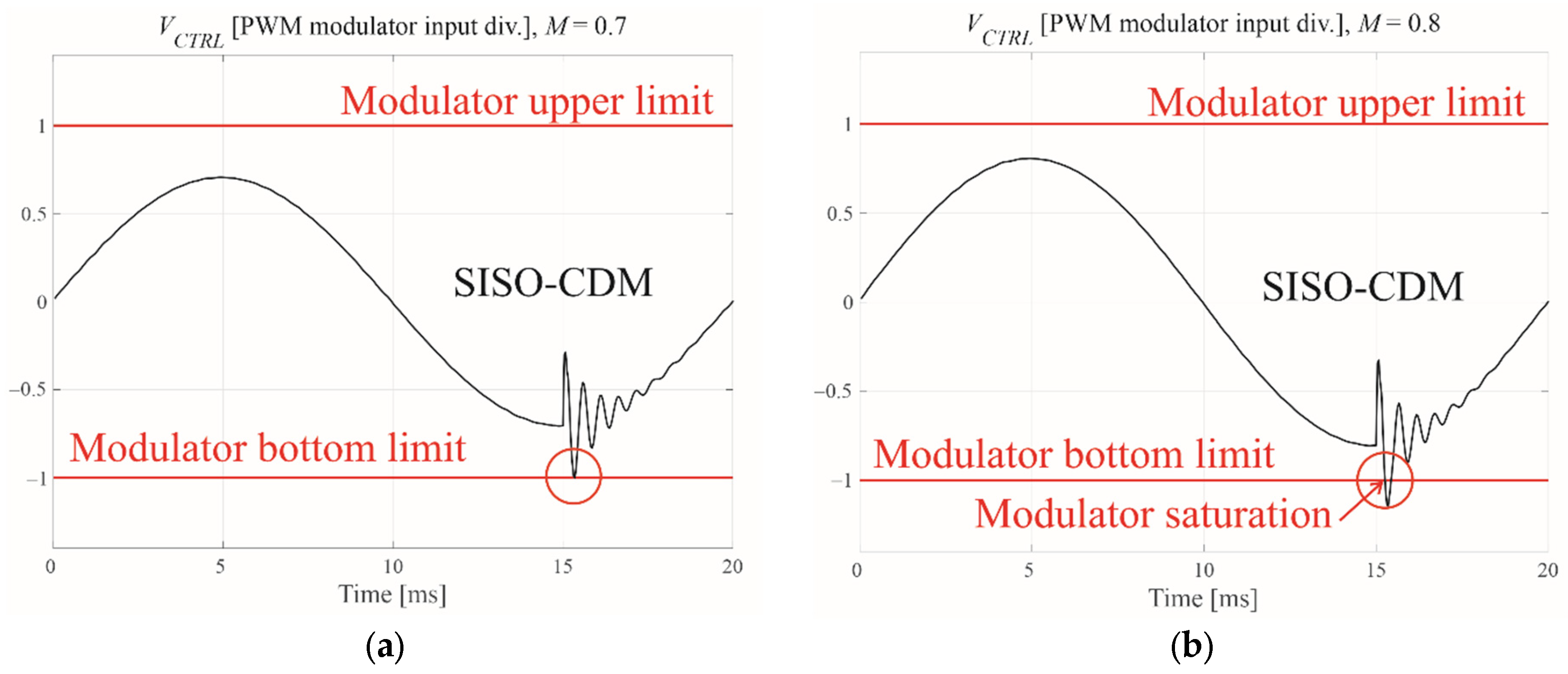
The diagram of the SISO control is presented in Figure 4. The voltage conditioning scales the output voltage amplitude value to the scale of the amplitude of the reference voltage. It sets the output voltage amplitude for the modulation index M = 1 of the reference voltage VREF. In the simulations with the VDC voltage of the VSI, the voltage conditioning coefficient was VREFamp/VDC. However, the modulation index M should be set below unity because it would cause the saturation of the PWM modulator. In our further simulations, when the amplitude VREFamp is equal to unity, we set M = 0.7 and check if the control signal in the PWM modulator input is inside ±1 range, and there is no modulator saturation. M = 0.7 was the highest possible modulation index without saturation in our simulation (it will be shown further).
The inverter output voltage is (31). N and D are from (29) and (30).
v O U T ( z 1 ) = T N R D + S N v R E F ( z 1 ) Z O U T R D R D + S N I O U T ( z 1 )
The characteristic equation of a closed-loop system is Equation (32).
P ( z 1 ) = R ( z 1 ) D ( z 1 ) + S ( z 1 ) N ( z 1 ) = i = 0 n p z i z i
For CDM [8,9,10], a system with a disturbance (Figure 4: IOUT), the degrees of R and S should be equal to or higher than n − 1, where n is the degree of D. For VSI with a plant described by (28), the second order of R and S was assumed (33):
S ( z 1 ) = i = 0 2 s i z i   ,   R ( z 1 ) = i = 0 2 r i z i ,   r 0 = 1
We should solve the Diophantine Equation (34) for r0 = p0 = 1. To find the ri and si coefficients, a matrix Equation (35) should be solved, where pzi are coefficients of the Standard Manabe Form [8,9] in the discrete version. The fifth degree of the Manabe Standard Form is suitable for calculating the coefficients of second-order CDM control for the VSI (35).
( 1 + r 1 z 1 + r 2 z 2 ) ( 1 + b 1 z 1 + b 2 z 2 ) + ( s 0 + s 1 z 1 + s 2 z 2 ) ( a 2 z 2 + a 3 z 3 ) = i = 0 5 p z i z 1
1 0 0 0 0 b 1 1 a 2 0 0 b 2 b 1 a 3 a 2 0 0 b 2 0 a 3 a 2 0 0 0 0 a 3 r 1 r 2 s 0 s 1 s 2 = p z 1 b 1 p z 2 b 2 p z 3 p z 4 p z 5
The coefficients pi of the Standard Manabe Form in a continuous system for the fifth degree of P(s) are the following:
p0(s0) = 1, p1(s1) = p0τ, p2(s2) = 0.4p0τ2, p3(s3) = 0.08p0τ3, p4(s4) = 0.008p0τ4, p5(s5) = 0.0004p0τ5
The time constant of a closed-loop system is τ. The experimentally satisfactory results of the CDM control were achieved for τ = 4Ts or τ = 5Ts (5Ts in simulations, 4Ts in the experimental model). Shorter or longer time constants caused some oscillations for the standard loads.
To find the coefficients of the Standard Manabe Form in the discrete version, the transfer function was discretized using the c2d MATLAB R2021b function with the discretization cycle Ts equal to the switching period (36).
K ( z ) = c 2 d ( 1 i = 0 5 p i ( s ) s i , T s ) = i = 0 5 w i ( z ) z i i = 0 5 p z i ( z 1 ) z i
The result of the discretization is in Table 1.
To keep vOUT = vREF in the steady state, the requirement (37) should be fulfilled. However, in the real VSI, the value of t0 can require some corrections.
t 0 = P ( z = 1 ) N ( z = 1 ) = V D C T s 1 + p z 1 + p z 2 + p z 3 + p z 4 + p z 5 φ 12 g 21 + ( 1 φ 22 ) g 11
The results of solutions (35) and (37) are in Table 2.
The difference control law of the CDM control for the second order of controller nominator and denominator is presented in Equation (38).
v C T R L ( k ) = r 1 v C T R L ( k 1 ) r 2 v C T R L ( k 2 ) + t 0 v R E F s 0 v O U T ( k ) s 1 v O U T ( k 1 ) s 2 v O U T ( k 2 )
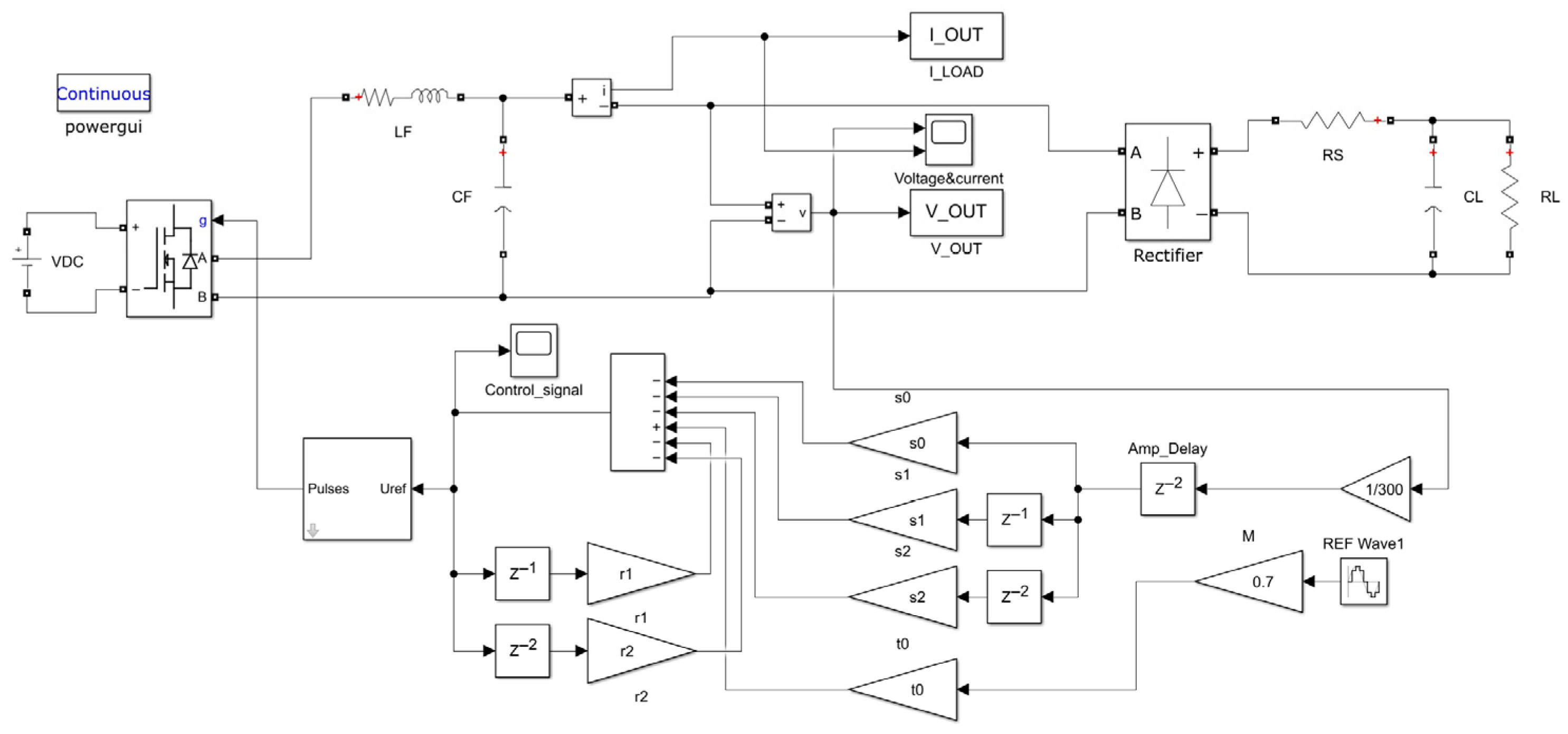
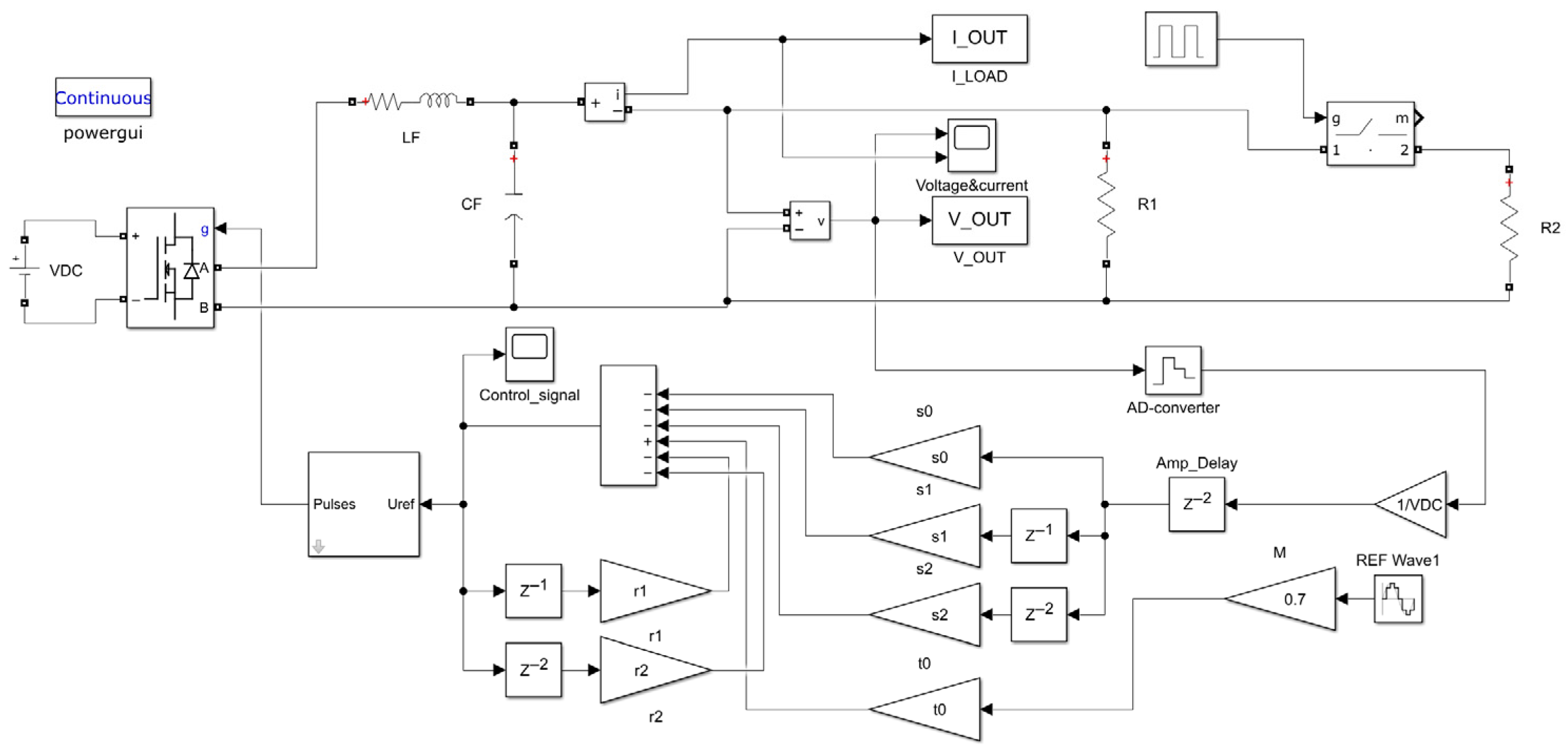
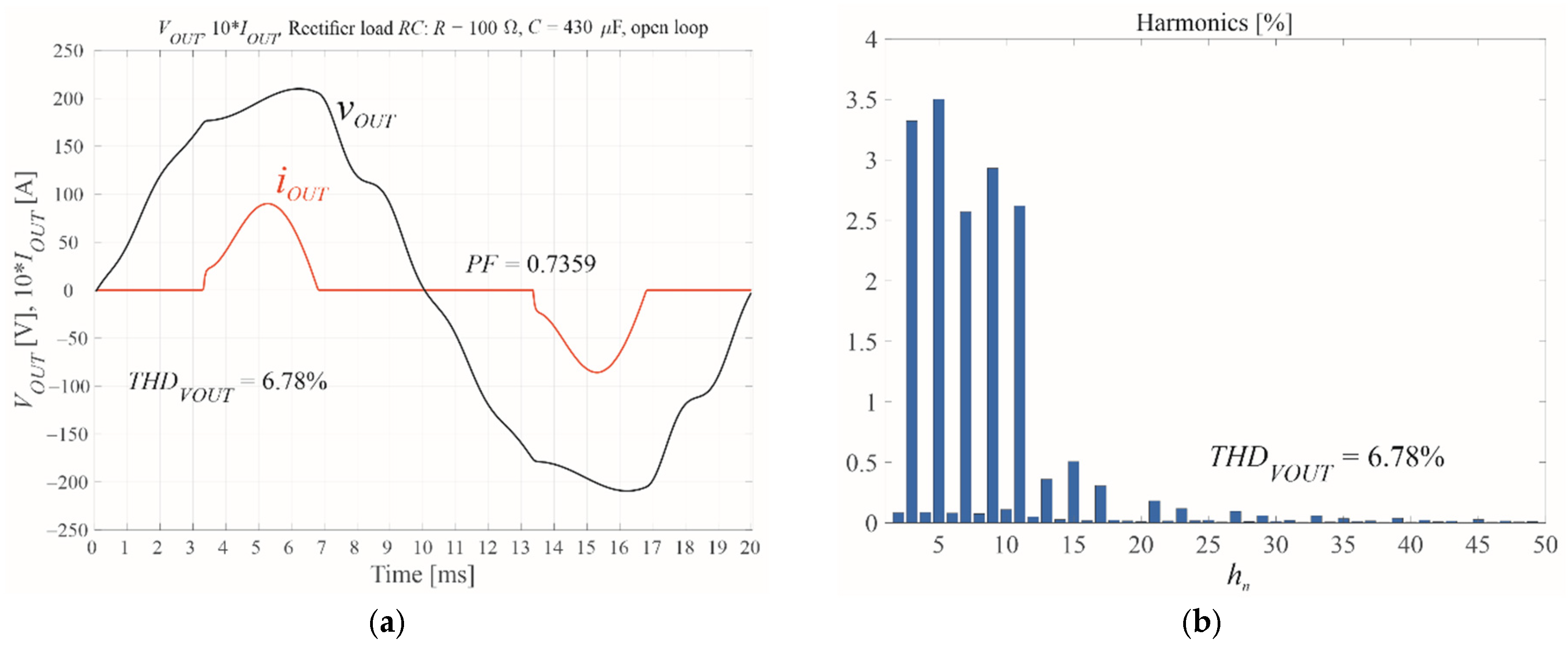
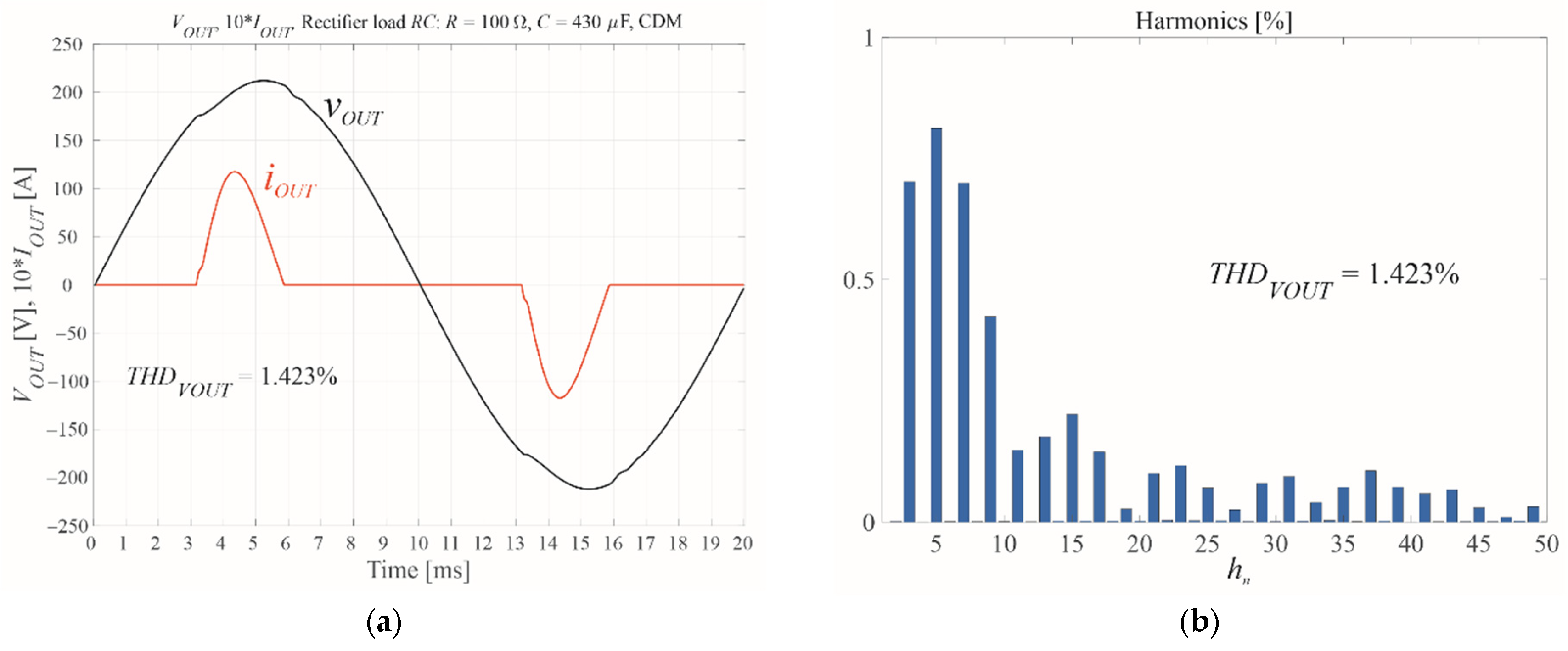
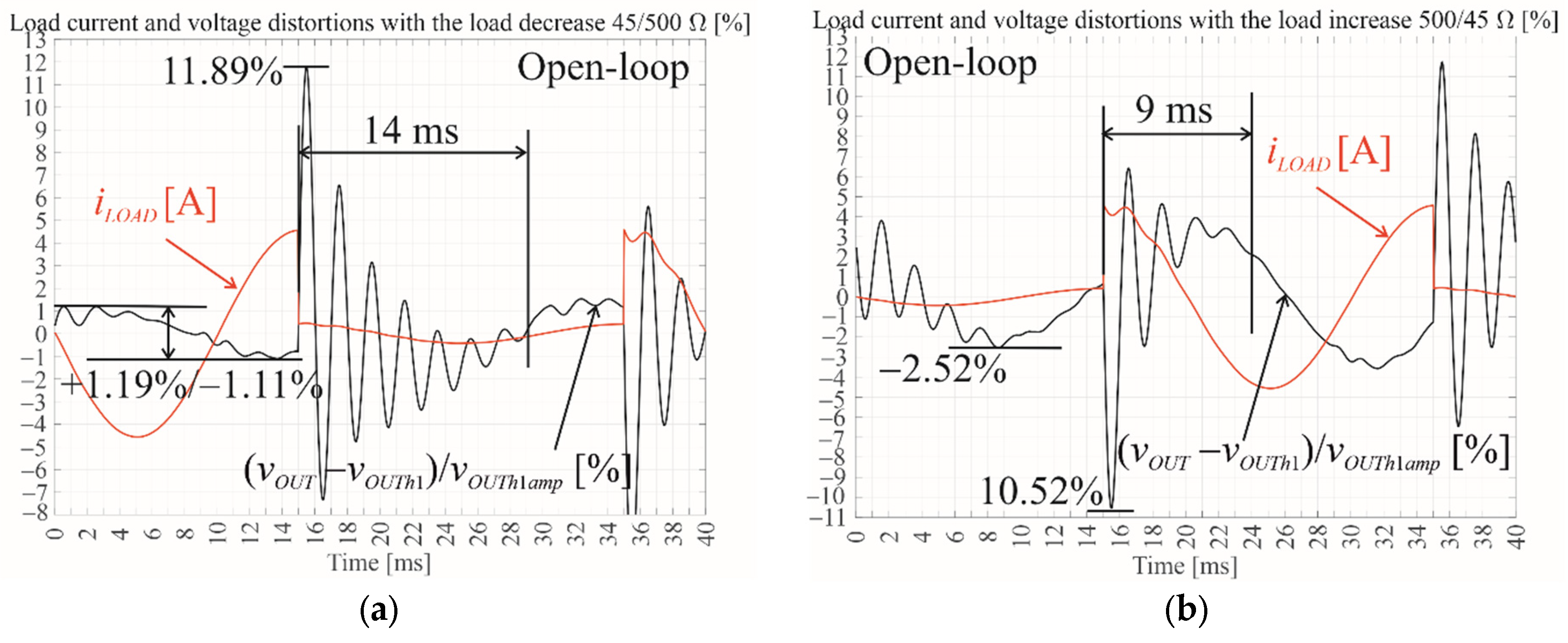
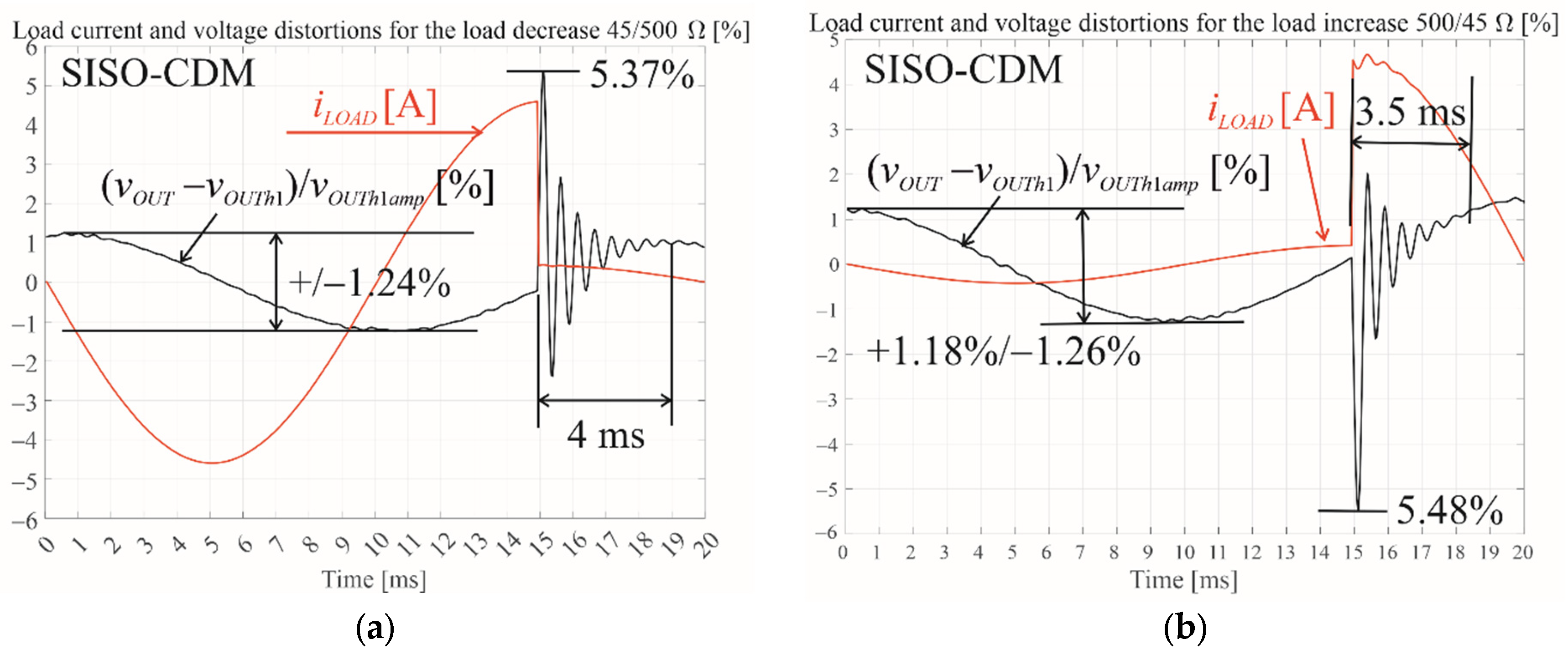
Figure 5 presents a simulation model diagram (MATLAB 2021b) for the CDM control for the rectifier RC load (100 Ω || 430 µF, Rs = 1 Ω, VREFamp = 1, M = 0.7), and Figure 6 presents the dynamic step load 45/500 Ω and 500/45 Ω. Figure 7 presents the distortions of the output voltage for the open loop for (a) the rectifier RC load (100 Ω || 430 µF) and (b) the output voltage harmonics’ spectrum. Figure 8 presents the same dependences as Figure 7, but for CDM control. Figure 9 presents the distortions for the open loop for (a) the step load decrease of 45/500 Ω, and (b) for the step load increase of 500/45 Ω. Figure 10 presents the same dependences as Figure 9, but for CDM control.
The discussion of the simulation results for CDM control for the standard loads shows that for the rectifier RC load (PF ≈ 0.7), the output voltage THD is reduced from 6.78% to 1.42%. The overshoot for the step load decrease 45/500 Ω is reduced from 11.89% to 5.37%, and the settling time is reduced from 14 ms to 4 ms. The undershoot shoot for the step load increase 500/45 Ω is reduced from 10.52% to 5.48%, and the settling time is reduced from 10 ms to 3.5 ms. The output voltage follows its first harmonic in the steady state in a similar way (up to ±1.25% of error). It should be noted that the load current is forced by CDM to change its shape, thereby reducing the output voltage drop when the rectifier begins conducting. For the MISO control, the shape of the current will be more complex. The highest modulation index for which there is no modulator saturation is M = 0.7 (Figure 11). A lower modulation index than 0.7 would be advantageous in control, but unreal.

4. MISO Passivity-Based Control

The energy in the inverter system is stored in the filter inductor and capacitor. The Hamiltonian function (39) describes this energy stored in the system. The idea of the Passivity Based Control (PBC) [3,7,12,13,14,15,16,17,18] is based on the fact that the energy stored in the VSI system should be lower than the energy delivered to the inverter system. The idea of PBC is similar to the Lyapunov approach [12]. The control is realized by “injecting” virtual resistance Ri, which is a substitute for the current gain. In [3,12], the additional gain Kv for the output-voltage error was used in the control law of the improved PBC [7]. Output current is treated as the independent variable.
x = [ v O U T C F   i L F L F ] ,   H ( x ) = 1 2 ( L F i L F 2 + C F v O U T 2 )
The equilibrium of a closed-loop system is asymptotically stable [22] if the Hamiltonian function H(e) has a minimum in x = xref (40).
e = x x r e f ,   H ( e ) x x = x r e f = 0 ,   2 H ( e ) x 2 x = x r e f > 0
A negative value of the time derivative H(e) is a requirement of the system passivity (41).
d H ( e ) d t < 0
The PBC law is created from Equation (42) [3] for a closed-loop system and Equation (43) for an open-loop system.
e ˙ = [ 0 1 1 0 ( R L 0 0 0 + R i 0 0 K v ) ] 1 L F 0 0 1 C F e
x ˙ = [ 0 1 1 0 R L 0 0 0 ] 1 L F 0 0 1 C F x + V D C 0 m + 0 1 i O U T
The discretized PBC law [7,31] is (44) and (45).
v C T R L ( k ) = R i i L F ( k ) + ( R i + R L ) i L F r e f ( k ) + L F i L F r e f ( k ) i L F r e f ( k 1 ) T s + v R E F ( k )
i L F r e f ( k ) = K v [ v R E F ( k ) v O U T ( k ) ] + C F v R E F ( k ) v R E F ( k 1 ) T s + i O U T ( k )
The system with PBC is stable for RL + Ri > 0 (RL is always >0, and we assign that Ri > 0) and Kv > 0. In this case, the roots of the continuous characteristic equation of the closed-loop PBC system are in the left half s-plane [7]. The upper limit of the PBC gains is a result of the restriction of the output voltage control change speed. For the three-level PWM modulation used, it is VDC/Ts (in one switching period, the output voltage cannot increase more than VDC). This restriction follows (46) [22].
d v C T R L ( k T s ) d t V D C T s
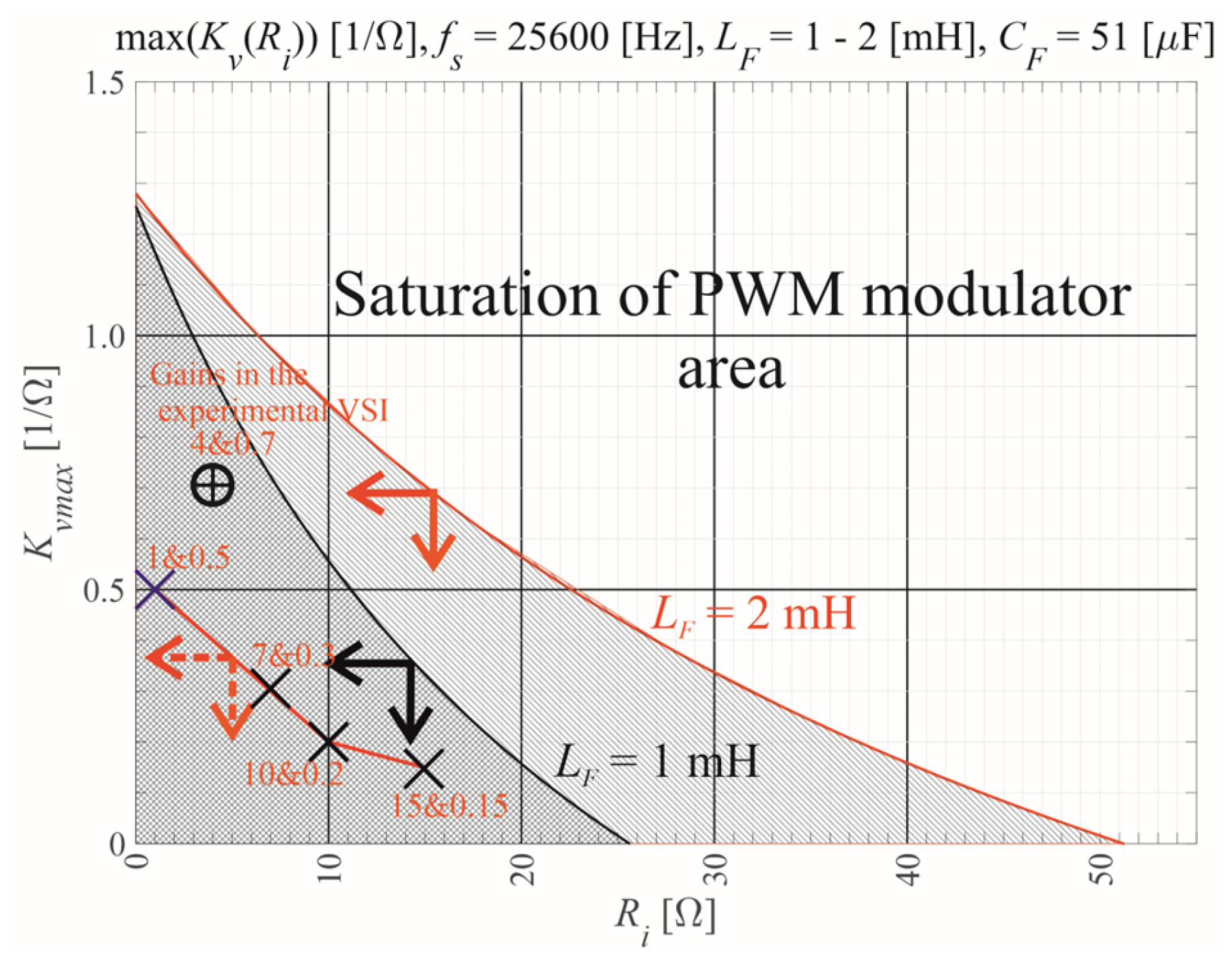
From (44)–(46), for the worst case of control, the inverter load RLOAD = ∞, for the system where we can neglect existing delays, the approximated restriction is (47), and the allowable areas of gains are presented in Figure 12.
K v [ L F + ( R i + R L ) T s ] 1 L F C F + R i L F < f s
The allowable areas of gains from (47) are below the red curve for LF = 2 mH or below the black curve for LF = 1 mH. The higher gains result in the lower output voltage error and faster convergence. The presented restriction (47) gives approximate results useful for initially setting up the PBC controller. RL = 1 Ω has no serious influence on the allowable area because we set much higher Ri. The crosses in Figure 12 point to the values of Ri and Kv: one and 0.5, seven and 0.3, 15 and 0.15, and present the real borderline of the maximum gains for LF = 2 mH in simulations. Above this line, the oscillations in the control system begin. The values of the gains tested in the experimental VSI are in the circle. They are also in the allowable area.
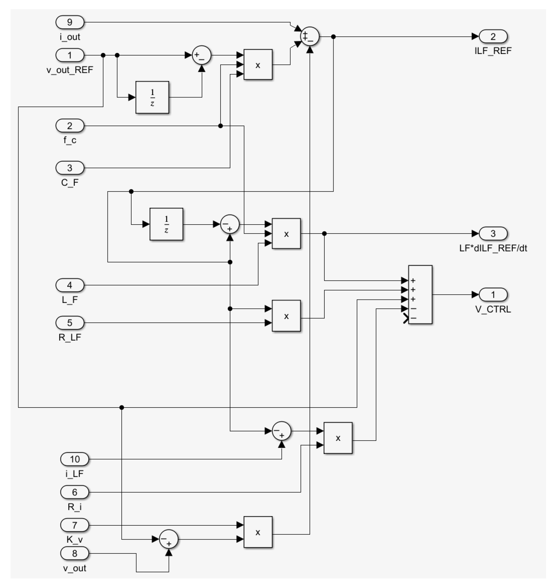
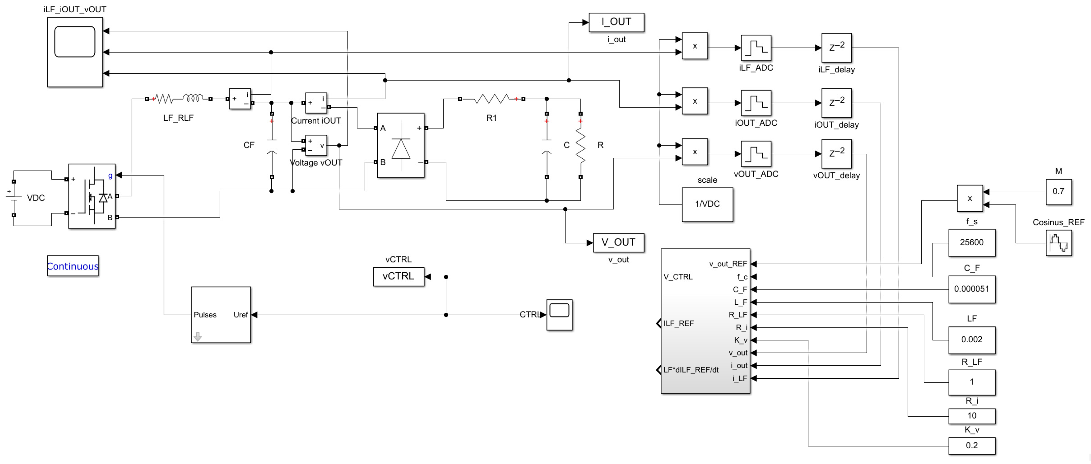
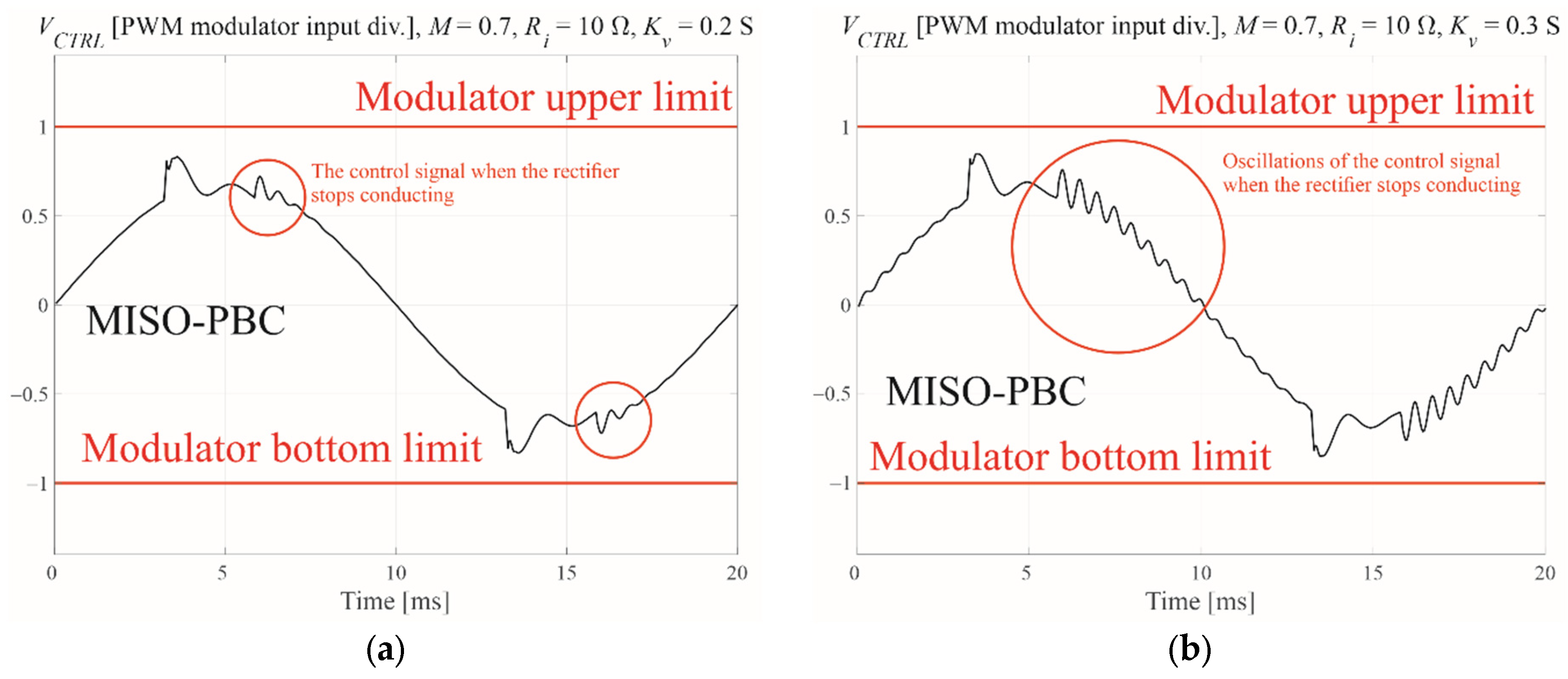
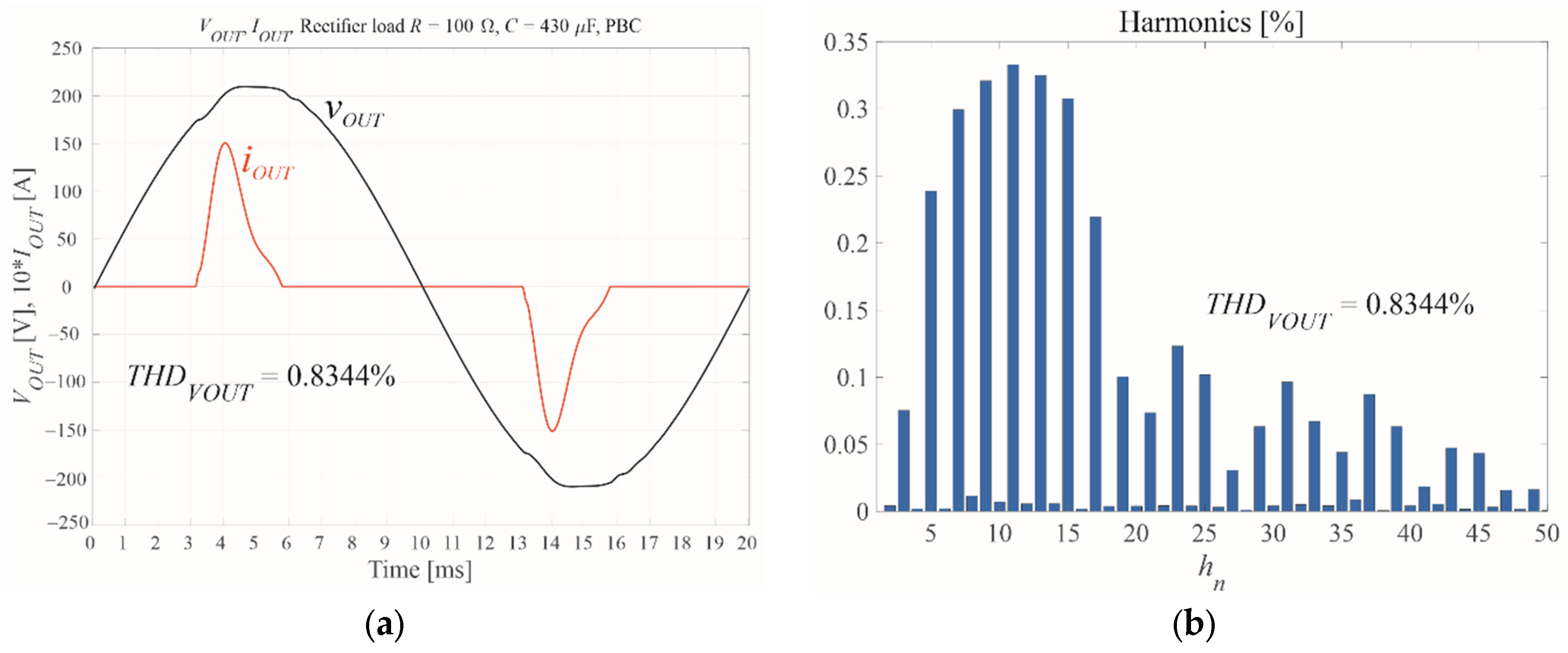
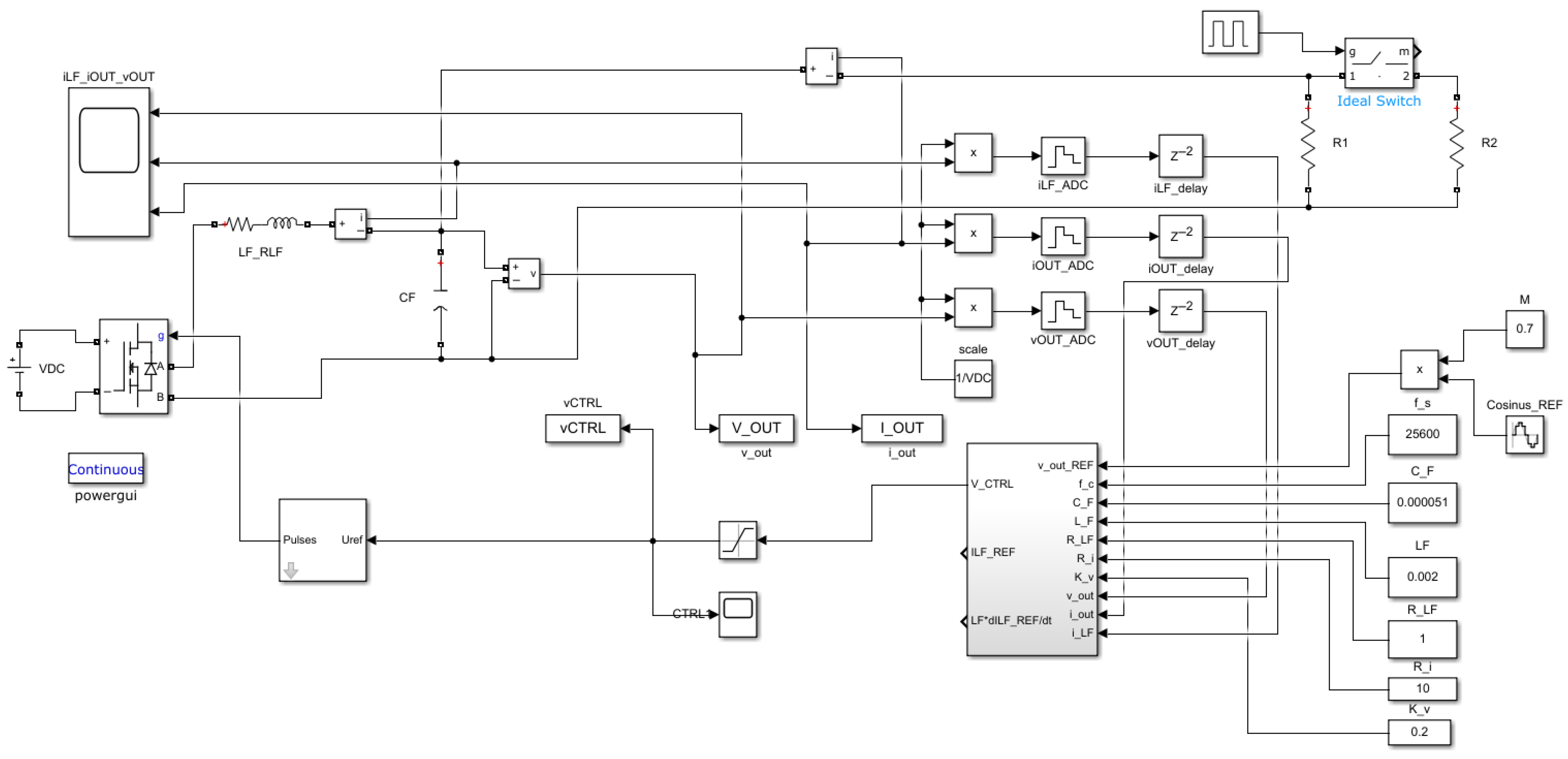
Figure 13 presents the PBC controller module that realizes the control law Equations (40) and (41). Figure 14 presents the simulation module diagram of VSI with the PBC controller from Figure 13 and the rectifier RC load (430 µF || 100 Ω). The gains were set Ri = 10 Ω and Kv = 0.2 S. The other set of allowable gains Ri and Kv are one and 0.5, seven and 0.3, 15 and 0.15. They are from the allowable region of gains from the diagram in Figure 12, when the PBC is slower than the PBC modulator speed. They mark the line above which oscillations occur for LF = 2 mH. The simulated restrictions are harder than calculated from (43). Figure 15 presents the control voltage for the different sets of gains (oscillations begin for the higher gains). Figure 16 shows the distortions of the output voltage for the PBC (Ri = 10 Ω and Kv = 0.2 S) for the rectifier RC (100 Ω|| 430 µF) load and the output voltage harmonics spectrum. The values further adjusted in the experimental VSI (Ri = 4 Ω and Kv = 0.7 S) differ from those in simulations, but they are from the same allowable area. The distortions of the output voltage are lower (THDVOUT = 0.83%) than in the case of SISO-CDM control (1.42%) for the same nonlinear load.
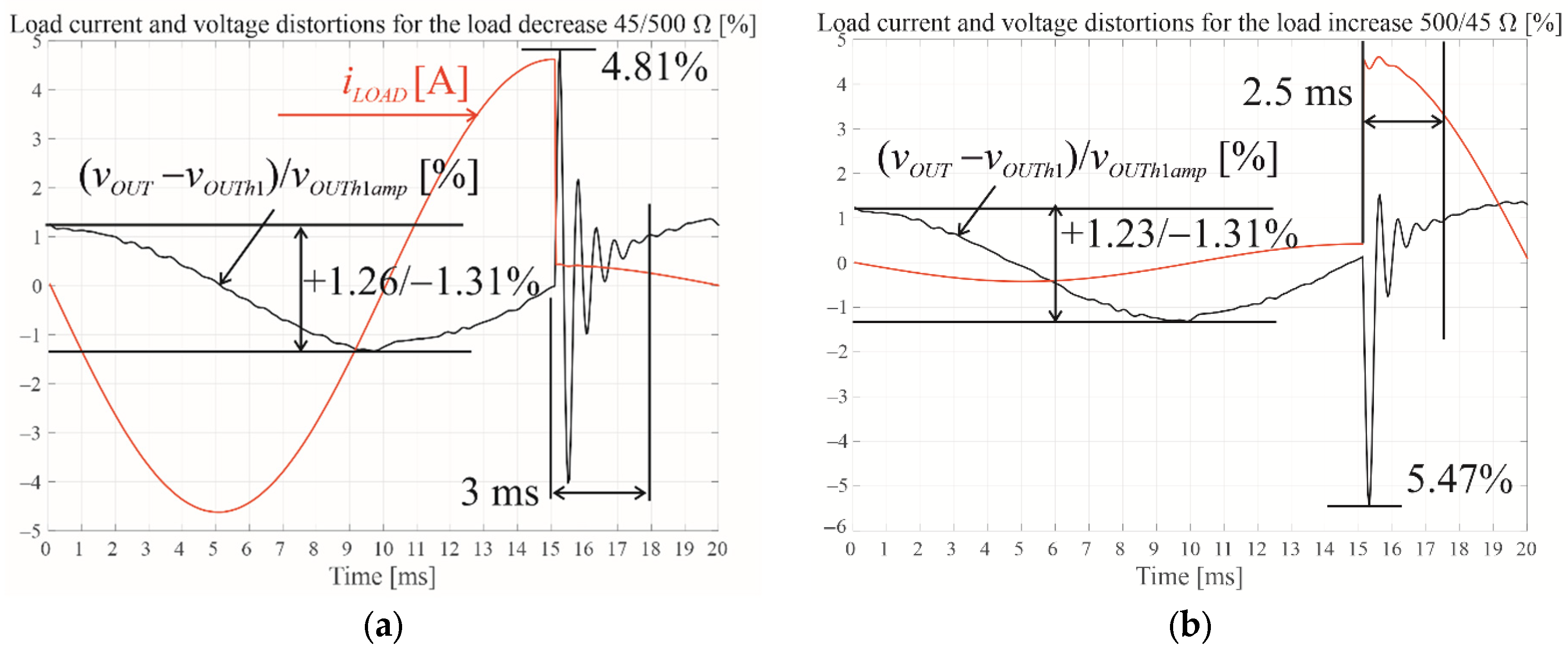
The discussion of the simulation results for PBC for the standard loads shows that for the rectifier RC load (PF ≈ 0.7), the output voltage THD is reduced from 6.78% to 0.83%—better than in the case of SISO-CDM (1.42%). Figure 17 presents the simulation module diagram of VSI with the PBC controller from Figure 13 for the step load. The overshoot for the step load decrease 45/500 Ω is reduced from 11.89% to 4.81%, and the settling time is reduced from 14 ms to 3 ms (Figure 18a). The undershoot shoot for the step load increase 500/45 Ω is reduced from 10.52% to 5.47%, and the settling time is reduced from 10 ms to 2.5 ms (Figure 18b). The overshoot and undershoot of the output voltage are similar to the results of CDM control (Figure 10a,b). The settling time is a bit shorter. The output voltage follows its first harmonic in the steady state (up to ±1.3% of error), in a similar way to CDM control. It should be noted that the load current is forced by MISO-PBC to change its shape more than in the case of MISO-CDM control. The highest modulation index for which there is no modulator saturation is M = 0.7, as in the case of CDM.

5. MISO Deadbeat Control

The deadbeat control [19,20,21] places all poles of the closed-loop transfer function at the origin of the z-plane. The deadbeat control is useful in linear systems. One of the advantages of the deadbeat control is reaching the steady state of the output in a countable number of time periods equal to the order of the system. A. Kawamura [19] described that for the second-order model of the inverter system, when the output voltage value can be equal to the reference value in the next k + 1 switching period. This statement is used in One-Sample-Ahead Preview Control (OSAP), also presented in the newer papers [20,21].
The deadbeat OSAP law of the inverter is based on the assumption vOUT(k + 1) = vref(k + 1). Deadbeat control law has no assigned gains for the voltage or current. Its operation depends on the parameters of the control system and the switching period. Deadbeat control is very sensitive to the values of parameters and to delays in the plant’s open-loop transfer function. Version SISO of the deadbeat control is practically useless for VSI control. Only using all the state variables (output voltage, inductor current, and output current that are dependent on the parameters of the inverter) as inputs of the MISO-OSAP deadbeat control (Figure 19) can lead to acceptable control results for the standard loads in the system without noticeable delays.
If reasonable delays exist, the state variables should be predicted. The first equation of (13) is (48).
v O U T k + 1 = φ 11 v O U T k + φ 12 i L F k + φ 13 i O U T k + g 11 T s V D C v C T R L ( k )
If we assume v O U T k + 1 = v r e f k + 1 , we receive MISO-OSAP law (49).
v C T R L k = 1 g 11 V D C T s [ v r e f k + 1 φ 11 v O U T k φ 12 i L F k φ 13 i O U T k ]
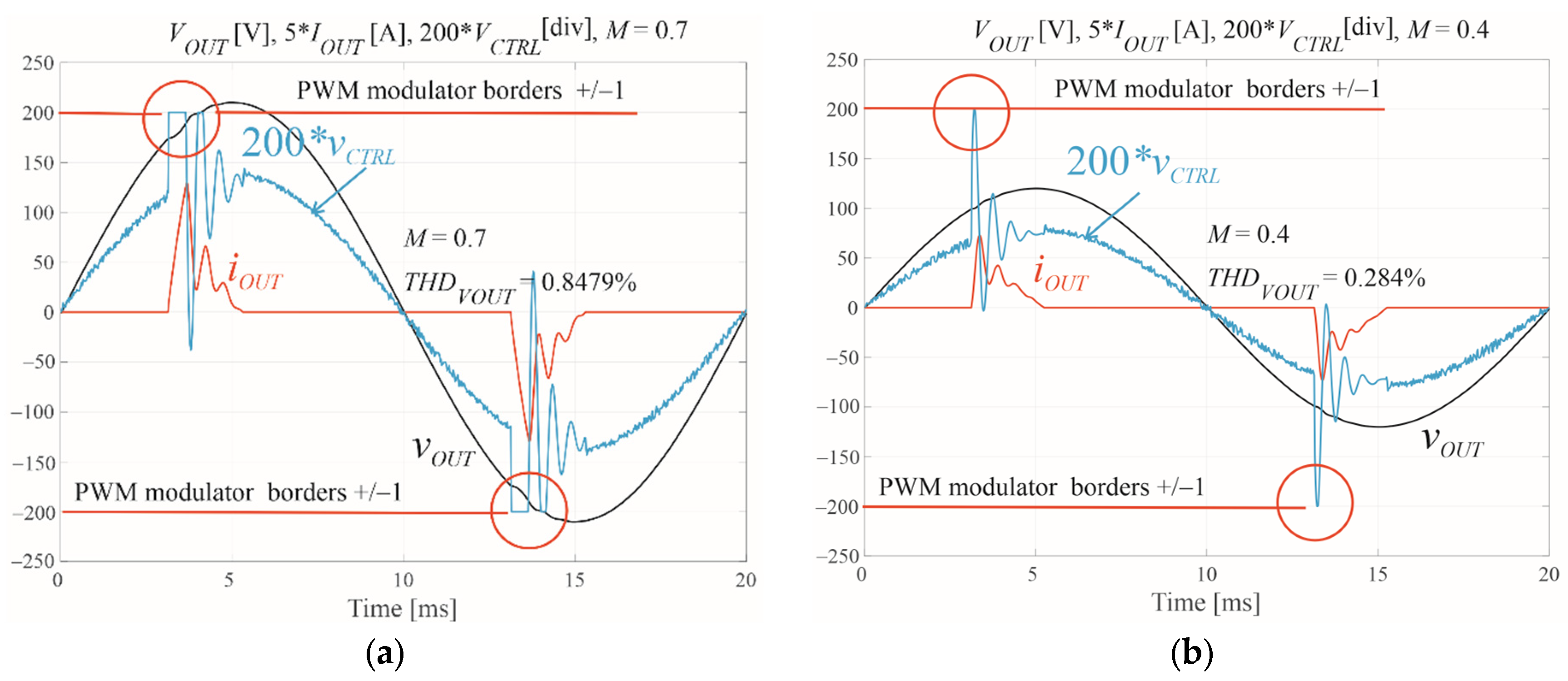
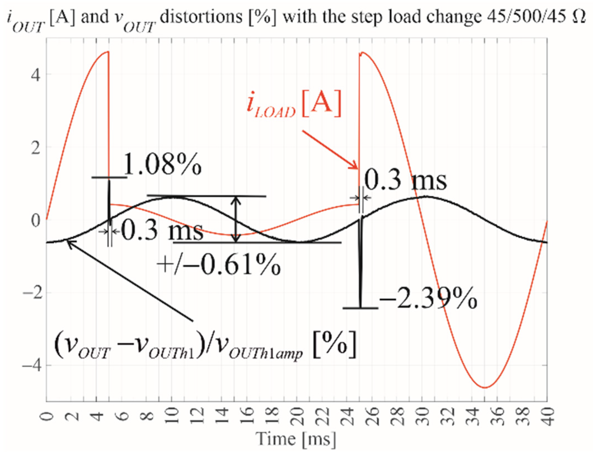
We should note that (49) does not depend on VDC because its value simplifies to the same value as VDC in Equation (24) of g11. There are two problems with MISO-OSAP. The first is a very high amplification of the output voltage error. The result is the required reduction in the modulation index M. As shown in Figure 20, the value M = 0.7, previously used for PBC, leads to the saturation of the PWM modulator, which slightly increases the output voltage distortions (THDVOUT = 0.85%) for the nonlinear rectifier RC load. The highest value of the modulation index for which there is no saturation of the modulator in the case of the nonlinear load is M = 0.4 (Figure 20). Such a low value of the modulation index is unacceptable in the real world; however, the output voltage distortions are very low for M = 0.4 (THDVOUT = 0.284%). M = 0.7 will be further used in simulations. The second problem is the high sensitivity of MISO-OSAP to delays. The output overshoots (1.08%), undershoots (2.39%), and settling time (equal to 0.3 ms) are really very low because the MISO-OSAP is the fastest (Figure 21).
The system MISO-OSAP, with results of control in Figure 20 and Figure 21, has only modeled an analog-to-digital converter (ZOH) and a modulator with structural delay. It can be seen that MISO-OSAP “carves” the waveform of current for the rectifier RC load more than any other MISO control. Any additional delay in the measurement channels (it was 2Ts in previous examples of SISO-CDM and MISO-PBC) causes oscillations of the output voltage. The solution is to use the Luenberger Observer to predict state variables.
The full-order state Luenberger Observer [31,32,33] is a linear solution (e.g., a Kalman filter requires much more calculations) for the three input state variables prediction in the system with delays with MISO-OSAP deadbeat controller that is unstable even for an additional delay equal to the single switching period Ts, for the standard nonlinear load. The Luenberger Observer and other similar linear observers are frequently used in inverters’ control systems [34,35,36,37]. In the full-order state Luenberger Observer (46), all the state variables are measured to predict them in the next switching periods. Comparing the state Equations (13)–(15) with equations of the predicted state variables [ v ^ O U T , i ^ L F , i ^ O U T ]T (50) and (51), the output matrix CL (51) is different from the CD (15) because now all the state variables are in the outputs of the Luenberger Observer (not only the output voltage).
x ^ ( k + 1 ) = A D x ^ ( k ) + G D T O N ( k ) + L [ y ( k ) C L x ^ ( k ) ]
y = x ,   C L = 1 0 0 0 1 0 0 0 1
The matrix of Luenberger Observer gains for three state variables [vOUT, iLF, iOUT]T is (52).
L = l v O U T 0 0 0 l i L F 0 0 0 l i O U T
We can estimate the values of the components of the matrix of the Luenberger Observer gains by analyzing the equation of the system error (53).
e k + 1 = x k + 1 x ^ k + 1 = ( A D L C L ) e ( k )
The characteristic equation of the full-state Luenberger Observer is (56) derived from (54) and (55).
det ( I z A D + L C L ) = 0
det z φ 11 + l v O U T φ 12 φ 13 φ 21 z φ 22 + l i L F φ 23 0 0 z 1 + l i O U T = 0
z 1 + l i O U T z φ 11 + l v O U T z φ 22 + l i L F φ 12 φ 21 = 0
The “separation theorem” [38] states that setting the three roots z1, z2, and z3 of the characteristic equation of the Luenberger Observer (56) is independent of the closed-loop feedback control. The observer should provide a faster convergence to zero of the observation error than the transient process in a closed-loop system. For the discrete system, the roots of the Luenberger characteristic Equations (55) and (56) should be closer to zero on the z-plane than the roots of the characteristic equation of the closed feedback-loop system. This requirement cannot be met for the deadbeat control that has the poles of the closed-loop system equal to zero, and there is no simple algorithm for setting the Luenberger gains. Different algorithms for calculating the values of the linear observer characteristic equation roots compared to the closed-loop system characteristic equation roots were presented in [38,39,40]. In [38], the design of the Luenberger Observer ensured that its dynamics would be three times faster than the fastest pole of the plant. It is possible to use the poles placement acker() MATLAB function to get the pole position of the state observer [39] and further to obtain its gain matrix. Always, the eigenvalues of the continuous Luenberger Observer characteristic equation [40] should have real negative parts. In our case of deadbeat control, we can solve Equation (56) by setting the Luenberger gains such that the absolute value of the three roots z1, z2, and z3 is lower than unity (the roots are inside the unit circle in the z-plane). The observer gains are initially assigned as positive values. The absolute value of the first root z1 (57) is below unity if, according to (58), liOUT < 2.
z 1 = 1 l i O U T
1 l i O U T < 1
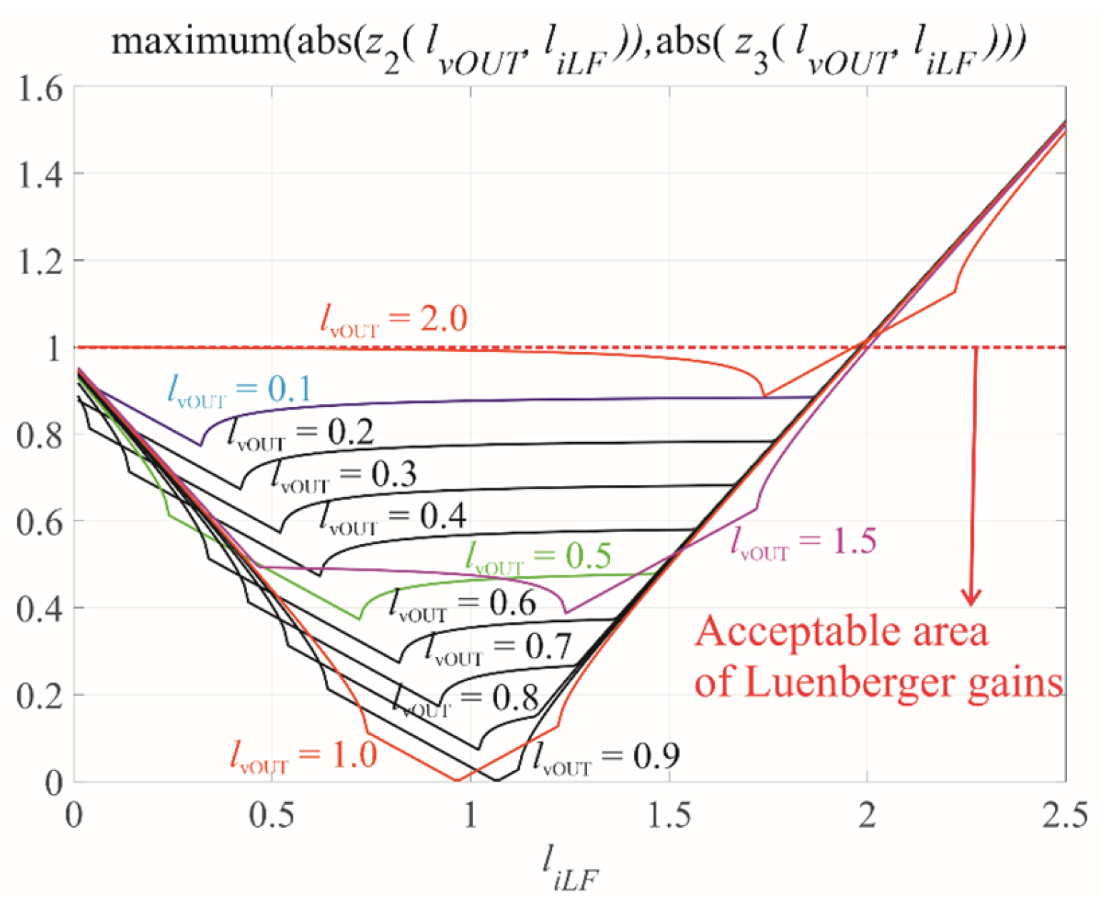
The solution of Equation (56), finding z2 and z3, is graphically presented in Figure 22, where lvOUT and liLF are parameters of the solution. The final approximated restriction for lvOUT, liLF, liOUT > 0 is lvOUT < 2, liLF < 2, liOUT < 2. However, the lowest values of |z1|, |z2|, and |z3| (the fastest Luenberger Observer) are for lvOUT ≈ 1, liLF ≈ 1, liOUT ≈ 1. Finally, the gains lvOUT, liLF, liOUT of the Luenberger Observer (LO) should be adjusted starting from the unity value in the allowable area (Figure 22) by the trial method for the particular design case of the MISO-OSAP-LO.
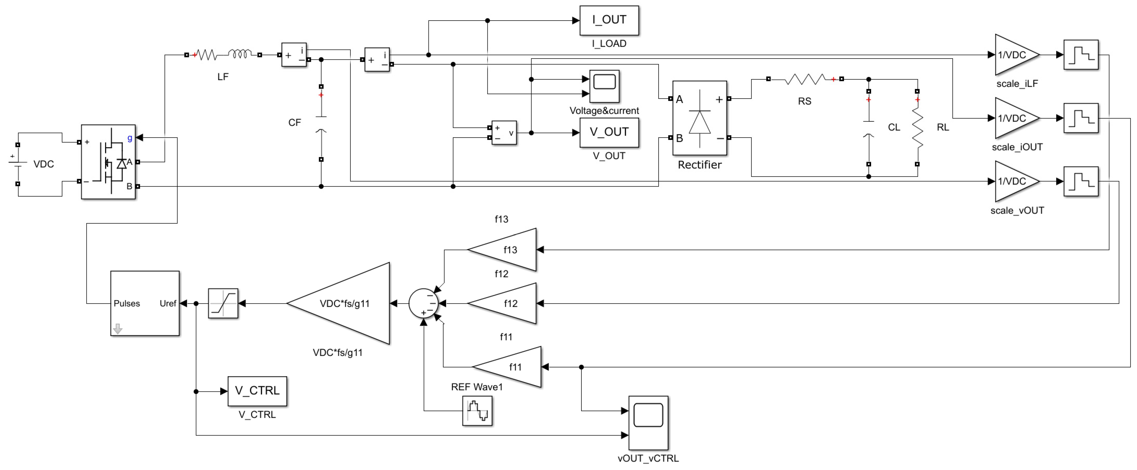
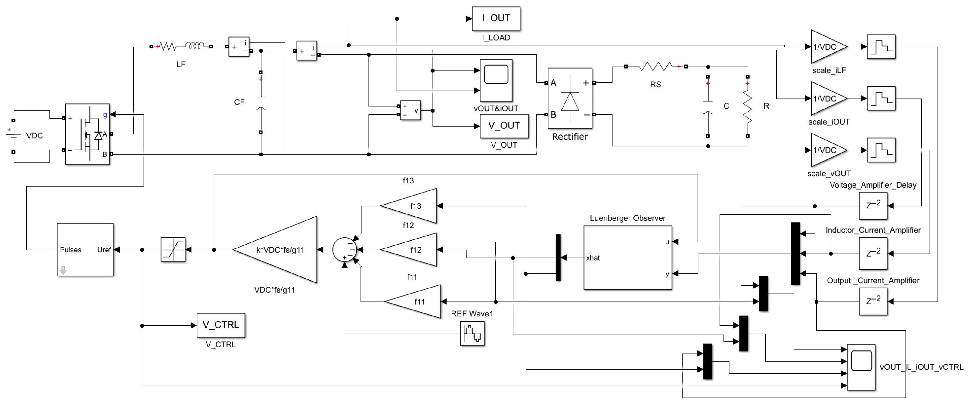
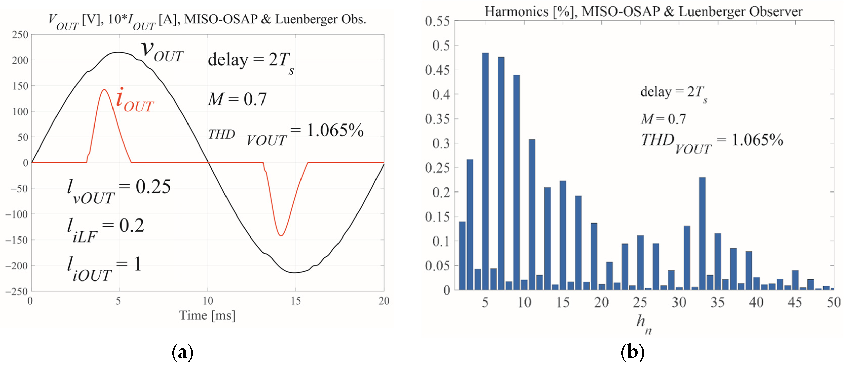
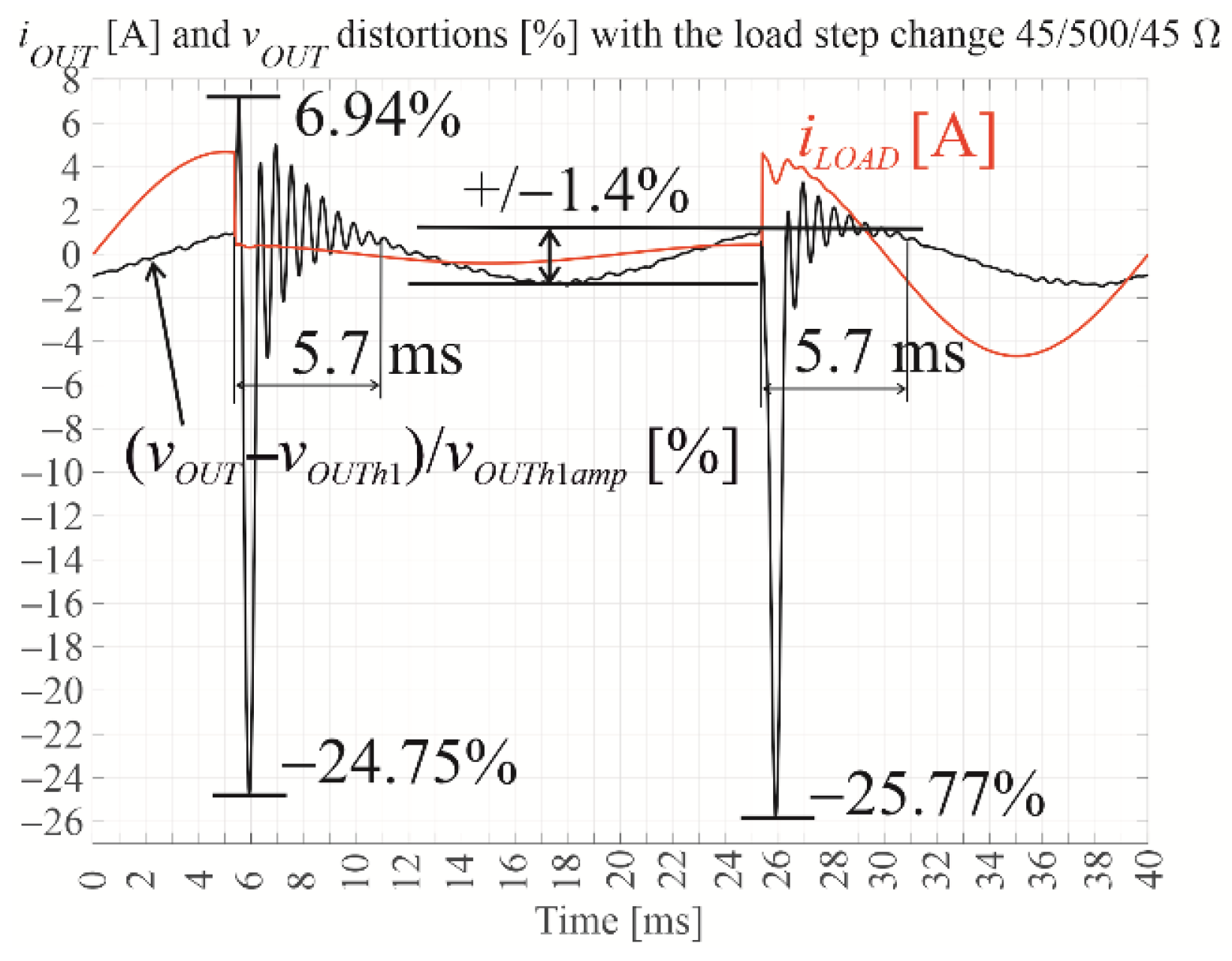
Figure 23 shows a simulation module schema of VSI with the MISO-OSAP-LO controller and the rectifier RC load (430 µF || 100 Ω) with additional delays 2Ts in the measurement channels. Figure 24 presents the distortions of the output voltage for the MISO-OSAP-LO control for the rectifier RC (100 Ω || 430 µF). The THDVOUT of the output voltage for the rectifier RC load is similar to the result for MISO-PBC, but the voltage overshoots and undershoots are unacceptably high. The settling time is slightly longer than for MISO-PBC. It can be seen that using the Luenberger Observer allows the system to operate with measurement channel delays but significantly degrades the closed-loop dynamic properties (Figure 25).

6. The Discussion of the Properties of Simulated Control Systems

The simulations were performed for fs = 25,600 Hz, for the additional delays in the measurement channels equal to 2Ts for the rectifier RC load (430 µF || 100 Ω) and step load change 45/500/45 Ω, for modulation index M = 0.7 (even though it could, in some cases, lead to the saturation of the modulator e.g., Figure 20).
The best results are for the fastest MISO-OSAP (it is 10 times faster than MISO-PBC) but it can properly work only in the system without additional delays of the measurement channels (only the structural delay of the PWM modulator and analog-to-digital conversion delay exist in the simulation model, totaling one Ts delay; in the same switching period we measure variables and store them in modulator register). Modification of MISO-OSAP with the prediction of the state variables by means of the Luenberger Observer worsens the dynamic parameters of the MISO-OSAP-LO controller. So, both MISO-OSAP and MISO-OSAP-LO controllers can be useless in real applications. MISO-PBC has slightly better parameters of control than SISO-CDM, but it is more expensive. It requires three measurement channels (the output voltage, the inductor, and the output currents). Additionally, the adjustment of PBC requires careful adjustment of two gains, while the adjustment of CDM requires adjustment only of the time constant. So, it should be discussed if, in the particular case, using MISO-PBC is cost-effective. There is one more parameter that is not usually discussed—the distance of the output voltage from its first harmonic in the steady state. For the simulation of all the controls, it was not more than ±1.5%. However, the experimental data are a bit different. The further experimental verification concerns SISO-CDM and MISO-PBC controls.
The energy that is delivered to the load in one fundamental period (20 ms) is always the same for the open-loop and all kinds of control systems. The differences are in the shape of the current waveform and, consequently, the distortions of the sinusoidal output voltage waveforms. In the case of the rectifier RC load, the MISO type of control forces a faster increase in the load current when the rectifier begins to conduct. This increase in the inductor current (59) [41] is restricted by the maximum possible increase in the filter inductor current. In case of VDC = 85 V, M = 0.7, R = 100 Ω, C = 430 µF, LF = 0.002 H, CF = 51 µF, the maximum possible inductor current increase when the rectifier begins to conduct is about 17,300 A/s, neglecting the serial resistances.
I L t V D C 1 M 1 1 3 50 R C / L F
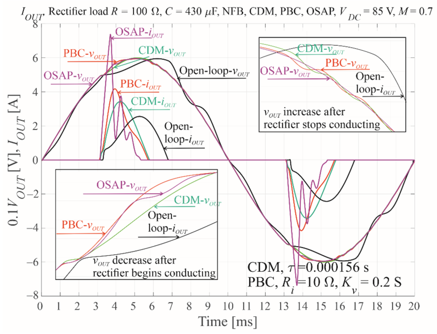
For an open-loop system, the maximum increase (for the almost linear part of the current slope) of output current is 1452 A/s; for SISO-CDM control, the maximum increase in output current is 4218 A/s; for MISO-PBC: 7454 A/s; for MISO-OSAP: 14,296 A/s (MISO-OSAP in the system without additional delays), Figure 26. The fastest increase in the current in the output filter capacitor (CF = 51 µF) is about 300 A/s. So, in the worst case, the increase in the inductor current (it is the sum of the output current and the filter capacitor current) will not reach the border value (59). The presented calculations demonstrate that the MISO control systems lead to a faster increase in the output current, thereby reducing the decrease in output voltage (the decrease under its first harmonic) after the rectifier begins to conduct. What is more, the MISO control systems decrease the output current waveform when the rectifier stops conducting, reducing the output voltage increase (over its first harmonic). At this moment, all the inductor current flows to the filter capacitor (Figure 26).

7. The Experimental Verification

It was presented in [42] that for experimental verification, we can use the Real-Time Interface (e.g., dSpace and MATLAB software with MicroLabBox RTI 1202 hardware) or create a software for the chosen microprocessor—in our case, STM32F407VG (39 Chemin du Champ-des-Filles, 1228 Plan-les-Ouates, Geneva, Switzerland). Using the microprocessor control in the experimental VSI is closer to the final device design, and it requires more sophisticated (as in the real device) scaling of the measured voltage and currents.
It is straightforward to implement the control law equations in the STM32F407VG microprocessor using the two channels, Channel 1 and Channel 2, of its TIMER1. If we have fTIM = 84 MHz at the input of TIMER1, and we assign fs = 25,600 Hz, the approximated maximum peak-to-peak amplitude of the control signal is fTIM/fs = 3281.25. Therefore, the amplitude of the sinusoidal control signal vCTRL (calculated in the control law procedure) can be up to 1640, and the peak-to-peak amplitude can be up to 3280. Channel1Pulse register drives S1, Channel2Pulse register drives S3 from Figure 1.
The input controller signals are measured by the analog-to-digital converter in the range of −4095 to 4095. So, the measured amplitude of the nominal output voltage can be set to 3000 (by means of a potentiometer). The same adjustment should be done in the current measuring channels for the nominal load, Rnom. It should correspond to a value of 1640 in the PWM unit. The scaling factor of the measured output voltage is 1640/3000. The margin for dynamics is obtained by setting M < 1. If the nominal load was 50 Ω, the scaling factor of the output current should be (1640/3000)/Rnom. The scaling factor of the inductor current should take into account the filter capacitor current, and it should be (1640/3000)/(Rnom||1/(2π50CF)). The used parameters are VDC = 85 V, M = 0.7, LF = 0.002 H, CF = 51 µF, R = 100 Ω, C = 100 µF or 430 µF.
MISO-OSAP was very sensitive to the additional delays in the measurement channels. The prediction in MISO-OSAP-LO had advantages for harmonic disturbances but disadvantages for the dynamic load. So, the experimental VSI was tested with SISO-CDM and MISO-PBC controllers.
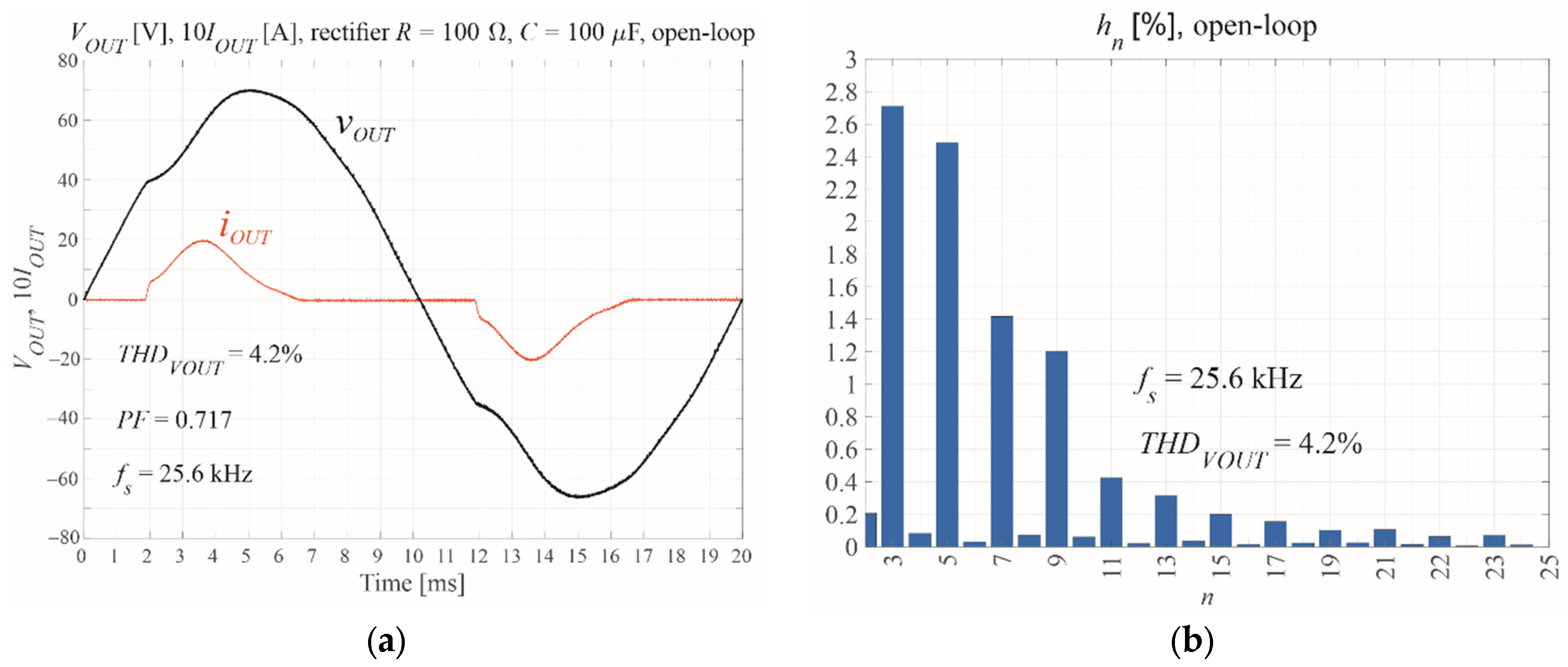
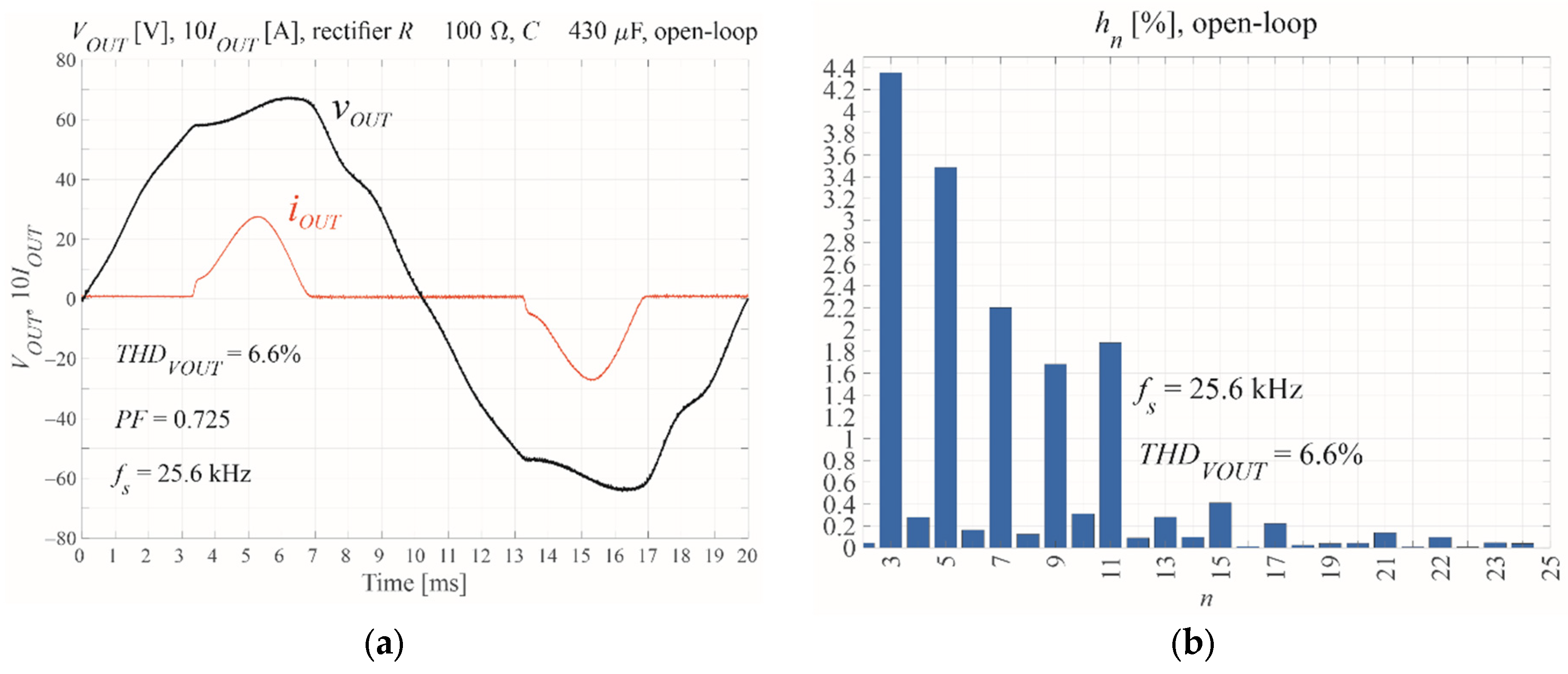
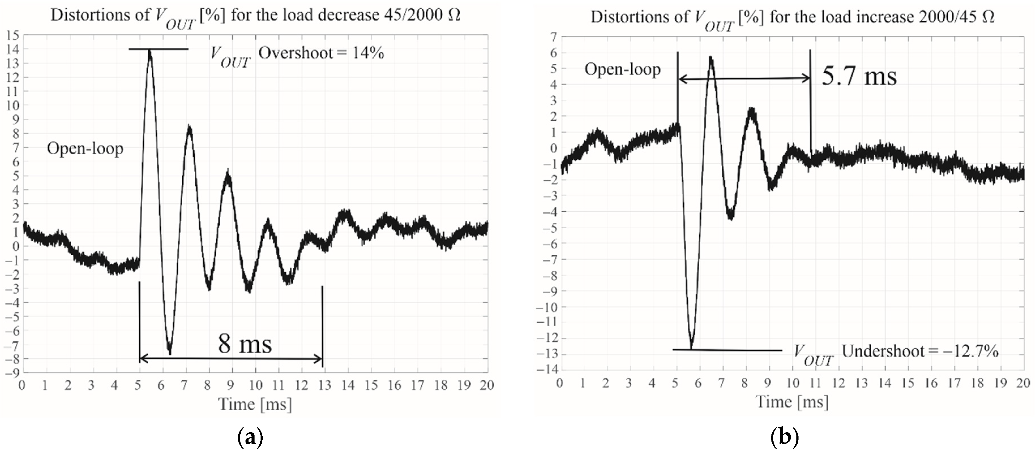
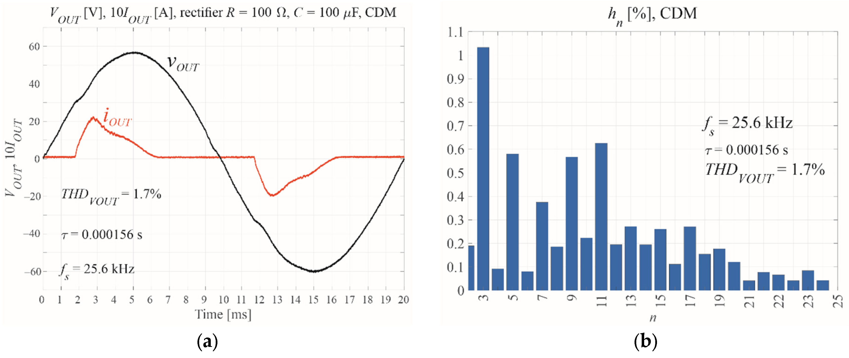
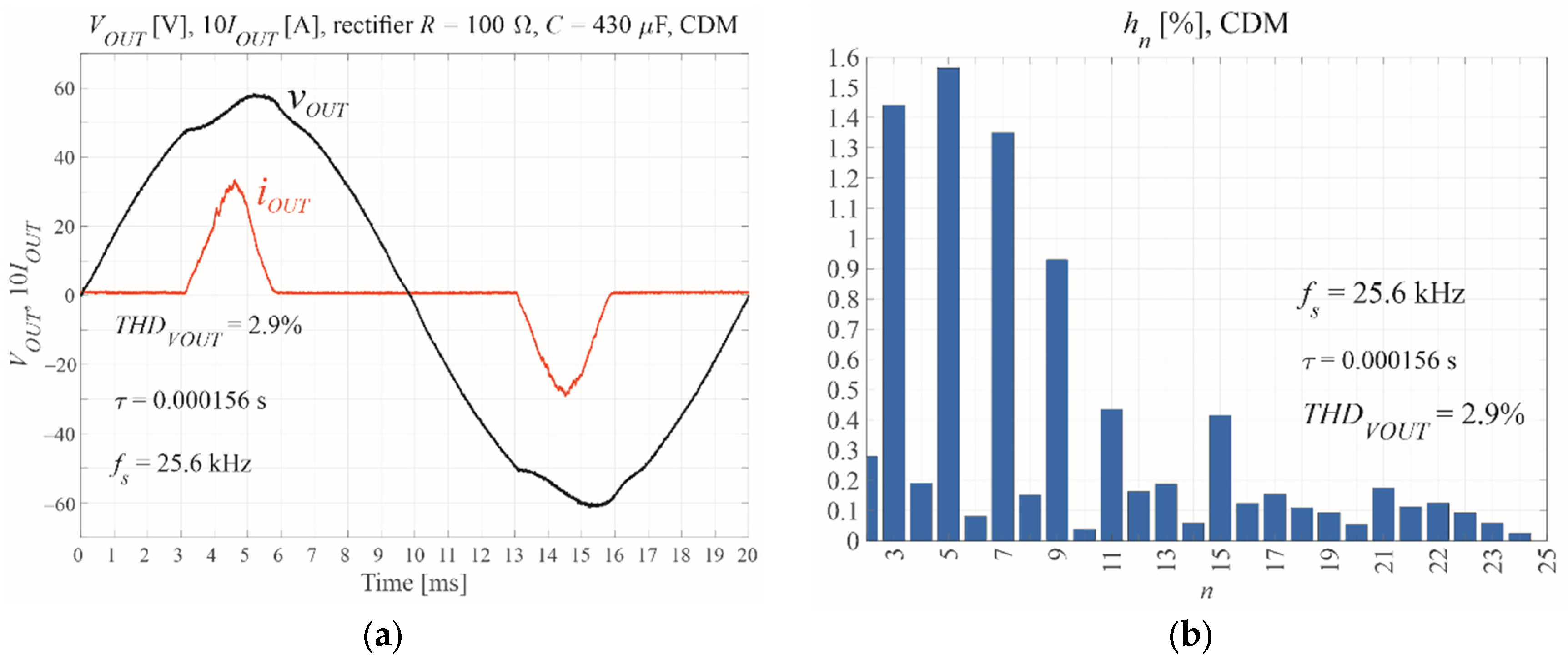
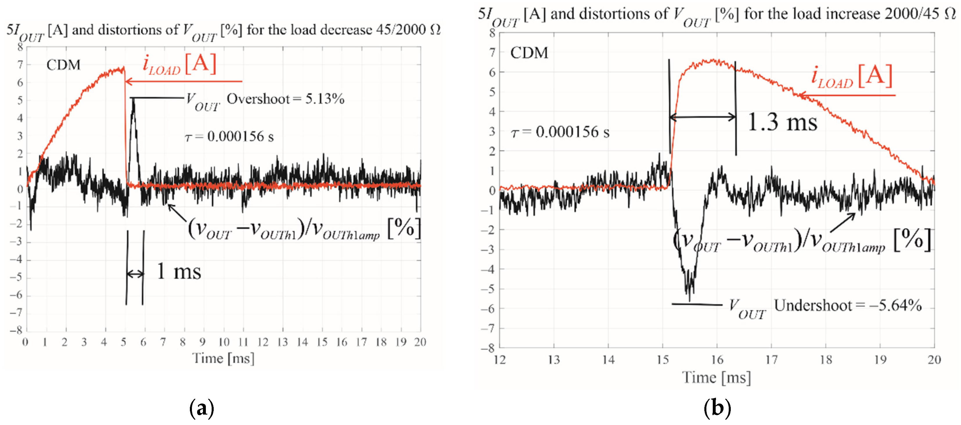
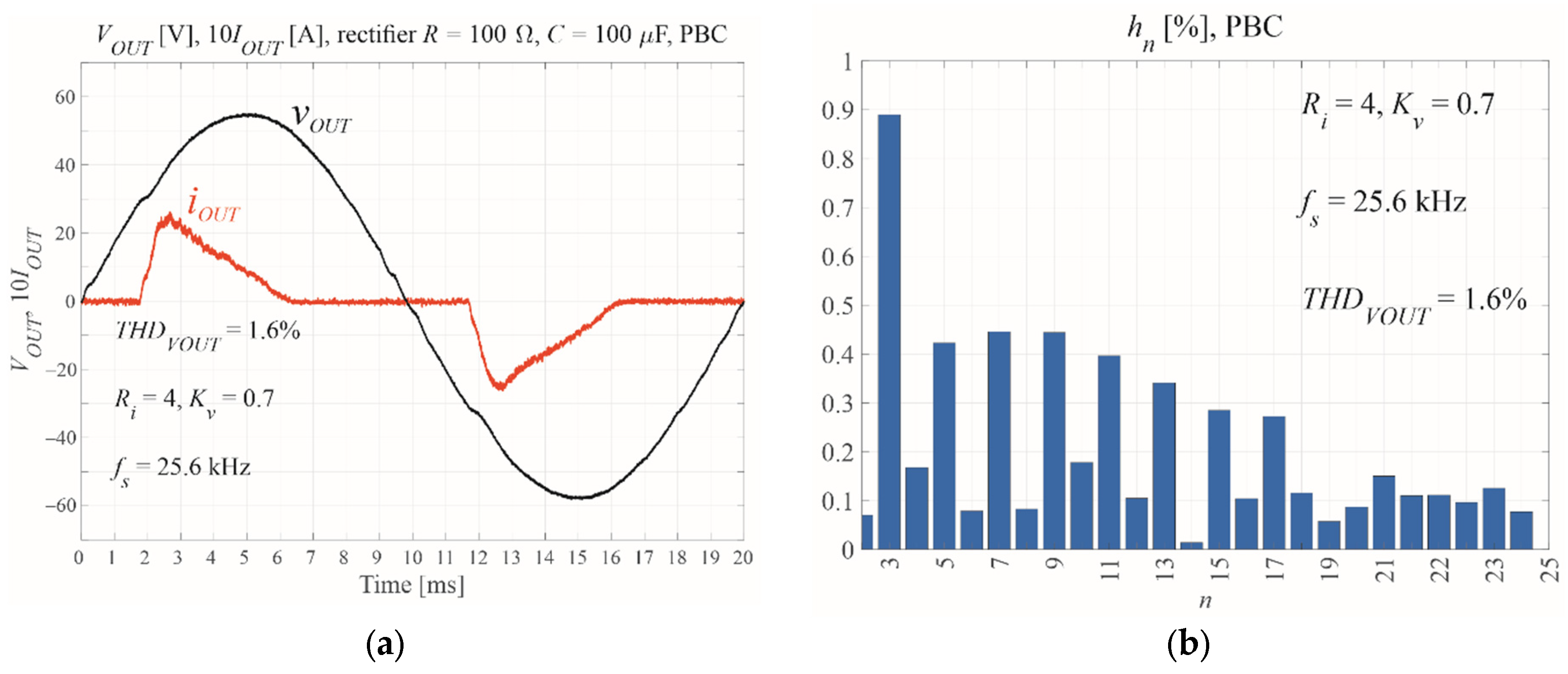
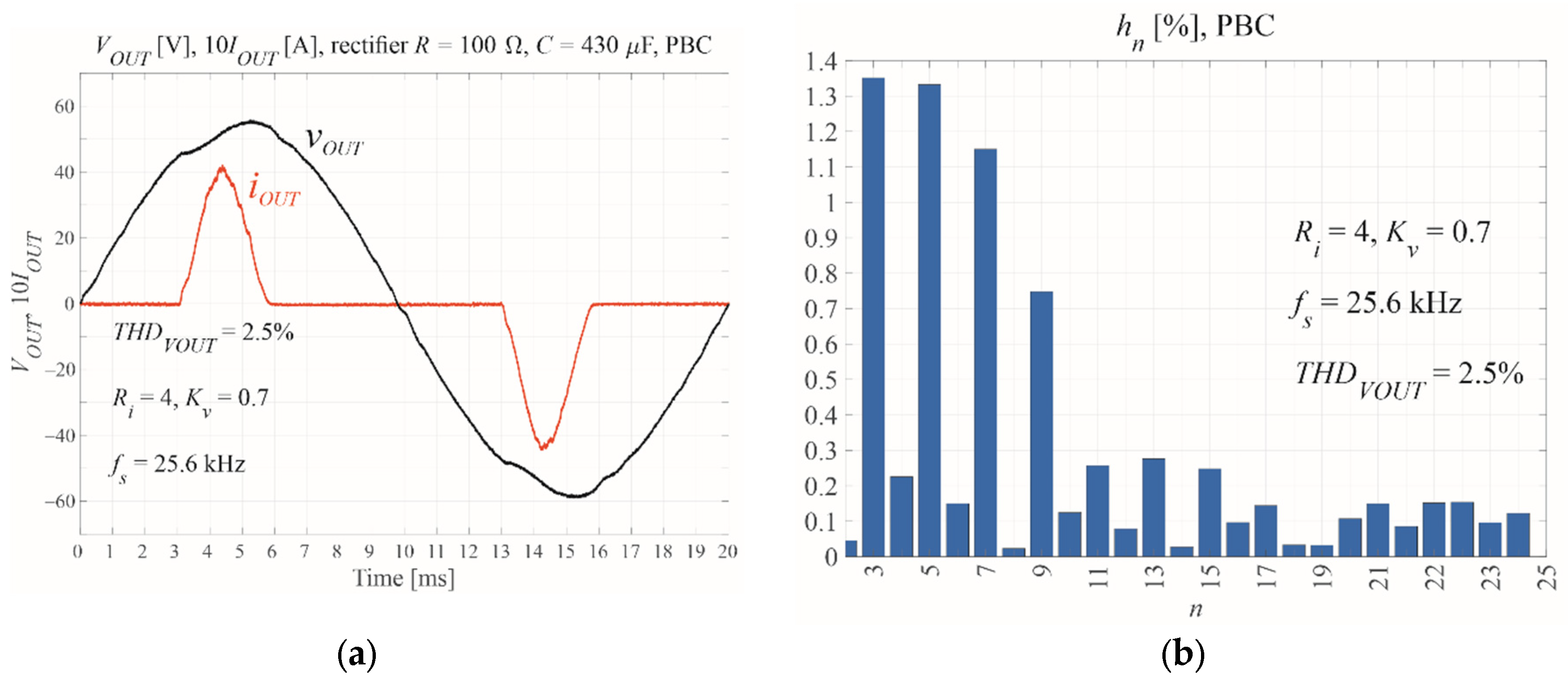
Figure 27 presents the output voltage and current waveforms (a) for the open-loop system, and (b) the output voltage harmonics spectrum for the rectifier R = 100 Ω, C = 100 µF load. Figure 28 presents compatible waveforms for the rectifier R = 100 Ω, C = 430 µF load. Figure 29 presents the distortions for the open-loop system, the step load decrease (45/2000 Ω), and the step load increase (2000/45 Ω) for M = 0.7. Figure 30, Figure 31 and Figure 32 present the same waveforms for the SISO-CDM control, and Figure 33, Figure 34 and Figure 35 for the MISO-PBC. Figure 36 presents a comparison of measured VSI output current waveforms for the rectifier RC load ((a) R = 100 Ω, C = 100 µF and (b) R = 100 Ω, C = 430 µF) for the open-loop, SISO-CDM control, and MISO-PBC. The output current slope is faster for MISO-PBC than for SISO-CDM, which results in lower output voltage distortions. However, the equivalent serial resistance in the experimental VSI was probably bigger than assigned in the simulation, and owing to this, the maximum values of measured currents are lower than in the simulation.

8. Discussion

The simulations and experimental verification of the control systems were performed for the harmonic disturbances (rectifier RC load resulting in PF = 0.7 for the open-loop system) and the dynamic resistive load. The final results can be compared in Table 3 (simulations) and Table 4 (experiments). The best simulated results were for MISO-OSAP, but it was very sensitive to the additional delay in measurement channels. The improvement of it with the prediction of the state variables by means of the Luenberger Observer worked properly for the harmonic disturbances, but was unsatisfactory for the dynamic load. So, OSAP was not experimentally tested. Among the two controls—the SISO-CDM and MISO-PBC—the MISO-PBC system resulted in lower THD of the output voltage for the nonlinear rectifier RC load, but had in experimental work slightly higher output voltage overshoots and undershoots, and slightly longer settling time for the dynamic load than the system with SISO-CDM. It can be explained that MISO-PBC calculates energy stored in the inverter, and SISO-CDM immediately responds to the output voltage change. The lower THD of the output voltage for the MISO-PBC is a result of the better shaping of the output current (both currents are at the inputs of the control system) than in the case of SISO-CDM—the output current (PBC) increases faster (Figure 36) to reduce the voltage drop after the rectifier begins to conduct. The energy delivered to the load in one fundamental period (20 ms) is the same with any feedback or without it, but feedback carves the output current shape, minimizing the distortions of the output voltage. The faster falling current in the case of the feedback reduces the distortions of the output voltage when the load rectifier stops conducting. The upper limit of the current slope increase is the restriction by the ratio of the voltage on the filter choke to its inductance value (for VDC = 85 V, M = 0.7, LF = 2 mH, equal to 17,300 A/s) when the rectifier begins conducting. Therefore, the lower the value of the modulation index M and the lower the value of the choke inductance LF, the higher the possibility of feedback increasing the current slope. In the experimental measurements for rectifier RC load 100 Ω || 100 µF, the slope of current (averaging the instantaneous distortions and for the almost linear part of the slope) for open-loop was about 1215 A/s, for CDM was about 2059A/s, and for PBC about 4974 A/s. For the rectifier RC load 100 Ω|| 430 µF, the slope of current for open-loop was about 1695 A/s, for CDM was about 2337A/s, and for PBC over 4579 A/s. The faster the increase in the output current, the lower the distortions caused by the nonlinear load. The maximum values of output currents for CDM and PBC and their slope increase are lower in the experimental VSI than in simulations. It causes a higher THD of the output voltage. One of the possible reasons can be a higher real equivalent serial resistance than assigned. In simulations, one constant value of this resistance was assigned. In the real device, it changes with the filter inductor magnetizing current, resulting from variable power losses in the coil core.

9. Conclusions

The price of the main control unit—the microprocessor with embedded analog-to-digital converters—is the same for all the feedback systems. However, the MISO controller requires three measurement channels (for the state variables: output voltage, inductor current, and output current), and the SISO controller has only one output voltage measurement channel. So, the MISO controller is more expensive. The SISO-CDM controller in the basic version (using the Standard Manabe Form) has simply calculated the coefficients of the closed-loop characteristic equation, and the only adjustment concerns the time constant of the closed-loop system. The design practice shows that it should be four or five switching periods (for fs = 25,600 Hz). We should adjust only one scaling factor of the output voltage measurement. In the case of MISO-PBC, we should adjust the two controller gains (voltage and current) within the allowable ranges. Additionally, we have to set three scaling factors in the voltage and both current measuring channels. The result of the reduction in the harmonic distortions for the nonlinear rectifier RC load (for Power Factor equal to 0.7) is better for MISO-PBC; for the more “trouble load”, the profit is higher, but the overshoots and undershoots for the dynamic load change are slightly higher for MISO-PBC than for SISO-CDM because the PBC idea is based on complex energy calculation, and SISO-CDM simply measures output voltage. Finally, it is hard to choose between the MISO-PBC and the SISO-CDM control—higher cost, lower distortions of the output voltage for the nonlinear load, versus a cheaper device and slightly better dynamics. The real improving parameters can be achieved by increasing switching frequency, e.g., up to 51,200 Hz [22], because it decreases the delays in the system and does not need any prediction of state variables, which can worsen the dynamic parameters of the control system (as in the case of the simulated MISO-OSAP-LO), but for the higher switching frequency the power losses increase. It would be possible to improve the control by further increasing the current slope (we have a margin to its highest possible value), but the problem could be with the stability of the system when the gains of the controller are higher.
The presented control systems of UPS fulfill the requirements of the best UPS classification class (“S”—sinusoidal mode) of IEC 62040-3:2021 [11] standard when THD of the output voltage should be below 8% for linear and nonlinear loads, and the limitation of the harmonics spectrum should be according to IEC 61000-2-2 standard [43].
The presented control systems of UPS fulfill the requirements of the first class of the transient performance [11] when over- and undershoot should be below 30% of the nominal voltage, and the settling time to 10% above or below the nominal output voltage should be below 100 ms for the defined step load changes.

Funding

The author was supported by a pro-quality grant from the Rector of the Silesian University of Technology, Zbigniew Rymarski, grant number: 02/140/RGJ26/0043. This research was partially supported by the Polish Ministry of Education and Science funding for statutory activities (BK-255/RAU11/2026).

Data Availability Statement

All data files with results of simulations and measurements, the software (MATLAB R2021b) for VSI simulation, and control (MDK-ARM, Professional Version 5) of the experimental inverter are available under licenses provided by our university. The data presented in this study are available on request from the author due to privacy concerns.

Acknowledgments

The author would like to thank Krzysztof Bernacki, Department of Electronics, Electrical Engineering and Microelectronics, Faculty of Automatic Control, Electronics and Computer Science, Silesian University of Technology, Gliwice, Poland, for his previous cooperation in inverter control research and his participation in the power electronics laboratory creation.

Conflicts of Interest

The author declares no conflicts of interest.

References

  1. Ben-Brahim, L.; Yokoyama, T.; Kawamura, A. Digital control for UPS inverters. In Proceedings of the Fifth International Conference on Power Electronics and Drive Systems, 2003, PEDS 2003, Singapore, 17–20 November 2003; Volume 2, pp. 1252–1257. [Google Scholar]
  2. Deng, H.; Srinivasan, D.; Oruganti, R. Modeling and control of single-phase UPS inverters: A survey. In Proceedings of the International Conference on Power Electronics and Drives Systems, 2005, PEDS 2005, Kuala Lumpur, Malaysia, 28 November–1 December 2005; pp. 848–853. [Google Scholar]
  3. Serra, F.M.; De Angelo, C.H.; Forchetti, D.G. IDA-PBC control of a DC–AC converter for sinusoidal three-phase voltage generation. Int. J. Electron. 2016, 104, 93–110. [Google Scholar] [CrossRef] [Scilit]
  4. Borsalani, J.; Dastfan, A. Decoupled phase voltages control of three phase four-leg voltage source inverter via state feedback. In Proceedings of the 2012 2nd International eConference on Computer and Knowledge Engineering (ICCKE), Mashhad, Iran, 18–19 October 2012; pp. 71–76. [Google Scholar] [CrossRef] [Scilit]
  5. Moon, S.; Choe, J.M.; Lai, J.S. Design of a state-space controller employing a deadbeat state observer for ups inverters. In Proceedings of the 2017 Asian Conference on Energy, Power and Transportation Electrification (ACEPT), Singapore, 24–26 October 2017; pp. 1–6. [Google Scholar] [CrossRef] [Scilit]
  6. Hu, C.; Wang, Y.; Luo, S.; Zhang, F. State-space model of an inverter-based micro-grid. In Proceedings of the 2018 3rd International Conference on Intelligent Green Building and Smart Grid (IGBSG), Yilan, Taiwan, 22–25 April 2018; pp. 1–7. [Google Scholar] [CrossRef] [Scilit]
  7. Rymarski, Z.; Bernacki, K. Different Features of Control Systems for Single-Phase Voltage Source Inverters. Energies 2020, 13, 4100. [Google Scholar] [CrossRef] [Scilit]
  8. Manabe, S. Coefficient diagram method. IFAC Proc. Vol. 1998, 31, 211–222. [Google Scholar] [CrossRef] [Scilit]
  9. Manabe, S. Importance of coefficient diagram in polynomial method. In Proceedings of the 42nd IEEE Conference on Decision and Control, Maui, HI, USA, 9–12 December 2003; pp. 3489–3494. [Google Scholar] [CrossRef] [Scilit]
  10. Coelho, J.P.; Pinho, T.M.; Boaventura-Cunha, J. Controller system design using the coefficient diagram method. Arab. J. Sci. Eng. 2016, 41, 3663–3681. [Google Scholar] [CrossRef] [Scilit]
  11. IEC 62040-3:2021; Uninterruptible Power Systems (UPS)—Part 3: Method of Specifying the Performance and Test Requirements. IEC: Geneva, Switzerland, 2021.
  12. Komurcugil, H. Improved passivity-based control method and its robustness analysis for single-phase uninterruptible power supply inverters. IET Power Electron. 2015, 8, 1558–1570. [Google Scholar] [CrossRef] [Scilit]
  13. Ortega, R.; Perez, J.A.L.; Nicklasson, P.J.; Sira-Ramirez, H. Passivity-Based Control of Euler-Lagrange Systems: Mechanical, Electrical and Electromechanical Applications (Communications and Control Engineering); Springer: London, UK, 1998. [Google Scholar]
  14. Wang, Z.; Goldsmith, P. Modified energy-balancing-based control for the tracking problem. IET Control Theory Appl. 2008, 2, 310–312. [Google Scholar] [CrossRef] [Scilit]
  15. Ortega, R.; Garcia-Canseco, E. Interconnection and Damping Assignment Passivity-Based Control: A Survey. Eur. J. Control 2004, 5, 432–450. [Google Scholar] [CrossRef] [Scilit]
  16. Ortega, R.; Garcia-Canseco, E. Interconnection and Damping Assignment Passivity-Based Control: Towards a Constructive Procedure—Part I. In Proceedings of the 43rd IEEE Conference on Decision and Control, Nassau, Bahamas, 14–17 December 2004; pp. 3412–3417. [Google Scholar] [CrossRef] [Scilit]
  17. Ortega, R.; Espinosa-Perez, G. Passivity-based control with simultaneous energy-shaping and damping injection: The induction motor case study. IFAC Proc. Vol. 2005, 38, 477–482. [Google Scholar] [CrossRef] [Scilit]
  18. Khefifi, N.; Houari, A.; Ait-Ahmed, M.; Machmoum, M.; Ghanes, M. Robust IDA-PBC based Load Voltage Controller for Power Quality Enhancement of Standalone Microgrids. In Proceedings of the IEEE IECON 2018—44th Annual Conference of the IEEE Industrial Electronics Society, Washington, DC, USA, 21–23 October 2018; pp. 249–254. [Google Scholar] [CrossRef] [Scilit]
  19. Kawamura, A.; Chuarayapratip, R.; Haneyoshi, T. Deadbeat control of PWM inverter with modified pulse patterns for uninterruptible power supply. IEEE Trans. Ind. Electron. 1988, 35, 295–300. [Google Scholar] [CrossRef]
  20. Milbradt, D.M.C.; Hollweg, G.V.; Paulo, E.; Barreto da Silveira, W.; Gründling, H. A robust adaptive One Sample Ahead Preview controller for grid-injected currents of a grid-tied power converter with an LCL filter. Int. J. Electr. Power Energy Syst. 2022, 142, 108286. [Google Scholar] [CrossRef] [Scilit]
  21. Rech, C.; Grundling, H.A.; Pinheiro, J.R. Comparison of discrete control techniques for UPS applications. In Conference Record of the 2000 IEEE Industry Applications Conference, Proceedings of the Thirty-Fifth IAS Annual Meeting and World Conference on Industrial Applications of Electrical Energy (Cat. No.00CH37129), Rome, Italy, 8–12 October 2000; IEEE: New York, NY, USA; Volume 4, pp. 2531–2537. [CrossRef] [Scilit]
  22. Rymarski, Z. The Influence of Switching Frequency on Control in Voltage Source Inverters. Energies 2024, 17, 4508. [Google Scholar] [CrossRef] [Scilit]
  23. Van der Broeck, H.W.; Miller, M. Harmonics in DC to AC converters of single-phase uninterruptible power supplies. In Proceedings of the 17th International Telecommunications Energy Conference 1995, INTELEC ‘95, The Hague, The Netherlands, 29 October–1 November 1995; pp. 653–658. [Google Scholar]
  24. Rymarski, Z. Single-Phase and Three-Phase Voltage Source Inverters Used in UPS Systems; Wydawnictwo Politechniki Śląskiej: Gliwice, Poland, 2010; ISBN 978-83-7335-642-9. [Google Scholar]
  25. Luo, F.L.; Ye, H.; Rashid, M.H. Digital Power Electronics and Applications; Academic Press: Cambridge, MA, USA, 2005. [Google Scholar]
  26. IEEE 519-2022; IEEE Standard for Harmonic Control in Electric Power Systems. IEEE: New York, NY, USA, 2022.
  27. Dahono, P.A.; Purwadi, A.; Qamaruzzaman. An LC filter design method for single-phase PWM inverters. In Proceedings of the International Conference on Power Electronics and Drive System, Singapore, 21–24 February 1995; Volume 2, pp. 571–576. [Google Scholar]
  28. Micrometals Alloy Powder Core Catalog. 2021. Available online: https://micrometals.com/design-and-applications/literature/ (accessed on 18 January 2026).
  29. Rymarski, Z. Measuring the real parameters of single-phase voltage source inverters for UPS systems. Int. J. Electron. 2017, 104, 1020–1033. [Google Scholar] [CrossRef] [Scilit]
  30. Rymarski, Z. The discrete model of the power stage of the voltage source inverter for UPS. Int. J. Electron. 2011, 98, 1291–1304. [Google Scholar] [CrossRef] [Scilit]
  31. Luenberger, D.G. Observing the state of a linear system. IEEE Trans. Mil. Electron. 1964, 8, 74–80. [Google Scholar] [CrossRef] [Scilit]
  32. Luenberger, D.G. An introduction to observers. IEEE Trans. Autom. Control 1971, 16, 596–602. [Google Scholar] [CrossRef] [Scilit]
  33. Davis, J.H. Luenberger Observers. In Foundations of Deterministic and Stochastic Control; Systems & Control: Foundations & Applications; Birkhäuser: Boston, MA, USA, 2002; pp. 245–254. [Google Scholar] [CrossRef] [Scilit]
  34. Mohammed, S.; Hani, B.; Aissa, C. Efficient Deadbeat Control of Single-Phase Inverter with Observer for High Performance Applications. Prz. Elektrotechniczny 2023, 99, 237–242. [Google Scholar] [CrossRef] [Scilit]
  35. Fan, H.; Li, Z.; Rodriguez, J.; Wang, B. Model Free Predictive Current Control for Voltage Source Inverter using Luenberger Observer. In Proceedings of the 2023 IEEE International Conference on Predictive Control of Electrical Drives and Power Electronics (PRECEDE), Wuhan, China, 16–19 June 2023; pp. 1–6. [Google Scholar] [CrossRef] [Scilit]
  36. Heydaridoostabad, H.; Ghazi, R. A new approach to design an observer for load current of UPS based on Fourier series theory in model predictive control system. Int. J. Electr. Power Energy Syst. 2018, 104, 898–909. [Google Scholar] [CrossRef] [Scilit]
  37. Li, J.; Sun, Y.; Li, X.; Xie, S.; Lin, J.; Su, M. Observer-Based Adaptive Control for Single-Phase UPS Inverter Under Nonlinear Load. IEEE Trans. Transp. Electrif. 2022, 8, 2785–2796. [Google Scholar] [CrossRef] [Scilit]
  38. Montagner, V.F.; Carati, E.G.; Grundling, H.A. An adaptive linear quadratic regulator with repetitive controller applied to uninterruptible power supplies. In Proceedings of the Industry Applications Conference 2000, Rome, Italy, 8–12 October 2000; Volume 4, pp. 2231–2236. [Google Scholar]
  39. Zuo, X.; Li, J.; Zhang, Z.; Man, T. The Passivity-based Control with Luenberger State Observer of Three-phase Grid Connected Converter. In Proceedings of the 2024 12th International Conference on Smart Grid and Clean Energy Technologies (ICSGCE), Jilin, China, 18–20 October 2024; pp. 1–7. [Google Scholar] [CrossRef] [Scilit]
  40. Bakhti, I.; Chaouch, S.; Makouf, A.; Douadi, T. Robust sensorless sliding mode control with Luenberger observer design applied to permanent magnet synchronous motor. In Proceedings of the 2016 5th International Conference on Systems and Control (ICSC), Marrakesh, Morocco, 25–27 May 2016; pp. 204–210. [Google Scholar] [CrossRef] [Scilit]
  41. Tietze, U.; Schenk, C. Electronic Circuits—Electronic Circuits: Handbook for Design and Applications, 2nd ed.; Springer: Berlin/Heidelberg, Germany, 2008; ISBN 978-3-540-00429-5. [Google Scholar]
  42. Bernacki, K.; Rymarski, Z. Contemporary Design Process for Single-Phase Voltage Source Inverter Control Systems. Sensors 2022, 22, 7211. [Google Scholar] [CrossRef] [Scilit] [PubMed]
  43. IEC 61000-2-2:2002+A1:2017+A2:2018; Electromagnetic Compatibility (EMC)—Part 2-2: Environment–Compatibility Levels for Low-Frequency Conducted Disturbances and Signalling in Public Low-Voltage Power Supply Systems. IEC: Geneva, Switzerland, 2018.
Figure 1. The block diagram of the simulated and tested VSI with the loads according to IEC 62040-3:2021.
Energies 19 01548 g001
Figure 2. Bode plots of the five output voltage measurement channels.
Energies 19 01548 g002
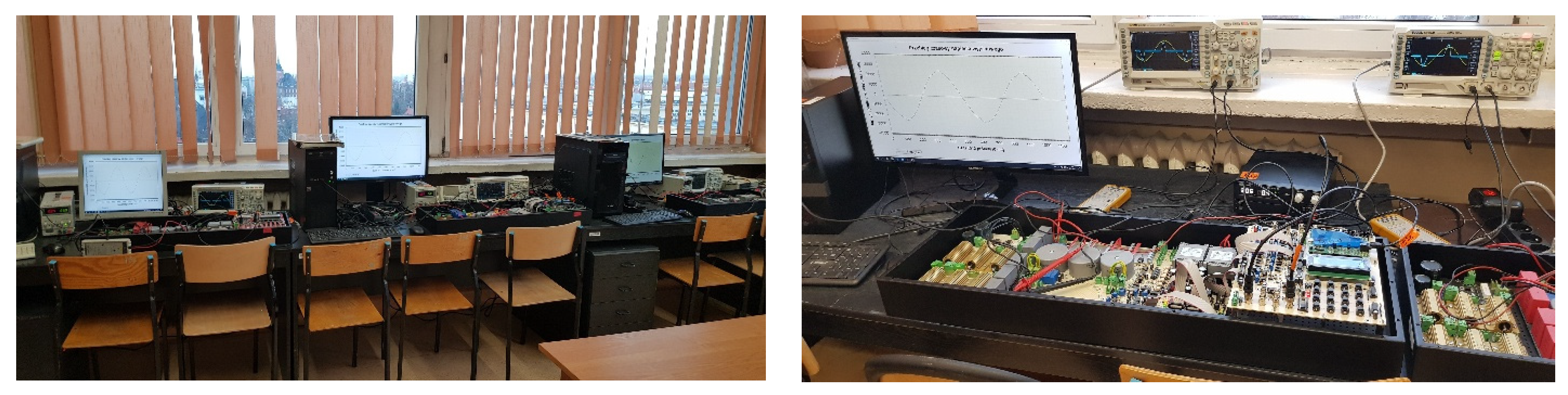
Figure 3. Laboratory with five measured inverters.
Energies 19 01548 g003
Figure 4. Block diagram of the SISO control.
Energies 19 01548 g004
Figure 5. Simulation model diagram of the VSI with CDM controller and the nonlinear RC load.
Energies 19 01548 g005
Figure 6. Simulation model diagram of the VSI with CDM controller and the dynamic load.
Energies 19 01548 g006
Figure 7. The simulation of distortions of the output voltage (a) for the open loop for the rectifier RC (100 Ω || 430 µF) and (b) the output voltage harmonics’ spectrum.
Energies 19 01548 g007
Figure 8. The simulation of distortions of the output voltage (a) for the SISO-CDM for the rectifier RC (100 Ω|| 430 µF) and (b) the output voltage harmonics’ spectrum.
Energies 19 01548 g008
Figure 9. The simulation of distortions for the open loop for (a) the step load decrease 45/500 Ω, and (b) for the step load increase 500/45 Ω.
Energies 19 01548 g009
Figure 10. The simulation of distortions for the SISO-CDM control for (a) the step load decrease 45/500 Ω, and (b) for the step load increase 500/45 Ω.
Energies 19 01548 g010
Figure 11. The control input signal VCTRL of the PWM modulator (simulation) for the SISO-CDM—the restriction of the modulation index M to omit modulator saturation: (a) for M = 0.7, there is no saturation; (b) for M = 0.8, there is a saturation of the modulator because its input signal limits are ±1.
Energies 19 01548 g011
Figure 12. The theoretically allowable areas of the current and voltage gains Ri and Kv of PBC for two values of the filter inductor (RL = 1 Ω, being much lower than Ri, has no serious influence on the plotted curves). The theoretically allowable gains are in the shaded areas. However, the values of the gains couples (signed with the crosses), tested in simulations, are lower than the calculated border. The values of the gains tested in the experimental VSI are in the circle.
Energies 19 01548 g012
Figure 13. The PBC controller realizes (40) and (41) control law equations.
Energies 19 01548 g013
Figure 14. The simulation diagram of VSI with the PBC controller from Figure 13 and the rectifier RC load (430 µF, 100 Ω).
Energies 19 01548 g014
Figure 15. The control voltage (simulation) for the different sets of gains, (a) Ri = 10 Ω and Kv = 0.2 S for the stable work, (b) Ri = 10 Ω and Kv = 0.3 S for oscillations (PBC is faster than PWM modulator speed).
Energies 19 01548 g015
Figure 16. The simulated distortions of the output voltage (a) for the PBC (Ri = 10 Ω and Kv = 0.2 S) for the rectifier RC load (100 Ω || 430 µF) and (b) the output voltage harmonics spectrum.
Energies 19 01548 g016
Figure 17. The simulation diagram of VSI with the PBC controller from Figure 13 for the dynamic load 45/500/45 Ω.
Energies 19 01548 g017
Figure 18. The simulated distortions for the PBC for (a) the step load decrease 45/500 Ω, and (b) for the step load increase 500/45 Ω.

Energies 19 01548 g018
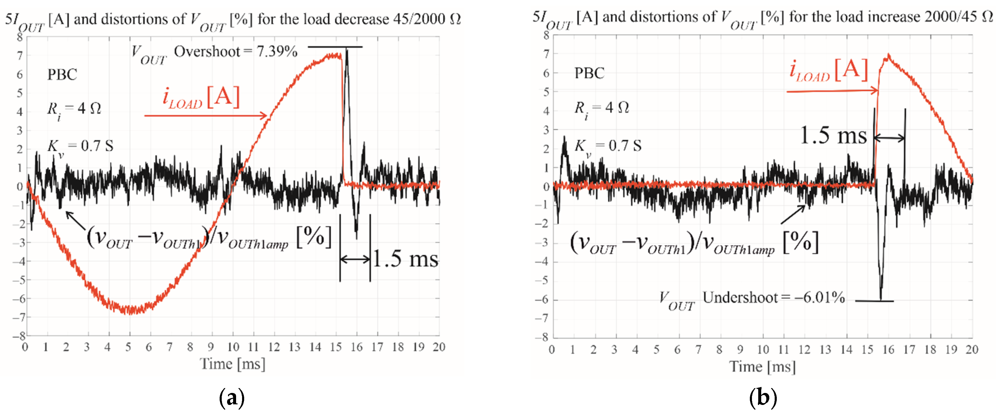
Figure 19. The simulation module diagram of VSI with the MISO-OSAP controller and the rectifier RC load (430 µF|| 100 Ω) without additional delays in the measurement channels.
Energies 19 01548 g019
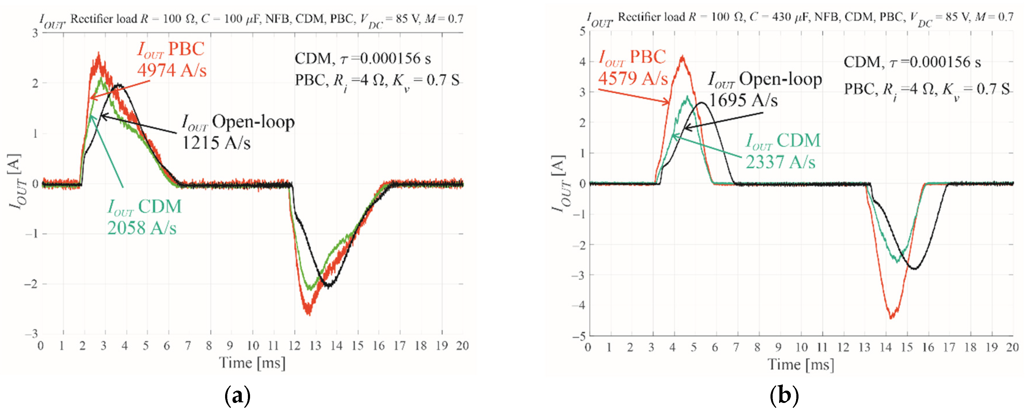
Figure 20. The simulated distortions of the output voltage, output current, and control voltage for the MISO-OSAP for the rectifier RC (100 Ω || 430 µF) (a) for M = 0.7 and (b) for M = 0.4.
Energies 19 01548 g020
Figure 21. The simulated distortions for the MISO-OSAP for the step load decrease 45/500 Ω, and for the step load increase 500/45 Ω for M = 0.7.
Energies 19 01548 g021
Figure 22. The maximum absolute values of the roots of (52) with the Luenberger gains lvOUT and liLF as parameters for fs = 25,600 Hz, LF = 2 mH, RF = 1 Ω, CF = 51 μF.
Energies 19 01548 g022
Figure 23. The simulation diagram of VSI with the MISO-OSAP-LO controller and the rectifier RC load (430 µF || 100 Ω) with additional delays 2Ts in the measurement channels.
Energies 19 01548 g023
Figure 24. The simulated distortions of (a) the output voltage for the MISO-OSAP-LO control for the rectifier RC and (b) the output voltage harmonics’ spectrum.
Energies 19 01548 g024
Figure 25. The simulated distortions for the MISO-OSAP-LO control for the step load decrease 45/500 Ω, and for the step load increase 500/45 Ω for M = 0.7.
Energies 19 01548 g025
Figure 26. The VSI (VDC = 85 V, M = 0.7, R = 100 Ω, C = 430 µF, LF = 0.002 H, CF = 51 µF) simulated output current and voltage for the rectifier RC load for the open-loop, SISO-CDM control, MISO-PBC, and MISO-OSAP (in this case, without additional delays in the measurement channels).
Energies 19 01548 g026
Figure 27. The measured (a) output voltage and current waveforms and (b) the output voltage harmonics spectrum for rectifier R = 100 Ω, C = 100 µF load, for the open loop.
Energies 19 01548 g027
Figure 28. The measured (a) output voltage and current waveforms and (b) the output voltage harmonics spectrum for rectifier R = 100 Ω, C = 430 µF load, for the open loop.
Energies 19 01548 g028
Figure 29. The measured distortions for the open-loop system during (a) a step load decrease (45/2000 Ω) and (b) a step load increase (2000/45 Ω) for M = 0.7.
Energies 19 01548 g029
Figure 30. The measured (a) output voltage and current waveforms and (b) the output voltage harmonics spectrum for rectifier R = 100 Ω, C = 100 µF load, for the CDM control.
Energies 19 01548 g030
Figure 31. The measured (a) output voltage and current waveforms and (b) the output voltage harmonics spectrum for rectifier R = 100 Ω, C = 430 µF load, for the CDM control.
Energies 19 01548 g031
Figure 32. The measured distortions for the CDM control during (a) a step load decrease (45/2000 Ω) and (b) a step load increase (2000/45 Ω) for M = 0.7.
Energies 19 01548 g032
Figure 33. The measured (a) output voltage and current waveforms and (b) the output voltage harmonics spectrum for rectifier R = 100 Ω, C = 100 µF load, for the PBC.
Energies 19 01548 g033
Figure 34. The measured (a) output voltage and current waveforms and (b) the output voltage harmonics spectrum for rectifier R = 100 Ω, C = 430 µF load, for the PBC.
Energies 19 01548 g034
Figure 35. The measured distortions for the PBC during (a) a step load decrease (45/2000 Ω) and (b) a step load increase (2000/45 Ω) for M = 0.7.
Energies 19 01548 g035
Figure 36. Comparison of the measured VSI output current waveforms for the rectifier RC load for the open-loop, SISO-CDM control, and MISO-PBC (VDC = 85 V, M = 0.7, R = 100 Ω, LF = 0.002 H, CF = 51 µF) (a) C = 100 µF, (b) C = 430 µF.
Energies 19 01548 g036
Table 1. Coefficients of the discretized Standard Manabe Form for τ = 4/25,600 s and τ = 5/25,600 s.
τpz0pz1pz2pz3pz4pz5
4/fs1−1.3270.6811−0.18260.0381−0.006738
5/fs1−1.78081.2885−0.50770.1272−0.0183
Table 2. Coefficients of the discretized CDM controller from Figure 4 for fs = 25,600 Hz, τ = 4/fs or 5/fs.
τLF, CFr0r1r2s0s1s2t0
4/fs1 mH, 51 µF10.59070.422430.1770−24.7324−0.46976.9871
4/fs2 mH, 51 µF10.62410.446465.6919−53.0062−0.925313.8305
5/fs1 mH, 51 µF10.13650.355816.8256−13.2966−1.27693.7438
5/fs2 mH, 51 µF10.17000.373737.9021−29.5197−251517.4106
Table 3. The comparison of the different simulated control results for the rectifier RC load and the dynamic load.
No FeedbackSISO_CDMMISO-PBCMISO-OSAPMISO-OSAPMISO-OSAP-LO
Delay of the measurement channel-------d = 2Tsd = 2Tsd = 0d = 2Tsd = 2Ts
THDVOUT for
RC load 100 Ω || 430 µF/
IOUT slope
6.78%/
1452 A/s
1,42%/
4218 A/s
0.83%/
7454 A/s
0.85%/
14,296 A/s
oscillations1.07%/
5464 A/s
Overshoot for
45/500 Ω
11.89%5.37%4.81%1.08%oscillations6.94%
Undershoot for
500/45 Ω
−10.52%−5.48%−5.47%−2.39%oscillations−25.77%
Settling time for 45/500 Ω14 ms4 ms3 ms0.3 msoscillations5.7 ms
Settling time for 500/45 Ω9 ms3.5 ms2.5 ms0.3 msoscillations5.7 ms
Table 4. The comparison of the different control results of the experimental VSI for the rectifier RC load and the dynamic load.
No FeedbackSISO-CDMMISO-PBC
THDVOUT [%] for RC rectifier load 100 Ω || 100 µF
/slope of the output current [A/s]
4.2%/1215 A/s1.7%/2059 A/s1.6%/4974 A/s
THDVOUT [%] for RC rectifier load 100 Ω || 430 µF
/slope of the output current [A/s]
6.6%/1695 A/s2.9%/2337 A/s2.5%/4579 A/s
Overshoot for 45/2000 Ω14%5.13%7.39%
Undershoot for 2000/45 Ω−12.7%−5.64%−6.01%
Settling time for the load decrease of 45/2000 Ω8 ms1 ms1.5 ms
Settling time for the load increase of 2000/45 Ω5.7 ms1.3 ms1.5 ms
Disclaimer/Publisher’s Note: The statements, opinions and data contained in all publications are solely those of the individual author(s) and contributor(s) and not of MDPI and/or the editor(s). MDPI and/or the editor(s) disclaim responsibility for any injury to people or property resulting from any ideas, methods, instructions or products referred to in the content.