1. Introduction
The 10 kV cable intermediate joint is a key component in the power cable system, primarily used to connect two sections of cable or repair damaged parts, ensuring the continuity and reliability of power transmission [
1]. The cable intermediate joint has a multi-layer composite insulation structure. Due to the compact design and the complex manufacturing and installation processes, defects of varying degrees are likely to occur within the insulation layers. Since the dielectric strength that each layer in the multi-layer composite insulation structure can withstand is proportional to the corresponding electrical strength, once the field strength exceeds the tolerance of a given dielectric layer, that layer will break down, and it can easily lead to breakdown of other dielectric layers [
2]. In non-uniform electric fields or under small overvoltage conditions, a “cumulative effect” will occur, causing a decrease in the breakdown voltage of solid dielectric materials, which then leads to partial discharge. Over time, this can lead to the degradation of the insulation performance of the intermediate joint, and in severe cases, it can cause insulation breakdown [
3,
4,
5]. Therefore, using non-destructive testing (NDT) technology to detect and evaluate defects in cable intermediate joints is of great importance [
6].
Currently, the main non-destructive testing methods for detecting defects in cable intermediate joints include partial discharge detection, ultrasonic testing, infrared imaging detection, X-ray/CT testing, and acoustic detection [
7,
8,
9,
10,
11,
12,
13,
14,
15,
16,
17]. Partial discharge detection assesses the insulation condition by monitoring partial discharge signals from the cable intermediate joint under high voltage. However, it is susceptible to electromagnetic interference and requires shielding to block environmental noise [
8,
9,
10,
11,
12]; ultrasonic testing detects internal defects or interface pressure changes by analyzing the propagation characteristics of ultrasonic waves in materials (reflection, refraction, attenuation, etc.). It requires coupling agents (such as glycerin) to transmit ultrasonic waves and cannot be used in a vacuum [
13,
14]; infrared imaging detection identifies local overheating or insulation degradation areas by measuring the temperature distribution on the surface of the cable intermediate joint. However, it is sensitive to environmental temperature and radiation interference, and can only detect surface or near-surface defects, being insensitive to deep defects [
15]; X-ray/CT testing uses X-rays to penetrate materials and analyzes internal structural defects through imaging. However, the equipment is costly, and there is a risk of radiation exposure, requiring strict safety precautions. It also has low sensitivity for materials with small density differences (such as rubber–polyethylene interfaces) [
16]; acoustic detection analyzes fault characteristics by collecting sound signals (such as discharges and mechanical vibrations) from cable accessories during operation. However, environmental noise can affect the accuracy of detection [
17]. In summary, there is an urgent need for a method capable of identifying and detecting defects inside cable joints.
Microwave testing technology, as a new non-destructive testing method, has the advantages of high sensitivity to non-metallic materials, non-contact detection, no coupling agents required, high resolution, and adjustable safety [
18,
19,
20]. Currently, there has been a large amount of research on microwave non-destructive testing technology worldwide, but research on its application to cable intermediate joint detection is still limited. Wang Xujie et al. proposed a method for detecting steel rebar corrosion in reinforced concrete structures based on microwave reflection. They used CST Studio Suite 2021 3D electromagnetic simulation software to establish a numerical simulation model of corrosion in reinforced concrete structures. By analyzing the changes in echo loss, they revealed the impact of different corrosion degrees on microwave testing results [
21]. Wang Liming et al. used the reflection characteristics of microwaves at the interface between different insulation layers to detect defects. They conducted experiments using flat samples and studied the relationship between defect size and detection accuracy. In the experiments, defects as small as 0.3 mm deep and 4 mm wide within the flat sample were detectable [
22,
23].
This paper proposes a microwave non-destructive testing method for detecting defects in 10 kV distribution cable intermediate joints. It uses simulation models to detect defects of different depths and types in intermediate joints, and experimental results are provided to verify the effectiveness of the proposed method in detecting defects in intermediate joints.
2. Model Construction
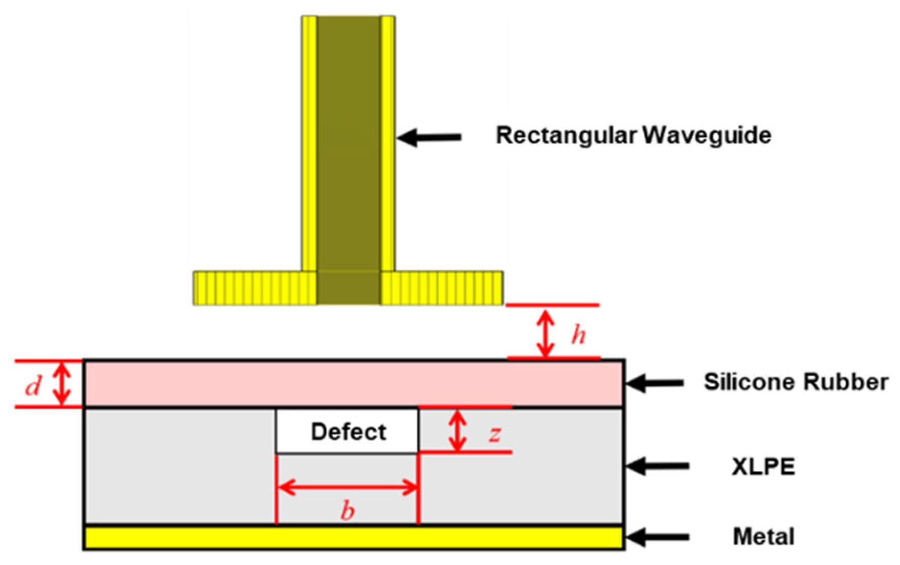
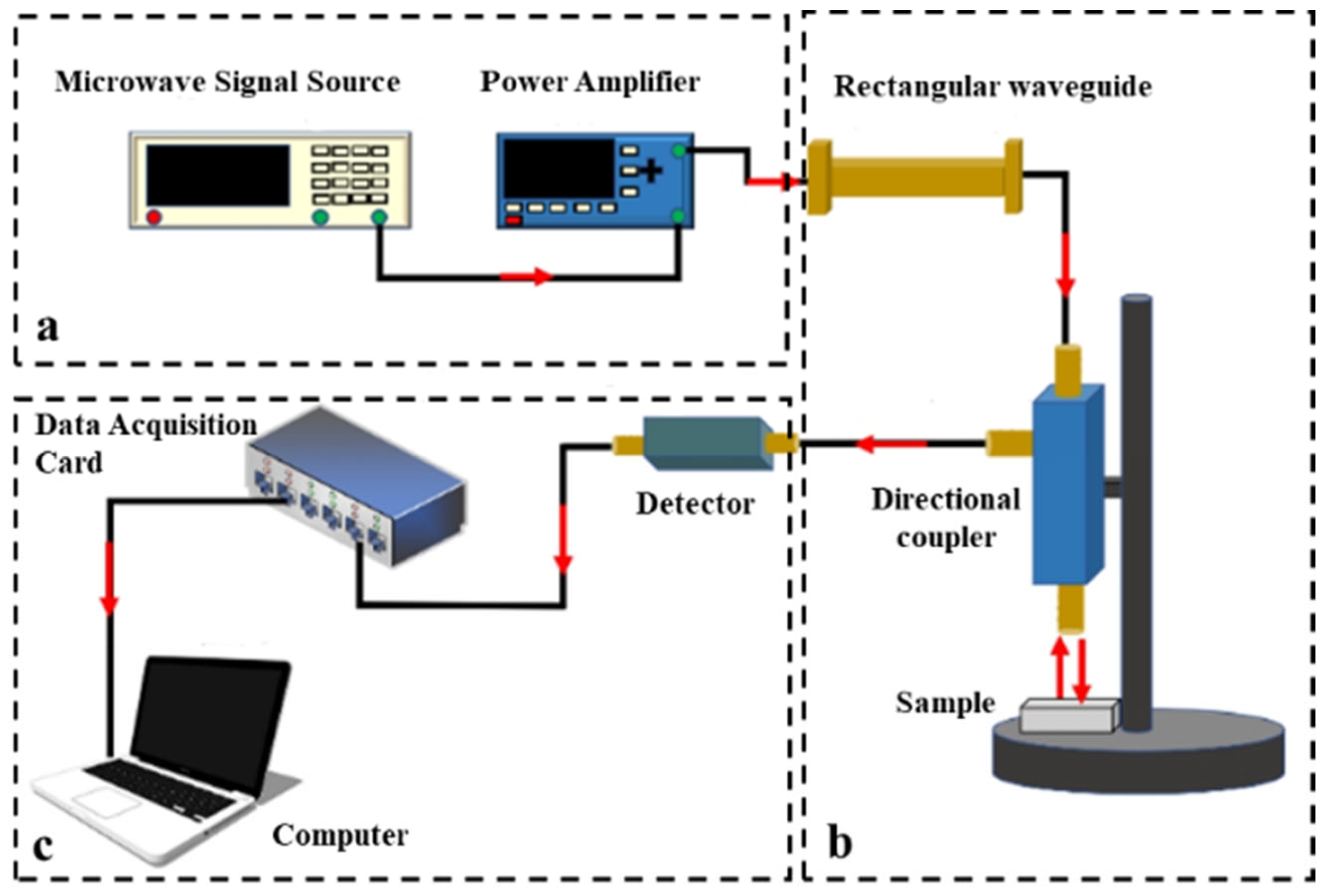
This paper uses the wave impedance model to calculate the reflection coefficient. The process of microwave inspection of the intermediate joint is simplified into the structure shown in
Figure 1.
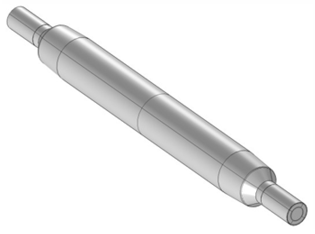
The intermediate joint is simplified into a planar structure consisting of a silicone rubber layer, a cross-linked polyethylene (XLPE) layer, and a metal layer. The detection probe is a metal waveguide with a rectangular cross-section. The dielectric constant ε, magnetic permeability μ, and thickness d of each layer of the medium are considered.
The wave impedance characterizes the ability of a medium to propagate electromagnetic waves. The reflection and refraction coefficients at the interface between two media can be calculated from the wave impedances of the two media. According to transmission line theory, for two planar media, the transmission line can be equivalently represented by a single new medium, and the new wave impedance is defined as the equivalent wave impedance.
Here,
k is the wave number. A phase change of 2π in space corresponds to one full wave, and
k represents the number of full waves per unit length.
μ and
ε are the magnetic permeability and dielectric constant of the medium.
D is the thickness of the incident medium;
η1 and
η2 are the wave impedances of the materials on the incident and transmission sides of the medium, respectively.
For multi-layer media, the bottom two layers of the medium are equivalently represented as a single wave impedance, effectively reducing the total number of medium layers by one. In other words, by repeatedly using Formula (1) and calculating from the transmission end to the incident end, the overall wave impedance can be obtained.
A rectangular waveguide is also a type of transmission line for electromagnetic waves, and its wave impedance is [
24]:
where a and b are the length and width of the cross-section of the rectangular waveguide, and λ is the operating microwave wavelength.
According to the wave impedance theory, the waveguide and the test sample are considered as two separate transmission lines. The reflection coefficient R at their interface is:
By calculating with Formula (5), it can be observed that when there is a defect in the intermediate joint (such as air gaps, the presence of conductive impurities, or moisture), the reflection coefficient of the microwaves at the interface between the waveguide probe and the intermediate joint will change significantly. This, in turn, causes a noticeable variation in the reflected signal. Based on this principle, internal defects in the intermediate joint can be detected by monitoring changes in the reflected signal’s amplitude.
5. Experimental Results and Discussion
5.1. Selection of the Optimal Detection Frequency
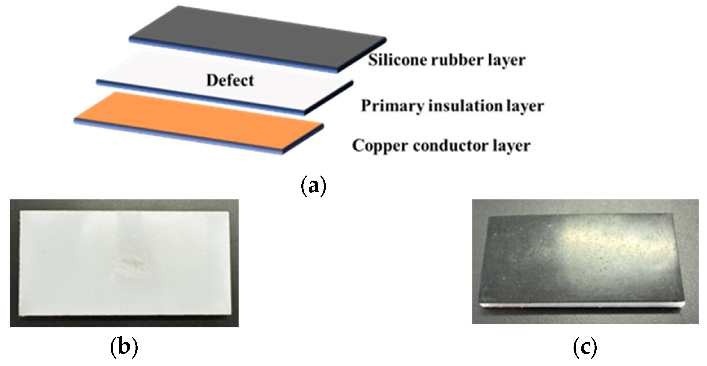
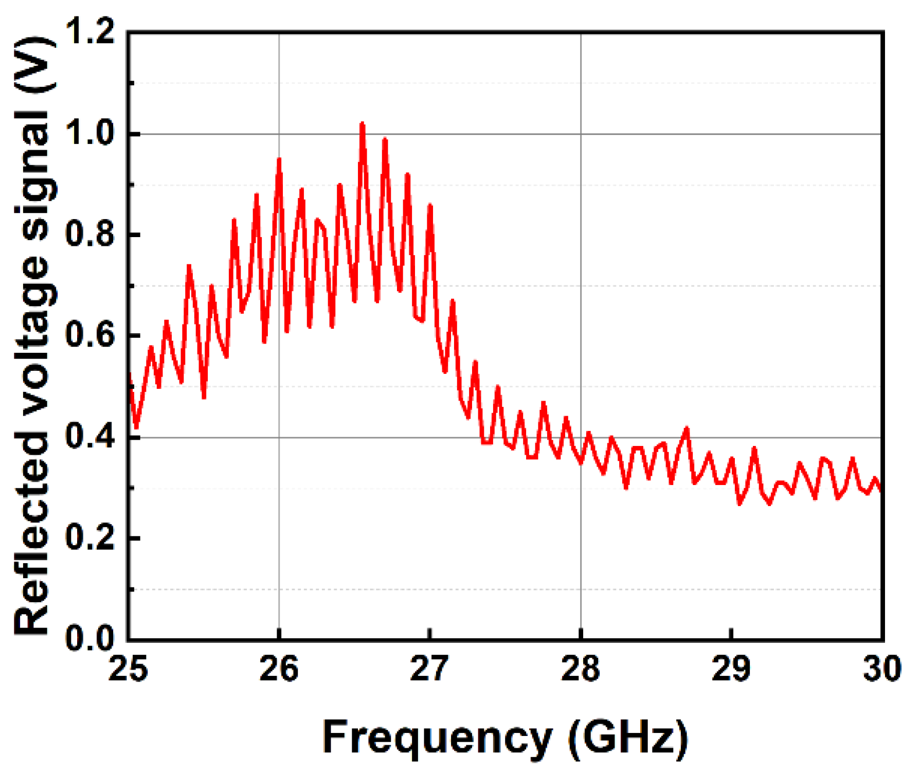
The microwave signal source is adjustable within the frequency range of 25 GHz to 30 GHz. To achieve the best detection results, it is necessary to determine the reflected voltage signal from the sample at different frequencies, and then select the frequency corresponding to the optimal reflected voltage signal for subsequent experiments. A flat sample with a thickness of 3 mm for silicone rubber, 5 mm for XLPE, and 1 mm for copper sheet was selected for the experiment. The reflected voltage signals at different frequencies are shown in
Figure 9.
It can be observed that the reflected voltage signal fluctuates with changes in frequency. This is due to the interference effect between the incident wave and the reflected wave generated at the points of impedance discontinuity within the system. The result of this interference is strongly dependent on the phase relationship between the two, with the phase difference being determined by both the propagation path length and the signal wavelength. When scanning the frequency, the change in wavelength leads to a continuous alteration of the phase difference, causing the interference state to periodically alternate between constructive and destructive interference. This ultimately results in a periodic fluctuation of the reflected signal in the frequency domain. At a frequency of 26.55 GHz, the reflected voltage signal reaches its maximum value of 1.05 V; thus this frequency is selected as the optimal detection frequency for subsequent experiments.
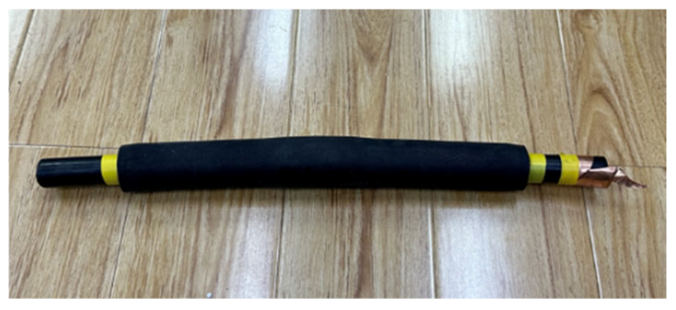
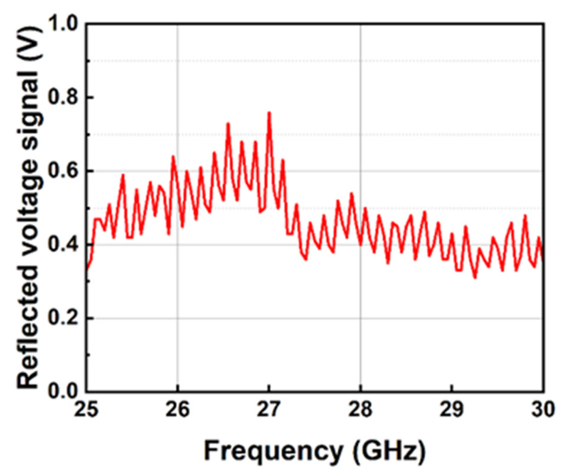
To maintain consistency with the actual intermediate joint, a 10 kV XLPE distribution cable cold-shrink-type intermediate joint was selected for the experiment. The reflected voltage signals at different frequencies are shown in
Figure 10.
It can be observed that the trend of the reflected voltage signal is similar to that of the flat sample, but the reflected voltage signal is smaller compared to the flat sample. This is due to the cylindrical shape of the cold-shrink-type intermediate joint, the incomplete fit between the rectangular waveguide port and the sample, and the structural characteristics of the sample. The maximum reflected voltage signal occurs at 27 GHz, with a value of 0.73 V. This frequency is selected as the optimal detection frequency for the cold-shrink-type intermediate joint sample in subsequent experiments.
5.2. The Reflected Signals of Different Defects
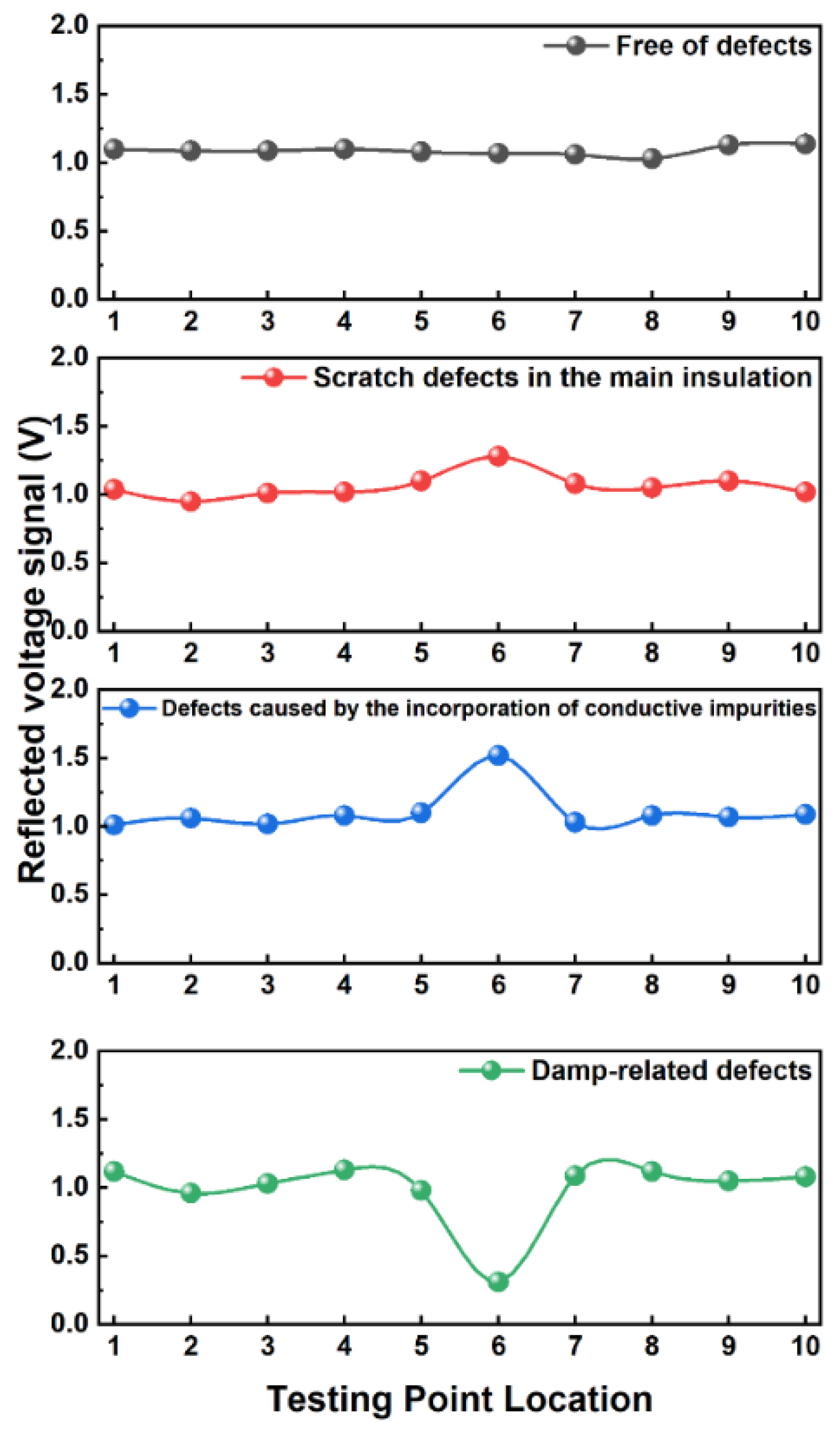
For the flat sample, microwave testing was first conducted on the pre-fabricated main insulation scratch defect, copper conductor impurity defect, and moisture defect. The test results are shown in
Figure 11.
As shown in the figure, between detection points 1–10, the curves remain stable overall, with a noticeable change occurring only near detection point 6. In the absence of defects, the reflected signal is stable around 1.1 V, indicating low system noise and minimal signal fluctuation. For the main insulation scratch defect, there is a slight increase near detection point 6, reaching a peak of 1.32 V. The moisture defect shows a significant reflection attenuation at the same position, with the signal dropping to 0.23 V. The conductive impurity defect, on the other hand, exhibits the most prominent reflection peak, with an amplitude of 1.52 V.
It can be seen that different defect types have a significant impact on the reflected voltage signal: the conductive impurity defect causes the most severe impedance change, leading to a strong reflection signal; the moisture defect results in a weaker reflection signal due to increased dielectric polarization loss; while the main insulation scratch defect causes relatively minor impedance disturbance, resulting in a less noticeable reflection response.
Therefore, the reflection signal amplitude characteristics can be used to distinguish different types of defects, with the conductive impurity defect producing the strongest reflection signal, making it most sensitive to microwave reflection detection. The abnormal signal change at detection point 6 indicates the presence of a defect in that location, which can be used for pinpointing defect identification and type judgment in cables.
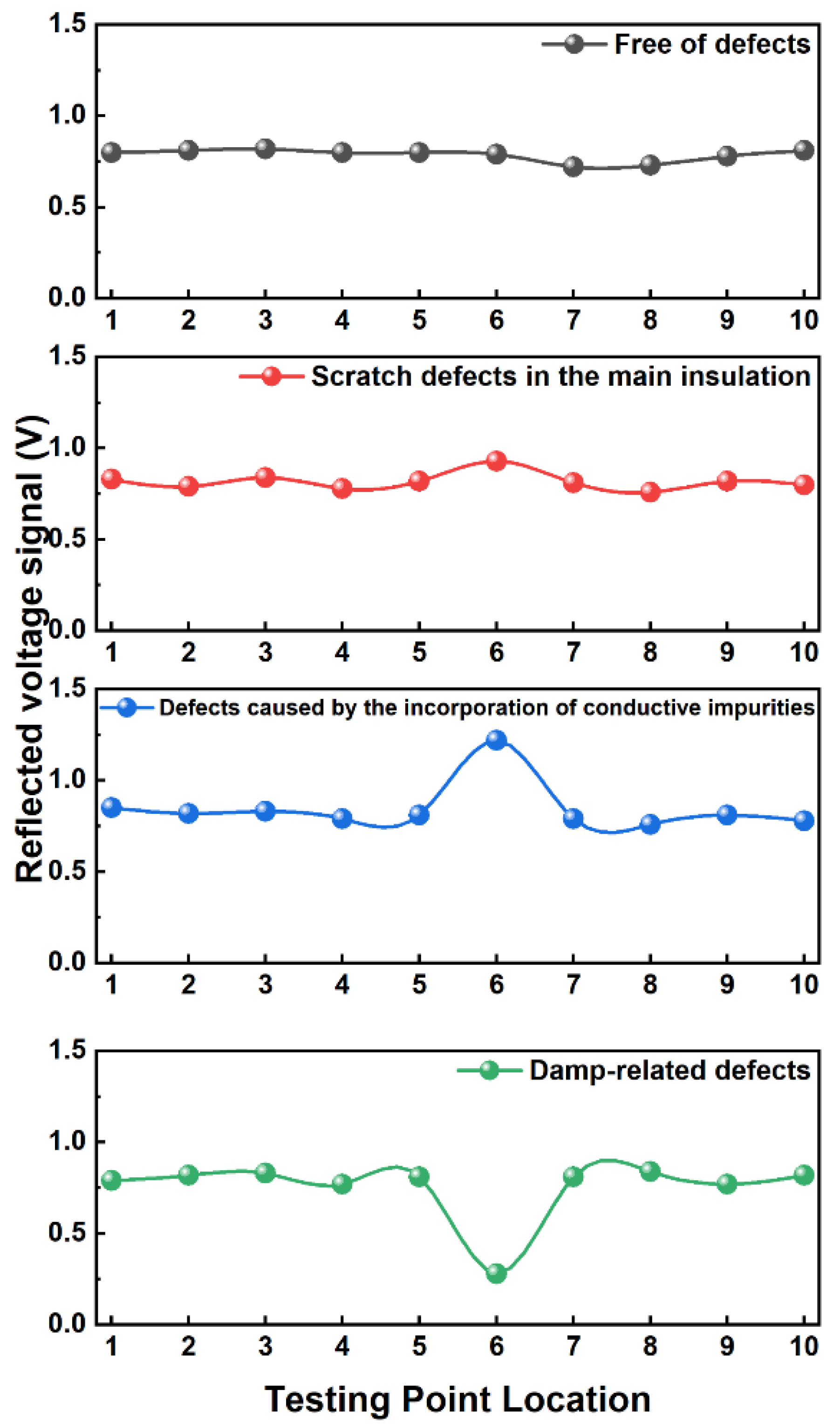
Next, defects similar to those in the flat sample were prefabricated in the cold-shrink intermediate joint sample, and the detection results are shown in
Figure 12.
Compared to the flat sample, the reflected signal amplitudes in the cold-shrink intermediate joint sample are generally lower, with a reduced fluctuation range. This is due to the more complex structure of the intermediate joint, with multiple layers of dielectric materials. When microwaves propagate through these multi-layer dielectrics, they undergo multiple reflections and attenuations, which weakens the strength of the reflected signals. However, the variation trends are consistent between the two samples: different defect types show significant differences around detection point 6, with the conductive impurity defect having the largest reflection signal and the moisture defect showing the weakest reflection signal.
In conclusion, the microwave reflection method demonstrates good consistency between the detection results in both the flat sample and the cold-shrink intermediate joint sample. This verifies the feasibility and accuracy of the method in real cable joint structures, enabling precise defect localization and type identification.
5.3. Extraction and Analysis of Microwave Detection Signals
Due to the inability to ensure uniformity in material and thickness for each sample, and the difficulty in accurately controlling the detection distance and angle during the experiment, small variations may occur. Therefore, it is necessary to first calculate the system error for the defect-free flat sample and the defect-free cold-shrink intermediate joint sample. The system error
Ue is the difference between the maximum and minimum values of the reflection voltage for the defect-free sample, as shown in expression (7). By comparing the actual measurement results with the system error, the internal defects of the cable terminal can be more accurately identified.
To more accurately identify defects, the reflection voltage signal
Ui obtained from the detection is subtracted by the average reflection voltage
U of the defect-free sample, resulting in the reflection voltage difference ΔU. The ratio of the reflection voltage difference Δ
U to the system error
Ue of the defect-free sample is then calculated, denoted as the relative value of the reflection voltage difference
Pi, as shown in expression (8). If
Pi > 100%, it indicates that the reflection voltage difference exceeds the system error by more than one time, which is reflected as a noticeable change in the detection curve, allowing for effective determination of the presence of a defect.
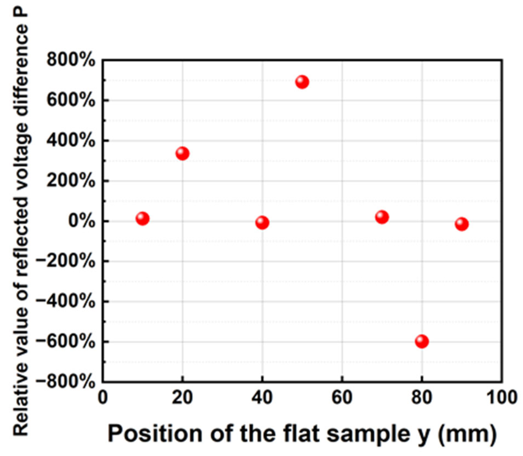
Three types of defects were pre-fabricated in the XLPE layer of the same flat sample. The length of the flat sample is 100 mm, denoted as y. At y = 20 mm, a main insulation scratch defect was pre-fabricated; at y = 50 mm, a conductive impurity defect was introduced; and at y = 80 mm, a moisture defect was created. Based on the relative value of the reflection voltage difference, the defect types were evaluated, and the results are shown in
Figure 13.
As shown in
Figure 13, when three typical defects—main insulation scratch, conductive impurity, and moisture—were pre-fabricated in the XLPE layer of the same flat sample, the relative reflection voltage values P exhibited significant differences at different positions. Among them, the conductive impurity defect at y = 50 mm had the highest relative reflection voltage value, approximately +700%, indicating that the presence of conductive impurities significantly altered the electromagnetic properties of the local medium, resulting in the most noticeable impedance mismatch and the highest reflection energy. The main insulation scratch defect at y = 20 mm showed a relative reflection voltage value of approximately +300%, suggesting that although this defect damaged the integrity of the insulation layer, the reflection strength was relatively weak due to the material still being non-conductive. The moisture defect at y = 80 mm had a relative reflection voltage value of approximately −600%. This is because moisture has a high dielectric constant and loss characteristics, which causes absorption and phase inversion of the incident microwave signal, leading to a decrease in the reflection amplitude.
In summary, the impact of different types of defects on microwave reflection characteristics varies significantly. The reflection intensity decreases in the following order: conductive impurity defect > main insulation scratch defect > moisture defect. Therefore, the relative reflection voltage value can serve as an important characteristic parameter for determining the type of defect.
5.4. The Impact of Different Factors on Defect Detection
5.4.1. The Impact of Defect Size on Reflection Signals
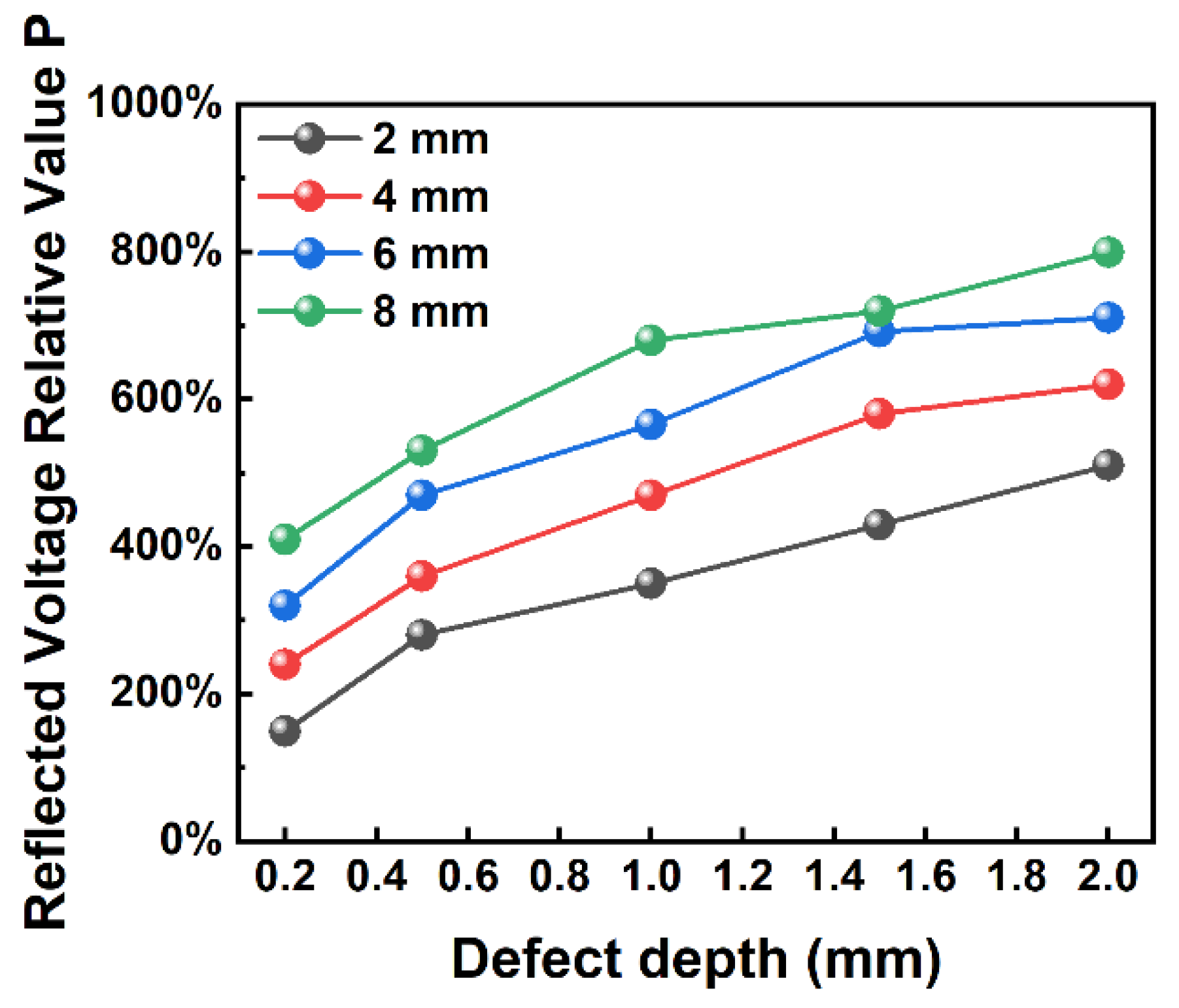
Rectangular grooves with depths of 0.2 mm, 0.5 mm, 1 mm, 1.5 mm, and 2 mm, and widths of 2 mm, 4 mm, 6 mm, and 8 mm, and a length of 10 mm, were pre-fabricated at the center of the surface of different flat XLPE samples to simulate air gap defects of varying sizes. The experimental results are shown in
Figure 14.
From the chart, it can be observed that as the defect depth increases, the relative reflection voltage increases, regardless of the defect width. Additionally, at the same defect depth, the larger the defect width, the higher the relative reflection voltage. This indicates that both the defect depth and width have an impact on the relative reflection voltage. The deeper the defect and the wider the defect, the larger the relative reflection voltage, meaning that as the defect size increases, the detection effect becomes more apparent. This further verifies the feasibility of using microwave detection for the detection of defects of varying sizes.
5.4.2. The Impact of Different Silicone Rubber Thicknesses on Detection Results
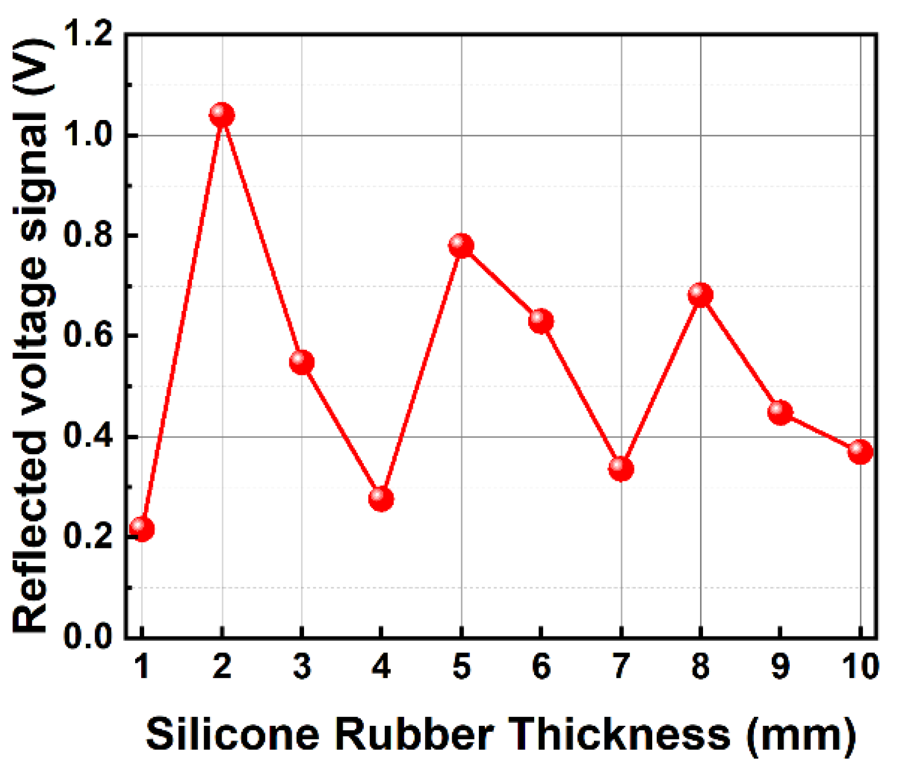
Flat samples were selected, using silicone rubber plates of varying thicknesses ranging from 1 to 10 mm. One sample was created for each 1 mm increment in thickness. During testing, the waveguide probe was placed in close contact with the surface of the sample. For each sample, the reflection signal intensity at five different positions was measured, and the average value was taken. The experimental results are shown in
Figure 15.
As shown in
Figure 15, the reflection signal exhibits a distinct fluctuating trend with increasing thickness, rather than a nonlinear monotonic change. When the thickness is 2 mm, the reflection signal reaches its maximum value. A significant drop occurs in the range of 3–4 mm. As the thickness further increases, secondary peaks appear near 5 mm and 7 mm, respectively. When the thickness is increased to 9–10 mm, the reflection signal levels off and remains at a relatively low level.
5.4.3. The Impact of Different Detection Distances on Detection Results
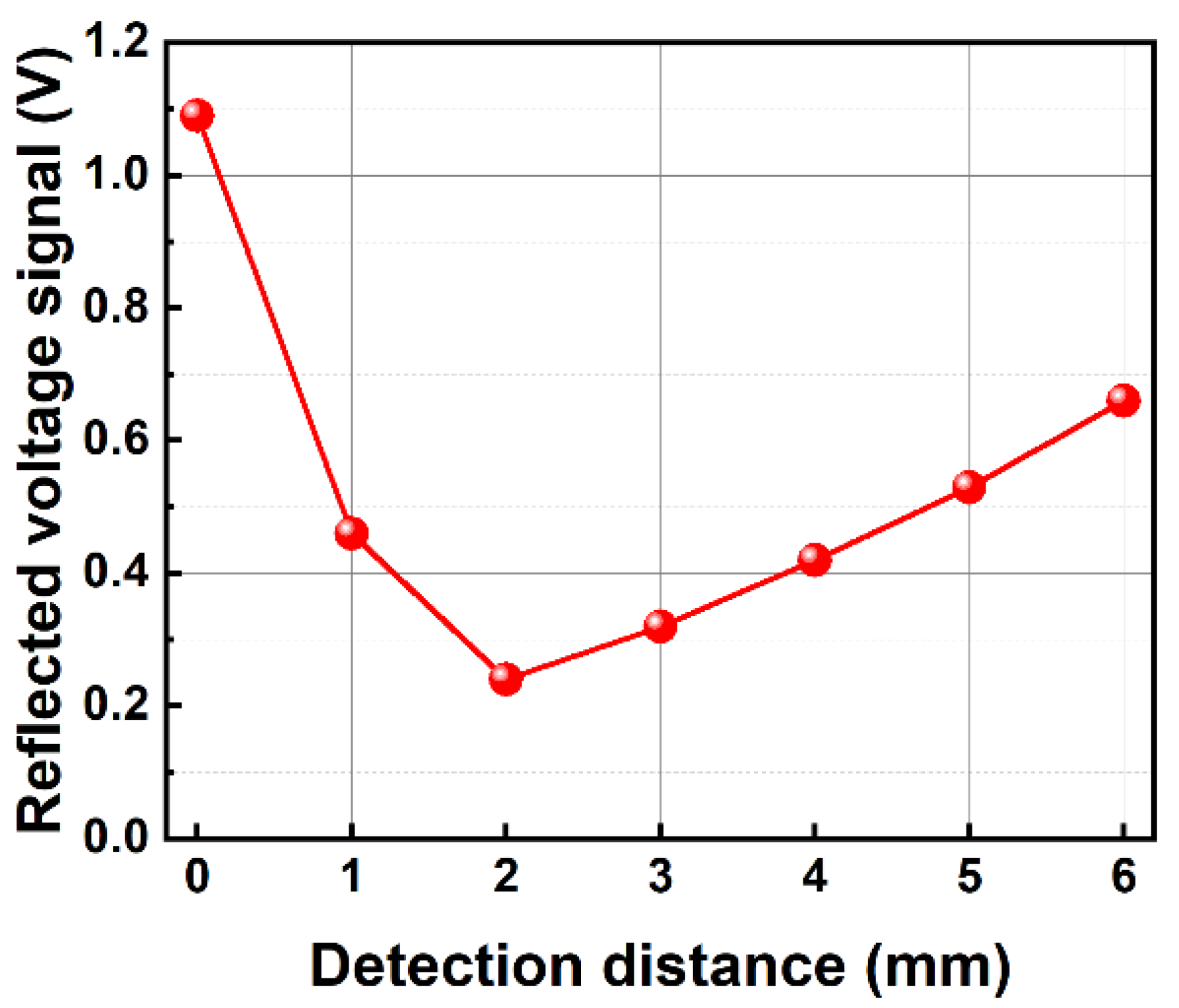
The flat sample with the optimal frequency from previous studies was selected to investigate the impact of detection distance h on the reflection voltage U. The detection distances h = 0 mm, 1 mm, 2 mm, 3 mm, 4 mm, 5 mm, 6 mm were tested. For each detection distance, experiments were conducted on the same defect-free flat sample. At each detection distance, reflection voltage U was randomly measured at 5 positions, and the average value was taken. The reflection voltage U at different detection distances h is shown in
Figure 16.
As shown in
Figure 16, the reflection voltage exhibits a nonlinear trend of “rapid initial decrease, followed by gradual recovery” with the change in detection distance. When the probe is in close contact with the sample surface (h = 0), the near-field strong coupling results in the maximum reflection signal. As the detection distance increases to 1–2 mm, the coupling field strength rapidly attenuates, causing the reflection voltage to drop to its lowest value. When the detection distance further increases to 3–6 mm, the reflection path gradually transitions from near-field coupling mode to free-space propagation mode, resulting in a slight increase in reflection voltage. This result indicates that the microwave reflection method is highly sensitive to the detection distance, maintaining high energy coupling efficiency and defect identification sensitivity only within a small gap range. This characteristic is of significant reference value for the practical detection of cable joints in subsequent applications.
5.4.4. The Impact of Different Detection Angles on Detection Results
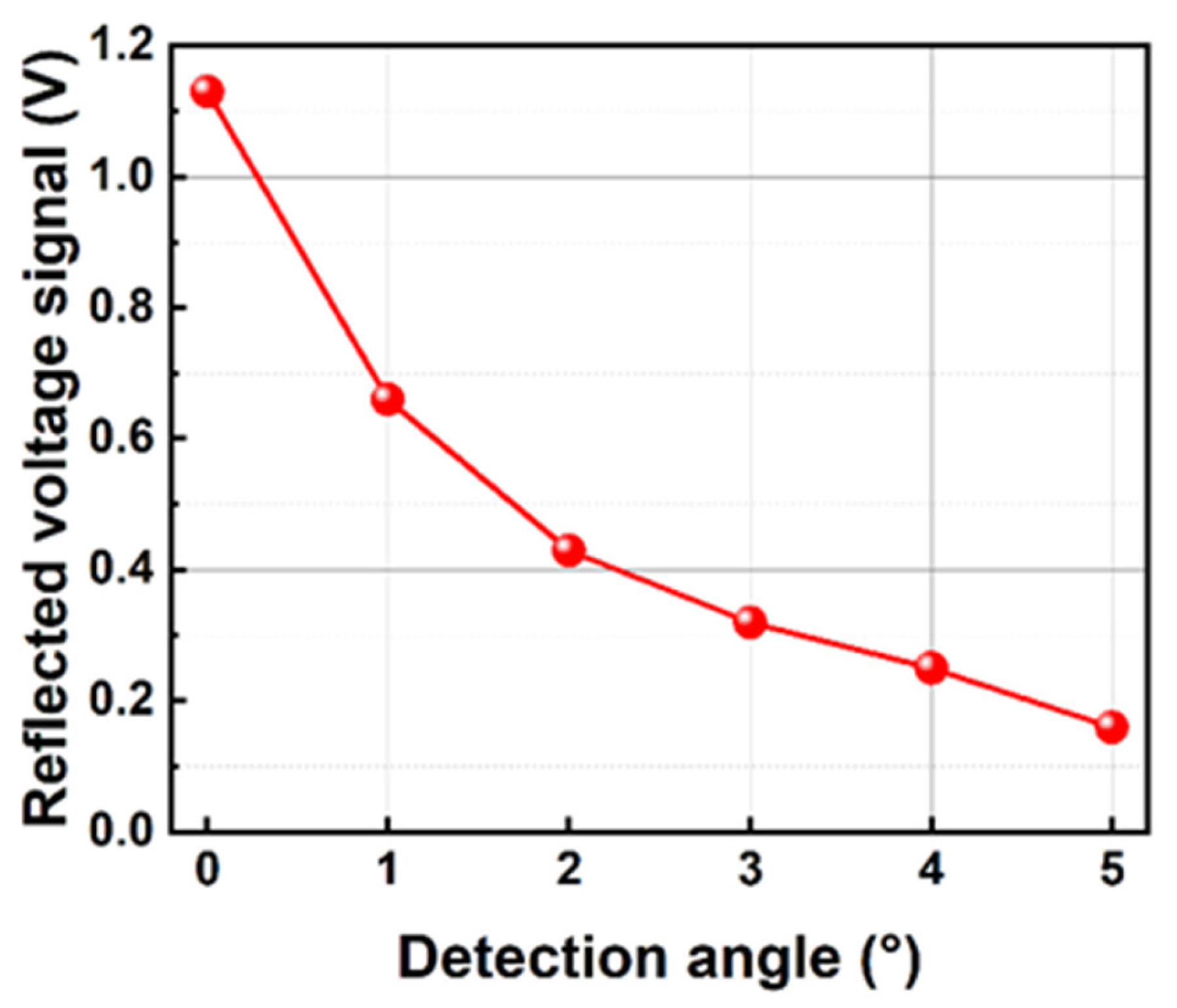
Since the detection relies on the intensity of reflected microwave signals, any variation in the sample’s angle during the detection process can cause changes in the received reflection signal, leading to interference in the detection judgment. Therefore, it is necessary to study the relationship between the angle formed by the plane of contact between the sample and the probe (referred to as the detection angle) and the strength of the microwave reflection signal. As the angle is introduced, flat and cylindrical samples can no longer be well-equivalent, so a cold-shrinkable intermediate joint sample is used for the experiment.
As shown in
Figure 17, the reflection voltage exhibits a distinct monotonic decrease with the increase in detection angle. When the detection angle is 0°, the probe is completely in contact with the joint surface, and the incident microwave aligns with the normal direction of the interface, resulting in the strongest near-field coupling and the highest reflection signal amplitude. As the detection angle gradually increases, the effective projection of the contact area decreases, the incident direction deviates from the normal, and the returning energy significantly attenuates, causing the reflection voltage to continuously decrease. At 5°, the reflection signal becomes very small compared to the initial value, indicating that even a slight angular deviation can have a significant impact on detection sensitivity. This result demonstrates that the detection angle is an important factor influencing the coupling efficiency between the waveguide aperture and the tested structure. When there is inclined incidence, part of the energy may propagate along the sheath surface or dissipate in the form of radiation, making it difficult to effectively couple back into the waveguide port, leading to a decrease in the apparent reflection coefficient. Therefore, in practical cable joint inspections, it is crucial to ensure that the probe maintains as close to normal incidence as possible with the joint’s outer surface; otherwise, it will affect the distinguishability of defect reflection characteristics and the stability of the detection results.