1. Introduction
DC–DC converters, such as the buck, boost, flyback, and forward converters, are widely used in low- to medium-power applications due to their simple topology and low cost [
1,
2]. However, the system power continues to rise, and even in high-power applications, voltage spikes may occur during switching due to the freewheeling problem caused by the inductors of the power converter. The higher the system power, the greater the voltage spike. Thus, a half-bridge isolated LLC converter appears to adapt to higher-output-power applications [
3].
The traditional half-bridge LLC converter is operated by two power switches on the primary side, and a sinusoidal wave current is generated in the resonant circuit by complementary switching. The voltage gain is determined by the converter and the transformer. Thus, a stable output voltage is obtained by adjusting the switching frequency according to the input voltage.
The resonant current is a sinusoidal wave provided that the switches can be turned on at zero voltage. If the frequency is adjusted properly, the rectifier on the secondary side can be turned off at zero current. Therefore, the switching loss is significantly reduced and the efficiency is improved.
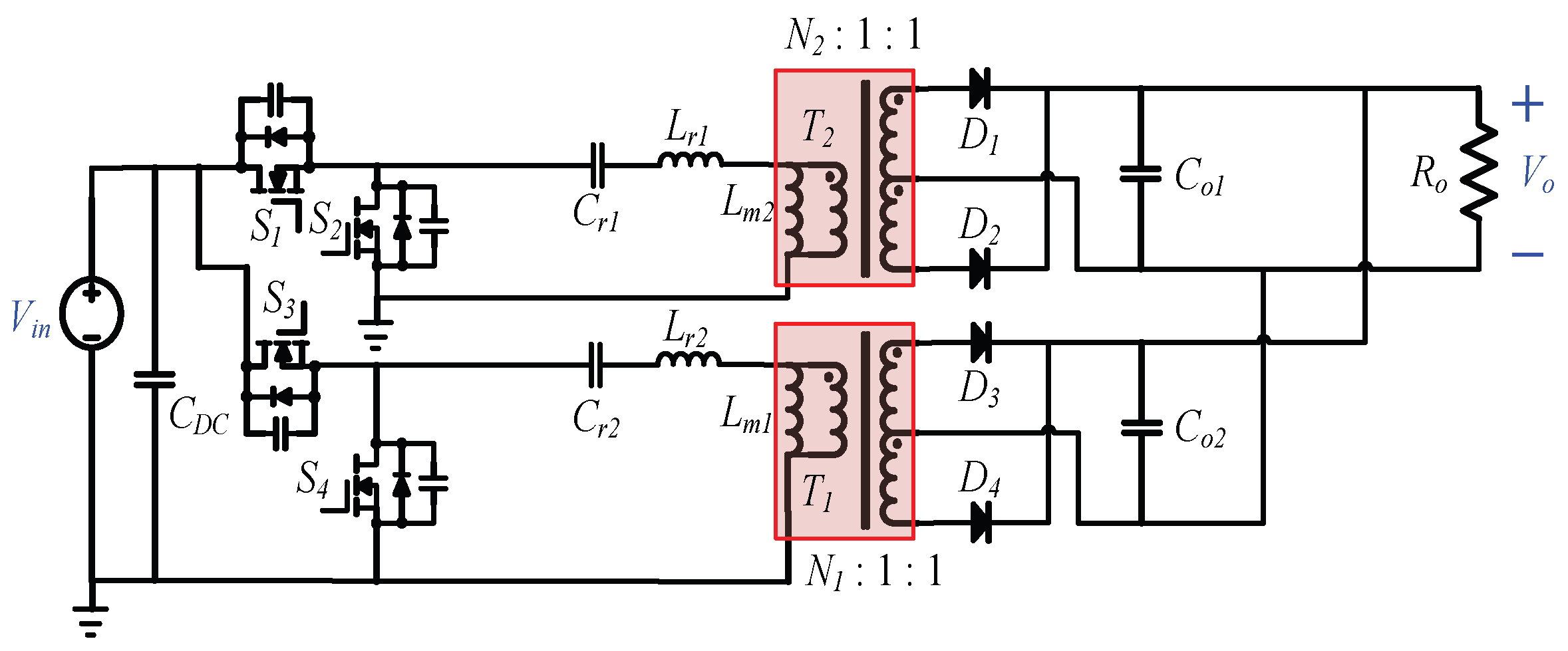
In [
4], a converter with two parallel half-bridge resonant circuits was proposed, as shown in
Figure 1. The proposed converter can improve the output power of the converter and reduce the power stress of the components. Several different parallel topologies have been reported. The use of fly capacitors to equalize the resonant current of a parallel two-phase circuit was proposed in [
5]. However, the equalization performance was poor. In [
6,
7,
8,
9,
10,
11], two half bridges were connected in parallel on the primary side and the outputs in series on the secondary side. In [
12], a TL DC–DC converter using phase-shift control was studied. Nevertheless, the circulating current problem cannot be ignored.
In [
13], a converter with a six-switch dual active bridge and a series transformer, which connected series on the primary side and the secondary side, was proposed. However, it can only reduce the voltage stress of upper and lower switches.
In the converters of [
14,
15], the magnetizing inductance of the transformer can be changed to reduce the conduction loss. In [
16,
17,
18,
19,
20,
21,
22], the hybrid bridge structure of the primary side or topology morphing method was applied on an LLC converter. However, the current stress on the secondary side could not be effectively reduced.
In [
23], the converter combined an interleaved boost circuit and a full-bridge resonant circuit on the primary side to narrow the voltage gain range and reduce the voltage stress of the switch. However, this made the circuit complicated, and the power stress on the secondary side could not be further reduced. In [
24], a traditional half-bridge LLC converter was used and PFM and APWM methods were adopted for the switching operation. Although this was able to narrow the switching frequency range, the zero-voltage switching (ZVS) condition sometimes disappeared.
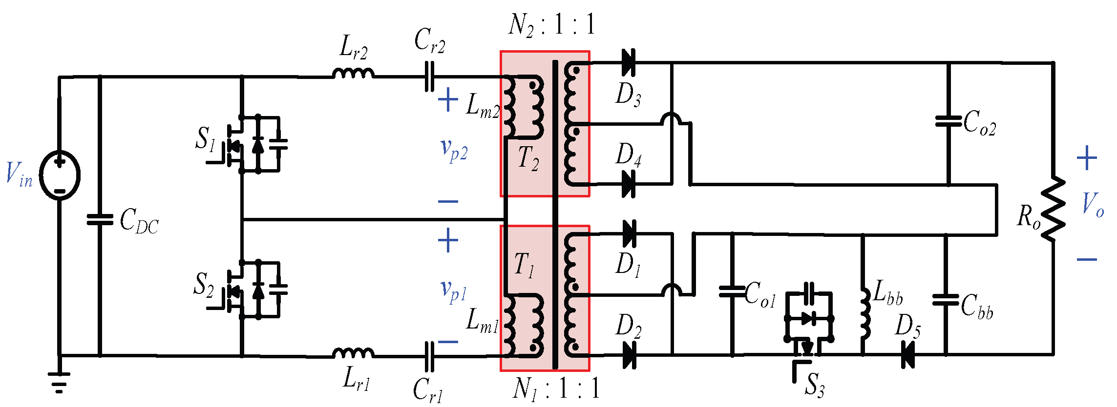
This paper proposes an LLC converter with parallel dual half-bridge resonant circuits. The dual circuits are used to distribute power to reduce the power stress of components and improve the power capacity of the proposed converter. The proposed converter is consisted of an LLC part and buck–boost part. The LLC part operates in a DCX state and the switching frequency is fixed at a resonant frequency. Moreover, the primary side switches and the secondary side diodes of the LLC part can satisfy the conditions of ZVS and zero-current switching (ZCS), respectively. The buck–boost part can achieve a wide output voltage range with pulse-width modulation (PWM).
Compared with the traditional parallel dual half-bridge resonant converter, the proposed converter shown in
Figure 2 saves two active switches. Thus, the additional conduction loss and switching loss caused by the two switches are reduced. The design of magnetic components becomes simple due to fixed-frequency operation. An experimental prototype with input voltage of 384 V, output voltage of 24–40 V, and power of 80 W was established and tested. The experimental results are provided to verify the system’s performance.
2. Principle of Operation
A parallel dual half-bridge resonant LLC converter with a wide range of output voltages, as shown in
Figure 2, is proposed in this paper. The primary side of the proposed converter consists of two parallel half-bridge structures with shared switches
S1 and
S2. The LLC resonant tanks are constructed by the resonant elements
Lr1,
Lr2,
Cr1, and
Cr2 and the magnetizing inductances of transformers
Lm1 and
Lm2. Center-tapped transformers are used as
T1 and
T2.
S3,
Lbb, and
D5 are combined to form the buck–boost part. The buck–boost part is operated in continuous conduction mode (CCM) and regulates the output voltage of the proposed converter with pulse-width modulation (PWM). The switching frequency of
S3 is not equal to the switching frequencies of
S1 and
S2.
In order to simplify the analysis of the proposed converter, the following assumptions will be considered to describe the converter operation and steady-state analysis.
The duty cycle of switches S1 and S2 in the primary side is fixed at 0.45.
All switches have parasitic capacitances and bypass diodes, and transformers have certain magnetizing inductance, regardless of leakage inductance.
The primary side switches S1 and S2 have a dead time.
Each output capacitor in the secondary side is large enough to keep the output voltage constant.
All capacitors, inductors, and diodes are ideal components.
Based on the above assumptions, there are six modes during one period of the operation of the proposed converter. The operation modes and key waveforms of the converter are shown in
Figure 3 and
Figure 4, respectively.
2.1. Operation Principle
There are six modes in one period of the converter operation.
Mode 1 [
t0–
t1]: As shown in
Figure 3a, at
t =
t0,
S2 is turned off,
D1 and
D4 turn into conduction mode, and the converter enters dead time. At this time, the resonant current
iLr1 is negative and
iLr2 is positive, and thus the parasitic capacitance of
S2 (
Coss2) begins to charge until it reaches
Vin and then
S2 turns off, and the parasitic capacitance of
S1 (
Coss1) begins to discharge.
S3 remains turned off and
Lbb continually releases energy to load through
D5. Since the magnetizing inductance does not participate in the resonance, the magnetizing current of
Lm1 and
Lm2 rises and falls linearly, respectively. This mode ends when
Vcoss2 is charged to
Vin and
Vcoss1 is discharged to 0 V.
Mode 2 [
t1–
t2]: As shown in
Figure 3b, at
t =
t1,
S1 is turned on with ZVS.
iLm1 and
iLm2 are increasing and decreasing, respectively, in this mode.
S2 is completely turned off. At this time, due to the freewheeling of the resonant currents
iLr1 and
iLr2, they flow through
S1. The resonant current
iLr1 rises, and
iLr2 falls as the sinusoidal waveform. The energy is delivered to the load through
D1 and
D5.
Mode 3 [
t2–t3]: As shown in
Figure 3c, at
t =
t2,
S3 turns on,
Lbb stores energy through
D1, and the current of
D5 is decreased to zero. At this time, the resonant current
iLr1 begins to turn into a positive current, and
iLr2 begins to turn into a negative current. This mode ends when
iLr1 is equal to
iLm1 and
iLm2 is equal to
iLr2.
Mode 4 [
t3–
t4]: As shown in
Figure 3d, at
t =
t3,
D1 and
D4 are turned off with ZCS. Since the magnetizing inductances
Lm1 and
Lm2 represent part of the resonance with
Lr1,
Cr1,
Lr2, and
Cr2,
iLr1 is the same as
iLm1 and the difference between
iLm2 and
iLr2 is zero.
Vin cannot deliver energy to load through
D1 or
D4 during this mode.
iLbb increases continually due to
Co1 supplying energy to
Lbb, while
Co2 and
Cbb provide energy to the load. When
S1 is turned off, this mode ends and enters the negative cycle of operation of the proposed converter.
Mode 5 [
t4–
t5]: As shown in
Figure 3e, at
t =
t4,
S1 is turned off,
D2 and
D3 are conducted, and the converter enters dead time.
Vin is delivering energy to load and
Lbb through
D2 and
D3. At this time, the resonant current
iLr1 is positive and
iLr2 is negative, and thus the parasitic capacitor of
S1 starts to charge until it reaches
Vin and the parasitic capacitor of
S2 begins to discharge. This mode ends when
Vcoss2 is discharged to 0 V and
Vcoss1 is charged to
Vin.
Mode 6 [
t5–
t6]: As shown in
Figure 3f, at
t =
t5,
S2 turns on with ZVS. At this time, the resonant current
iLr1 begins to turn into a negative current and
iLr2 begins to turn into a positive current. The input energy is sent to the load through
D3. After the end of mode 6,
iLr1 is equal to
iLm1 and
iLm2 is equal to
iLr2.
2.2. Parameter Calculation
The input voltage of the proposed converter is 384 V, the output voltage is from 24 V to 40 V, the maximum output power is 80 W, and the switching frequency is 107 kHz. Since the output voltage is determined by the buck–boost circuit on the secondary side, the output of the LLC resonant tank is 12 V.
The voltage gain of the LLC resonant circuit is obtained from the equivalent impedance of the circuit, and the formula is expressed as follows.
If the gain
G is 1, the turn ratio is 16 from (1), and
Fx is the frequency ratio. In order to keep the gain
G at 1, the resonance frequency selected is 107 kHz, which is the same as the switching frequency.
The resonant frequency can be obtained from Equation (3). Since 107 kHz is selected as the resonant frequency, the resonant inductor and resonant capacitor can be obtained. Thus, the resonant inductance is 81.04μH and the resonant capacitance is 27.3 nF.
In addition, m is the inductance ratio, which is designed to be 11 and makes the ratio of Lm/Lr = 10. The larger the inductance ratio, the smaller the resonant inductance value can be, thereby reducing the volume and loss of the resonant inductance.
The ratio cannot be too large: otherwise, the leakage inductance of the transformer may be greater than the resonant inductance, resulting in a different circuit from the original design.
Q is the quality factor for the circuit. In order to keep a stable current gain on the secondary side, the quality factor selected is 0.134. This may make the voltage gain curve slightly steep and the range of variation wider than usual. Fortunately, the range of variation in input voltage is between −10 V and 10 V, which is acceptable.
The equivalent impedance
Req in (5) is expressed as follows.
Figure 5 shows the gain curves of different quality factors (
Q). It can be seen that the gain curve with
Q = 0.134 is the steepest. This can be reserved for future adjustment if the voltage regulation circuit is removed, which would mean the range would be adjustable by frequency modulation only.
4. Experimental Results
To verify the simulation results of the proposed converter, an experimental prototype of a dual half-bridge LLC resonant converter was constructed and tested with different output voltages, as shown in
Figure 14. The circuit specifications are:
Vin = 384 V,
Vo = 24–40 V, and
Po = 80 W. A TSM320F28335 DSP controller from Texas Instruments was used for the system control.
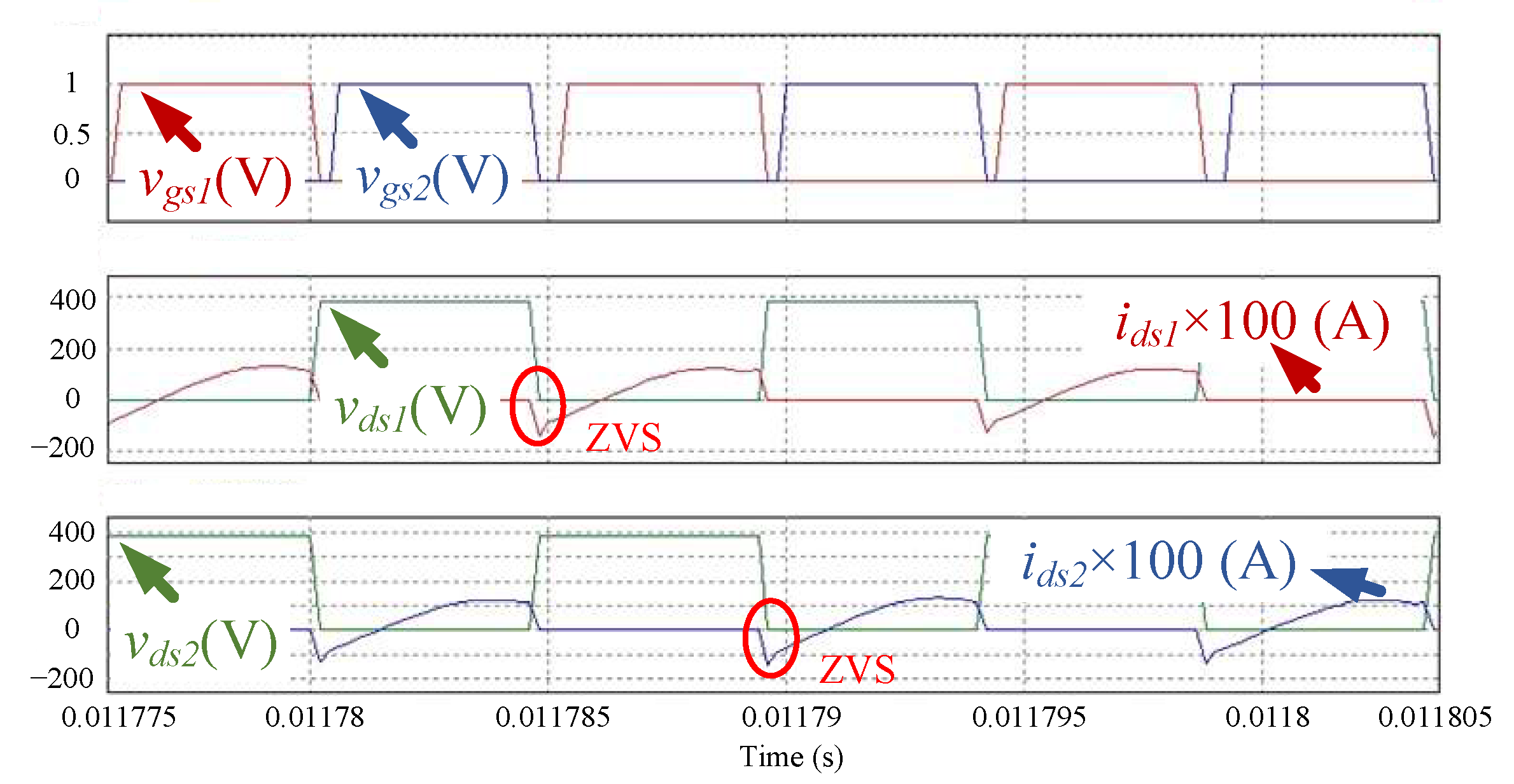
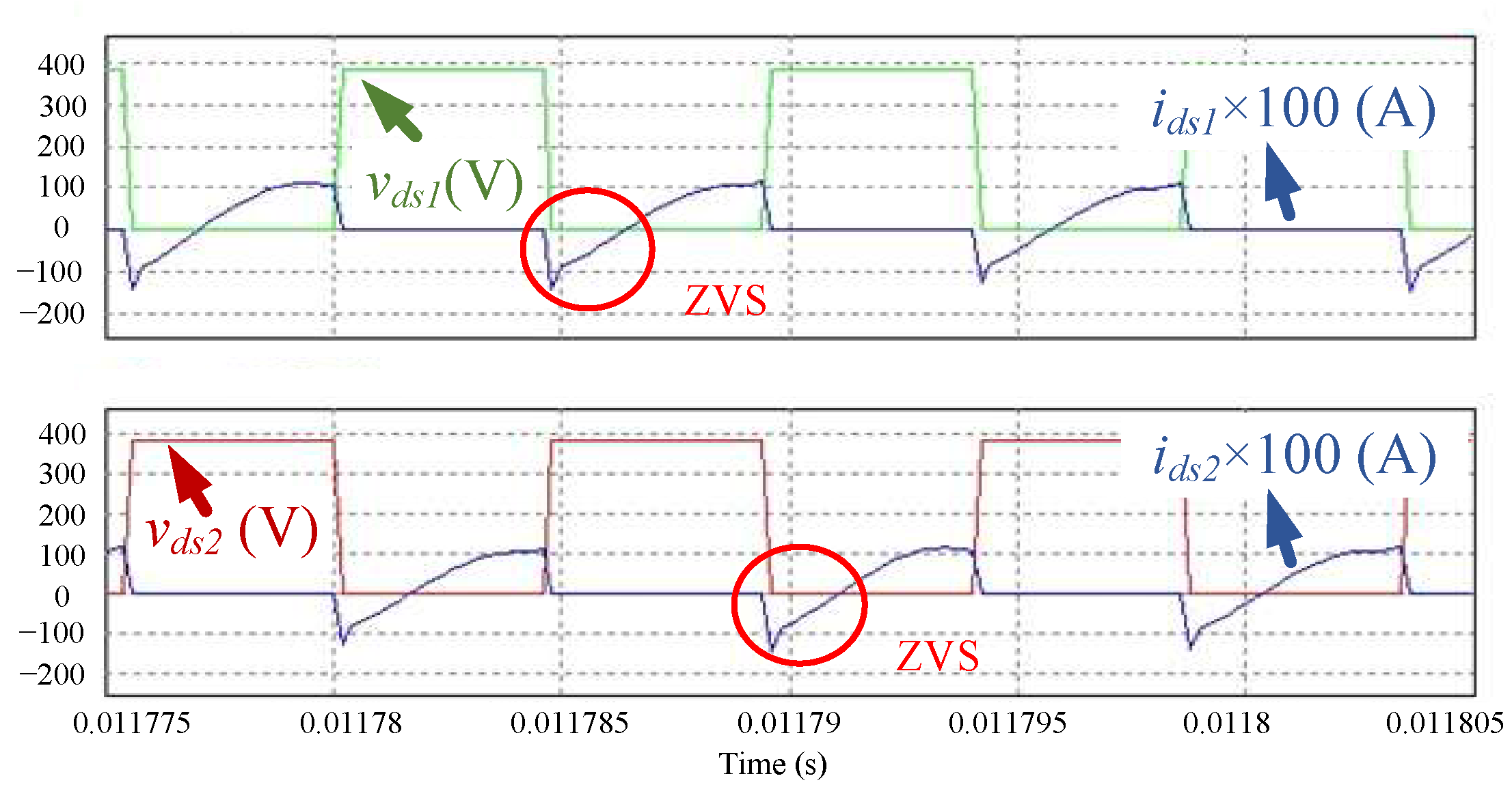
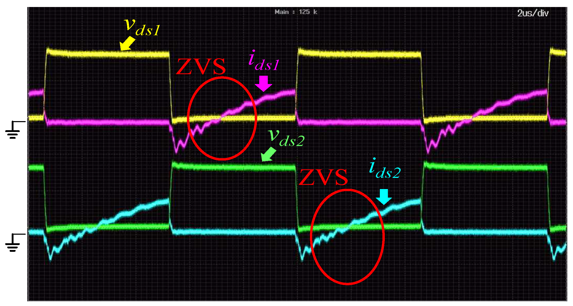
Figure 15 shows the measured waveforms of the primary side switches
S1 and
S2 when the input voltage is 384 V and the output is 10% of rated load.
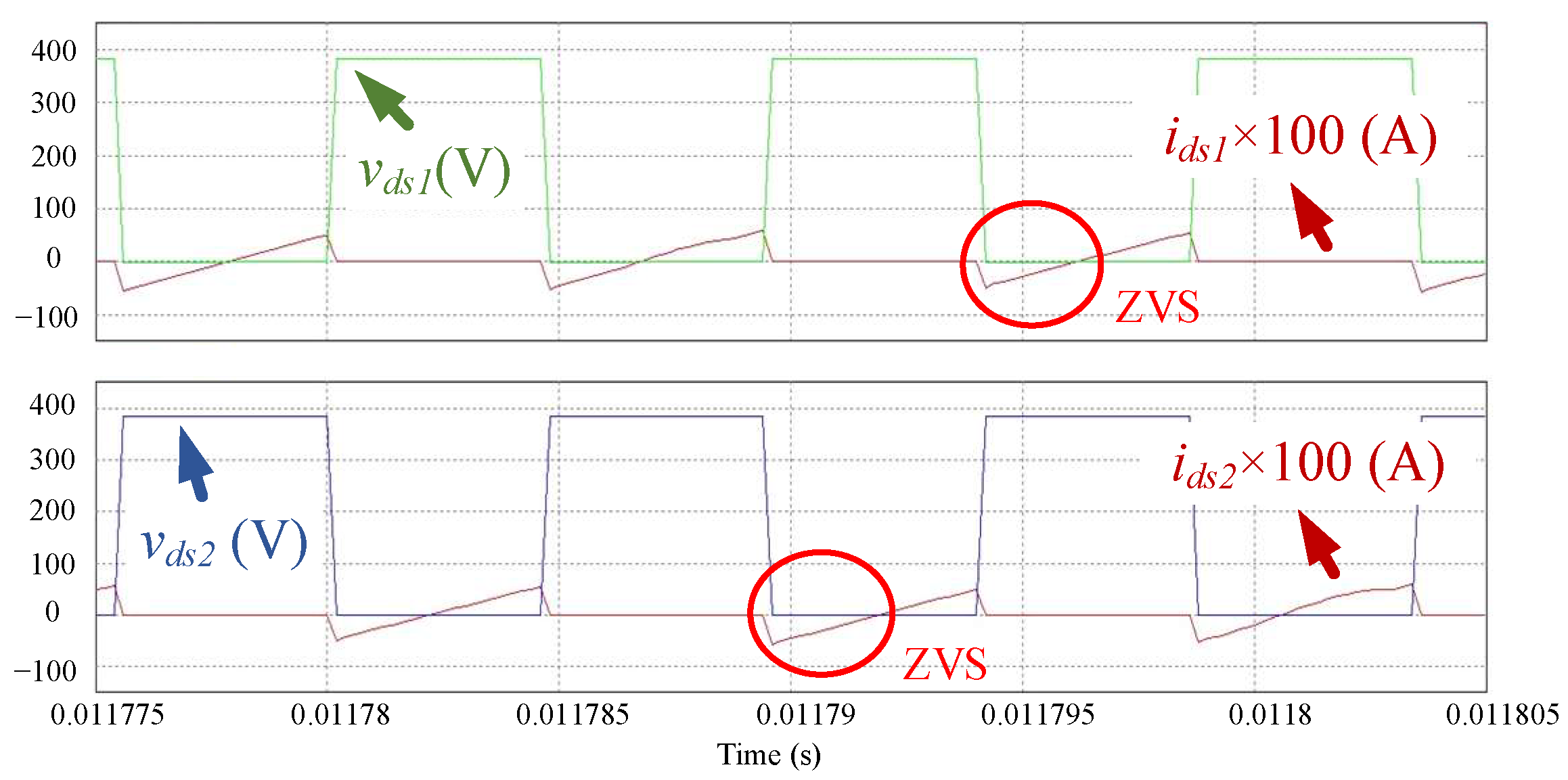
Figure 16 shows the measured waveforms of the primary side switches
S1 and
S2 when the input voltage is 384 V and the output is 50% rated load.
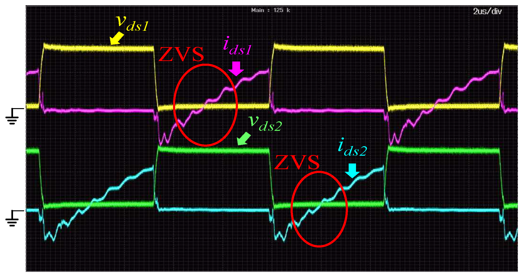
Figure 17 shows the measured waveforms of the primary side switches
S1 and
S2 when the input voltage is 384 V and the output is 100% rated load. It can be found from the measured waveforms that ZVS turn-on of the proposed converter is achieved for the light-load, half-load, and full-load conditions.
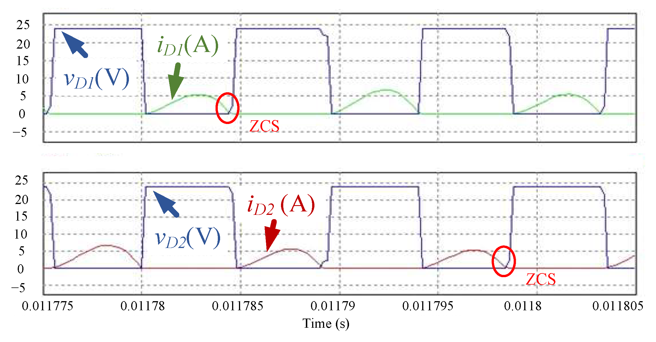
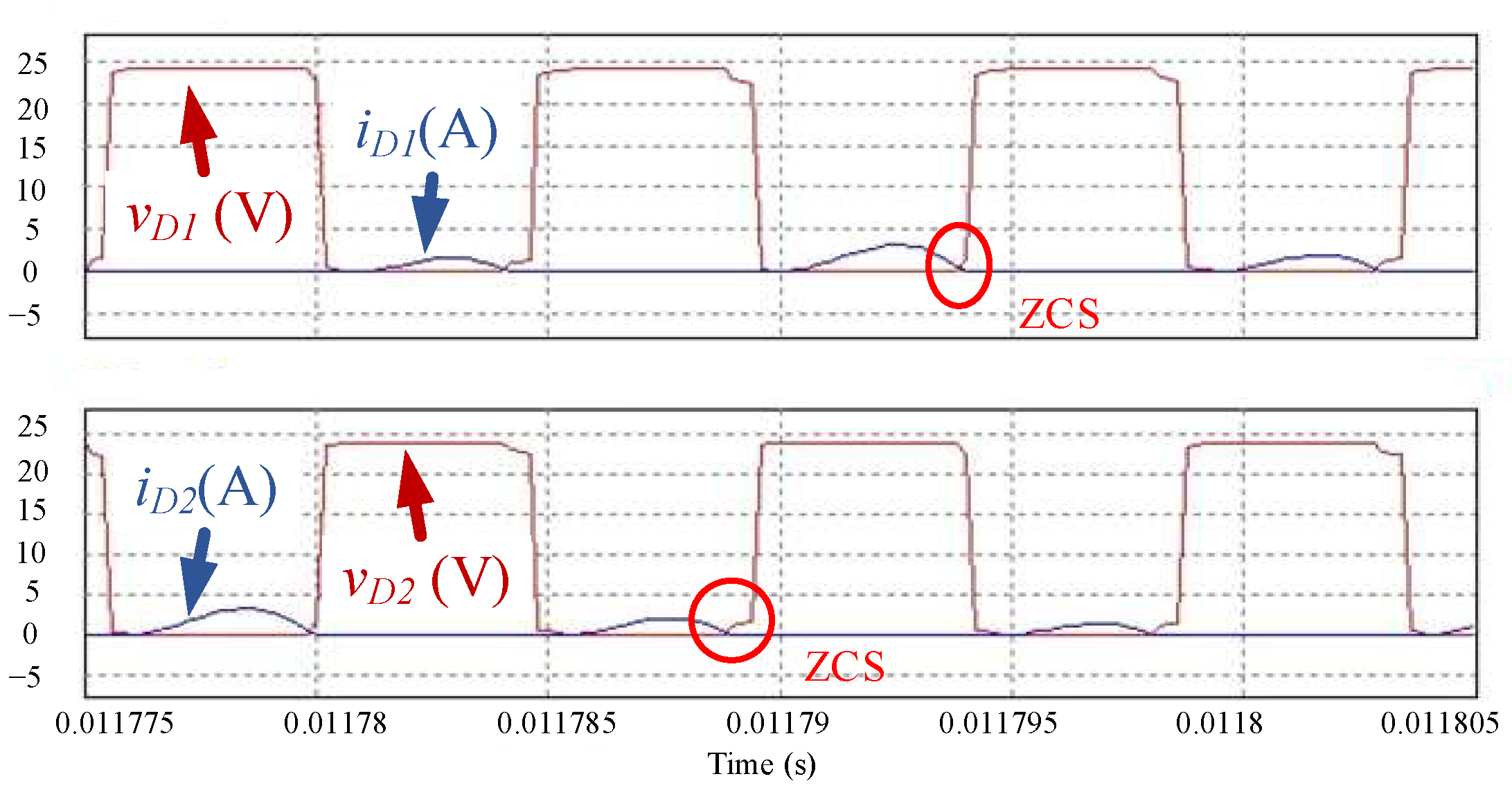
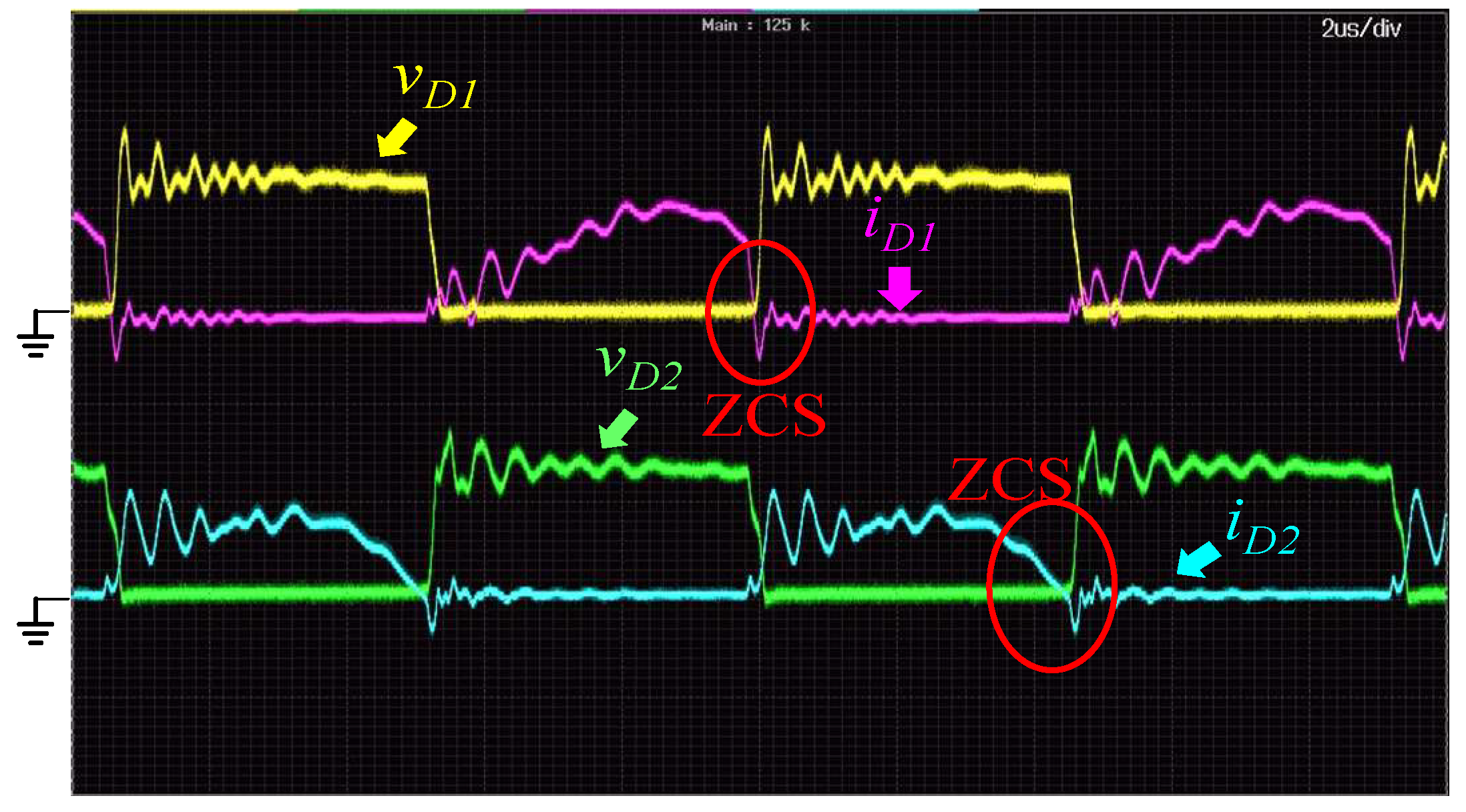
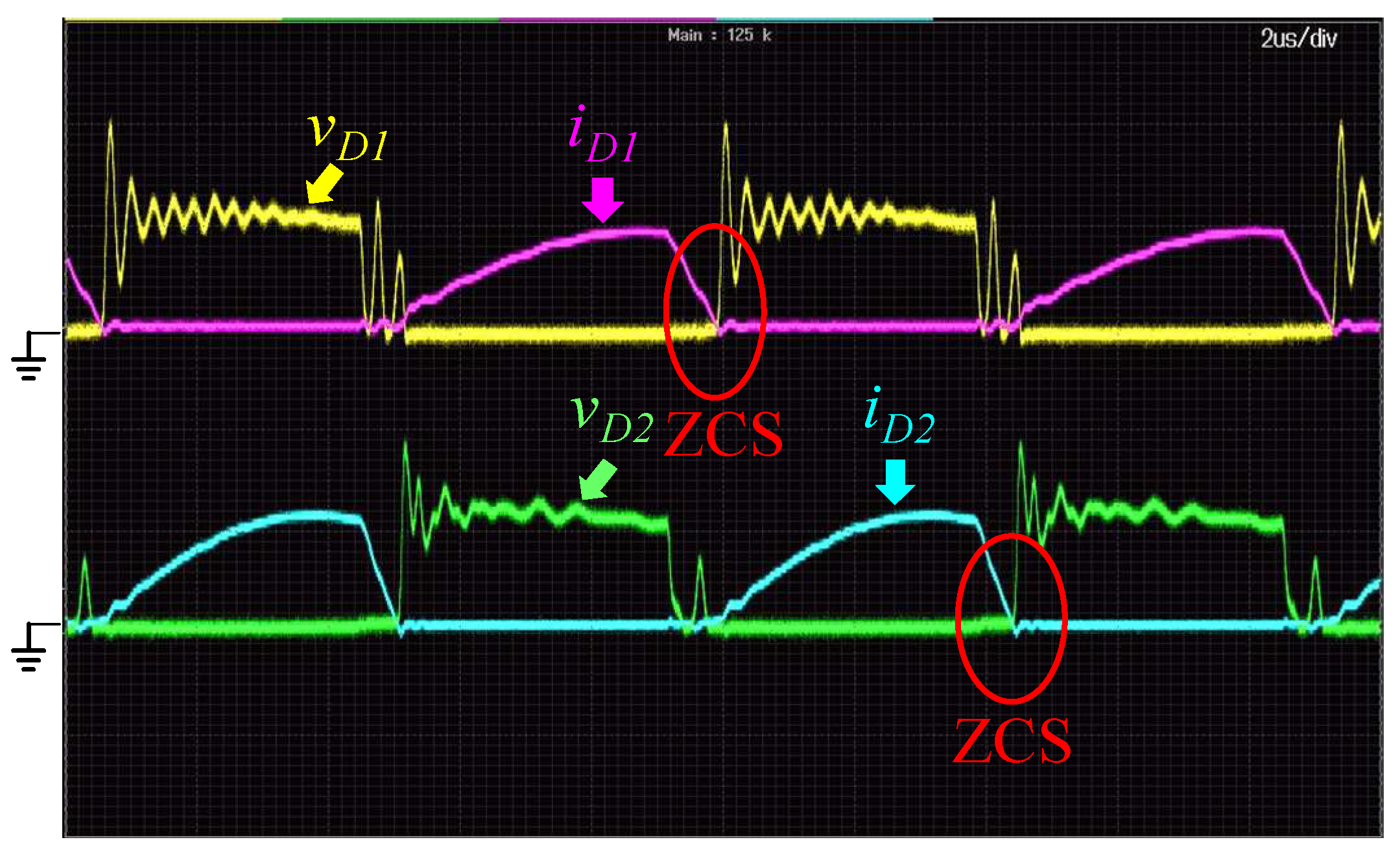
Figure 18 shows the measured waveforms of the rectifier diodes
D1 and
D2 on the secondary side, and the output is 10% rated load.
Figure 19 shows the measured waveforms of the rectifier diodes
D1 and
D2 on the secondary side, and the output is 50% rated load.
Figure 20 shows the measured waveforms of the rectifier diodes
D1 and
D2 on the secondary side, and the output is 100% rated load. Zero-current switching (ZCS) is achieved under light-load, half-load, and full-load conditions. The excellent performance of the proposed converter is verified by the experimental results. It is obvious from
Figure 21 and
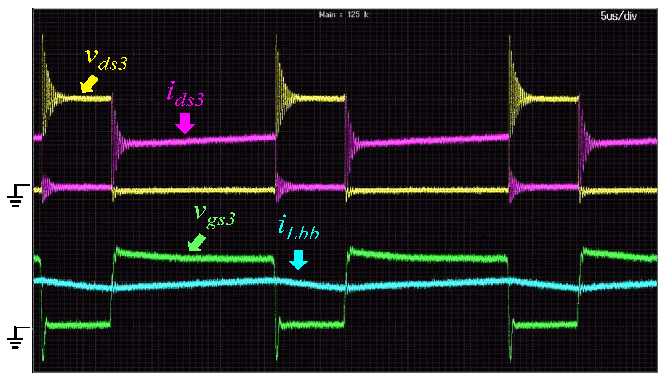
Figure 22 that the storage inductors are both operating in continuous conduction mode (CCM). In
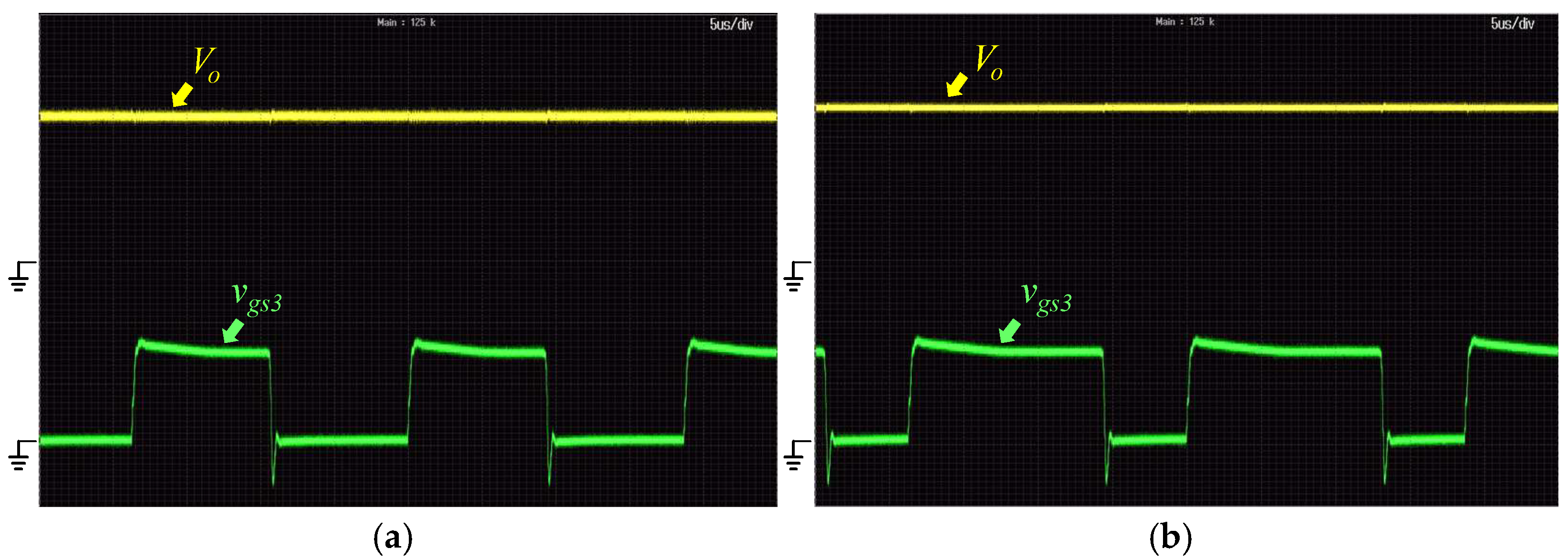
Figure 23a, if the duty ratio of switch
S3 is 0.5, the output voltage is 24 V.
Figure 23b shows that the output voltage is 40 V when the duty ratio is 0.7.
Since the proposed converter can achieve ZVS turn-on at
S1 and
S2 and ZCS turn-off at
D1–
D4, power loss analysis for the converter can be divided into several main components, namely the conduction loss, switching loss of
S3, turn-off loss of
S1 and
S2, reverse recovery loss of
D5, and transformer loss. The conduction loss of the switching device
PS_cond and diode
PD_cond can be expressed as the following:
where
rD and
RDS(ON) are the internal resistance of the diode and switch, respectively,
Irms is the effective value of the switch or diode current,
Iavg is the average current of the diode, and
VF is the forward voltage drop of the diode.
Practically, the capacitors have equivalent series resistance (ESR) and the inductors have direct current resistance (DCR). Therefore, the conduction loss of capacitors
PC_cond and inductors
PL_cond must be considered in total power loss of the proposed converter.
PC_cond and
PL_cond can be calculated as (9) and (10), respectively:
where
IC_rms and
IL_rms are the rms current of capacitors and inductors, respectively,
ESR is the equivalent series resistance of capacitors, and
DCR is direct current resistance of inductors.
The switching loss of the power switch
Psw can be expressed as the following formula:
where
VDS is the DS terminal voltage of the switch,
IDS is the current of the switch,
fs is the switching frequency, and
toverlap is the overlapping time between
vDS and
iDS of the switch, as shown in
Figure 24. The turn-off loss of
S1 and
S2 can also be calculated by (11).
Because of the characteristics of soft switching only being achieved at
D1–D4,
D5 will generate reverse recovery loss
Prr when it is turned off. The formula of
Prr can be obtained as:
where
Vr is the reverse voltage of the diode,
Irr is the reverse recovery current of the diode, and
trr is the reverse recovery time of the diode.
Transformer loss includes winding loss
PT_w and core loss
PT_core. Since the calculation of winding loss is similar to (10),
PT_w will not be mentioned here. Core loss can be estimated using the Steinmetz equation:
where
K, α, and β are coefficients from the datasheet of core material and ∆
B is the magnetic flux variation of transformer.
The overall converter efficiency
η can be obtained by the following formula:
where
Po is the output power and
Ploss is the total power loss.
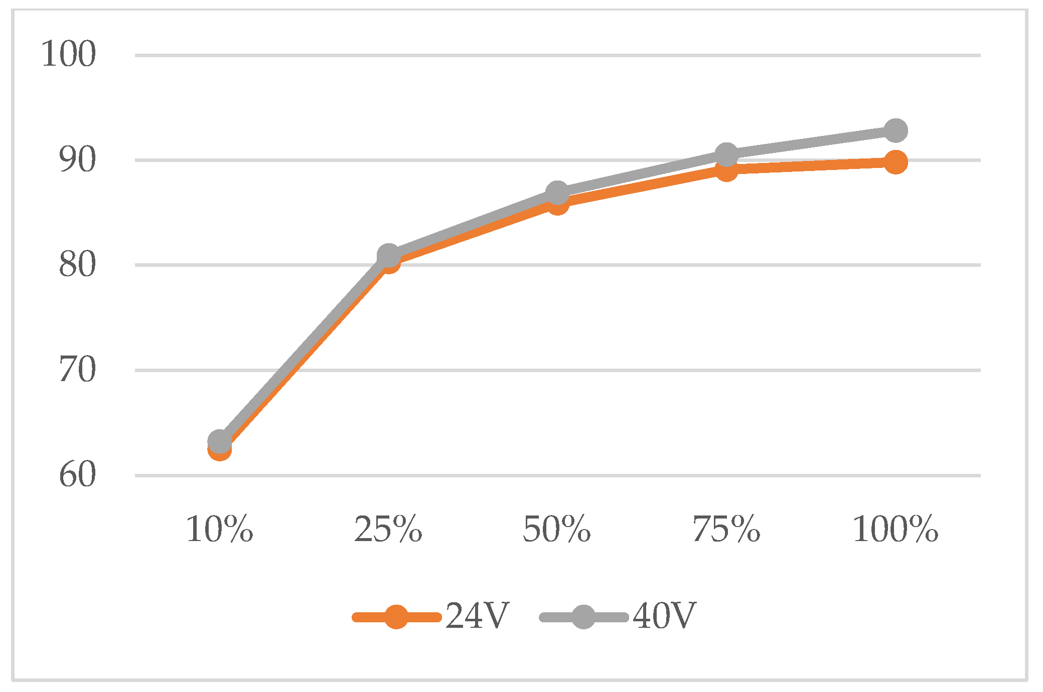
Figure 25 shows the efficiency curves of the converter at different output voltages. It can be observed in the curves that the highest efficiency reaches 92.8% at 80 W. The efficiency of the converter decreases directly proportional to the load.
Figure 26 shows the sum of different power losses of the proposed converter when the output voltage is 40 V at full load, including the switching loss of switches, the conduction loss of switches, the reverse recovery loss of diodes, the conduction loss of diodes, the conduction loss of resonant and magnetic components, the core loss, and the winding loss. As
Figure 26 shows, the total power loss of the proposed converter is obtained at 6.21 W, and the LLC part is around 66.49% of the entire power loss. In the power loss of the LLC part, the core loss is the majority loss and the conduction loss of
S1 and
S2 is the minority loss. Most of the loss in the buck–boost part is due to the conduction loss of
L3. On the contrary, the reverse recovery loss of
D5 is the lowest.
Table 2 gives a performance comparison for the proposed converter with three different converters. As
Table 2 shows, the proposed converter and other converters in [
5,
6,
14] used two transformers and achieved the ability of soft switching. The proposed converter uses the fewest switches compared with [
5,
6,
14]. Moreover, ref. [
14] is the only converter that used the relay in
Table 2. The converter using pulse-frequency modulation (PFM) regulates voltage by varying the switching frequency and requires a wide switching frequency range [
5,
14,
25]. However, the wide switching frequency range increases the difficulty of the design of the magnetic component. Pulse-width modulation (PWM) and phase-shift modulation (PSM) are the fixed-frequency modulations that simplify the magnetic component design. The voltage range of the proposed converter is wider than the other converters in
Table 2 even when the proposed converter is not the best in terms of efficiency. Therefore, the proposed converter is a good choice in medium- or low-power applications.


