Article

A Single-Phase Compact Size Asymmetrical Inverter Topology for Renewable Energy Application

1
Department of Electrical Engineering, Z. H. College of Engineering & Technology, Aligarh Muslim University, Aligarh 202001, India
2
Center for Energy Transition, Universidad San Sebastián, Santiago 8420524, Chile
3
High-Power Converter Systems (HLU), Technical University of Munich (TUM), 80333 Munich, Germany
4
Electrical Engineering Department, Faculty of Engineering, Assiut University, Assiut 71516, Egypt
*
Authors to whom correspondence should be addressed.
Energies 2025, 18(19), 5121; https://doi.org/10.3390/en18195121
Submission received: 23 August 2025 / Revised: 16 September 2025 / Accepted: 22 September 2025 / Published: 26 September 2025
(This article belongs to the Section F3: Power Electronics)

Abstract

This paper presents an improved structure of an asymmetrical single-phase multilevel inverter topology with reduced device count. The proposed topology achieves 19 voltage levels at the output using only 12 power switches and 3 DC sources. The topology can be easily extended, resulting in a modular topology with more voltage levels at higher voltages. Moreover, the reliability analysis of the proposed converter results in a higher mean time to fault. The simulation is performed in MATLAB/Simulink, and a hardware prototype is developed to validate the circuit’s performance. A low-frequency Nearest Level Control PWM technique is implemented to generate switching signals and achieves 4.30% THD in output voltage. The PLECS software is used for power loss and efficiency analysis, resulting in a maximum efficiency of 99.08%. The proposed converter has been compared with other MLI topologies to demonstrate its superiority. The results indicate that the proposed topology has proven superior and outperformed other topologies in various parameters, making it suitable for renewable energy applications.

1. Introduction

Multilevel inverters (MLIs) are advanced versions of two-level inverters suitable for medium and high-power applications. They consist of a network of power semiconductors and capacitive voltage sources, which, when interconnected and regulated, can produce a stepped voltage waveform closer to sinusoidal [1,2]. The increasing interest in renewable energy sources, such as solar photovoltaic and wind energy, has prompted the development of innovative technologies that can integrate with these systems. MLIs offer higher power quality waveforms, reduced harmonic content, lower electromagnetic compatibility concerns, and a modular structure, making them attractive for various applications [3]. Their modular structure leads to a more economical life cycle, easier maintenance, easier scaling, and better fault tolerance. MLIs also find applications in various fields, including industrial drives, Flexible AC Transmission Systems, High-Voltage Direct Current transmission, marine propulsion, electric vehicles, and active filters [4,5].
The conventional topologies of the multilevel inverters, including Diode Clamped or Neutral Point Clamped, Flying Capacitor, and Cascaded H-bridge multilevel converter, have the disadvantage of having a large number of device counts as the output voltage increases. The exponential increase in device counts leads to a significant increase in the complexity and size of the MLI, potentially resulting in higher costs, increased losses, and more challenging control and thermal management [6]. However, having more levels allows for a smoother output voltage waveform, potentially reducing the size of the output filter [7]. The large number of device counts has drawn the focus of researchers to propose a topology having fewer DC sources, gate drivers, and switch requirements under the name of reduced switch count (RSC) MLIs [8]. The authors of [9] provide a thorough analysis and classification of RSC-MLI topologies, examining their structure, features, limitations, and suitability for specific applications. RSC-MLIs can be categorized as Generalized RSC-MLIs, stacked topologies, Unit-based MLIs, switched-capacitor (SC) RSC-MLIs, Transformer-based RSC-MLIs, and three three-phase topologies. Generalized RSC-MLIs include topologies having separate levels and polarity generators; there is a backend H-bridge converter, which limits their applications in high-voltage applications. Some of the topologies without a backend H-bridge converter are Envelope (E-type) type, Square T-type (ST-type), K-type, Packed U Cell (PUC) type, and Switched DC-sources (SDS). The E-type, ST-type, and K-type topologies are unit-based topologies that cannot be extended directly to generate higher levels but can be extended by cascading suitable modules. ST-type was derived from E-type, and there is a reduction in switch count in ST-type compared to E-type, while K-type topology utilizes capacitors to reduce the DC sources. The ST-type topology in [10] employs 4 DC sources, 2 of which are of the same variety, and 12 power switches to produce 17 levels at the output. The topology in [11] is a K-type (Kite Type) using 2 asymmetrical DC sources and 2 capacitors but also utilizing 14 power switches to generate 13 voltage levels. PUC and SDS are the topologies having ladder-based structures that come under Generalized RSC-MLI. The PUC topology in [12] and the SDS topology in [13] are the same except for the polarity of DC sources. In PUC, there is a consecutive addition and subtraction of DC sources in the conduction path. The limitation of PUC topology is that it always operates in buck mode, which means that the output voltage will always be less than the sum of the DC sources. SDS overcomes the disadvantages of PUC due to the opposite polarity of DC sources. Another class of MLI topology, known as Stacked inverters, enhances voltage levels by stacking MLIs, commonly used in three-phase and six-phase IM drives [14]. It produces 49 levels using three 17-level inverters, which involves cascading a Flying capacitor inverter with 3 cascaded H-bridges and stacking them using selector switches. In recent years, research on switched-capacitor topologies has gained significant attention due to their unique characteristics, including voltage boosting, self-balancing, and modular structure. These attributes have led to reductions in weight, size, and costs associated with such systems [15]. The authors of [16] have categorized SC MLIs based on (i) the number of levels in the output voltages, (ii) backend H-bridge (with or without H-bridge), (iii) DC supply (single/multiple DC supply), and (iv) capacitor balancing (Inherent capacitor voltage balancing or by using some switching techniques).
In [17], MLIs can also be classified into two main groups, transformer-less and transformer-based MLIs. The transformer-based reduced component count MLI produces 9 levels using eight switches, one transformer, and a single DC source. The transformer-less high-gain single DC source switched-capacitor multilevel inverter proposed in [18] generates a 13-level output voltage using 10 switches and three capacitors. Using a transformer in MLI enhances fault tolerance and decreases DC source usage but increases the weight and losses of the inverter. There is another way to categorize MLI topologies based on voltage ratio, which can be divided into symmetrical and asymmetrical MLI topologies. Symmetrical MLIs have an equal magnitude of DC voltage sources. The topologies that involve an unequal ratio of DC voltage sources are referred to as asymmetrical, and these are preferred to increase the output levels without increasing the device count. The topology in [19] generates 9 levels in symmetric operation and 17 levels in asymmetric mode by utilizing 10 power switches and 4 DC sources. The topology reported in [20] operates in both symmetrical and asymmetrical modes and produces 7 levels and 13 levels, respectively, by using 10 switches and 3 DC sources. This topology uses a backend H-bridge inverter as a polarity generator. The stress on the switches of a polarity generator is higher than that of a level generator. Topologies in [21,22] use capacitors to reduce the isolated DC voltage sources. The topology in [21] generates 17 levels using 4 capacitors, 2 DC sources, and 18 power switches, while the topology in [22] uses only 12 switches, keeping the number of DC sources and capacitors the same as in [21] with a lower per-unit total standing voltage.
The MLI topologies discussed above suffer from a high device count, increased system complexity, higher losses, and reduced reliability as the number of voltage levels increases. These limitations hinder their suitability for compact and cost-effective renewable energy applications. The objective of this work is to develop an improved structure of asymmetrical voltage source MLI topology with reduced component counts that can be easily cascaded to generate higher output voltage levels. Using fewer switches to generate multiple levels, MLI topology offers a more compact, cost-effective, and efficient solution for renewable energy applications. The main goal is to enhance the inverter efficiency by reducing switching losses, minimizing the switch count, and ensuring high power quality. The paper is organized into five sections. Section 2 presents the circuit description, switch ratings, generalized structure of the topology, modulation scheme, cost analysis, and reliability analysis of the converter. Section 3 provides the simulation and hardware results of the proposed topology for static and dynamic loading conditions. A detailed analysis of the power loss and efficiency is presented in Section 4. Section 5 provides a comparative analysis of the proposed topology with similar MLIs considering various parameters. Finally, the conclusion is given in Section 6.

2. Description of the Proposed Topology

2.1. Circuit Configuration

The circuit configuration of the proposed multilevel inverter topology is shown in Figure 1. It consists of 12 unidirectional IGBT switches and 3 DC sources in the ratio of V1:V2:V3 = 1:2:6. The switches are unipolar, blocking voltage in one direction. There are nineteen different modes of operation, with Table 1 providing all switching combinations to achieve desired output voltage levels, where 1 indicates ‘’ON’’ and 0 indicates ‘’OFF’’ of a particular switch. The current conduction path for the positive half cycle is shown in Figure 2.

2.2. Voltage Rating of Switches

The voltage rating of the switch determines its capacity to handle maximum voltage stress in the OFF state. Total Standing Voltage (TSV) analysis is required to select appropriate switches. TSV is the cumulative value of the highest voltage stress across each switch and is crucial in determining converter cost. Higher TSV values require higher voltage ratings, potentially leading to higher costs. The value of the TSV for the proposed topology can be calculated as follows:
TSV = (VS1 + VS2 + VS3 + VS4 +… +VS12)
For the proposed topology, the maximum voltage stress across each switch is given as follows:
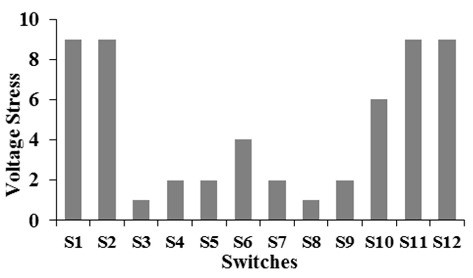
VS1 = VS2 = VS11 = VS12 = (V1 + V2 + V3) = 9 V
VS10 = V3 = 6 V
VS6 = (V3 − V2) = 4 V
VS4 = VS5 = VS7 = VS9 = V2 = 2 V
VS3 = VS8 = V1 = 1 V
The value of TSV will be
TSV = 2 × (V1) + 4 × (V2) + V3 + (V3 − V2) + 4 × (V1 + V2 + V3) = 56 V
The maximum voltage stress across each switch is shown in Figure 3. The TSV per unit provides a convenient and effective method for analyzing and comparing the impact of voltage stresses. It is the ratio of TSV to the maximum output voltage.
T S V p.u.   =   56   V 9   V =   6.22      
The proposed inverter achieves a slightly lower TSV. Importantly, most of the switches in the proposed circuit are subjected to relatively low blocking voltages (V, 2 V, or 4 V), and only a few devices are exposed to the full DC link stress. This favorable stress distribution enables the use of devices with lower voltage ratings for the majority of switches, thereby reducing conduction losses and overall inverter cost. The minimized TSV and selective use of high-voltage devices directly contribute to improved cost factor (CF) and efficiency of the proposed design.

2.3. Extended Generalized Structure

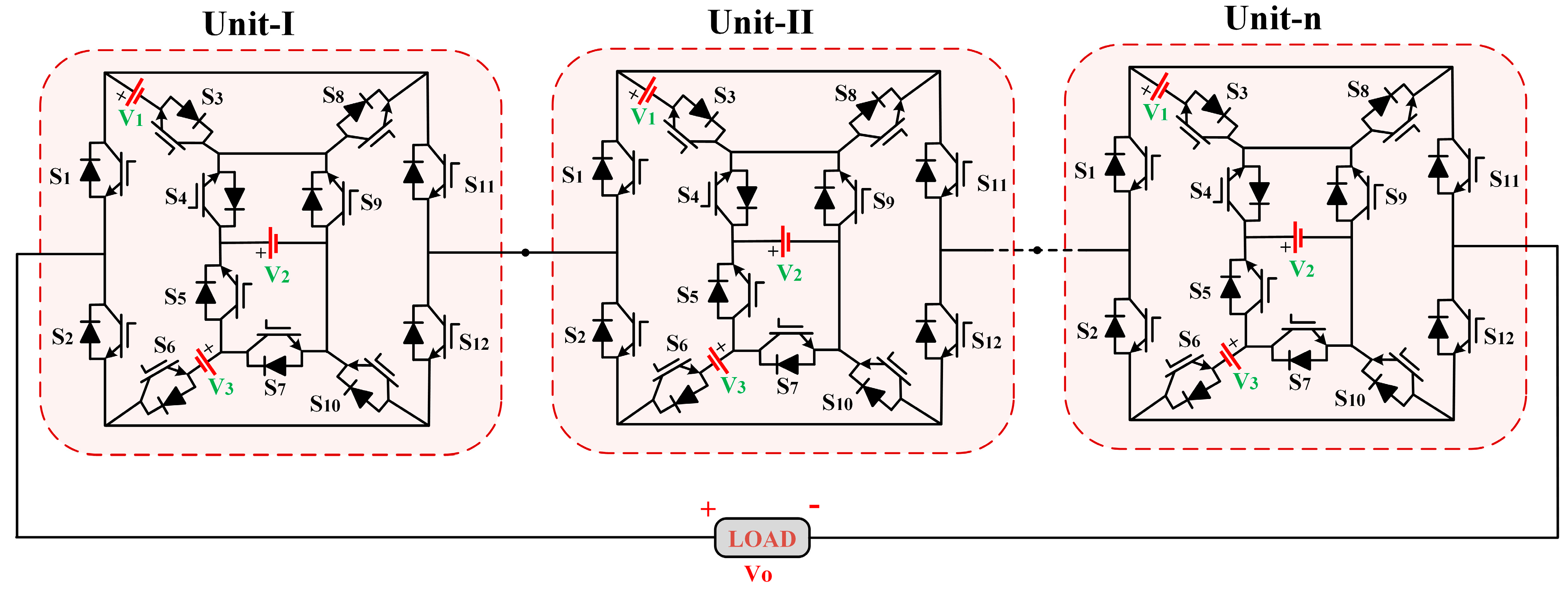
The proposed topology can be extended to achieve 19n-levels through cascaded operation. Its modular structure is shown in Figure 4. The total output voltage of the generalized structure, which is the sum of the voltages of all the basic units, can be written as
Vo = Vo,1 + Vo,2 + … + Vo,n
The relations for the generalized structure of the proposed topology for ‘n’ basic units are given as
NL = 19n
NIGBT = (NL − 7n)
NGD = (NL − 7n)
NDC = (NL − n)/6
where NL represents the number of output voltage levels, NIGBT is the number of IGBT switches, NGD is the number of gate driver circuits, and NDC is the number of DC sources, respectively.

2.4. Modulation Strategy

Modulation techniques control the output voltage waveform, reduce harmonics, improve efficiency, and achieve better output quality [23]. This work uses a low-frequency Nearest Level Control (NLC) PWM technique for the switching operation of the proposed converter. Compared with Selective Harmonic Elimination (SHE), which can eliminate specific low-order harmonics but requires complex offline computation of switching angles, NLC is simpler, scalable, and easier to implement in real time. High-frequency modulation techniques such as sinusoidal or level-shifted PWM, which require higher switching frequencies, incur larger switching losses. The implementation of NLC, shown in Figure 5a, involves a sinusoidal reference wave N × M × Sin(ωt) is compared against the discrete DC voltage levels, where N is the number of positive voltage levels and M is the modulation index. When the reference wave crosses the constant level, the switching state changes, causing the inverter output to step to the nearest available voltage level. Figure 5b illustrates how the continuous reference is quantized into discrete levels, and the resulting logic outputs are mapped to gate driver signals for the corresponding switches. This ensures that each transition of the reference produces a well-defined switching event, enabling the inverter to synthesize a low-THD AC waveform with minimal switching frequency [24,25].
The choice of NLC is particularly motivated by its benefits for renewable energy systems. First, it operates with a very low switching frequency, which minimizes switching losses and thermal stress on the semiconductor devices, thereby enhancing efficiency and prolonging device lifetime. This is critical in photovoltaic and wind energy systems, where converters are required to run continuously with high reliability. Second, despite the low switching frequency, the proposed 19-level inverter produces a high-resolution staircase waveform, which results in a low THD, satisfying IEEE 519 harmonic standards. Thus, NLC achieves both efficiency and power quality simultaneously. Third, NLC reduces implementation complexity, requiring simpler hardware and control logic compared to high-frequency PWM techniques, which is advantageous for modular renewable energy inverters.

2.5. Cost Analysis

The cost factor is a crucial aspect in selecting the most suitable multilevel inverter (MLI) for optimal affordability. Reducing the number of IGBTs (NIGBT), Driver Circuits (NGD), Capacitors (NC), Diodes (Nd), DC Sources (Ndc), and TSVp.u. significantly decreases the circuit’s cost and complexity. The cost factor (CF) is formulated as [26]
Cost Factor (CF) = NIGBT + NGD + NC + Nd + Ndc + αTSVp.u.
where α represents the weighting factor and determines the emphasis on switch ratings, with the CF value calculated for α = 0.5 and α = 1.5 for the proposed topology.
CF (α = 0.5) = 30.11,
CF per level (α = 0.5) = 30.11/19 = 1.58
CF (α = 1.5) = 36.33,
CF per level (α = 1.5) = 36.33/19 = 1.91

2.6. Reliability Analysis

Reliability refers to the ability of power electronic converter systems to consistently perform their functions over a specified period and under various operating conditions. As the number of devices in MLI increases, it leads to an increase in converter faults. According to an industry-based survey, capacitors and power electronic switches are the most susceptible to faults [27]. A fault-tolerant MLI with a high device count is expected to be less reliable. The researchers use the following terms to determine the reliability of converters: Failure rate (λ), and mean time to failure (MTTF) [28]. The failure rate is a reliability index representing the rate at which the converter fails. It helps to determine the probability of failure over a specified period. The MTTF refers to the average expected time until the occurrence of the first failure in the converter. MTTF has an inverse relation with the failure rate. Two methods are used to estimate the reliability, including device count and device stress [29]. The precise method for estimating the reliability of the converter is the device stress method, which considers different factors of operating conditions. In this method, the failure rate of different components is calculated and then added to determine the failure rate of a complete circuit. The parameters for MTTF calculation are derived from the MIL-HDBK 217E standard [25], shown in Table 2. Since the proposed topology consists only of switches, the failure rate of the switch (λs) can be calculated as follows:
λ s =   λ b π T π A π R π S π Q π E ·   ( F a i l u r e s / 10 6 · h )  
where λ b is the base failure rate of the device and π T is a temperature coefficient that can be expressed as
π T = e 2114 ( 1 T j + 273 1 298 )
where T j is the operating junction temperature of the switch that can be calculated as
T j = T c + θ j i P l o s s
where T c and θ j i are represented as ambient temperature and junction to case and case to ambient thermal resistance, respectively. Ploss is the power loss, discussed in Section 4. The term π A , π Q , and π E is represented as the application factor, quality factor, and environmental factor, respectively. The term πR is a power rating factor that has a relation with the power rating, P r of the switch and can be calculated as
π R = P r 0.37
Finally, the term π S is known as the voltage stress factor of the switch; it depends on Vs, which is the ratio of the applied collector-to-emitter voltage to the collector-to-emitter voltage in the OFF state of the switch. The π S can be estimated as
π s = 0.0045 e 3.1 V s
For the proposed topology, the calculated value of failure rate (λs) is 0.06216 Failures/hour, and the MTTF can be calculated as
  M T T F = 1 λ s = 16.08 · ( 10 6 × h o u r s / f a i l u r e )
The device failure rate and Mean Time to Failure (MTTF) are critical metrics for demonstrating the superiority of the proposed topology and optimizing its design. A lower failure rate indicates improved reliability, as it reduces component malfunction over time. A higher MTTF showcases the longevity of the proposed design. This indicates that the proposed topology can operate reliably for a longer duration before encountering failures. Furthermore, these reliability insights enable design optimization by guiding component selection, stress reduction, and thermal management techniques.

3. Results and Discussion

3.1. Simulation Results

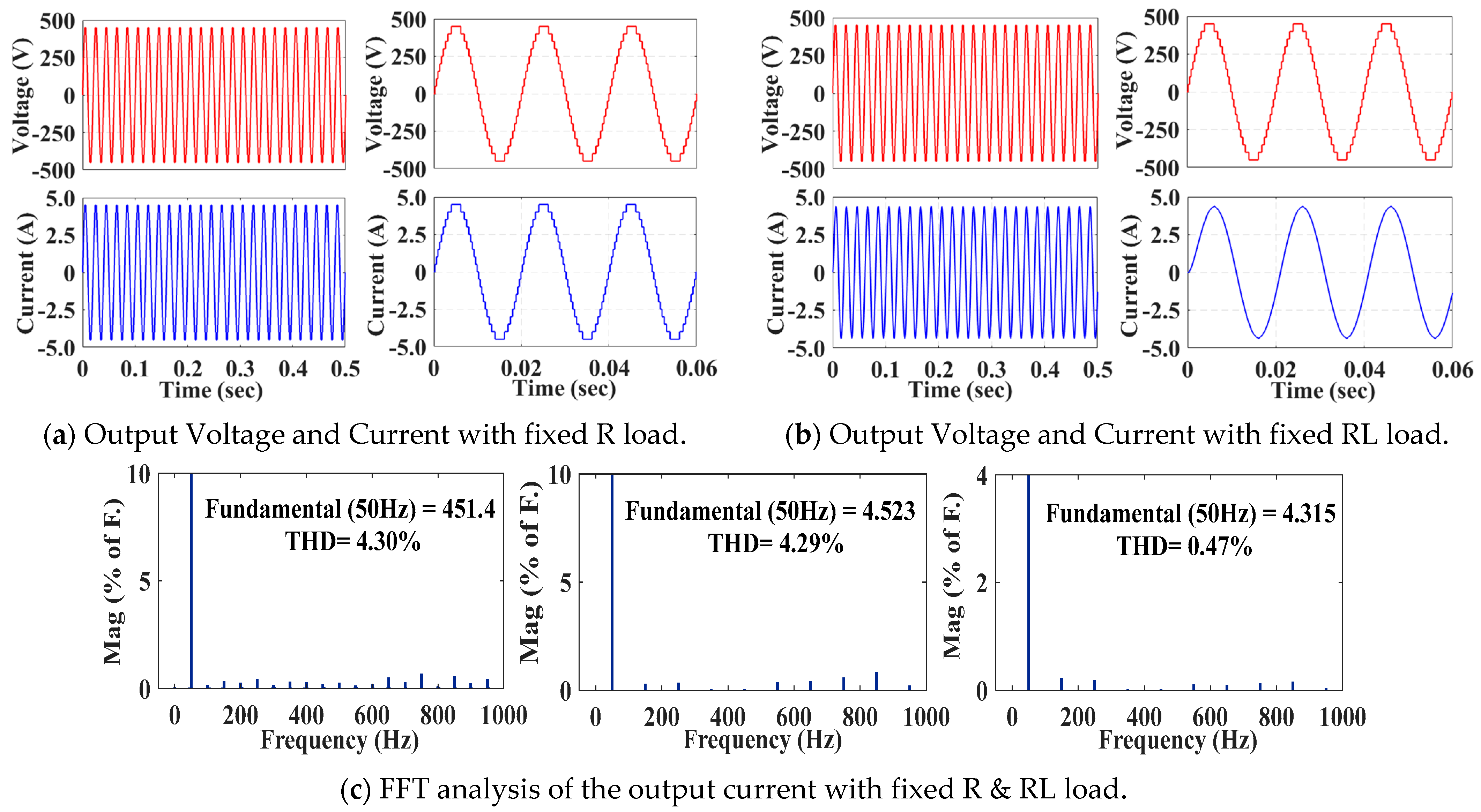
The proposed topology was simulated in MATLAB/Simulink for both static and dynamic loading conditions with the parameters listed in Table 3. The output voltage and current waveform are in phase for a fixed R of 100 Ω, as depicted in Figure 6a. The resultant output voltage waveform has a 19-level with a peak voltage of 450 V and a current waveform with a peak of 4.5 A. As the load changes to 100 Ω + 40 mH, the current waveform becomes sinusoidal, and a phase difference appears due to the inductive nature of the load shown in Figure 6b. The harmonic spectrum of output voltage and current is depicted in Figure 6c. The output voltage and current have a THD of 4.30% and 0.47%, respectively.
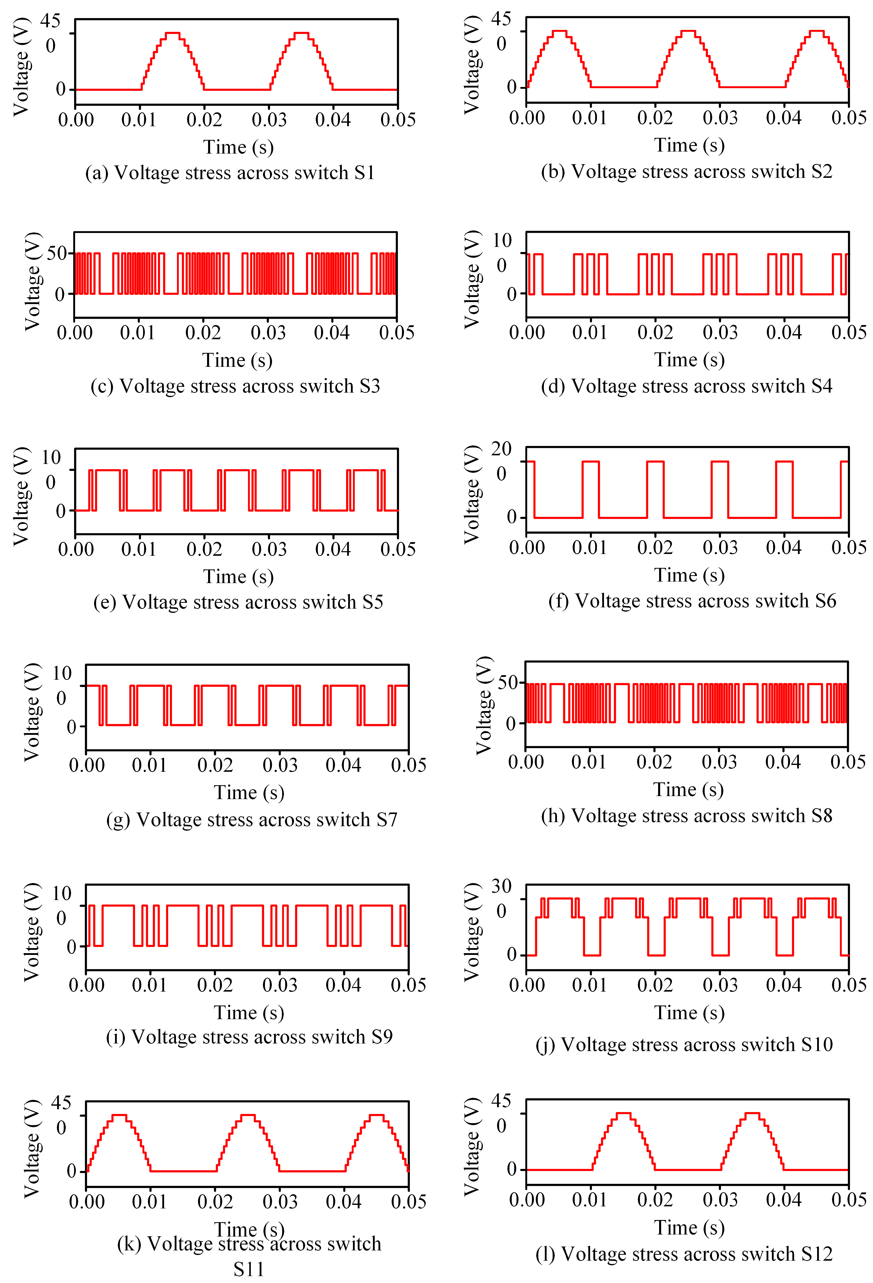
Load conditions in real-world scenarios can fluctuate dynamically due to various applications like industrial machinery operations, renewable energy systems, household use, and electric vehicles. The inverter’s stability was evaluated by simulating load transitions to ensure its reliability across various applications. The output voltage and current waveform for variable R form No-load to 100 Ω and then to 50 Ω are shown in Figure 7a. For dynamic change in RL load from No-load to 100 Ω + 40 mH and then to 50 Ω + 40 mH, the output voltage and current waveform are shown in Figure 7b. The proposed circuit operates well under both dynamic conditions, as evidenced by the change in current voltage. The waveforms for variable Power Factor (PF) are shown in Figure 7c. In certain cases, the modulation index of the converter could change due to faults or control system errors. To assess the dynamic stability of the converter, simulations were conducted for different modulation indices ranging from 1 to 0.8, and subsequently to 0.6. Upon transitioning from a modulation index of 1 to 0.8, the voltage levels decreased from 19 to 15. Further reducing the modulation index from 0.8 to 0.6 led to a subsequent decrease in voltage levels from 15 to 11. Figure 7d displays voltage and current waveforms for varying modulation index (MI). Figure 8 shows the voltage stress waveform across different switches.
It is important to note that reducing the MI decreases the number of available output levels, which increases the step size in the staircase waveform. This results in a higher harmonic content and an increase in the total harmonic distortion (THD) of the output voltage. While the proposed topology produces low THD (4.3%) at MI = 1, the THD rises as MI decreases, reflecting a trade-off between DC source utilization and power quality. In renewable energy applications, especially in grid-connected systems, this drawback can affect compliance with harmonic standards if MI is significantly reduced. However, even at MI = 0.6, the proposed inverter still provides 11 levels, ensuring that the waveform quality remains superior compared to conventional two-level or three-level inverters. Additionally, filtering and control strategies can be employed to mitigate the negative impact on power quality when operating at reduced MI.

3.2. Hardware Results

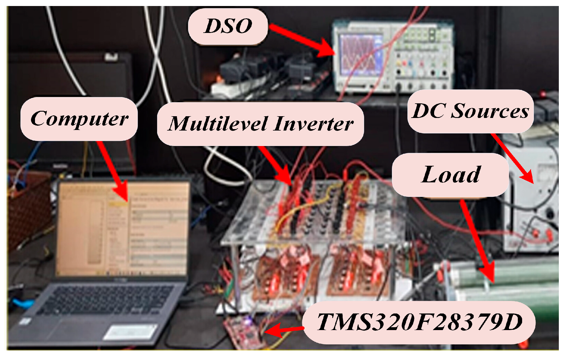
The practical feasibility of the proposed topology has been verified by developing a hardware prototype in the laboratory, shown in Figure 9. The experimental setup utilizes a TMS320F28379D DSP board for gate pulse generation, which provides the required PWM channels, an IGBT FGA25N120 for the power switch, and a TLP250H optocoupler IC for the gate driver circuit. The magnitude of the DC source voltages selected for hardware testing is 4.5 V, 9 V, and 27 V. The parameters used for experimental testing are shown in Table 4.
It is important to note that the hardware prototype employs a fundamental switching frequency of 50 Hz. This is because the NLC generates the staircase waveform directly at the fundamental frequency, avoiding high-frequency PWM switching. The main advantage of this approach is a substantial reduction in switching losses and thermal stress, which enhances efficiency and device lifetime. Although 50 Hz is considered low compared to conventional PWM inverters operating in the kHz range, the trade-off is justified for medium- and high-power renewable energy applications where efficiency is prioritized. Furthermore, future implementations could take advantage of wide-bandgap (WBG) devices such as SiC or GaN. These devices offer faster switching capability, lower switching losses, and improved thermal performance, which would allow higher-frequency operation while maintaining efficiency and enabling more compact passive components.
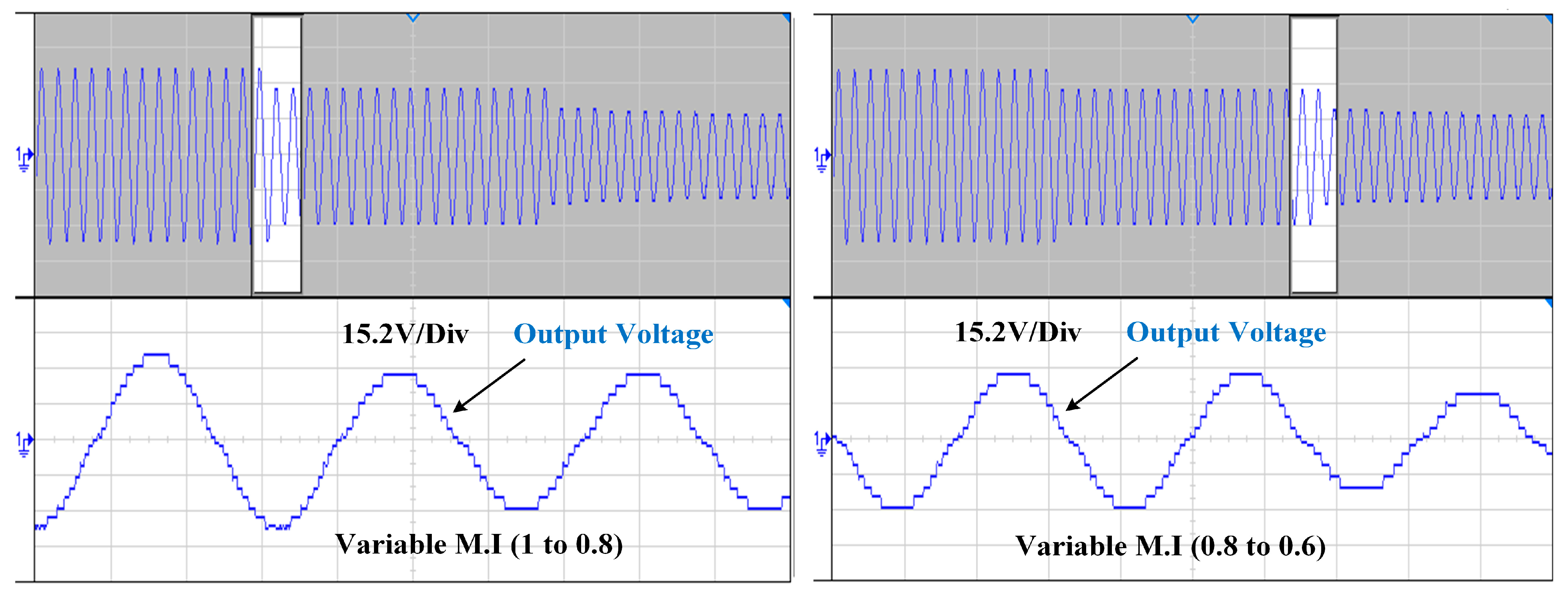
For a fixed resistive load of 40 Ω, the output voltage and current waveform are shown in Figure 10a, resulting in 19 levels of staircase output voltage. Figure 10b shows the output voltage and current waveform for a fixed RL load of 40 Ω + 90 mH. The output current becomes sinusoidal when the nature of the load is inductive. The proposed topology is also verified in experimental testing for dynamic changes in load. The proposed circuit successfully handles dynamically changing loads, as shown in Figure 10c,d. The output voltage and current waveforms show satisfactory performance for variable R load from 80 Ω to 40 Ω and variable RL load from 80 Ω + 90 mH to 40 Ω + 120 mH. The topology is also varied for dynamic change in the modulation index (MI) from 1 to 0.8 and then 0.6, as shown in Figure 11.

4. Power Loss Analysis

Power loss analysis is crucial for designing topologies as it directly impacts converter efficiency and generates heat within components, leading to component degradation, reduced lifespan, and even failure. A power electronic switch operates in three modes: blocking mode, conduction mode, and switching mode. However, there are negligible losses in blocking mode. Therefore, losses mainly occur during switching mode and conduction mode. Switching losses occur during the transitions of the semiconductor devices in the converter, including turn-on and turn-off losses. Conduction losses occur when current flows through the ON-state semiconductor devices. These losses of IGBTs with antiparallel diodes are due to on-state voltage drop and turn-on resistance. These losses increase with the number of switches in the conduction state. Conduction losses (Pc) are more pronounced at low switching frequencies. The following equations can be used for the estimation of losses [25].
P c , I G B T = V O N , I G B T i t + R I G B T i β ( t )
P c , D i o d e = V O N , D i o d e i t + R D i o d e i 2 ( t )
where V O N , I G B T and V O N , D i o d e represent the ON-state voltage drops of the IGBT and antiparallel diode, respectively. R I G B T and R D i o d e denote the equivalent resistances of the IGBT and the diode, and i(t) is the conduction current. The term β is a constant determined by the datasheet of the switch. The total conduction losses of the converter can be estimated as
P c = j = 1 N I G B T 1 2 π 0 2 π V O N , I G B T , j i t + R I G B T i β t d t + k = 1 N D i o d e 1 2 π 0 2 π V O N , D i o d e , k i t + R D i o d e i 2 t d t
Switching losses arise due to the delay in the time transition of switches. Ideally, the switch should instantaneously change its state, but practically, it takes a small duration to change its state, causing energy dissipation in the form of heat. These losses are higher at high switching frequencies. Assuming the variation in voltage and current to be linear during the transition, the switching loss (Psw) for the fundamental frequency, f, can be determined by the given equation [30]:
P s w = k = 1 N s w E O N , k T O N , k + E O F F , k T O F F , k × f
Here, EON,k and EOFF,k represents the energy loss during turn-on and turn-off in one cycle for the kth IGBT and diode, respectively. TON,k and TOFF,k indicate the number of turn-on and turn-off cycles for the kth IGBT and diode, respectively. Now, total losses PTotal Loss are given by
PTotal Loss = Pc + Psw
The efficiency of the converter gives an idea about its performance and can be calculated using the equation:
η = P o u t P o u t + P T o t a l L o s s × 100 %
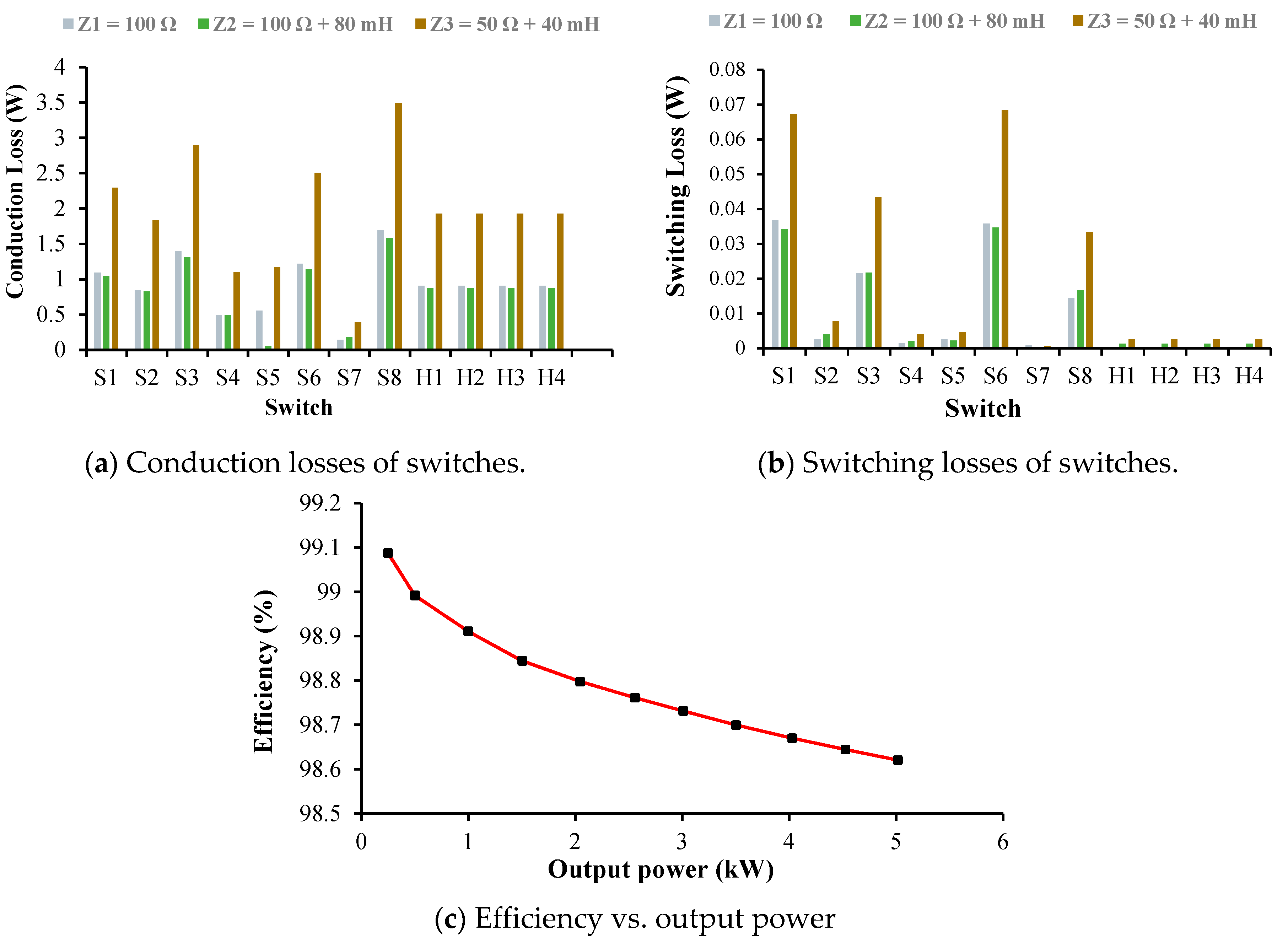
Thermal modeling was conducted using PLECS 4.1.2 software, utilizing IGBT/diode IKW75N65EL5 manufactured by Infineon. The manufacturer’s datasheet provides multi-dimensional lookup tables for accurately calculating losses in power semiconductor devices. The conduction and switching losses were evaluated for three different loading conditions, as shown in Figure 12a,b. The results indicate that switching losses are smaller than conduction losses since the circuit was implemented using a low switching frequency. Figure 12c shows the variation in efficiency with output power. The proposed converter achieves a maximum efficiency of 98.08% at an output voltage of 250 W.

5. Comparative Analysis

This section presents a comparative evaluation of the proposed topology with several reported asymmetrical multilevel topologies. The comparison considers the number of output levels (NL), number of IGBTs (NIGBT), number of gate drivers (Ngd), number of capacitors (NC), number of DC sources (Ndc), per-unit Total Standing Voltage (TSVp.u.), cost factor per level (CF/NL) for α = 0.5 and α = 1.5, and NIGBT/NL. These parameters jointly determine the technical and economic suitability of an inverter topology. Table 5 highlights that asymmetrical topologies with 17 levels [31,32,33,34] employ a relatively large device count and generally exhibit higher TSV values. Such characteristics increase complexity, cost, and switching losses, limiting their practical scalability. In contrast, more recent designs such as [35,36] with 21 levels demonstrate improved performance: [35] reduces NIGBT/NL but requires 7 DC sources, which complicates implementation, whereas [36] achieves an excellent TSVp.u. value of 4.0 along with favorable CF/NL, but still relies on 6 DC sources. Thus, while [36] is attractive from a voltage stress perspective, its need for additional sources increases system cost and limits compactness. For 19-level inverters, topologies in [37,38] use 18 switches, leading to a high device-per-level ratio (0.94) and higher CF, though they achieve lower TSVp.u. compared to our design. The topology in [39] offers a lower NIGBT/NL (0.57) and competitive CF/NL, but this comes at the expense of requiring five DC sources and incurring a relatively high TSVp.u. value of 6.25.
The proposed topology, generating 19 levels with only 12 switches and 3 DC sources, achieves a favorable balance across all metrics. Its NIGBT/NL ratio (0.63) and CF/NL (1.58–1.91) compare well against alternatives, while its TSVp.u. of 6.22 remains acceptable for practical device ratings. Although not the lowest TSV reported, the distribution of voltage stress, where most switches experience lower voltages (V, 2 V, or 4 V) enables the use of lower-rated and lower-cost devices for the majority of switches. This reduces conduction losses and improves overall efficiency.
In summary, the comparison reveals that no single topology dominates across all parameters. Designs like [36] excel in TSV reduction but require more DC sources, while others, such as [39], reduce the switch-to-level ratio but incur higher voltage stress. The strength of the proposed topology lies in offering a compact, modular, and cost-effective structure with reduced device count, competitive TSV, and low-cost factor, making it especially well-suited for renewable energy applications where simplicity, efficiency, and scalability are key priorities.

6. Application of the Proposed Topology

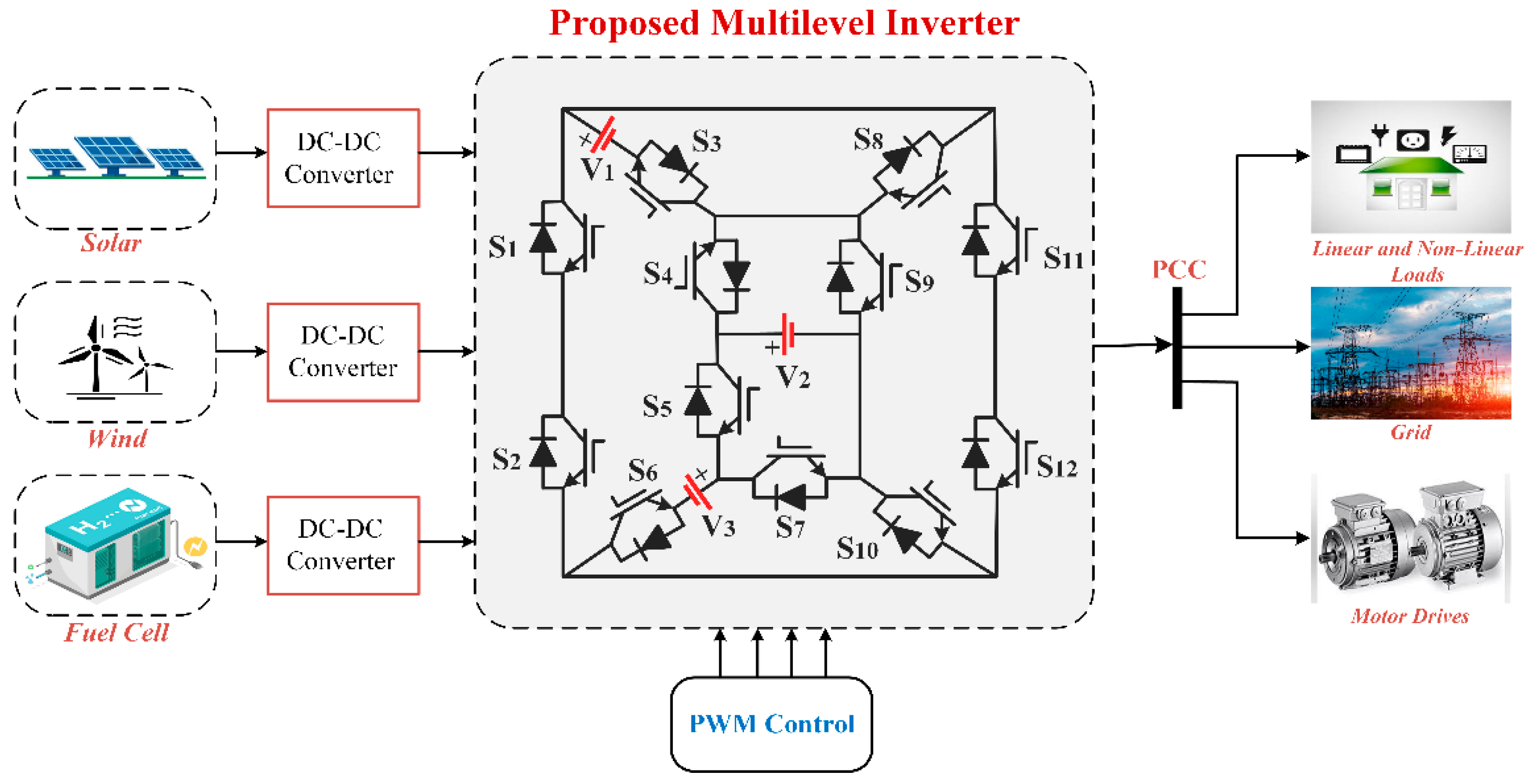
The proposed inverter topology is a key component in enhancing the efficiency and integration of renewable energy systems. It provides a flexible and reliable power supply by enabling the simultaneous connection of renewable energy sources like solar panels, wind turbines, and fuel cells, as shown in Figure 13. They convert the direct current (DC) from these sources into high-quality alternating current (AC) with multiple voltage levels, reducing harmonics and improving power quality. This is particularly beneficial for grid-connected systems, where the inverter can stabilize the power supply and improve overall efficiency [40]. In standalone systems, especially in remote areas without grid access, the proposed topology can combine different renewable sources to ensure a consistent power supply. Additionally, the proposed topology is essential in smart grids and electric vehicle charging stations [41,42,43]. The proposed converter optimizes the use of available renewable energy and reduces dependence on conventional power sources [44,45,46]. Despite challenges [47,48,49] such as complexity and cost, the benefits of improved power quality, scalability, and efficient energy management make the proposed topology a vital component in advancing renewable energy integration.

7. Conclusions

This paper presents an improved structure of a single-phase asymmetrical multilevel inverter topology with extension capability to produce higher levels in the output voltage waveforms. The proposed topology generates 19 levels at the output by using 12 unidirectional switches and 3 DC sources. The proposed MLI topology is thoroughly analyzed, and its performance is evaluated using MATLAB/Simulink and verified experimentally under different loading conditions. The proposed converter achieved a THD of 4.3% in output voltage, which complies with the IEEE 519 harmonic standard, ensuring high power quality. To demonstrate the practical applicability of the proposed topology for renewable energy applications. The dynamic performance under varying load conditions highlights its stability and reliability. The reliability analysis of the proposed topology reveals a higher mean time to fault value (MTTF), indicating robustness and suitability for long-term operation. Additionally, the power loss analysis shows a maximum efficiency of 99.08% with a detailed distribution of losses across all switches under different loading conditions. The results confirm that the proposed topologies offer high efficiency, low harmonic distortion, and robust performance under different loading conditions, making them a promising solution for various renewable energy applications.

Author Contributions

Conceptualization, M.F.A. and M.S.B.A.; methodology, A.B.; software, A.W.; validation, M.F.A. and A.B.; formal analysis, A.W.; writing—original draft preparation, A.B. and M.F.A.; writing—review and editing, M.F.A., M.S.B.A. and M.A.; supervision, M.S.B.A., J.R. and M.A. All authors have read and agreed to the published version of the manuscript.

Funding

Supported by ANID through projects FB0008, 1210208, and 1221293.

Data Availability Statement

No new data were created or analyzed in this study.

Acknowledgments

J. Rodriguez acknowledges the support of ANID FB0008, 1210208, and 1221293.

Conflicts of Interest

The authors declare that this study received funding from ANID. The funder was not involved in the study design, collection, analysis, interpretation of data, the writing of this article, or the decision to submit it for publication.

References

  1. Rodriguez, J.; Franquelo, L.G.; Kouro, S.; Leon, J.I.; Portillo, R.C.; Prats, M.A.M.; Perez, M.A. Multilevel Converters: An Enabling Technology for High-Power Applications. IEEE Proc. 2009, 97, 1786–1817. [Google Scholar] [CrossRef]
  2. Barzegarkhoo, R.; Forouzesh, M.; Lee, S.S.; Blaabjerg, F.; Siwakoti, Y.P. Switched-Capacitor Multilevel Inverters: A Comprehensive Review. IEEE Trans. Power Electron. 2022, 37, 11209–11243. [Google Scholar] [CrossRef]
  3. Mukundan, N.; Sangeetha, V.; Jayaprakash, P.; Asokan, O.V.; Al-Durra, A.; Zeineldin, H.; El-Fouly, T.H. A New Multilevel Inverter Based Grid Connected Reliable Solar Power Transfer Unit with Power Quality Enhancement. IEEE Trans. Ind. Appl. 2023, 59, 1887–1900. [Google Scholar] [CrossRef]
  4. Anand, V.; Singh, V.; Mekhlief, S. Power electronics for renewable energy systems. Renew. Energy Sustain. Growth Assess. 2022, 5, 81–117. [Google Scholar]
  5. Ramasamy, S.; Sivasubramaniyam, V.; Gatto, G.; Kumar, A. DC link voltage control based energy management strategy for standalone solar PV fed hybrid system. In Proceedings of the 2023 AEIT International Conference on Electrical and Electronic Technologies for Automotive (AEIT AUTOMOTIVE), Modena, Italy, 17–19 July 2023; IEEE: Piscataway, NY, USA, 2023. [Google Scholar]
  6. Rajender, B. A dissertation submitted in partial fulfillment of the requirements for the award of the degree of Master of Technology in Electrical Engineering with specialization in Electric Drives and Power Electronics. Indian Inst. Technol. Roorkee 2011. [Google Scholar]
  7. Akbari, A.; Ebrahimi, J.; Jafarian, Y.; Bakhshai, A. A Multilevel Inverter Topology with an Improved Reliability and a Reduced Number of Components. IEEE J. Emerg. Sel. Top. Power Electron. 2022, 10, 553–563. [Google Scholar] [CrossRef]
  8. Gupta, K.K.; Ranjan, A.; Bhatnagar, P.; Sahu, L.K.; Jain, S. Multilevel inverter topologies with reduced device count: A review. IEEE Trans. Power Electron. 2016, 31, 135–151. [Google Scholar] [CrossRef]
  9. Vemuganti, H.P.; Sreenivasarao, D.; Ganjikunta, S.K.; Suryawanshi, H.M.; Abu-Rub, H. A survey on reduced switch count multilevel inverters. IEEE Open J. Ind. Electron. Soc. 2021, 2, 80–111. [Google Scholar] [CrossRef]
  10. Samadaei, E.; Sheikholeslami, A.; Gholamian, S.A.; Adabi, J. A Square T-Type (ST-Type) Module for Asymmetrical Multilevel Inverters. IEEE Trans. Power Electron. 2018, 33, 987–996. [Google Scholar] [CrossRef]
  11. Samadaei, E.; Kaviani, M.; Bertilsson, K. A 13-levels module (K-type) with two DC sources for multilevel inverters. IEEE Trans. Ind. Electron. 2019, 66, 5186–5196. [Google Scholar] [CrossRef]
  12. Ounejjar, Y.; Al-Haddad, K.; Gregoire, L.-A. Packed U cells multilevel converter topology: Theoretical study and experimental validation. IEEE Trans. Ind. Electron. 2011, 58, 1294–1306. [Google Scholar]
  13. Gupta, K.K.; Jain, S. A novel multilevel inverter based on switched DC sources. IEEE Trans. Ind. Electron. 2014, 61, 3269–3278. [Google Scholar]
  14. Nair, R.V.; Gopakumar, K.; Franquelo, L.G. A Very High Resolution Stacked Multilevel Inverter Topology for Adjustable Speed Drives. IEEE Trans. Ind. Electron. 2018, 65, 2049–2056. [Google Scholar] [CrossRef]
  15. Jena, K.; Kumar, D.; Kumar, B.H.; Janardhan, K.; Singh, A.R.; Naidoo, R.; Bansal, R.C. A Single DC Source Generalized Switched Capacitors Multilevel Inverter with Minimal Component Count. Int. Trans. Electr. Energy Syst. 2023, 2023, 3945160. [Google Scholar] [CrossRef]
  16. Kumari, M.; Siddique, M.D.; Sarwar, A.; Tariq, M.; Mekhilef, S.; Iqbal, A. Recent trends and review on switched-capacitor-based singlestage boost multilevel inverter. Int. Trans. Elect. Energy Syst. 2021, 31, 3. [Google Scholar] [CrossRef]
  17. Behara, S.; Sandeep, N.; Yaragatti, U.R. Design and Implementation of Transformer-Based Multilevel Inverter Topology with Reduced Components. IEEE Trans. Ind. Appl. 2018, 54, 4632–4639. [Google Scholar] [CrossRef]
  18. Thangapandi, A.K.; Kumar, A.; Karthigeyan, D.; Ramasamy, S.; Arumugam, V.; Gatto, G. A novel artificial neural network based selection harmonic reduction technique for single source fed high gain switched capacitor coupled multilevel inverter for renewable energy applications. Heliyon 2024, 10, 19. [Google Scholar] [CrossRef]
  19. Thiyagarajan, V.; Somasundaram, P. Simulation of New Symmetric and Asymmetric Multilevel Inverter Topology with Reduced Number of Switches. In Proceedings of the 2018 4th International Conference on Electrical Energy Systems (ICEES), Chennai, India, 7–9 February 2018; pp. 315–319. [Google Scholar]
  20. Siddique, M.D.; Mustafa, A.; Sarwar, A.; Mekhilef, S.; Shah, N.B.M.; Seyedamahmousian, M.; Stojcevski, A.; Horan, B.; Ogura, K. Single phase symmetrical and asymmetrical design of multilevel inverter topology with reduced number of switches. In Proceedings of the 2018 IEEMA Engineer Infinite Conference, New Delhi, India, 13–14 March 2018; IEEE: Piscataway, NY, USA, 2018; pp. 1–6. [Google Scholar]
  21. Barzegarkhoo, R.; Moradzadeh, M.; Zamiri, E.; Kojabadi, H.M.; Blaabjerg, F. A new boost switched-capacitor multilevel converter with reduced circuit devices. IEEE Trans. Power Electron. 2018, 33, 6738–6754. [Google Scholar] [CrossRef]
  22. Arif, M.S.B.; Mustafa, U.; Ayob, S.B.M.; Rodriguez, J.; Nadeem, A.; Abdelrahem, M. Asymmetrical 17-Level inverter topology with reduced total standing voltage and device count. IEEE Access 2021, 9, 69710–69723. [Google Scholar] [CrossRef]
  23. Shehu, G.S.; Kunya, A.B.; Shanono, I.H.; Yalçınöz, T.A. Review of Multilevel Inverter Topology and Control Techniques. Int. J. Autom. Control. 2016, 4, 233–241. [Google Scholar] [CrossRef]
  24. Sarwer, Z.; Sarwar, A.; Zaid, M.; Hussan, M.R.; Tariq, M.; Alamri, B.; Alahmadi, A. Implementation of a Novel Variable Structure Nearest Level Modulation on Cascaded H-Bridge Multilevel Inverter. IEEE Access 2021, 9, 133974–133988. [Google Scholar] [CrossRef]
  25. Ahmad, M.F.; Arif, M.S.B.; Abdelrahem, M.; Rodriguez, J. A high gain and compact size asymmetrical 17-level inverter for medium-and high-power applications. Int. J. Circuit Theory Appl. 2023, 52, 2741–2759. [Google Scholar] [CrossRef]
  26. Mustafa, U.; Arif, M.S.B.; Kennel, R.; Abdelrahem, M. Asymmetrical eleven-level inverter topology with reduced power semiconductor switches total standing voltage and cost factor. IET Power Electron. 2022, 15, 395–411. [Google Scholar] [CrossRef]
  27. Yang, S.; Bryant, A.; Mawby, P.; Xiang, D.; Ran, L.; Tavner, P. An Industry Based Survey of Reliability in Power Electronic Converters. IEEE Trans. Ind. Appl. 2011, 47, 1441–1451. [Google Scholar] [CrossRef]
  28. Alavi, O.; Hooshmand Viki, A.; Shamlou, S. A Comparative Reliability Study of Three Fundamental Multilevel Inverters Using Two Different Approaches. Electronics 2016, 5, 18. [Google Scholar] [CrossRef]
  29. US Department of Defense. US Department of Defense: MIL-HDBK-217F (NOTICE 2), Military Handbook Reliability Prediction of Electronic Equipment; Defense Technical Information Center: Alexandria, VI, USA, 1995. [Google Scholar]
  30. Thakre, K.; Mohanty, K.B.; Chatterjee, A.; Kommukuri, V.S. A modified circuit for symmetric and asymmetric multilevel inverter with reduced components count. Int. Trans. Electr. Energy Syst. 2019, 29, e12011. [Google Scholar] [CrossRef]
  31. Alishah, R.S.; Hosseini, S.H.; Babaei, E.; Sabahi, M. A new general multilevel converter topology based on cascaded connection of submultilevel units with reduced switching components, DC sources, and blocked voltage by switches. IEEE Trans. Ind. Electron. 2016, 63, 7157–7164. [Google Scholar] [CrossRef]
  32. Ngo, B.; Nguyen, M.; Kim, J.; Zare, F. Single-phase multilevel inverter based on switched-capacitor structure. IET Power Electron. 2018, 11, 1858–1865. [Google Scholar] [CrossRef]
  33. Dhanamjayulu, C.; Prasad, D.; Padmanaban, S.; Maroti, P.K.; Holm-Nielsen, J.B.; Blaabjerg, F. Design and implementation of seventeen level inverter with reduced components. IEEE Access. 2021, 9, 16746–16760. [Google Scholar] [CrossRef]
  34. Seifi, A.; Hosseini, S.H.; Hagh, M.T.; Hosseinpour, M. New multilevel inverter based on reduced switch basic cell for high voltage levels. IET Power Electron. 2024, 17, 551–563. [Google Scholar] [CrossRef]
  35. Babaei, E.; Laali, S.; Bayat, Z. A Single-Phase Cascaded Multilevel Inverter Based on a New Basic Unit with Reduced Number of Power Switches. IEEE Trans. Ind. Electron. 2015, 62, 922–929. [Google Scholar]
  36. Meraj, S.T.; Yahaya, N.Z.; Hasan, K.; Masaoud, A. Single phase 21 level hybrid multilevel inverter with reduced power components employing low frequency modulation technique. Int. J. Power Electron. Drive Syst. 2020, 11, 810. [Google Scholar]
  37. Dargahi, V.; Sadigh, A.K.; Abarzadeh, M.; Pahlavani, M.R.A.; Shoulaie, A. Flying capacitor reduction in an improved double flying capacitor multicell converter controlled by a modified modulation method. IEEE Trans. Power Electron. 2012, 27, 3875–3887. [Google Scholar] [CrossRef]
  38. Babaei, E.; Laali, S.; Alilu, S. Cascaded Multilevel Inverter with Series Connection of Novel H-Bridge Basic Units. IEEE Trans. Ind. Electron. 2014, 61, 6664–6671. [Google Scholar] [CrossRef]
  39. Hosseini Montazer, B.; Olamaei, J.; Hosseinpour, M.; Mozafari, B. A generalized diode containing bidirectional topology for multilevel inverter with reduced switches and power loss. Int. J. Circ. Theor. Appl. 2021, 49, 2959–2978. [Google Scholar] [CrossRef]
  40. Bana, P.R.; Panda, K.P.; Naayagi, R.T.; Siano, P.; Panda, G. Recently developed reduced switch multilevel inverter for renewable energy integration and drives application: Topologies, comprehensive analysis and comparative evaluation. IEEE Access 2019, 7, 54888–54909. [Google Scholar] [CrossRef]
  41. Mittal, S.; Singh, A.; Chittora, P. Design and development of Reduced Switch Five Level Inverter for interfacing renewable energy sources and EV charger. Electr. Eng. 2024, 107, 6735–6749. [Google Scholar] [CrossRef]
  42. Zhang, R.; Wang, S.; Ma, J.; Jiang, Y.; Wang, P.; Liu, T.; Yang, Y. An Asymmetric Hybrid Phase-Leg Modular Multilevel Converter with Small Volume, Low Cost, and DC Fault-Blocking Capability. IEEE Trans. Power Electron. 2025, 40, 5336–5351. [Google Scholar] [CrossRef]
  43. Gao, S.; Chen, Y.; Song, Y.; Yu, Z.; Wang, Y. An Efficient Half-Bridge MMC Model for EMTP-Type Simulation Based on Hybrid Numerical Integration. IEEE Trans. Power Syst. 2024, 39, 1162–1177. [Google Scholar] [CrossRef]
  44. Rong, Q.; Hu, P.; Yu, Y.; Wang, D.; Cao, Y.; Xin, H. Virtual External Perturbance-Based Impedance Measurement of Grid-Connected Converter. IEEE Trans. Ind. Electron. 2025, 72, 2644–2654. [Google Scholar] [CrossRef]
  45. Rong, Q.; Hu, P.; Wang, L.; Li, Y.; Yu, Y.; Wang, D.; Cao, Y. Asymmetric Sampling Disturbance-Based Universal Impedance Measurement Method for Converters. IEEE Trans. Power Electron. 2024, 39, 15457–15461. [Google Scholar] [CrossRef]
  46. Zhang, J.; Li, H.; Kong, X.; Zhou, J.; Shi, G.; Zang, J.; Wang, J. A Novel Multiple-Medium-AC-Port Power Electronic Transformer. IEEE Trans. Ind. Electron. 2024, 71, 6568–6578. [Google Scholar] [CrossRef]
  47. Li, N.; Zhang, C.; Liu, Y.; Zhuo, C.; Liu, M.; Yang, J.; Zhang, Y. Single-Degree-of-Freedom Hybrid Modulation Strategy and Light-Load Efficiency Optimization for Dual-Active-Bridge Converter. IEEE J. Emerg. Sel. Top. Power Electron. 2024, 12, 3936–3947. [Google Scholar] [CrossRef]
  48. Li, S.; Zhou, J.; Zhou, F.; Niu, F.; Deng, W. A Reduced Current Ripple Overmodulation Strategy for Indirect Matrix Converter. IEEE Trans. Ind. Electron. 2025, 72, 3768–3777. [Google Scholar] [CrossRef]
  49. Lu, G.; Lin, Q.; Zheng, D.; Zhang, P. Online Degradation Fault Prognosis for DC-Link Capacitors in Multistring-Connected Photovoltaic Boost Converters Subject to Cable Uncertainties. IEEE J. Emerg. Sel. Top. Power Electron. 2025, 13, 1107–1117. [Google Scholar] [CrossRef]
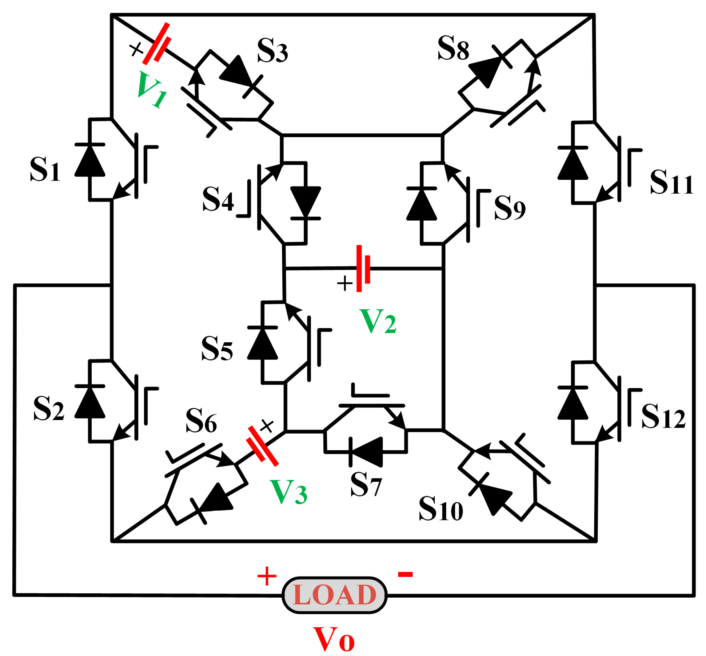
Figure 1. Proposed 19-level asymmetrical inverter topology.
Energies 18 05121 g001
Figure 2. Current conduction path of the proposed topology during a positive half cycle.
Energies 18 05121 g002
Figure 3. Maximum voltage stress of switches.
Energies 18 05121 g003
Figure 4. Generalized structure of the proposed topology.
Energies 18 05121 g004
Figure 5. (a) Method to generate levels from NLC and (b) Staircase sinusoidal output from NLC.
Energies 18 05121 g005
Figure 6. Simulation results with fixed loading conditions.
Energies 18 05121 g006
Figure 7. Simulation results with dynamic loading conditions.
Energies 18 05121 g007
Figure 8. Voltage stress across different switches.
Energies 18 05121 g008
Figure 9. Experimental setup of the proposed topology.
Energies 18 05121 g009
Figure 10. Hardware results under fixed and dynamic loading conditions.
Energies 18 05121 g010
Figure 11. Hardware results under a change in modulation index from 1 to 0.8 and then to 0.6.
Energies 18 05121 g011
Figure 12. Power losses and efficiency for different loading conditions.
Energies 18 05121 g012
Figure 13. Application of the proposed multilevel inverter topology.
Energies 18 05121 g013
Table 1. Switching states of the proposed topology.
VoSwitches States
S1S2S3S4S5S6S7S8S9S10S11S12
+1 V101000001101
+2 V100100010101
+3 V101100000101
+4 V100011011001
+5 V101011001001
+6 V100001111001
+7 V101111000001
+8 V100101110001
+9 V101101100001
0 V100000011101
−1 V011110100110
−2 V010100010110
−3 V011100000110
−4 V010011011010
−5 V011011001010
−6 V010001111010
−7 V011111000010
−8 V010101110010
−9 V011101100010
Table 2. Parameters for MTTF calculation (MIL-HDBK 217E standard).
ParametersValues
λ b 0.00074
θjc1 °C/W
θca64 °C/W
Ta30 °C/W
π A 1.5
π Q 1
π E 1
π S R 1
Vs0.6
Table 3. Simulation Parameters.
ParametersValues
VoltagesV1 = 50 V, V2 = 100 V, V3 = 300 V
Switching frequency50 Hz
SwitchIGBT
Resistive load50 Ω, 100 Ω
Inductive load40 mH, 80 mH
Modulation index (MI)1, 0.8, 0.6
Table 4. Experimental Parameters.
Parameters/DeviceValues
DC source voltagesV1 = 4.5 V, V2 = 9 V, V3 = 27 V
Switching frequencyNLC-PWM @ 50 Hz
SwitchIGBT/FGA25N120/1200 V, 25 A
ControllerTMS320F28379D
Gate Driver ICTLP250H
Resistive load40 Ω, 80 Ω
Inductive load90 mH, 120 mH
Modulation index (MI)1, 0.8, 0.6
Table 5. Comparison with other asymmetrical topologies.
TopologyNLNIGBTNIGBT/NLNgdNdcTSVp.u.NCCF/NL (α = 0.5)CF/NL (α = 1.5)
[31]17120.70104601.72.05
[32]17120.701226.631.92.28
[33]17160.941446.542.422.8
[34]17181.051886.502.773.16
[31]17120.70104601.692.05
[35]21160.761676.702.012.33
[36]21100.47106401.331.52
[37]19180.941824.942.332.59
[38]19180.94186402.312.52
[39]19110.571056.2501.531.86
Proposed19120.631236.2201.581.91
Disclaimer/Publisher’s Note: The statements, opinions and data contained in all publications are solely those of the individual author(s) and contributor(s) and not of MDPI and/or the editor(s). MDPI and/or the editor(s) disclaim responsibility for any injury to people or property resulting from any ideas, methods, instructions or products referred to in the content.