Article

Solid-State Circuit Breaker Topology Design Methodology for Smart DC Distribution Grids with Millisecond-Level Self-Healing Capability

1
School of Electrical and Automation Engineering, East China Jiaotong University, Nanchang 330013, China
2
State Grid Jiangxi Electric Power Co., Ltd., Electric Power Science Research Institute, Nanchang 330013, China
*
Author to whom correspondence should be addressed.
Energies 2025, 18(14), 3613; https://doi.org/10.3390/en18143613
Submission received: 17 June 2025 / Revised: 2 July 2025 / Accepted: 4 July 2025 / Published: 9 July 2025
(This article belongs to the Special Issue AI Solutions for Energy Management: Smart Grids and EV Charging)

Abstract

To address the challenges of prolonged current isolation times and high dependency on varistors in traditional flexible short-circuit fault isolation schemes for DC systems, this paper proposes a rapid fault isolation circuit design based on an adaptive solid-state circuit breaker (SSCB). By introducing an adaptive current-limiting branch topology, the proposed solution reduces the risk of system oscillations induced by current-limiting inductors during normal operation and minimizes steady-state losses in the breaker. Upon fault occurrence, the current-limiting inductor is automatically activated to effectively suppress the transient current rise rate. An energy dissipation circuit (EDC) featuring a resistor as the primary energy absorber and an auxiliary varistor (MOV) for voltage clamping, alongside a snubber circuit, provides an independent path for inductor energy release after faults. This design significantly alleviates the impact of MOV capacity constraints on the fault isolation process compared to traditional schemes where the MOV is the primary energy sink. The proposed topology employs a symmetrical bridge structure compatible with both pole-to-pole and pole-to-ground fault scenarios. Parameter optimization ensures the IGBT voltage withstand capability and energy dissipation efficiency. Simulation and experimental results demonstrate that this scheme achieves fault isolation within 0.1 ms, reduces the maximum fault current-to-rated current ratio to 5.8, and exhibits significantly shorter isolation times compared to conventional approaches. This provides an effective solution for segment switches and tie switches in millisecond-level self-healing systems for both low-voltage (LVDC, e.g., 750 V/1500 V DC) and medium-voltage (MVDC, e.g., 10–35 kV DC) smart DC distribution grids, particularly in applications demanding ultra-fast fault isolation such as data centers, electric vehicle (EV) fast-charging parks, and shipboard power systems.

1. Introduction

Fault self-healing in intelligent distribution networks is a key technology for smart grids [1]. As a crucial component of smart grids, flexibly interconnected DC distribution networks rely on the rapid operation of section switches and tie switches within the DC network to achieve efficient reconfiguration of load transfer paths and the formation of planned islands [2,3,4]. However, traditional circuit breaker-based section and tie switches are incapable of achieving millisecond-level fault self-healing in intelligent distribution networks. Therefore, there is an urgent need to research novel DC circuit breaker topologies to enable rapid circuit closing and breaking actions [5,6,7].
Achieving fast operation in DC circuit breakers primarily involves addressing the following two challenges:
1. Adaptive connection of current-limiting components: Direct installation of inductor-based current limiters in the main circuit can cause system operating point drift, increasing instability risks [8]. It can also induce voltage oscillations during system transients, amplifying transient voltage peaks [9]. Thus, implementing adaptive connection of current-limiting inductors is critical to minimize system oscillation risks.
2. Rapid isolation of faulted lines: The fault isolation speed of a DC circuit breaker is constrained by the fault detection delay time and the fault current clearing time [10]. The fault detection delay depends on the detection algorithm, while fault current clearing depends on the design of the breaker’s energy dissipation circuit. Consequently, achieving efficient energy dissipation within a breaker to shorten the fault current clearing time is a vital aspect of circuit breaker topology design.
However, traditional DC circuit breakers struggle to achieve both adaptive connection of current limiters and rapid isolation of faulted lines. The difficulties include the following two points:
On the one hand, DC circuit breakers can be classified into three types based on their interruption principles and structural characteristics: mechanical DC circuit breakers (MCBs) [11], solid-state circuit breakers (SSCBs) [12], and hybrid circuit breakers (HCBs) [13,14,15]. MCBs rely on mechanical contacts to interrupt the current, achieving interruption by creating an artificial current zero and being equipped with arc-extinguishing devices [16]. SSCBs utilize solid-state switching elements to achieve arc-less fast tripping [17]. HCBs achieve interruption through a composite structure combining mechanical switches with solid-state switching elements [18]. However, traditional DC circuit breakers directly connecting the current-limiting inductor to the main circuit increase the risk of oscillations. Solid-State Fault Current Limiters (SSFCLs) [19] can achieve fault current limiting without relying on current-limiting inductors. Compared with mechanical circuit breakers and hybrid circuit breakers, solid-state circuit breakers offer the fastest breaking/opening speed, have no physically separating mechanical contacts (eliminating arc formation), and possess an extremely high operating frequency, enabling them to withstand extremely frequent opening and closing operations. This limiting method implements fault current limiting within an extremely short time after a fault occurs by adding solid-state elements to the circuit, thereby reducing the risk of system oscillations. Nevertheless, the inclusion of solid-state elements also results in higher steady-state losses in the circuit breaker [20]. Therefore, achieving adaptive (on-demand) connection of the current limiter—such that it does not increase system oscillation risk under normal conditions but automatically engages upon fault occurrence to perform its current-limiting function—represents a significant challenge in the design of novel DC circuit breaker topologies.
On the other hand, employing inductors for current limiting in DC lines can address the issue of high fault current rise rates [21]. However, since the inductor stores inductive energy during the current-limiting process, it requires coordination with a Metal Oxide Varistor (MOV) for energy dissipation [22]. The effectiveness of this energy dissipation depends on the MOV’s capacity and its own parameter design. Crucially, this approach has limited energy handling capability and cannot perform continuous interruptions; each interruption operation requires a cooling interval of over half an hour. Superconducting Fault Current Limiters (SFCLs) are suitable for large-scale power grids and high-load conditions [23]. Upon fault occurrence, the superconducting material within an SFCL enters a quenching state due to the increased fault current, rapidly generating high resistance to limit the current peak. This significantly increases the fault current clearing speed. However, the superconducting material relies on additional cooling systems, substantially increasing the physical footprint and the cost for practical applications. Positive Temperature Coefficient (PTC) thermistors can address issues of overload protection and fast recovery based on a similar principle [24]. While both SFCLs and PTC devices avoid the need to dissipate stored inductive energy after a fault, their return to the normal-state temperature after fault isolation depends on additional cooling systems.
To meet the requirements for adaptive connection and rapid isolation in DC circuit breakers, this paper proposes a topology design scheme based on a symmetrical full-bridge solid-state circuit breaker (SSCB). Its primary innovations are as follows:
1. To address the issue of oscillations induced by power flow variations during normal system operation in circuit breakers employing inductive current limiting, this paper proposes a circuit breaker topology with adaptive commutation capability. Compared to traditional solid-state circuit breakers (SSCBs), this topology enables the current-limiting inductor to remain disconnected from the system under normal conditions and automatically connect to the system upon fault occurrence. This effectively mitigates the system oscillation risk.
2. To address the issues of energy dissipation delay and limited isolation speed inherent in traditional fault isolation schemes relying on Metal Oxide Varistors (MOVs), this paper proposes an auxiliary energy dissipation scheme based on an energy dissipation circuit (EDC). This scheme enables the release of current-limiting inductor energy through an independent EDC loop after fault tripping. By connecting an MOV in parallel across the IGBT for voltage stabilization, it significantly shortens the faulted line isolation time. Compared to traditional MOV-dependent schemes (which exhibit an isolation delay of 3 ms), the proposed energy dissipation scheme can compress the fault isolation time to less than 0.1 ms, achieving microsecond-level rapid isolation. Concurrently, it reduces the thermal runaway risk of the MOV during the fault isolation process, effectively enhancing both the safety and response speed of circuit breaker tripping.

2. Related Works

2.1. Topology Structure and Operating Principle

This paper proposes a novel solid-state circuit breaker (SSCB) topology. Unlike conventional designs, it eliminates DC inductors from the main current path of the DC line. Instead, all inductors are relocated entirely to branch paths. This design eliminates the negative impacts associated with DC inductors under normal operation—specifically their inherently high steady-state losses. Upon fault occurrence, the inductors are automatically connected into the DC line, achieving adaptive commutation. Furthermore, the topology incorporates an energy dissipation circuit (EDC) consisting of diodes in series with resistors. This EDC is connected in parallel across the DC inductor to dissipate the energy stored within the inductor after tripping. The designed SSCB employs a symmetrical dual-bridge circuit structure. This configuration enables effective interruption of DC faults regardless of whether a fault occurs on the positive pole or the negative pole.
The topological structure of this new SSCB is shown in Figure 1. It consists of two full-bridge modules (each formed by two half-bridge legs) and two adaptive current-limiting branches. Within each H-bridge, every bridge leg contains an Insulated-Gate Bipolar Transistor (IGBT) switch. Each IGBT is paralleled with an MOV to dissipate the IGBT’s energy. In the branches, a DC inductor is connected in parallel with an EDC (energy dissipation circuit) and a DC bias power source. To ensure the snubber circuit functions correctly during both pole–pole (PP) faults and pole–ground (PG) faults, the midpoint of the snubber circuit is grounded. This ensures uniform voltage distribution.
The operation process of this new SSCB can be divided into the normal operation state, the current-limiting state, the fault current-clearing state, and the recovery state.
(1) Normal operation state: Under normal conditions, switches S1 and S2 are in the on state. The DC bias power sources, Ub1 and Ub2, are used to provide the bias current at its set value ( I b ). Assuming the conduction resistance of each bridge arm in the H-bridge is identical, I b is equally distributed to each bridge arm as (1/2) I b , while the DC line current ( i d c ) is also equally distributed to each bridge arm as (1/2) i d c . Therefore, the currents flowing through S1S4 ( i 1 i 4 ) can be calculated using Formula (1) as follows:
i 1 = 1 2 I b + 1 2 i d c , i 2 = 1 2 I b 1 2 i d c i 3 = 1 2 I b 1 2 i d c , i 4 = 1 2 I b + 1 2 i d c
As can be seen in the above formula, if i d c > 0, then i1 and i4 are greater than 0. To ensure that current can flow through the two IGBTs (S2 and S3) under normal conditions, enabling conduction in both bridge arms, it is necessary that i 2 > 0 and i 3 > 0, which implies i d c < I b . Therefore, as shown in Figure 2, in the normal state when 0 < i d c < I b , the branch is bypassed through the appropriate selection of the DC bias current ( I b ).
(2) Current-limiting state: When a fault occurs, the DC line current ( i d c ) begins to increase. According to Formula (1), i 1 and i 4 rise with the propagation of the fault current, while i 2 and i 3 decrease after a fault occurs. When i d c reaches I b , i 2 and i 3 drop to zero. At this point, switches S2 and S3 turn off, and idc automatically commutates to flow through S1, the current-limiting branch, and S4. The SSCB then initiates the Fault Current Limitation (FCL) phase, as shown in Figure 3. The rate of rise of the fault current is limited by the DC inductor within the current-limiting branch. Therefore, the SSCB enters the current-limiting state.
(3) Fault current-clearing state: Once a fault is detected, a trip signal is sent to S1 and S4. As the fault current declines, the freewheeling current flowing through the DC inductor and the line inductance generate a back EMF, thereby releasing energy. R2 and R4 in the EDC are used to absorb the dissipated energy from L1 and L2, while R11 and R14 in the snubber circuit are used to dissipate the energy from the IGBT. The current flow in this state is shown in Figure 4.
(4) Recovery state: After the fault is cleared, the isolated line should be reconnected to the DC system to restore the DC bias current. At this point, the current-limiting branch is bypassed again.

2.2. Parametric Design

2.2.1. Parameter Design of Current-Limiting Inductor

To achieve effective fault current limiting, the key parameters of the current-limiting inductor must be determined based on the dynamic characteristics of the system. Taking the IGBT module FZ1000R33HE3 IHM-B (rated voltage: 3.3 kV, rated current: 1000 A) as an example, with a system-rated DC current of 50 A and a fault current protection threshold of 200–400 A, the maximum fault current rise rate is set considering the fault detection delay (tdet = 100 µs) and the IGBT’s maximum breaking capacity (400 A):
d i d c d t = 400   A 50   A 100   µ s = 3.5   A / µ s
Based on the inductor voltage relationship and the rated DC voltage, the theoretical minimum value of the current-limiting inductor can be derived:
L min = V d N d i d c d t = 3300   V 3.5   A / µ s 943   µ H
To provide a safety margin, the current-limiting inductor is ultimately selected as L = 950 µH, ensuring the fault current remains within the safe interruption range of the IGBT.

2.2.2. Parametric Design of Energy Dissipation Circuits

The energy dissipation circuit (EDC), composed of resistors and diodes combined in series, is designed with parameters that must satisfy the requirement for rapid release of the inductor’s stored energy. After tripping, the inductor current follows an RL zero-input response:
i L ( t ) = I L 0 e t τ
τ = L R E D C
IL0 represents the inductor current at the trip instant, while R E D C represents the energy absorption resistor.
To balance the energy dissipation speed with the IGBT’s voltage withstand requirement, the value of the R E D C must be optimized. Simulation analysis indicates that when R E D C = 4.7 Ω, the peak inductor voltage can be controlled within 60 V and the voltage across the IGBT remains within its safe threshold (<3.3 kV). Consequently, R E D C = 4.7 Ω is selected and paired with the fast-recovery diode DZ435N36K (reverse withstand voltage: 3600 V, peak current: 435 A). This configuration ensures rapid energy dissipation while avoiding the risk of reverse breakdown.

2.2.3. Device Selection and Hipot Analysis

Based on system-rated parameters and fault scenarios, withstand voltage verification is performed and key components are selected. The peak current capability (1000 A) fully accommodates fault currents during trip events.
(1) Bridge Leg IGBT Module
The IGBT withstands the maximum reverse voltage at the instant of turn-off. VCE = VdN + VL = 3.3 kV + 3.325 kV = 6.625 kV. The FZ1000R33HE IHM-B module (rated voltage: 3.3 kV) is adopted. Combined with voltage-balancing resistors and dynamic gate driving, it ensures a voltage withstand margin. Its peak current capability (1000 A) fully accommodates fault currents during trip events.
(2) Snubber Circuit Diode Module
Under normal operating conditions, the snubber diode experiences near-zero voltage stress, but its voltage withstand capability is determined by transient overvoltage during faults. The Infineon DZ435N36K (rated voltage: 3600 V, peak current: 435 A) is selected, as its fast recovery characteristics effectively suppress voltage spikes.
(3) Deadtime Setting for Bridge Switches
To prevent shoot-through during commutation, a deadtime is implemented between complementary switches (e.g., S1/S2 and S3/S4 in each half-bridge). The deadtime duration (typically 1–2 µs) is configured in the gate drivers based on IGBT turn-on/off delays (ton/toff ≈ 0.5 µs/1.2 µs for FZ1000R33HE3) and driver propagation delay. This ensures a switch is fully off before its complement turns on. Experimental validation confirmed no shoot-through occurs during normal/fault transitions.
Through the aforementioned parameter optimization and component selection, the system achieves efficient energy dissipation during fault isolation while ensuring safe operation of all components.

2.2.4. MOV Reliability and Reclosing Constraint

The MOV’s structural vulnerability and thermal limitations necessitate caution regarding automatic reclosing. Each significant energy absorption event causes cumulative, irreversible damage to its grain boundaries. Crucially, MOVs dissipate absorbed heat slowly, requiring cooling times far exceeding typical reclosing intervals (hundreds of milliseconds). Reapplying system voltage to a hot, potentially degraded MOV before sufficient cooling creates a high risk of power frequency follow current, leading to thermal runaway and catastrophic failure. Therefore, to avoid inducing MOV damage during validation, as the primary focus was on demonstrating the ultra-fast initial isolation capability with reduced MOV burden, automatic reclosing tests were deliberately omitted from the experimental scope.

2.2.5. Cost Analysis

Regarding the construction cost, as the unit price of IGBT FZ1000R33HE IHM-B is approximately CNY 5040 and the unit price of MOV HY5WR-5/13.5 is approximately CNY 231, the cost of a traditional SSCB is calculated as follows:
Price 1 = 2 × 720 + 33 = 1473 USD
Therefore, the total construction cost of using a traditional SSCB in an MTDC system is calculated as follows:
Price 2 = 1473 × 36 = 53,028 USD
For the designed SSCB, the cost mainly includes one IGBT (FZ1000R33HE IHM-B: USD 720), six diodes (DZ435N36K: USD 207), one reactor (USD 195), and one 10 kV transformer (USD 315). The cost of other components is relatively low. Therefore, the unit price of the designed SSCB is calculated as follows:
Price 3 = 720 + 6 × 207 + 195 + 315 = 2472 USD
Due to the price of a mechanical DCCB being approximately USD 270, the total construction cost calculated for the configuration strategy in this article is as follows:
Price 4 = 2472 × 12 + 270 × 24 = 36,144 USD
Therefore, using this configuration strategy can save approximately USD 16,874, and this advantage will become more apparent as the system’s scale expands.

3. Simulation Verification

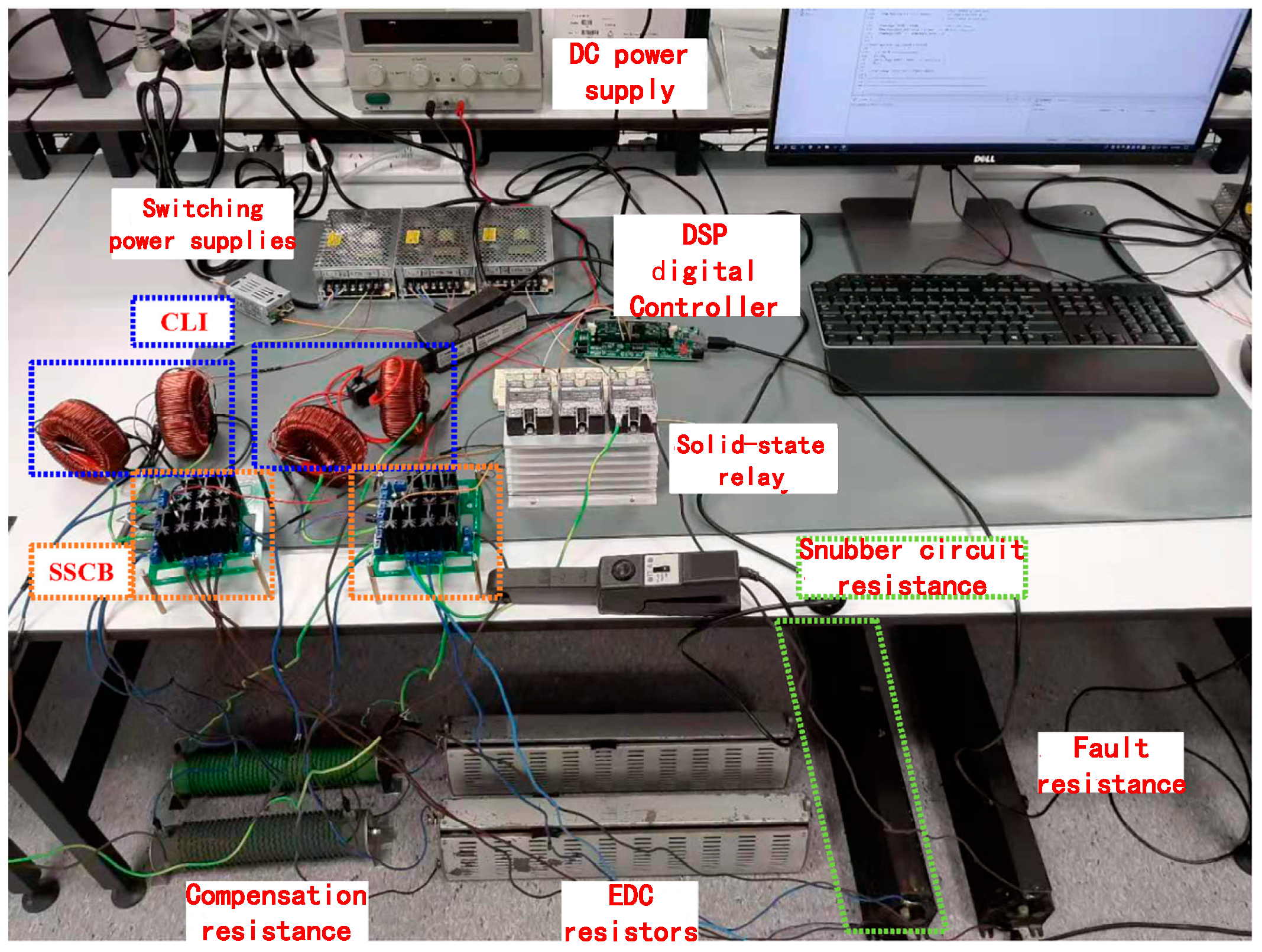
3.1. Simulation Platform Construction

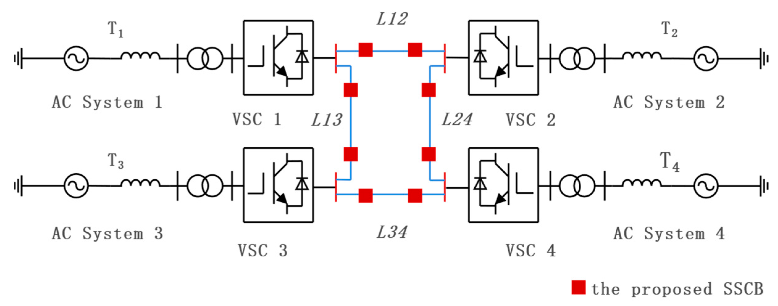
A four-terminal VSC-MTDC system was established in a SIMULINK real-time simulator, as shown in Figure 5. The main system parameters are listed in Table 1. Solid-state circuit breakers (SSCBs) were installed at the DC line terminals, and the simulation primarily demonstrated pole-to-pole (PP) faults and load variations.
The steady-state DC line current was maintained at 2.6 A. Pole-to-pole (PP) faults were generated by a DC solid-state relay (SSR). According to university laboratory safety requirements, the maximum fault current needed to be limited to less than 25 A. Nevertheless, this range was analogous to typical fault currents in low-voltage DC systems (i.e., 63 A). Furthermore, the primary objective of this study was to characterize the SSCB’s performance; thus, greater emphasis was placed on the fault current waveform profile. Building upon this work, future research will extend it to testing in industrial-scale installations.
While the detailed analysis focused on the fault current waveform profile (magnitude, di/dt, etc.) as a key indicator of SSCB performance during the initial fault interruption phase, it is crucial to acknowledge the fundamental physical significance of the subsequent switching process, particularly concerning the Transient Recovery Voltage (TRV). Following successful current interruption by the SSCB, the TRV is the voltage transient that appears across its opening contacts. This voltage stresses the newly formed gap and is critical for determining whether the interruption is ultimately successful (arc does not re-ignite) or fails.
The magnitude and wave shape of the TRV were governed by the system’s inherent parameters (inductance, capacitance, and resistance) and the magnitude of the interrupted current. Crucially, the physical implications of the TRV scale dramatically with system voltage and current levels. A TRV of 10 V across a contact gap interrupting 10 A presents negligible stress on insulation and poses minimal re-ignition risk. In stark contrast, a TRV reaching 100 kV across contacts interrupting 10 kA imposes extreme dielectric stress, demanding sophisticated contact design (e.g., larger gaps, arc chutes, and vacuum/SF6 insulation) and precise control to manage the intense electric field and prevent destructive re-strikes. Similarly, interrupting 10 kA generates vastly higher electromagnetic forces, contact erosion, and arc energy compared to interrupting 10 A, fundamentally altering the stresses on the switching device.
Therefore, while the present study utilized RTDS and focused on characterizing SSCB behavior under the constrained, low-energy conditions (25 A max fault current and the low system voltage implied by the TRV levels achievable in this setup) pertinent to the laboratory safety scale and analogous low-voltage DC applications, we explicitly recognize that scaling to industrial-level voltages (hundreds of V to kV) and fault currents (kA range) introduces orders-of-magnitude greater challenges. The TRV becomes a dominant factor requiring careful design consideration, and the physical phenomena (electromagnetic forces, arc plasma dynamics, and dielectric recovery) during the interruption and the TRV phase become significantly more intense and complex. Future work targeting industrial applications will necessitate dedicated investigations of SSCB performance under these high-stress TRV and high-current interruption conditions.

3.2. Analysis of Simulation Results

3.2.1. Fault Clearing Simulation Analysis

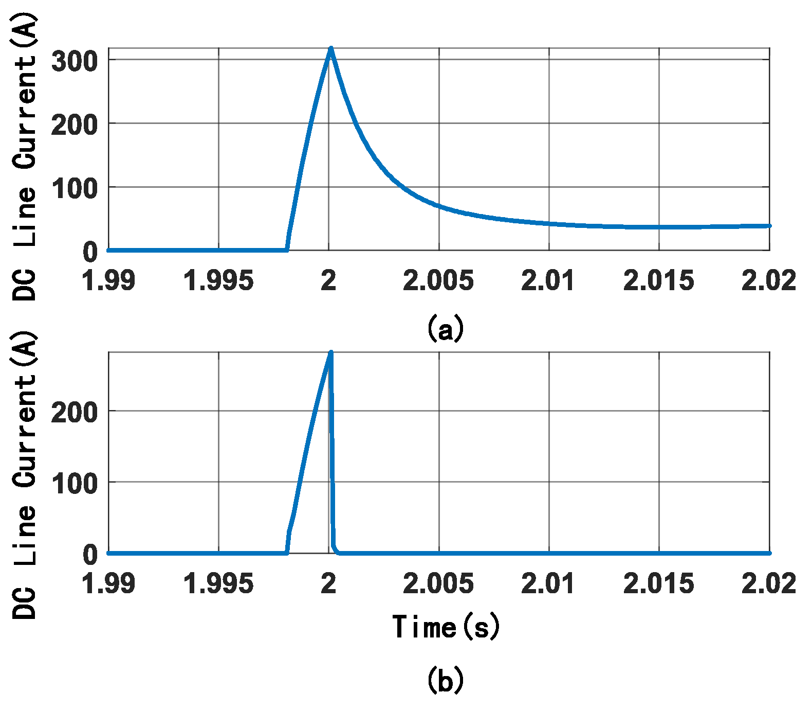
The SSCB designed in this paper was set to initiate a fault signal at 1.998 s. The current in the DC circuit path is shown in Figure 6. As can be seen in the figure, the current started to drop abruptly after a 0.02 s delay post-fault. This was because the current-limiting branch incorporated a DC bias source. The current-limiting effect was only activated when the fault current exceeded the DC bias current, causing IGBT S3 to interrupt. This action thus altered the current path, interrupting the fault current after it reached its peak.
Furthermore, as shown in Figure 6, the fault current in the mutual-inductor-based current-limiting scheme exhibited a gradual decline due to the inductance restricting abrupt current changes, resulting in an excessively long current-limiting period. In contrast, the fault current in the designed SSCB demonstrated a nearly vertical slope during its descent, significantly reducing the fault isolation time.

3.2.2. Current-Limiting Simulation Analysis

Under conditions without triggering tripping, a functional comparison of the two current-limiting methods was conducted. As shown in Figure 7, both the mutual-inductor-based current-limiting scheme and the designed SSCB current-limiting method could effectively suppress diode current disturbances and active power disturbances in VSC1, as well as reduce the peak current in the faulted line. The figure reveals no significant visual difference between the waveforms produced by the mutual-inductor-based scheme and the designed SSCB method. However, these two distinct current-limiting approaches exhibited significant differences in other functional aspects.

3.2.3. Simulation Analysis of Current-Limiting Inductor Voltages When Using Different Resistors

The voltage variation across the current-limiting inductor under different resistances is shown in Figure 8a. When a fault pulse occurred at t = 1.998 s, the voltage across the inductor instantly surged. This phenomenon occurred because the inductor current could not change abruptly while the inductor voltage could experience instantaneous changes. Within a short duration, the inductor voltage rapidly climbed to its peak. During the period from 1.998 s to 2 s, the current-limiting voltage initially rose to its peak value and then gradually declined, maintaining an overall inductor voltage below 60 V. At t = 2 s, when the IGBT tripped, the current-limiting voltage dropped rapidly. This enabled immediate isolation of the DC line, even while the current-limiting inductor continued dissipating energy for a brief period.
As indicated in the figure, when the resistance in the energy dissipation circuit (connected in parallel with the current-limiting inductor) was altered, the voltage across the current-limiting inductor changed accordingly. At t = 2 s, when the IGBT began to trip, the current was diverted from the current-limiting path to the energy dissipation circuit. Since inductor current cannot change instantaneously, the voltage across it increases with higher resistance values. The duration of this voltage is governed by the time constant (τ), where τ = L/R. For a fixed inductance, more resistance results in a shorter voltage duration. Therefore, by comprehensively considering the subsequent voltage across the IGBT, an appropriate resistance value was selected to enable rapid dissipation of the energy stored in the current-limiting inductor.

3.2.4. Simulation Analysis of IGBT Voltage Under Different Resistances

As shown in Figure 8b, the voltage variations across the IGBT under different resistances after fault occurrence demonstrated the following behavior: At the initial fault inception (t = 1.998 s), the IGBT maintained its conducting state due to its inherent high input impedance, while the fault current remained below the DC bias current. At t = 2 s, when the fault current exceeded the DC bias current, the freewheeling current through the current-limiting inductor and line inductance generated a back electromotive force (EMF) during the subsequent fault current decline. This back EMF forced the IGBT to turn off, thereby interrupting the fault current.
As observed in the figure, the voltage across the IGBT differed at resistance values of 10 Ω, 5 Ω, and 1 Ω. For IGBT voltage, lower values are preferable since excessive voltage may cause breakdown, preventing normal operation after fault recovery. Considering the voltage behavior across the current-limiting inductor under different resistances (as previously analyzed), we must ensure both rapid dissipation of energy from the current-limiting voltage and maintenance of the IGBT voltage within a safe threshold. This study adopted 5 Ω for the resistor in the energy dissipation circuit.

3.2.5. Fault Ride-Through Simulation Analysis

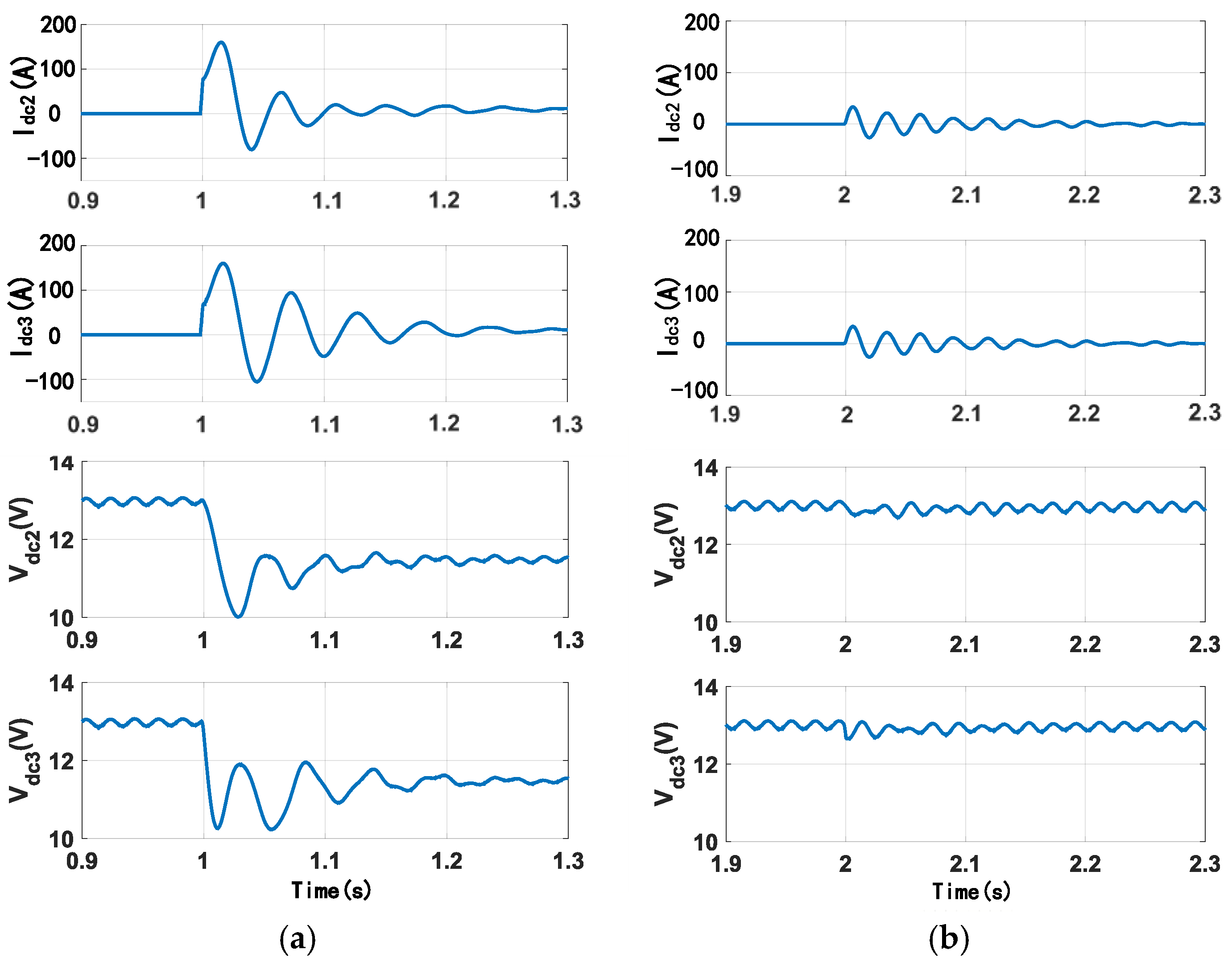
Following the trip event at t = 2 s, the system response of healthy components to the fault occurrence is illustrated in Figure 9. Here, Idc2 and Idc3 represent the DC currents of VSC2 and VSC3, respectively, while Vdc2 and Vdc3 denote the DC voltages of VSC2 and VSC3, respectively.
The DC current and voltage limits of the voltage regulator were set to 4 × IdN = 200 A and M × UdN = 11.05 kV (where M is the modulation index of the voltage regulator, taken as 0.85 in this study). As shown in Figure 9, the mutual-inductance current-limiting method could restrict the DC current of the VSC, but the VSC’s DC voltage decayed below 11.05 kV. In contrast, with the designed SSCB, after the trip event occurred, both the DC current and voltage of the VSC remained essentially stable. Therefore, by adopting the proposed SSCB scheme, the healthy portion of the flexible DC system successfully rode through the DC fault.

4. Experimental Results

4.1. Experimental Platform Construction

The experimental DC system was configured as shown in Figure 10, with the DC voltage maintained at 130 V, the DC bias current at 3 A, and the steady-state DC line current at 2.6 A. Pole-to-pole (PP) faults were generated using a DC solid-state relay (SSR). Per university laboratory safety requirements, the maximum fault current needed to be limited to below 25 A, although this value is similar to typical fault currents (63 A) in low-voltage DC systems. Due to the laboratory’s lower voltage level, this study did not select the FZ1000R33HE3 IHM-B and Infineon DZ435N36K modules but rather employed the low-voltage-rated IHW20N120R3 and RHRG30120 modules.
The main parameters of the system are listed in Table 2. In the 130 V DC experimental system, a pole-to-pole (PP) fault was initiated at t = 0.025 s, and the SSCB tripped at t = 5.025 s.

4.2. Comparison with Traditional SSCB

Figure 11 and Figure 12 compares the fault current response of a traditional SSCB with or without a current-limiting inductor in a DC line with the designed SSCB. Due to the fact that the designed SSCB can only produce a current-limiting effect when the fault current exceeds the DC bias current (3 A in this study), the fault current is interrupted after reaching its peak, preserving the inherent waveform characteristics of the fault current response.
Compared with traditional SSCBs without current-limiting inductors, the designed SSCB reduces the ratio of the maximum fault current to the rated current from 8.4 to 5.8. In addition, due to the presence of an EDC, the designed SSCB can instantly isolate DC lines (≤0.1 ms). In contrast, traditional SSCBs with or without current-limiting inductors require 0.3~0.5 milliseconds for MOVs to dissipate energy after tripping.

5. Conclusions

This paper proposes a novel SSCB topology with adaptive fault current-limiting capability specifically designed for enhancing the protection and self-healing capabilities in both low-voltage DC (LVDC, e.g., 380 V, 750 V, and 1500 V DC) and medium-voltage DC (MVDC, e.g., 10 kV, 20 kV, and 35 kV DC) distribution networks. Its ultra-fast isolation performance makes it particularly suitable for critical infrastructure requiring high power availability and minimal disruption, including the following:
1. Data center power distribution: To prevent cascading failures and maintain uninterrupted operation of sensitive IT loads.
2. Electric vehicle (EV) fast-charging stations: To ensure safety and enable rapid recovery after faults in high-power charging infrastructure.
3. Shipboard and aerospace DC microgrids: Where space, weight, and fault resilience are paramount concerns.
4. Industrial DC microgrids with sensitive processes: To minimize downtime and protect expensive equipment.
5. Renewable energy integration points (e.g., PV farms and battery storage interconnections): For reliable protection of converters and DC collection systems.
The novel SSCB topology incorporates an energy dissipation circuit (EDC) with auxiliary MOV-assisted energy dissipation and a snubber circuit. The primary innovation of this work lies in proposing a topology featuring adaptive switching functionality, enabling adaptive connection of the inductor to the main DC line. Furthermore, an auxiliary energy dissipation scheme based on an energy dissipation circuit (EDC) is introduced. In this EDC, a resistor serves as the primary element for dissipating the inductor’s stored energy, while an auxiliary MOV provides voltage clamping support. This design significantly accelerates fault isolation and reduces the energy burden, hence the capacity requirement placed on the MOV compared to traditional schemes where the MOV is solely responsible for energy absorption. Consequently, the proposed scheme achieves rapid isolation of the fault line with substantially alleviated constraints imposed by MOV capacity limitations. Compared to a traditional SSCB solution with a current limiter installed directly in the DC line, simulation and experimental results demonstrate that the proposed SSCB scheme successfully achieves adaptive commutation and realizes rapid isolation of the fault line within 0.1 ms.

Author Contributions

Conceptualization, B.W. and D.L.; Data curation, H.L. and B.P.; Formal analysis, H.X. and H.L.; Funding acquisition, F.D.; Investigation, Z.L. and B.P.; Investigation, D.L.; Project administration, F.D. and Z.L.; Resources, B.W.; Software, H.X. and H.L.; Supervision, D.L. and F.D.; Validation, B.P. and B.W.; Visualization, Z.L.; Writing—original draft, H.X.; Writing—review & editing, H.X. All authors have read and agreed to the published version of the manuscript.

Funding

Natural Science Foundation of China (52167008, 52377103) and the Natural Science Foundation of Jiangxi Province (20232BAB204064, 20242BAB25284).

Data Availability Statement

The original contributions presented in this study are included in this article, and further inquiries can be directed to the corresponding author.

Conflicts of Interest

Author Benren Pan was employed by the company State Grid Jiangxi Electric Power Co., Ltd., Electric Power Science Research Institute. The remaining authors declare that the research was conducted in the absence of any commercial or financial relationships that could be construed as a potential conflict of interest.

Abbreviations

SSCBSolid-State Circuit Breaker
HCBHybrid Circuit Breaker
MOVMetal Oxide Varistor
PTCTemperature Coefficient
EDCEnergy Dissipation Circuit
PPPole–Pole
FCLFault Current Limitation
LVDCLow-Voltage DC
MCBMechanical DC Circuit Breaker
SSFALsSolid-State Fault Current Limiters
SFCLsSuperconducting Fault Current Limiters
MVDCMedium-Voltage DC
IGBTInsulated-Gate Bipolar Transistor
PGPole–Ground
SSRSolid-State Relay

References

  1. Xu, Z.; Xue, Y.; Zhang, Z. Key technologies and prospects of large-capacity overhead line flexible DC transmission. Proc. CSEE 2014, 34, 5051–5062. [Google Scholar]
  2. Zhang, Y. Research on multi-objective network reconfiguration of active distribution network. Adv. Technol. Electr. Eng. Energy 2017, 36, 29–35. [Google Scholar]
  3. Xu, Y.; Feng, Q.; Tan, Z. Power supply restoration strategy for multi-terminal flexible interconnected distribution network considering transfer and reconfiguration coordination. Trans. China Electrotech. Soc. 2024, 39, 2696–2709. [Google Scholar]
  4. Li, Y.; Chen, X.; Li, W.; Yu, S.; Xu, S.; Wei, T.; HE, Z. Research on flexible distribution network interconnection structure and control technology based on parallel connection of smart soft open points and tie switches. Proc. CSEE 2022, 42, 4749–4760. [Google Scholar]
  5. Zhang, S.; Zou, G.; Xu, C.; Sun, W. A reclosing scheme of hybrid DC circuit breaker for MMC-HVDC systems. IEEE J. Emerg. Sel. Top. Power Electron. 2020, 9, 7126–7137. [Google Scholar] [CrossRef]
  6. Li, B.; Wang, C.; He, J. DC power supply design of adaptive current-limiting solid-state circuit breaker. Autom. Electr. Power Syst. 2020, 44, 30–37. [Google Scholar]
  7. Dai, Z.; Shi, C.; Li, Y. A novel current-limiting DC circuit breaker suitable for flexible DC distribution networks. Electr. Power Autom. Equip. 2025, 45, 41–49. [Google Scholar]
  8. Yang, S.; Lei, Q.; Peng, F.Z.; Qian, Z. A robust control scheme for grid-connected voltage-source inverters. IEEE Trans. Ind. Electron. 2010, 58, 202–212. [Google Scholar] [CrossRef]
  9. Xiang, W.; Yang, S.; Adam, G.P.; Zhang, H.; Zuo, W.; Wen, J. DC fault protection algorithms of MMC-HVDC grids: Fault analysis, methodologies, experimental validations, and future trends. IEEE Trans. Power Electron. 2021, 36, 11245–11264. [Google Scholar] [CrossRef]
  10. Li, G.; Wang, Z.; Wang, Z. Research on fault isolation technology for DC distribution network based on solid-state circuit breaker. Proc. CSEE 2021, 41, 3405–3416. [Google Scholar]
  11. Zhang, F. Design of high-voltage switchgear detection system for power systems based on real-time on-resistance monitoring. China New Technol. Prod. 2022, 8, 27–30. [Google Scholar]
  12. Mu, J.; Wang, L.; Hu, J. Design and analysis of DC solid-state circuit breaker topology. Proc. CSEE 2010, 30, 109–114. [Google Scholar]
  13. Mei, J.; Zheng, J.; Hu, M. Structure and analysis of hybrid current-limiting circuit breaker based on IGBT soft turn-off. Autom. Electr. Power Syst. 2004, 28, 59–62+75. [Google Scholar]
  14. Jaafari, A.; Mohsenzade, S.; Kazemi, R.A.A. An adaptive current commutation for hybrid DC circuit breaker. Electr. Power Syst. Res. 2025, 247, 111828. [Google Scholar] [CrossRef]
  15. Zhang, B.; Wang, Y.; Li, S.; Ma, L. A Topology of Current-limiting Hybrid DC Circuit Breaker Based on Auxiliary Capacitor Commutation. Eng. Lett. 2025, 33, 1346–1355. [Google Scholar]
  16. Liu, L.; Xue, J.; Ji, F. Analysis and design of a bidirectional forced commutation DC vacuum circuit breaker topology. Proc. CSEE 2022, 42, 8034–8041. [Google Scholar]
  17. Tong, X.; Ning, D.; Xia, W. A composite voltage balancing method for series-connected IGBTs. Trans. China Electrotech. Soc. 2012, 27, 153–158. [Google Scholar]
  18. Hassanpoor, A.; Häfner, J.; Jacobson, B. Technical assessment of load commutation switch in hybrid HVDC breaker. IEEE Trans. Power Electron. 2014, 30, 5393–5400. [Google Scholar] [CrossRef]
  19. Jayamaha, D.; Lidula, N.W.A.; Rajapakse, A.D. Protection and grounding methods in DC microgrids: Comprehensive review and analysis. Renew. Sustain. Energy Rev. 2020, 120, 109631. [Google Scholar] [CrossRef]
  20. Qi, L.; Pan, J.; Huang, X.; Feng, X. Solid-state fault current limiting for DC distribution protection. In Proceedings of the 2017 IEEE Electric Ship Technologies Symposium (ESTS), Arlington, VA, USA, 14–17 August 2017; pp. 187–191. [Google Scholar]
  21. Xu, Y.; Zhao, X.; Han, M.; Xu, L.; Zhang, G.; Liu, N.; Liu, X. A self-bypass coupled inductor DC fault current limiter. Proc. CSEE 2025. [Google Scholar] [CrossRef]
  22. Dai, Z.; Liu, S.; Li, Y. Capacitor-assisted circuit breaker suitable for medium-voltage flexible DC distribution network. Acta Energiae Solaris Sin. 2024, 45, 179–187. [Google Scholar]
  23. Li, B.; He, J. Studies on the application of R-SFCL in the VSC-based DC distribution system. IEEE Trans. Appl. Supercond. 2016, 26, 1–5. [Google Scholar] [CrossRef]
  24. Sarfi, V.; Hemmati, V.; Arabshahi, M.M. Simulation of PTC devices as fault current limiters in power systems by finite element method. In Proceedings of the 2014 ICHVE International Conference on High Voltage Engineering and Application, Poznan, Poland, 8–11 September 2014; pp. 1–4. [Google Scholar]
Figure 1. The topology of the symmetrical full-bridge SSCB.
Energies 18 03613 g001
Figure 2. Current flow under normal operating conditions.
Energies 18 03613 g002
Figure 3. Current flow in current-limiting stage.
Energies 18 03613 g003
Figure 4. Current flow in fault current-clearing stage.
Energies 18 03613 g004
Figure 5. Four-terminal VSC-MTDC system.
Energies 18 03613 g005
Figure 6. A fault isolation comparison: (a) the mutual inductor and (b) the novel SSCB.
Energies 18 03613 g006
Figure 7. A fault limitation comparison: (a) the mutual inductor and (b) the novel SSCB.
Energies 18 03613 g007
Figure 8. Variation in voltage in (a) current-limiting inductor and (b) IGBT.
Energies 18 03613 g008
Figure 9. A fault ride-through comparison: (a) the mutual inductor and (b) the novel SSCB.
Energies 18 03613 g009
Figure 10. Experimental test system.
Energies 18 03613 g010
Figure 11. Fault current limiting.
Energies 18 03613 g011
Figure 12. Fault current clearing.
Energies 18 03613 g012
Table 1. Simulation system parameters.
TerminalT1T2T3T4
AC voltage (kV)4444
AC power gridFrequency (Hz)60505060
Active power (kW)300100600200
DC voltage (kV)±6.5±6.5±6.5±6.5
DC linesDC current (A)50505050
Capacitor (µF)750750750750
Table 2. The main parameters of the experimental system.
Component TypeParameterComponent TypeParameter
AC power100 Vrms, 50 HzResistive loads46 Ω, 4 KW
DC voltage130 VSSRDD220D100
DC current2.6 AIGBTIHW20N120R3
DC capacitors2700 µFDiodeRHRG30120
R1, R32 ΩR6, R72 Ω
R2, R46 ΩL1, L210 mH
R56 ΩL3, L46 mH
Disclaimer/Publisher’s Note: The statements, opinions and data contained in all publications are solely those of the individual author(s) and contributor(s) and not of MDPI and/or the editor(s). MDPI and/or the editor(s) disclaim responsibility for any injury to people or property resulting from any ideas, methods, instructions or products referred to in the content.

