Abstract
Field-programmable gate array (FPGA)-based real-time simulation plays a crucial role in testing power–electronic dominated systems with the formation of controller hardware-in-the-loop (CHIL) or power hardware-in-the-loop (PHIL). This work describes an efficient implementation of computation time and resource usage in the FPGA-based study of a modular multilevel converter (MMC) with detailed electromagnetic transients. The proposed modeling technique can be used in continuous control mode (CCM) and discontinuous control mode (DCM) for high-switching frequency semiconductor technologies. An FPGA-based designed solver structure is also presented to take advantage of the parallel features of FPGAs to achieve an ultra-fast calculation speed. In addition, two different switch modeling techniques are discussed with a five-level MMC case study. Experimental results on the NI PXIe platform show the feasibility of the proposed implementation, and a time step of 100 nanoseconds is achieved.
1. Introduction
Modular multilevel converters (MMCs) are widely applied in power transmission and conversion in power grids and electrified transportation. However, testing MMCs with high power is a great danger due to the high voltage and current involved. In addition, the prototype is prone to be damaged without precautions. On the other hand, hardware-in-the-loop simulation (HiLs) serves as an effective form of testing and validation of the prototype by simulating the power electronic system using a digital real-time simulator (DRTS) [1]. This can minimize the developing period and reduce the danger of damaging and destroying prototypes [2]. However, the design of HiLs depends on the mathematical model of the MMC, the calculation time of which will affect the stability of the real-time system.
In a power-electronic-dominated system simulation, the choice of the time step relates to the typical application and the implementation hardware. A relatively low time step is required to maintain numerical stability for studying power systems or electrical machines. A time step ranging from 50 µs to 200 µs is necessary to consider the effect of the third or fifth harmonic in the power system [3]. This time step can provide acceptable results for electromagnetic transients up to 1 kHz. This can be implemented on a simulator using CPU/DSP as the core computational engine [4]. A power system involving multiple power electronic systems requires a time below 50 µs to perform the transient analysis of power systems.
For time steps below microseconds, FPGAs have to be involved [5]. This time step presents a detailed representation of electromagnetic transients and high frequencies inside power electronic systems. A higher-order numerical solver can achieve greater precision. The transient process of the switch devices, similar to the IGBT, can be simulated [6]. Compared with processor-based studies, the FPGA-based simulator can affect the system’s behavior by sampling the controller’s signals with an ultra-high resolution. This gives an acceptable accuracy with an interpolation method compensating for the internal switch events [7].
From this discussion, we can conclude that an FPGA simulator is essential for achieving a time step with hundreds of nanoseconds. In addition, the discrete solver and the modeling of the power switch are two main parts. In discrete solver design, paper [6] presents an FPGA-based DRTS environment for analyzing the electromagnetic transients of power systems, including multiple power electronic converters. Different subsystems are divided by utilizing the Switching-Network Partitioning (SNP) method. Using the parallel calculation of FPGAs enables sub-microsecond simulation time steps. Paper [7] utilizes the LabVIEW Platform 2021 and implements the power converters model using LabVIEW FPGAs. LabVIEW provides a single-cycle time loop structure and achieves a time step of hundreds of nanoseconds. Paper [8] presents a general implementation of the FPGA-based simulation of photovoltaic applications. After representing the system with ODEs using Xilinx system generator tools, a time step below 1 microsecond is obtained.
However, this solver is restricted by sequential calculation, and parallel solving can improve the solving speed [9,10]. Paper [11] proposes a similar approach to real-time simulation using a multi-rate structure. By modeling the power electronic system using different time resolutions, the solving is not sequential, and all subsystems can be solved simultaneously. Paper [12] proposes apredictor–corrector parallel solver for FPGA implementation. An independent solving process is obtained after separating the solving relationship between the predictor and corrector calculation. After implementing LabVIEW FPGAs, the time step is significantly reduced to 100 nanoseconds. The other decoupling method is a multi-rate simulation with a different solver [13,14]. A parallel process can be achieved by partitioning the whole system using different time steps. However, the latency among different subsystems and the synchrony of the subsystem are two potential problems.
The other key factor that affects the calculation speed is the judgment of the switches. In general, the ideal switch function model [15], the Ron/Roff model [16], and the associated discrete circuit model [17] are three commonly used models for system-level simulations with a detailed representation of the switch steady-state effect. Although the transient state of the switch can further improve the system accuracy, the model size is largely limited due to the hardware resource of FPGAs [18]. In system-level simulations, similar to the DCM condition, an iteration is required to maintain the stability of the real-time model. Paper [19,20] utilizes the iteration process to find the value when the current reaches zero. The maximum iteration times are defined to avoid overrun under the real-time constraint. On the other hand, paper [21] proposes a zero-crossing method seeking the current value when the MMC’s bridge is in the blocked mode. The zero-crossing method forces the current value to zero once the transmission from CCM to DCM is captured. This avoids the complex iteration process and can be used for CCM and DCM statutes.
This paper aims to develop a highly efficient MMC model using FPGAs. The rest of this article is organized as follows: Section 2 describes the FPGA solver design, including the ODE-solving and switch judgment processes. Section 3 presents the system model of MMCs using the ideal and Ron/Roff switch models. Section 4 offers the conclusion.
2. FPGA Solver Design
In this section, the solver of a power electronic system is illustrated. Three factors are involved. One is the discrete integration solver. The second part is the judgment of the switch status. The last is the circuit implementation on FPGAs.
2.1. ODE Solver Design
In power electronic simulations, the ordinary differential equation (ODE) form in Equation (1) can be used to describe the system behavior.
where is the input vector, is the state vector, is the derivative function, and , is the output vector. is the coefficient matrix containing the system parameters.
In general, the solving of (1) involves the integration method. One commonly used method is the Backward Euler (BE) method. In the -th time step, (1) is rewritten using BE as Equation (2) [22],
To solve x(n), two methods have been used in the literature. One is the iteration method. The other is the direct solution [23]. The error should be defined in the iteration method to end the calculation loop in each time step. The maximum iteration times are restricted so that real-time constraints can be met. One type of iteration is the improved Euler method, with the formation in Equation (3)
where is the value first calculated with the forward Euler method, and it is used to approximate the value of . Then, in the backward Euler formation, x(n) is replaced with to finish the calculation. This significantly saves the calculation time without much iteration time. The other method is the direct solution. In this method, Equation (2) is deduced from Equation (4),
Equation (3) is a direct solution to Equation (2). Since exists in Equation (4), x(n) has value with the condition that . Compared with the iteration method in Equation (2), the direct solution requires more mathematical power and calculation time to solve the inverse matrix of . So, usually, the iteration process with limited iteration time has the advantage of fast calculation. However, iteration is a sequential process, the calculation time of which can be further accelerated with a parallel process.
As shown in Figure 1, the parallel structure calculates the value at time point with a time step of . At the same time, is calculated with the value obtained from the time step of . The value of is calculated and known at the beginning of time step . Thus, the calculation of does not need to wait for the calculation of at the time step of . Since the solving of and is independent, they can be calculated at the same time. This method can be effectively used when the simulation time step is relatively small.
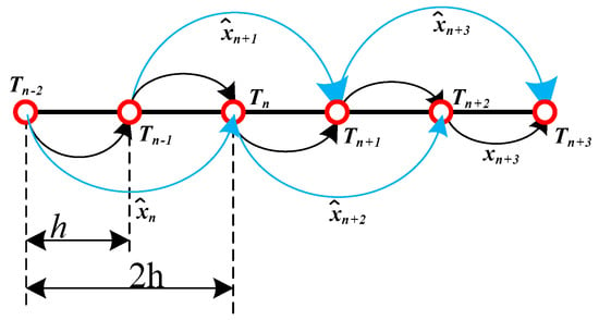
Figure 1.
The parallel solving structures.
The parallel solving process can be written as shown in Equation (5),
Compared with Equation (4), the solving process is independent. The implementation of Equation (5) will have a speed advantage.
2.2. Switch Status Update and DCM Modeling
One of the essential elements in the power electronic system is the power semiconductor device. The number of possible topologies in one power electronic system relates to the number of switches. If N is the switch’s total number, the potential power electronic system’s combination is . This time-varying feature of the power electronic system is one of the biggest challenges in modeling. For instance, if = 10, the size of the data required to store all the statuses of the circuit elements can be enormous.
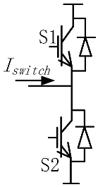
For non-controlled switches such as diode elements, its state depends on or as input for the current calculation step. In Table 1, the three basic subsystem types of switches are summarized. In the parallel calculation structure, the calculation of Iswitch has to be associated with the inductor connected to it. When the diode is in parallel with an insulated gate bipolar transistor (IGBT), its status will also be decided by the injection current as long as the drive signal is equal to zero. The switch state update comes after the value of the predictor or corrector is calculated.

Table 1.
Switch judgment.
The system modeling separates the switch’s status from the inductor or the capacitor. The circuit partitioning with the switch is shown in Figure 2, with the formation of a tow-port subsystem. In one time step, since the current flowing through the inductance or the voltage between the capacitance is constant, the connected capacitor is treated as the voltage source, and the inductance is treated as the current source. After obtaining the switch statutes from Table 1, the calculation of the unknown value [] is deduced from Equation (6).
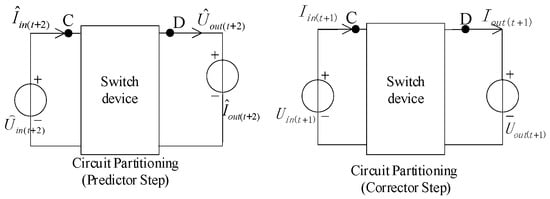
Figure 2.
Circuit partitioning with switch.
From Table 1, the value of Iswitch decides the switch statutes and acts as the guard function describing the time-varying feature in one bridge. The value of Iswitch is calculated using Equation (5). Three different derivative functions can be used to describe the time-varying topology in both DCM and CCM. A basic model is shown in Equation (7).
where is the guard function, is the derivative function of CCM, and are the derivative functions of DCM. When the power electronic system translates from CCM statues to DCM statues, the zero-crossing function has to find the zero point meeting . To reduce the calculation burden in simulation, can be approximated with a defined neighborhood . Thus, (3) can be rewritten as
Combining (8) and (5), the calculation of the corrector and are shown in Equations (9) and (10), respectively.
Once is met, the next step is to obtain the numerical value of . However, and are different. Different iteration equations will be involved, which will require more hardware resources.
For a bridge with two switches, indicates that the switch status of is or [], is the DCM indicating that the switch is . With the defined boundary , here, we define the point translating from to .
- Condition I: ;
- Condition II: .
When switch is , . Here, the value of during the DCM conditions is limited to a small value that can be neglected.
At the time point , (12) and (13) are the calculations dealing with the predictor and the corrector. The function is used to monitor whether the system is in a chattering situation. Once chattering is detected, the value and in the chattering zone will be assigned to β or −β using (16) and (17). Thus, in the next simulation step , since the sign of and are different, and the DCM will be recognized as the point crossing zero. Therefore, the following point will continue to be recognized as the DCM points in both the predictor and the corrector, but the value of and are set to −β and β, which are negligible.
2.3. FPGA Implementation Structure
Figure 3 shows the FPGA implementation structure using the proposed zero-crossing and predictor–corrector methods.
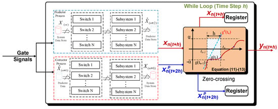
Figure 3.
Power electronic simulation with parallel calculation.
As shown in Figure 3, the system can be divided into independent subsystems by using a current source, voltage source, and two ports as a division. In each predictor calculation or corrector calculation process, the switch calculation and circuit solving have a serial connection relationship. At the time step , the solver first uses Equation (5) to calculate and after sampling the information of gate signals. is a value after two steps, and is the calculated system status. Because each variable in and is independent, and can be calculated at the same time. Compared with the forward Euler Method, the order in the parallel structure is improved to 2 [12,24].
These two values are further used to decide the system’s status in CCM or DCM using Equations (11)–(13). Furthermore, in Equations (11)–(13), the FPGA resources utilized in the zero-crossing process only involve the comparison unit, and no math calculation is used. As a result, the calculation speed is almost unaffected by the zero-crossing unit insertion.
3. System Model and Experimental Results
In this section, we show the effectiveness and the general results of the proposed method. The other case study of a five-level MMC is shown in Figure 4. Figure 4 divides the system into two parts: N1 and N2. N1 is the subsystem with inductance and capacitance. The N2 subsystem consists of the switches, which are made of a large number of power electronic submodules (SMs). The related simulation parameters are shown in Table 2.
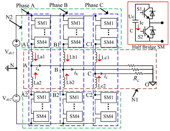
Figure 4.
Topology of a five-level MMC.

Table 2.
Simulation parameters.
3.1. Real-Time Simulation with ISF Model
The switch device of the SM in the upper bridge is shown in Figure 5a. When S1 and S2 operate in the dead zone, the switch function can be obtained with (14).
where , which represent phases A, B, and C, respectively, and j is the number of SM in the upper bridge.
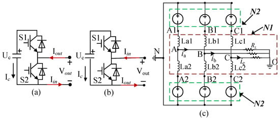
Figure 5.
The system partitioning. (a) SM is in the upper bridge; (b) SM is in the lower bridge; and (c) the N1 and N2 subsystems.
The output nodal voltage and the output current can be calculated with (15).
Thus, the current and voltage relationship in the upper bridge can be calculated with (16)
where .
With the same method, the current and voltage relationship in the lower bridge (A2, B2, C2) can be calculated with (17)–(19).
where , which represent phases A, B, and C, respectively, j is the number of SM in the upper bridge, and .
After obtaining and , the voltage relationship inside the N1 subsystem can be expressed with KVL as shown in (20),
Using (20), and can be obtained. Then, the status of the inductances can be calculated with (21):
Its discretization formulation with the predictor–corrector method can be expressed as (22),
For the capacitance in each SM, the mathematical model can be described as (23):
Its discretization formulation with the predictor–corrector method can be expressed as (24),
With an FPGA Kintex-7 XC7K410T embedded in the National Instrument (NI, Austin, TX, USA) PXIe-7975R FlexRIO PX, the model is implemented in the Express FPGA module with the structure shown in Figure 6.
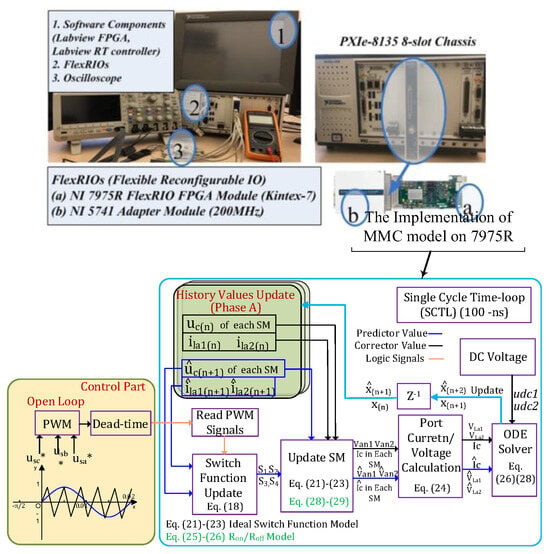
Figure 6.
Implementation on LabVIEW FPGA.
The model is implemented using the NI platform, as shown in Figure 6. The FlexRIO PXI platform contains a Kintex-7 XC7K410T FPGA. The single-cycle time loop (SCTL) allows all functions inside the loop to execute within a single tick [25,26]. The implementation of FPGAs has four sequential steps. Firstly, based on (14) and (17), the driving signals and the predictor values and determine the switch status in the correction process. Meanwhile, the driving signals and the corrector values and determine the switch status in the prediction calculation process. Secondly, we substitute the corresponding switch function into (15)–(16) and (18)–(19), so the nodal voltages and the branch currents are calculated. Then, the port voltage and current are updated using (20). Finally, (22) and (24) are computed in parallel.
After building on the FPGAs, the hardware resource utilization is shown in Figure 7, which compares the P-C method with the zero-crossing method, the P-C method without the zero-crossing method, and the forward Euler method. Although the P-C method (with/without the zero-crossing unit) has the same calculation speed (−100 ns) as the forward Euler method, the resource of the DSP48s is doubled in the P-C method. Furthermore, it can be noted that the zero-crossing process only increases by 0.5% in the Slice L.U.T.s and 0.3% in the total slices. In the meantime, the zero-crossing unit does not cause an increase in the time step or the DSP48s utilization.
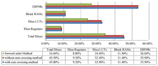
Figure 7.
The hardware resource utilization.
With a simulation step of 100 ns, the simulation results of are shown in Figure 8. Due to a long dead time of 30 µs in the PWM pulses, the current is not continuous. In the zero-crossing setup, the value of β is 1 × 10⁻⁷, and the value of α is 2 × 10⁻⁷. Figure 8a compares the Simulink results with the proposed zero-crossing method. In the Simulink results, when the current is close to zero and the MMC is in the blocked mode, the current is calculated to a value that relates to the open voltage of the IGBT device. However, the calculation of this current is a complex process. The Simulink model utilizes iteration and zero-crossing methods to seek this point. This is an offline process requiring much calculation time to finish. For a real-time simulation, the calculation burden is too heavy to seek the point crossing zero.
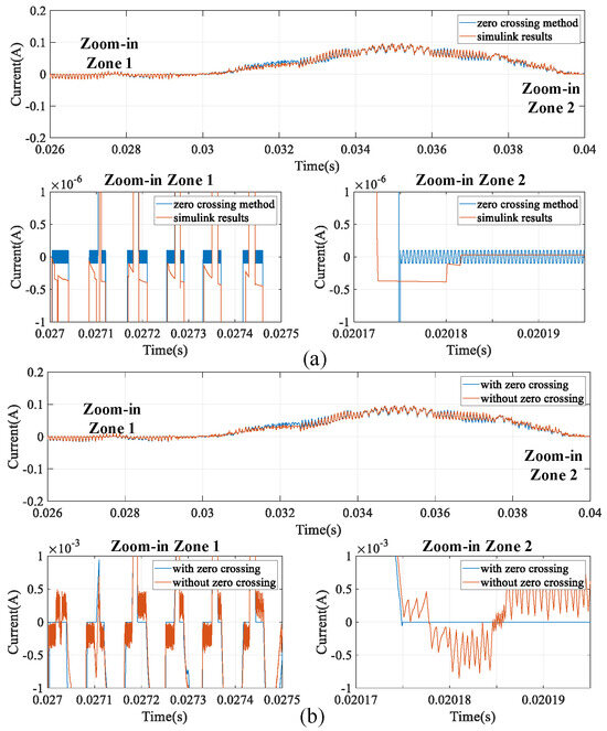
Figure 8.
Current in the ISF model: (a) comparison with the Simulink results and (b) comparison with the non-zero-crossing method.
Figure 8b shows the results of the method without using the zero-crossing method. Although the system can work normally, high oscillation exists when is close to zero, which causes a potential unstable problem in the real-time simulation. Furthermore, the high current oscillation also causes the blocked model’s virtual losses. However, in the proposed MMC model, when the bridge is in the blocked mode and the current is around zero, the proposed method can regulate the current oscillation with −1 × 10⁻⁷ and 1 × 10⁻⁷. It can also achieve a real-time simulation step of 100 nanoseconds. The proposed zero-crossing method can reduce the error and improve the accuracy when the current is around zero.
3.2. Real-Time Simulation with the Ron/Roff Model
In the Ron/Roff model, the current flowing through the switch is calculated using (25) with the value of the current .
where the status of is updated by the direction of the current . If , ; otherwise, .
As shown in Figure 9, based on Thevetin’s theorem, the SM is substituted with a voltage source in a series connection with a resistance . The value of and can be calculated with (29).
where , which represent phases A, B, and C, respectively, and j is the number of SM in the upper bridge.
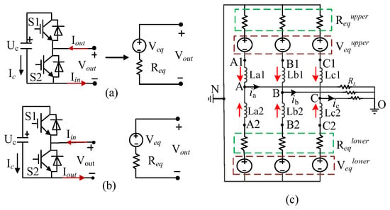
Figure 9.
The system partitioning: (a) SM is in the upper bridge; (b) SM is in the lower bridge; and (c) the N1 subsystem and N2 subsystem.
With and , the equivalent voltage and in the upper phase and the equivalent resistance and can be calculated with (27).
The current and voltage relationship in the upper and lower bridges can be calculated with (27) and (28).
After obtaining and , (25)–(27) can be further used to calculate the voltage/current status of the system. The implementation structure on the FPGA board using LabVIEW is also based on Figure 10, where the SM update unit is calculated with (28) and (29). The final FPGA resource utilization is shown in Figure 10.
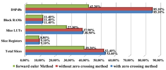
Figure 10.
The hardware resource utilization.
Compared with Figure 7 and Figure 10, the ISF and Ron/Roff models can achieve a calculation speed of 100 nanoseconds. And, because the calculation of (26) in the Ron/Roff model requires more math operations, the Ron/Roff model occupies more FPGA resources than the ISF model.
Figure 11 shows the simulation results of the current in the Ron/Roff model. In Figure 11a, the Simulink results reference the proposed zero-crossing method. The proposed method can regulate the current oscillation with −1 × 10⁻⁷ and 1 × 10⁻⁷ when the current is around zero. Compared with the P-C method without the zero-crossing method (Figure 11b), the proposed zero-crossing method increases the stability and the accuracy of the whole system simulation.
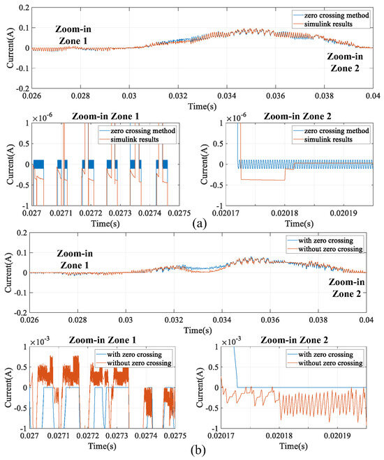
Figure 11.
Current in the Ron/Roff model: (a) comparison with the Simulink results and (b) comparison with the non-zero-crossing method.
4. Conclusions
This paper proposes an efficient real-time FPGA model of MMC to give a full representation of transient with a time step of 100 ns. Performance evaluations on different switch models (ISF and Ron/Roff models) using a five-level MMC are carried out. Compared with the traditional FPGA solver, the proposed solving structure keeps the same speed as the FE method, and the total calculation time is only 100 ns under the STCL of the LabVIEW FPGA. When the PWM has a dead-time zone, and the switch operates in the blocked mode, the proposed method can regulate the current to −1 × 10⁻⁷ and 1 × 10⁻⁷. Furthermore, the proposed method has a strong generality, which can be used in the ISF and Ron/Roff models.
The proposed solver for the power electronic system contains a parallel ODE-solving structure and the zero-crossing method. The solver can enhance the robustness by allowing the simulation of DCM and CCM with the same model. Implementing the FPGA will further reduce the simulation step under 100 ns with the detailed representation of the MMC electromagnetically transient. The ultra-fast speed advantage also allows for predicting the system behavior as fast as possible. Thus, it can be further used in the digital twin setup [27] and the model predictive control.
Author Contributions
Conceptualization, methodology, and writing—original draft preparation, W.G.; software, validation, formal analysis, investigation, resources, and data curation, C.L.; supervision, M.W.; project administration and funding acquisition, X.Z. All authors have read and agreed to the published version of the manuscript.
Funding
This work was supported by the Key Laboratory of HVDC, Electric Power Research Institute China Southern Grid, Grant agreement No: SEPRI-K223001.
Data Availability Statement
The data presented in this study are available on request from the corresponding author. The data are not publicly available due to unpublished work in process.
Conflicts of Interest
The authors declare no conflicts of interest.
References
- Bai, H.; Liu, C.; Breaz, E.; Al-Haddad, K.; Gao, F. A review on the device-level real-time simulation of power electronic converters: Motivations for improving performance. IEEE Ind. Electron. Mag. 2020, 15, 12–27. [Google Scholar] [CrossRef]
- Bélanger, J.; Venne, P.; Paquin, J.-N. The what, where and why of real-time simulation. Planet Rt 2010, 1, 25–29. [Google Scholar]
- Dufour, C.; Ould Bachir, T.; Grégoire, L.A.; Bélanger, J. Real-time simulation of power electronic systems and devices. In Dynamics and Control of Switched Electronic Systems: Advanced Perspectives for Modeling, Simulation and Control of Power Converters; Springer: London, UK, 2012; pp. 451–487. [Google Scholar]
- Kumar, P.; Kashyap, Y.; Castelino, R.V.; Karthikeyan, A.; Sharma, K.M.; Karmakar, D.; Kosmopoulos, P. Laboratory-Scale Airborne Wind Energy Conversion Emulator Using OPAL-RT Real-Time Simulator. Energies 2023, 16, 6804. [Google Scholar] [CrossRef]
- Castellini, L.; Gallorini, F.; Alessandri, G.; Alves, E.F.; Montoya, D.; Mudigonda, B.; Tedeschi, E. Comparison of Offline, Real-Time Models and Hardware-in-the-Loop Test Results of a Power Take-Off for Wave Energy Applications. J. Mar. Sci. Eng. 2022, 10, 1744. [Google Scholar] [CrossRef]
- Maguire, T.; Warkentin, B.; Chen, Y.; Hasler, J. Efficient techniques for real time simulation of MMC systems. In Proceedings of the International Conference on Power Systems Transients (IPST), Vancouver, BC, Canada, 18–20 July 2013; pp. 1–7. [Google Scholar]
- Ashourloo, M.; Mirzahosseini, R.; Iravani, R. Enhanced model and real-time simulation architecture for modular multilevel converter. IEEE Trans. Power Deliv. 2017, 33, 466–476. [Google Scholar] [CrossRef]
- Mirzahosseini, R.; Iravani, R. Small time-step FPGA-based real-time simulation of power systems including multiple converters. IEEE Trans. Power Deliv. 2019, 34, 2089–2099. [Google Scholar] [CrossRef]
- Estrada, L.; Vázquez, N.; Vaquero, J.; de Castro, Á.; Arau, J. Real-Time Hardware in the Loop Simulation Methodology for Power Converters Using LabVIEW FPGA. Energies 2020, 13, 373. [Google Scholar] [CrossRef]
- Koutroulis, E.; Kalaitzakis, K.; Tzitzilonis, V. Development of an FPGA-based system for real-time simulation of photovoltaic modules. Microelectron. J. 2009, 40, 1094–1102. [Google Scholar] [CrossRef]
- Benigni, A.; Monti, A. A parallel approach to real-time simulation of power electronics systems. IEEE Trans. Power Electron. 2014, 30, 5192–5206. [Google Scholar] [CrossRef]
- Liu, C.; Ma, R.; Bai, H.; Gechter, F.; Gao, F. A new approach for FPGA-based real-time simulation of power electronic system with no simulation latency in subsystem partitioning. Int. J. Electr. Power Energy Syst. 2018, 99, 650–658. [Google Scholar] [CrossRef]
- Milton, M.; Benigni, A. Latency insertion method based real-time simulation of power electronic systems. IEEE Trans. Power Electron. 2017, 33, 7166–7177. [Google Scholar] [CrossRef]
- Yang, G.; Li, Y.; Hao, Z.; Chen, Z.; He, P.; Zhang, J. Multi-Rate Parallel Real-Time Simulation Method for Doubly Fed Wind Power Systems Based on FPGA–CPU. Machines 2022, 10, 1073. [Google Scholar] [CrossRef]
- Ali, S.; Badar, J.; Akhter, F.; Bukhari, S.S.H.; Ro, J.-S. Real-Time Controller Design Test Bench for High-Voltage Direct Current Modular Multilevel Converters. Appl. Sci. 2020, 10, 6004. [Google Scholar] [CrossRef]
- Sang, Z.; Li, S.; Huang, Y.; Gao, X.; Qiao, R. Indirect Matrix Converter Hardware-in-the-Loop Semi-Physical Simulation Based on Latency-Free Decoupling. Electronics 2023, 12, 4802. [Google Scholar] [CrossRef]
- Alsarayreh, S.; Sütő, Z. Optimal Selection of Switch Model Parameters for ADC-Based Power Converters. Energies 2024, 17, 56. [Google Scholar] [CrossRef]
- Bai, H.; Luo, H.; Liu, C.; Paire, D.; Gao, F. A Device-Level Transient Modeling Approach for the FPGA-Based Real-Time Simulation of Power Converters. IEEE Trans. Power Electron. 2020, 35, 1282–1292. [Google Scholar] [CrossRef]
- Matar, M.; Iravani, R. Massively parallel implementation of AC machine models for FPGA-based real-time simulation of electromagnetic transients. IEEE Trans. Power Deliv. 2010, 26, 830–840. [Google Scholar] [CrossRef]
- Saad, H.; Dufour, C.; Mahseredjian, J.; Dennetière, S.; Nguefeu, S. Real time simulation of MMCs using the state-space nodal approach. In Proceedings of the IPST, Vancouver, BC, Canada, 18–20 July 2013; pp. 18–20. [Google Scholar]
- Matar, M.; Iravani, R. FPGA implementation of the power electronic converter model for real-time simulation of electromagnetic transients. IEEE Trans. Power Deliv. 2009, 25, 852–860. [Google Scholar] [CrossRef]
- Soomro, J.B.B.; Akhtar, F.; Hussain, R.; Ansari, J.A.; Munir, H.M. A detailed review of MMC circuit topologies and modelling issues. Int. Trans. Electr. Energy Syst. 2022, 2022, 8734010. [Google Scholar]
- Dufour, C.; Jalili-Marandi, V.; Bélanger, J.; Snider, L. Power system simulation algorithms for parallel computer architectures. In Proceedings of the 2012 IEEE Power and Energy Society General Meeting, San Diego, CA, USA, 22–26 July 2012; pp. 1–6. [Google Scholar]
- Li, Z.; Xu, J.; Wang, K.; Li, G.; Wu, P. A Discrete Small-Step Synthesis Real-Time Simulation Method for Power Converters. IEEE Trans. Ind. Electron. 2022, 69, 3667–3676. [Google Scholar] [CrossRef]
- Tormo, D.; Vidal-Albalate, R.; Idkhajine, L.; Monmasson, E.; Blasco-Gimenez, R. Embedded Real-Time Simulator for Sensorless Control of Modular Multi-Level Converters. Electronics 2022, 11, 719. [Google Scholar] [CrossRef]
- Single-Cycle Timed Loop FAQ for the LabVIEW FPGA Module. Available online: https://knowledge.ni.com/KnowledgeArticleDetails?id=kA00Z000000P8sWSAS (accessed on 6 November 2023).
- Dong, X.; Huang, J.; Luo, N.; Hu, W.; Lei, Z. Design and Implementation of Digital Twin Diesel Generator Systems. Energies 2023, 16, 6422. [Google Scholar] [CrossRef]
Disclaimer/Publisher’s Note: The statements, opinions and data contained in all publications are solely those of the individual author(s) and contributor(s) and not of MDPI and/or the editor(s). MDPI and/or the editor(s) disclaim responsibility for any injury to people or property resulting from any ideas, methods, instructions or products referred to in the content. |
© 2024 by the authors. Licensee MDPI, Basel, Switzerland. This article is an open access article distributed under the terms and conditions of the Creative Commons Attribution (CC BY) license (https://creativecommons.org/licenses/by/4.0/).


