1. Introduction
A key concept in power electronics is the use of an input or electro-magnetic interference (EMI) filter. In order to reduce the high-frequency noises of the power switch in any kind of power converter, a filter has to be used with the connection of the power converter to the source. The source can be direct current or alternating current. The filter requirement is not just for the input side, but for the output side of the converter between loads as well. There are two main kinds of filter: active and passive. The application of an active filter is more complex than that of a passive filter. Therefore, the implementation of a passive filter does not involve much complexity. In addition, there are a wide variety of passive filters in use with the power converter. One of the most advanced filter types is LCL-type filters. However, the use of the LCL filter, particularly the LCL trap filter with the PFC converter type, is not presented in the literature. In addition, the need for galvanic isolation in the converter is gaining attention especially for battery charging application circuits. This isolation can be achieved by a high-frequency transformer or coupled inductance. A promising topology is the isolated Ćuk converter. Due to the presence of an inductor at both the input and output sides of the converter, the filter requirements are lower. Therefore, in the present paper, the isolated Ćuk converter has been selected as a converter.
A review of the relevant studies in the literature on the topic revealed the following. Ref. [
1] introduces isolated Ćuk converter topology. The fundamental design of the converter is given in [
2]. The converter is proposed as an LED driver in [
3]. Ref. [
4] gives a detailed modeling strategy for large- and small-signal models for DC–DC converters. Large signal average modeling is proposed using a neural network in [
5]. Ref. [
6] proposes a graph representation to model the converter for CCM and DCM operation for using machine learning. A reduced order method to analyze the DCM buck converter is presented in [
7]. Ref. [
8] presents a new modeling strategy called the sigmoid function for power converters. Ref. [
9] realizes the small-signal modeling of a two-phase boost converter having a coupled inductor for DCM. Modeling of the isolated Ćuk converter is given for DCM mode operation in [
10,
11]. Ref. [
12] presents the small-signal modeling of an interleaved boost converter. Modeling of a fractional Zeta converter is derived in [
13]. Ref. [
14] describes the modeling of a boost converter with different software packages. The design and optimization of an LCL trap filter are given in [
15]. Ref. [
16] uses an LCL trap filter with an isolated Ćuk converter for DC source connection. The filter is used for the inverters as in [
17]. Ref. [
18] presents an annealing simplex method to select the inductance value in an LCL filter. Ref. [
19] uses an LCL trap filter for two level converters with grid connection. The design for an LCL trap filter for AC–DC converters by using SiC MOSFET through simulations is shown in [
20]. In order to reduce current harmonics under weak grid conditions of the converter, different trap filter structures are presented in [
21]. Ref. [
22] presents a new asymmetric LCL filter having an LC trap structure for grid-tied three-phase inverter applications.
Herein, the modeling and analysis of the LCL trap filter are carried out. Moreover, the filter effect on the isolated Ćuk converter using SiC MOSFET is investigated by a linear control methodology. The converter is operated in DCM with 42 kHz for 50 W power using linear and nonlinear loads with the LCL trap and LC filters. Furthermore, large-signal and small-signal models of the converter are derived and compared to examine the requirements of the small-signal analysis. Moreover, LTspice simulation is carried out using SiC MOSFET to compare results obtained by the applications. In addition, the results of LCL trap filter application and simulation are compared with the LC filter results and the standard. Further, parametric variation in the filter components is investigated. In conclusion, the LCL trap filter with the converter provides a 0.998 PF and 4.83% THD. These results are better than those of the LC filter and after comparison they meet the standards.
The structure of the paper is as follows. In
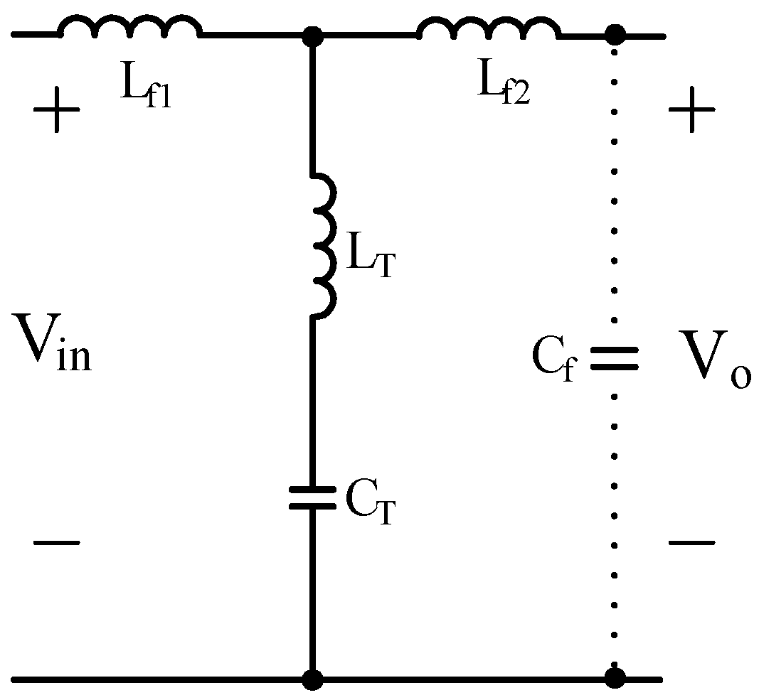
Section 2, the LCL trap filter is introduced, its design methodology is given, and its transfer function is derived. In
Section 3, the PFC isolated Ćuk converter is described, its design equations are given, and large- and small-signal models are derived with and without integrating the input filter. In
Section 4, an open-loop LTspice simulation using L and LCL trap filters is given and closed-loop control application and measurements and comparison are presented. In
Section 5, the findings are discussed and, in
Section 6, the conclusion is given.
3. PFC Isolated Ćuk Converter
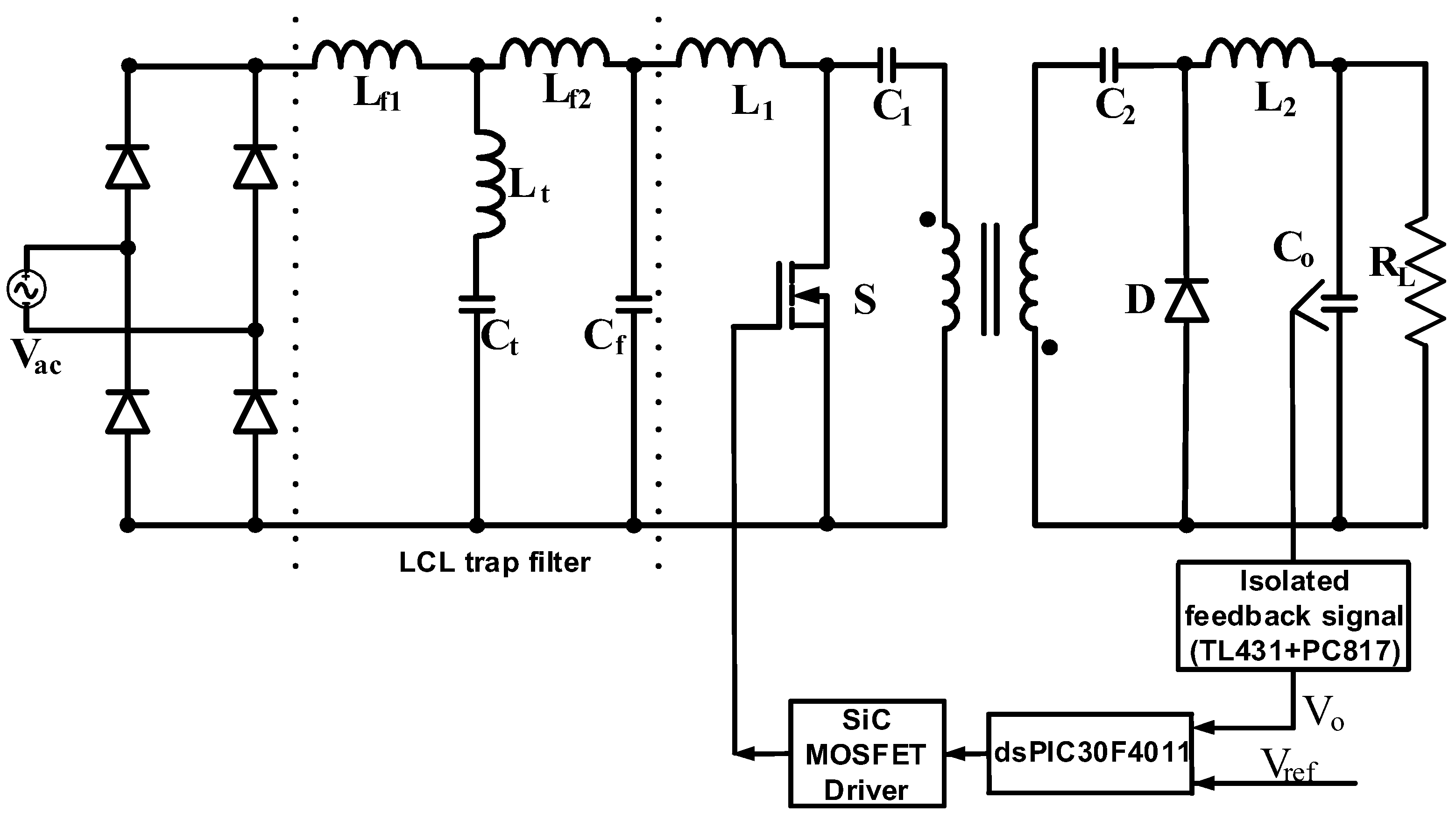
The structure of the converter with the filter is given in
Figure 3. It is seen that the converter has a transformer and two inductors and capacitors and it is connected to the grid via a diode bridge and filter. The transformer is a high-frequency transformer and provides galvanic isolation.
Converter parameters can be selected using (6)–(11) as in [
2,
10,
16]. In the equations, d is the duty cycle, n is the turns ratio, V
in is the input voltage, V
o is the output voltage, L
1 and L
2 are the inductances, C
1 and C
2 are the intermediate capacitors, C
o is the output capacitor, and R
L is the load.
A mathematical model of the converter can be derived using the Kirchhoff voltage and current laws regarding switch on and off conditions. Because of the DCM operation, the converter has three different equivalent circuits as in [
10]. The equivalent circuits are given in
Figure 4 as in [
10]. While deriving the model of the converter, it is assumed that the high-frequency transformer has ideal characteristics. Moreover, passive components are regarded as ideal, and the voltage drop in the switch is neglected.
In the modeling strategy, time ratios of each interval regarding the input side inductor current are shown in
Figure 5. It is seen that there are three different operation durations; these durations are identified as d duty cycle, δ, and 1-d-δ, matching the equivalent circuit in
Figure 4 as in [
24].
Regarding
Figure 5, the model for DCM of the converter can be derived using (12) as in [
10,
24].
After applying (12) to each equivalent circuit, a mathematical model in state-space form is obtained in (13) as in [
10].
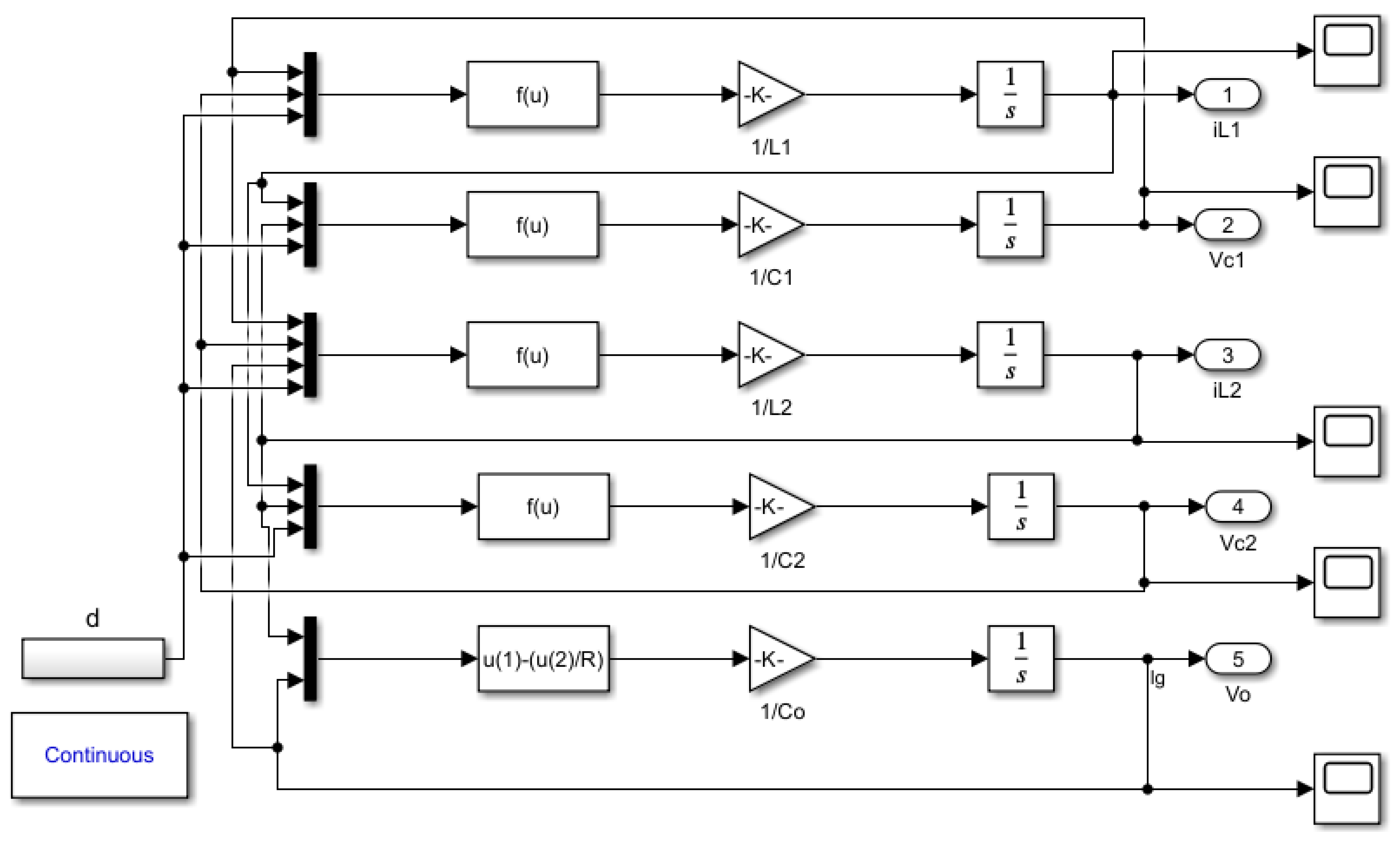
The model given in (13) is built in Simulink 9.1 in
Figure 6; this model can be called a large-signal model.
Due to the power switch, the model in (13) has nonlinear characteristics. To achieve linearization, a small-signal approach can be used. By using (14) as in [
10,
25], a control to output a small-signal transfer function can be derived in (15), as in [
10,
25]. While deriving the transfer function, steady-state values of the i
L1, i
L2, V
C1, and V
C2 parameters should be replaced regarding V
in. In the equation, k = δ/d [
10].
By using the values given' in
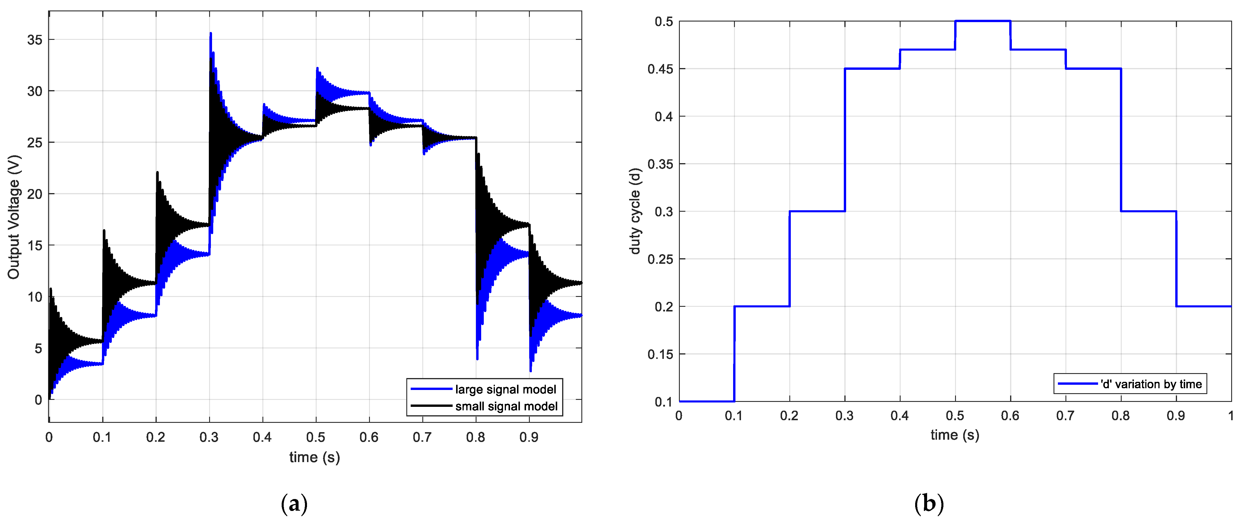
Table 1 except snubber values that are neglected in model, the step responses of the model in (13) and (15) can be drawn with different ’d’ values in
Figure 7a without considering the filter effect. The figure shows the output voltage of the converter by comparing large- and small-signal models. ‘d’ in both models is changed as in
Figure 7b.
It can be seen in
Figure 7 that each model is stable and their time responses are similar to each other and settle to some output voltage level. However, there is a steady-state error between the two models that becomes smaller close to the operating point.
Step responses in terms of d variation are repeated using an LCL trap filter with large- and small-signal models, and the comparison is given in
Figure 8. While drawing the figure, the transfer function of the trap filter in (5) is cascaded with the large-signal model in (13) and the small-signal model in (15). It is seen in the figure that the large- and small-signal models including the filter have similar characteristics but there is a steady-state error between the two models that becomes smaller close to the operating point as seen in
Figure 8. The variation in d is the same as in
Figure 7b).
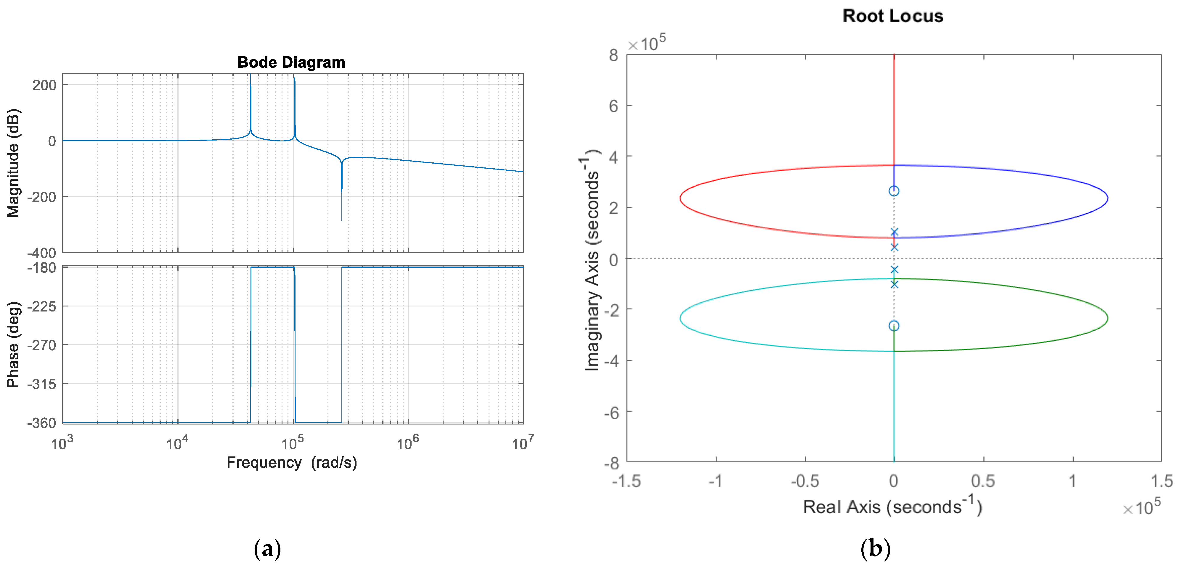
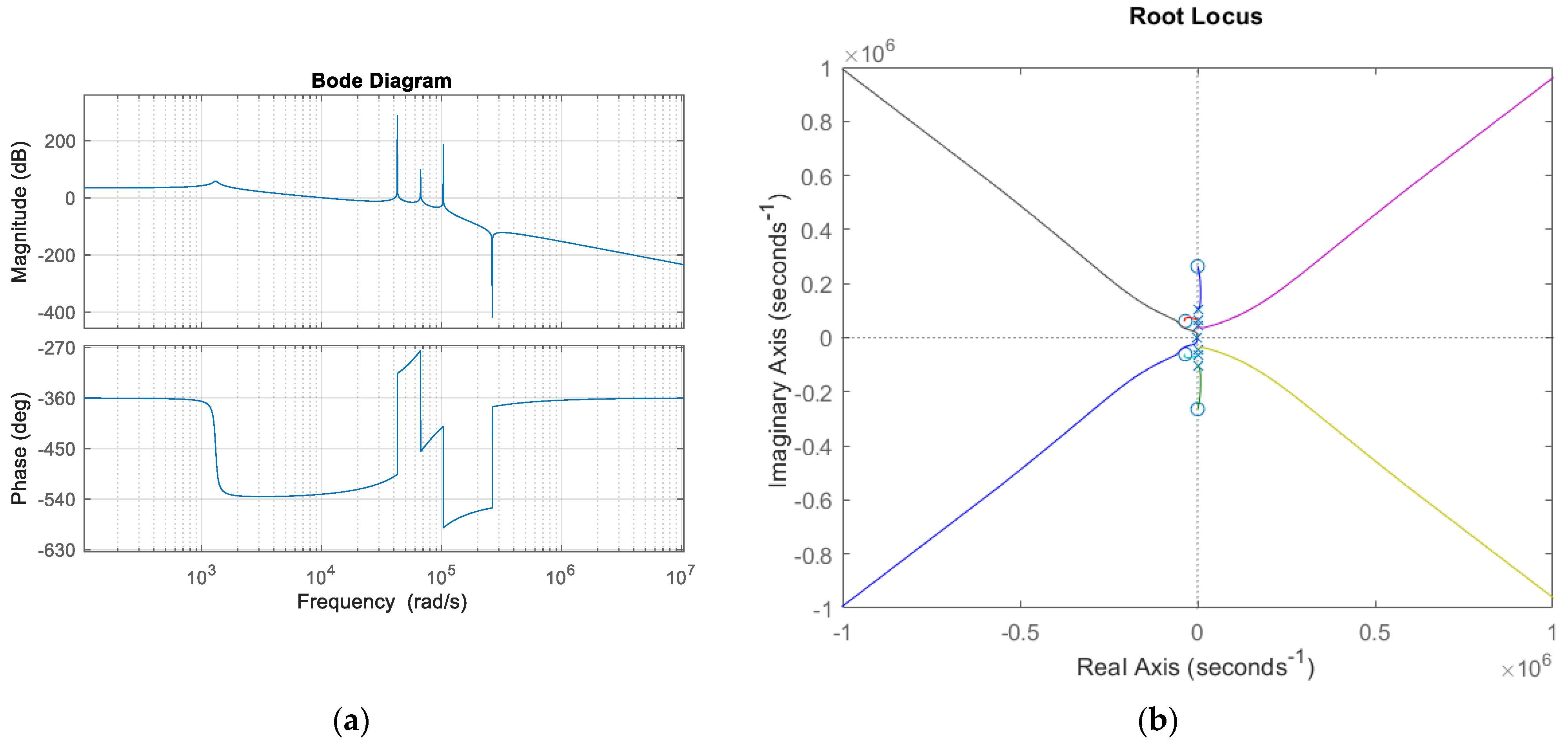
Bode and root locus graphs of the overall transfer function of the system consisting of the converter and filter are shown in
Figure 9.
4. Applications
In this section, firstly, LTspice open-loop simulations for LC and LCL trap filters are conducted and measurements including the PF, THD, and output voltage are obtained. Then, the application results using the LCL trap filter are given. The application is realized by a PI controller using isolated voltage measurement. After that, the results are presented and compared. In addition, a power diode snubber is not considered in the simulations except for in the ideal case of the simulation.
The PFC isolated Ćuk converter application using the LCL trap and LC filters is conducted by laboratory set up and the LTspice simulation using the same SiC MOSFET in the application. For applications, SiC MOSFET and dsPIC30F4011 are used as shown in
Figure 10. The converter is built for up to 50 W with a 42 kHz switching frequency. The measurement equipment is listed in
Table 2. The values of the components used in the application are given in
Table 1. Both linear and nonlinear loads are considered for both the simulation and applications. The linear load is a resistor with the value of 12.5 Ω. For the nonlinear load, six parallel 7815 voltage regulators are used. Each voltage regulator feeds a 47 Ω resistive load.
Firstly, the LTspice simulation of the system with an LC filter is conducted as shown in
Figure 11 with SiC MOSFET used in the application. By means of the simulation, the output voltage, input sinusoidal voltage, and current are given.
It can be seen in
Figure 12 that the input current is sinusoidal, the PF is 0.996 (0.995), and output voltage is 23.7 V.
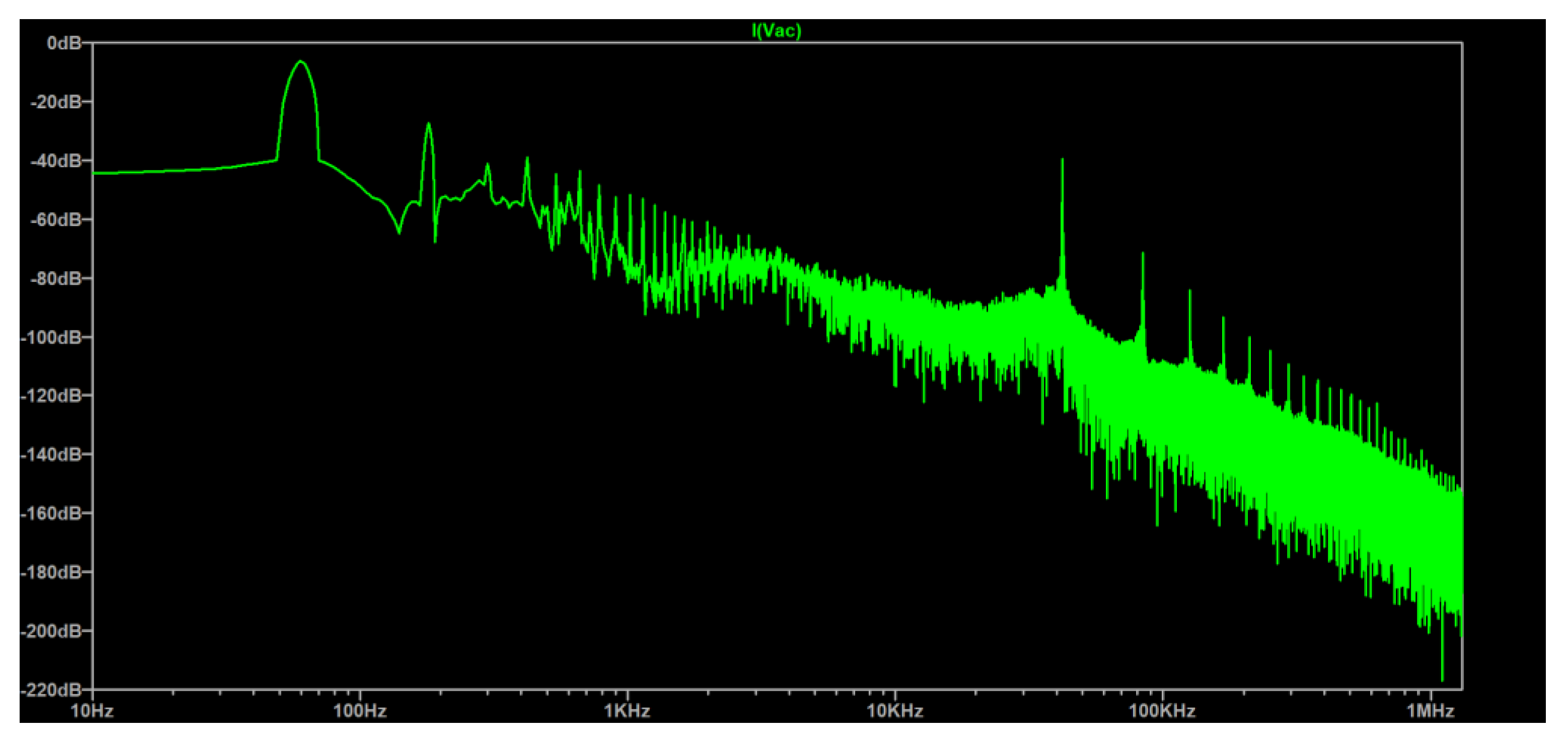
The frequency spectrum of the input current is given in
Figure 13, and the THD is measured as 8.41 (9.16)%.
The LTspice simulation of the system using an LCL trap filter with SiC MOSFET used in the application is conducted as given in
Figure 14. The output voltage and input current and voltage are measured as well.
In
Figure 15, the output voltage and input current and voltage are shown. It is seen that the output voltage is 24.7 V. Sinusoidal input current and voltage are obtained with a 0.997 PF.
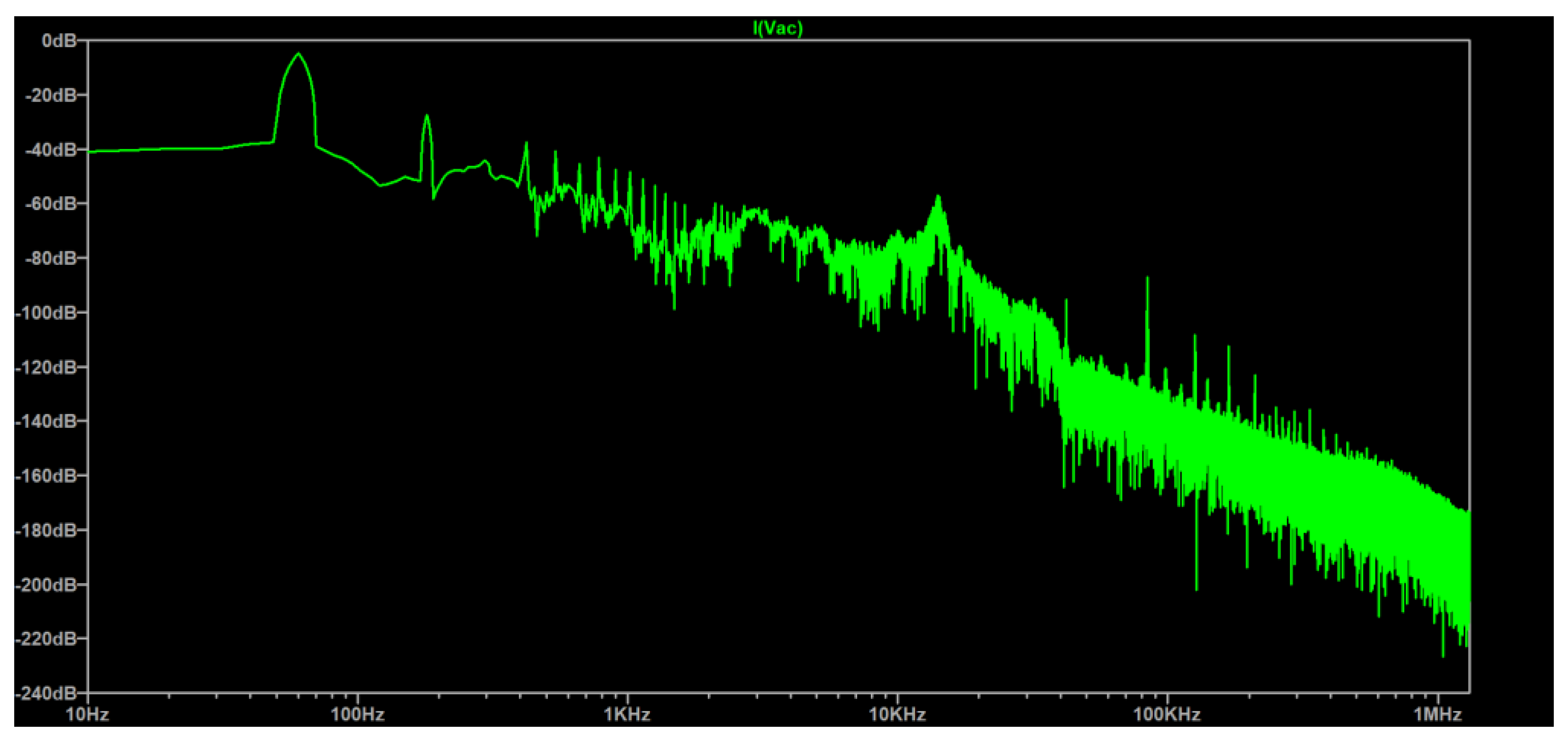
The frequency spectrum of the input current is given in
Figure 16, and the THD is measured as 8.14 (8.41)%.
In the simulations in
Figure 11,
Figure 12,
Figure 13 and
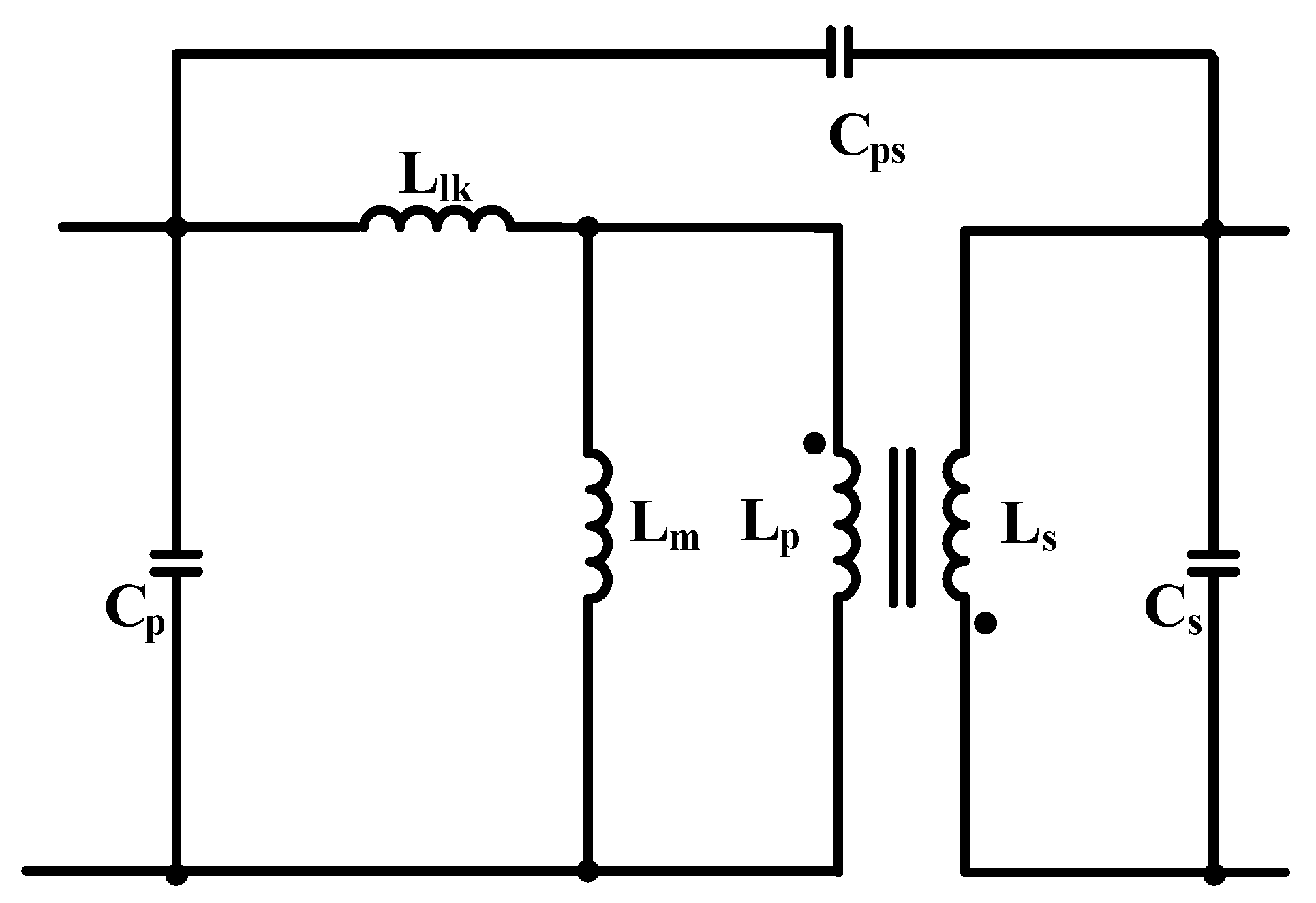
Figure 14, the transformer is regarded as ideal and load as resistive. In addition, simulations are repeated with a nonideal transformer and nonlinear loads. The values of the transformer are listed in
Table 3, and they are calculated using (16)–(20) as in [
26,
27,
28]. However, the parasitic capacitances C
p, C
s, and C
ps are the estimated values as in [
29]. Moreover, as a nonlinear load, three parallel voltage regulators feeding resistive load are connected to the output of the PFC converter. In the equations, M is the mutual inductance, k
c is the coupling coefficient, N
1 is the primary turns number, N
2 is the secondary turns number, i
1 is the primary current, L
lk is the primary leakage inductance, L
m is magnetizing inductance, and L
p and L
s are the inductances of primary and secondary, respectively. R
o is the reluctance, l
c is the effective magnetic path, μ is the permeability, and A
c is the cross-sectional area of the core. An ETD34/11/17 core with N87 material is used for the transformer.
Using the values for the transformer given in
Table 3, simulations are repeated with the model in
Figure 17. Then, all the simulation results and application results are compared in
Table 4.
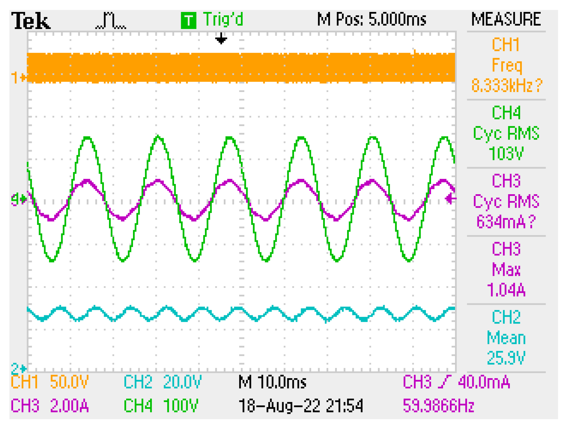
The implementation results using the LCL trap filter with linear load are for output voltage and input voltage and current in
Figure 18. The PF is measured as 1.
Figure 18 shows the PWM signal, input voltage and current, and output voltage.
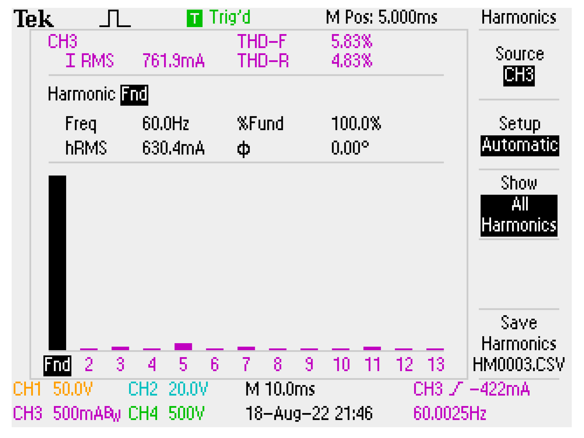
The THD of the input current is measured as 4.83% and given in
Figure 19. As the voltage THD is so low, close to 0, it is not given here.
The PF was measured with the cosθ meter as 1 without considering the grid current THD. The PF is obtained as 0.998, as in (21), after considering the grid current THD.
In addition, applications are conducted using a nonlinear load as shown in
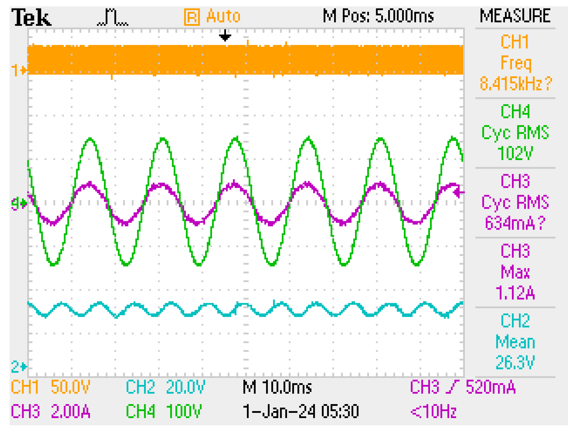
Figure 10b. The nonlinear load consists of linear regulators that have six parallel connected 7815 linear regulators and each of them is feeding a 47 Ω load. The application results using a nonlinear load are given for the LCL trap filter in
Figure 20 and
Figure 21. The PF is measured as 1. The PWM signal, input voltage and current, and output voltage are given in
Figure 20. The output voltage is obtained as 26.3 V.
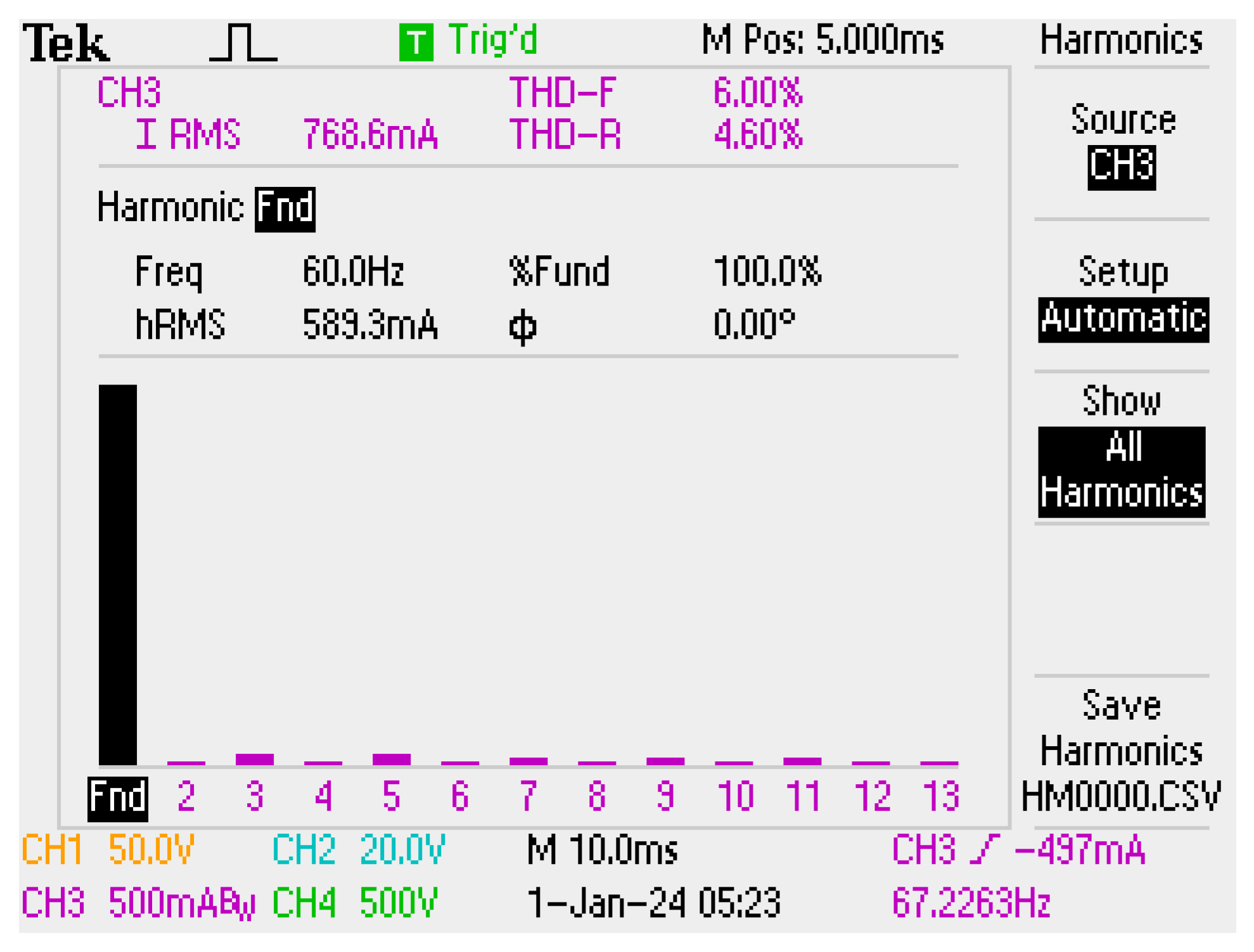
The THD of the input current of the LCL trap-filtered converter while feeding a nonlinear load is measured as 4.60% and given in
Figure 21.
The LC-filtered converter was also tested using a nonlinear load and the resulting waveforms are given in
Figure 22 and
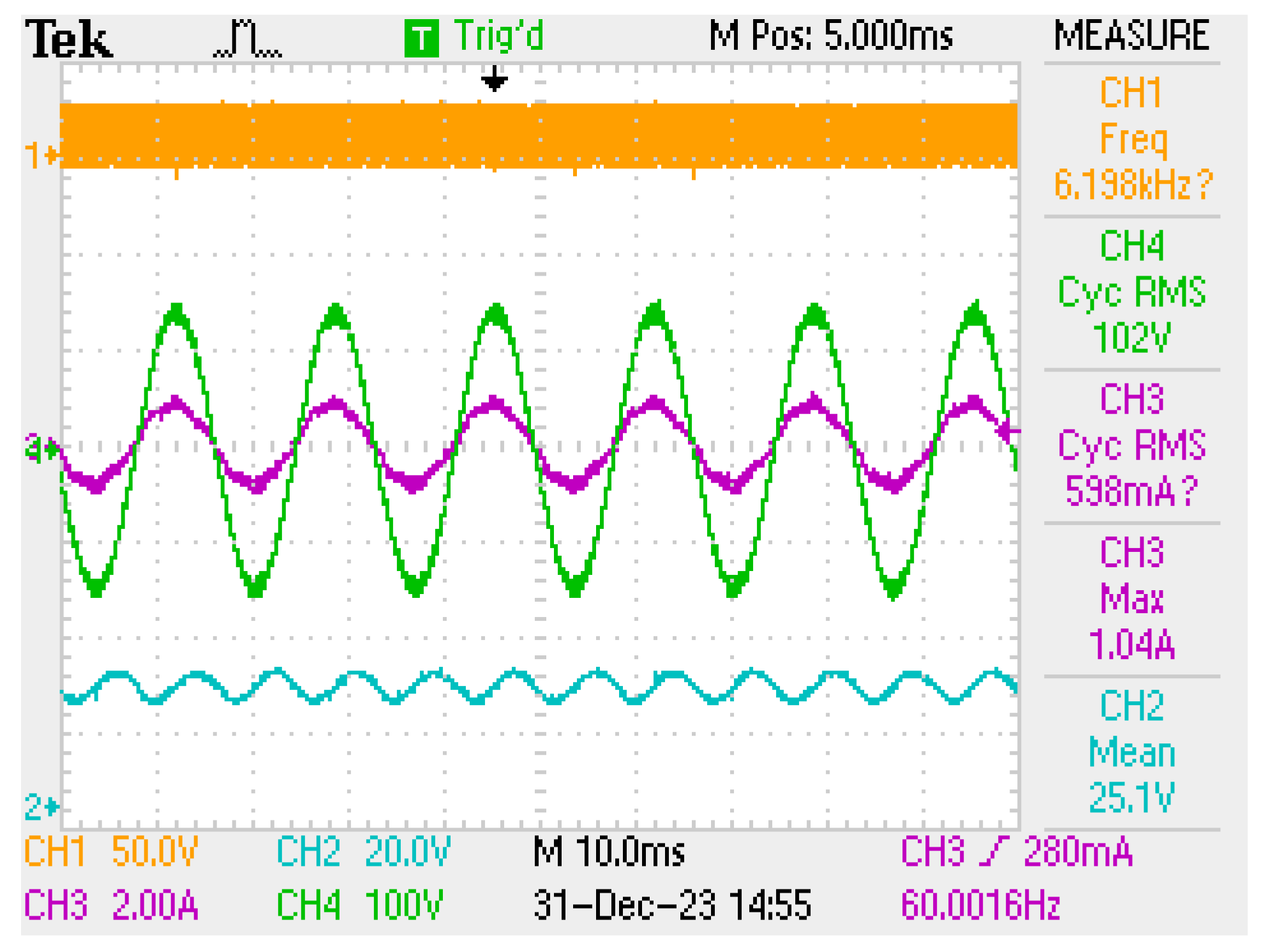
Figure 23. In
Figure 22, PWM signal, input voltage and current, and output voltage are given. The PF is measured as 0.995. It is seen that the output voltage is obtained as 25.1 V, though it has the same d of the LCL trap filter with a nonlinear load.
The THD of the input current of the LC-filtered converter while feeding a nonlinear load is measured as 6.91% and given in
Figure 23.
In
Table 4, simulation results and application results are compared regarding the load type and transformer model used as in the ideal case, with just leakage inductance and with capacitances.
To implement closed-loop control, the output voltage as a feedback signal is measured by an isolated measurement circuit as shown in
Figure 24. The isolated measurement circuit consists of a PC817 optocoupler and TL431 programmable reference IC. The circuit is shown in
Figure 10b with the feedback caption. The feedback circuit reduces the cost of isolated voltage measurement compared to the sensors available commercially but the feedback voltage does not have linear characteristics.
To control the output voltage, a PI controller is used. This controller can be designed using the root locus graph with the transfer function given in (22) as in [
30].
The PI transfer function in (22) should be cascaded with the transfer function of the whole system including the LCL trap filter and the converter. To minimize the steady-state error, the K
p/K
i ratio should be chosen close to 0 as in [
30]. After choosing the ratio as 0.001, the overall transfer function is obtained in (23).
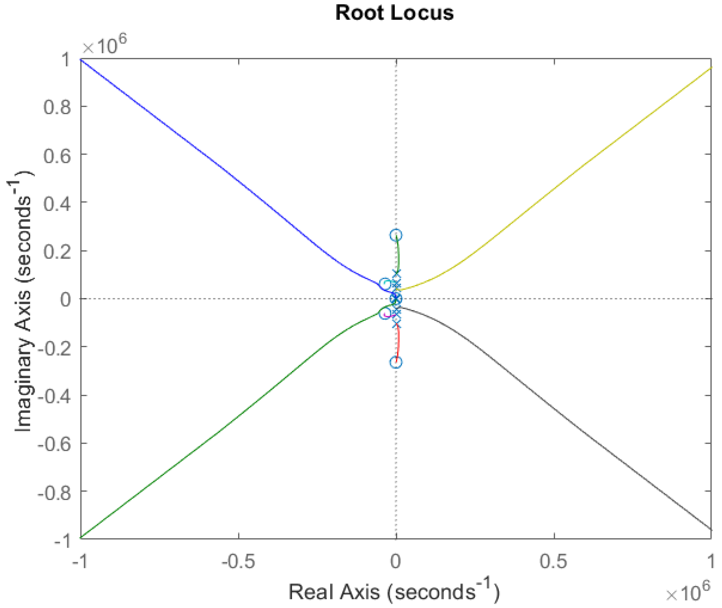
By using (23), a root locus graph can be drawn as in
Figure 25. The characteristics of the graph seem similar to those in
Figure 9b, but it can clearly be seen that a zero is added close to the origin. According to
Figure 9b, if the gain is higher than 0.0076, the system becomes unstable, so the maximum K
p should be lower than 0.0076. After choosing K
p as 0.001, K
i is obtained as 10
−6. For the LC filter, maximum controller gain is obtained as 3.09 × 10
−4 in [
10].
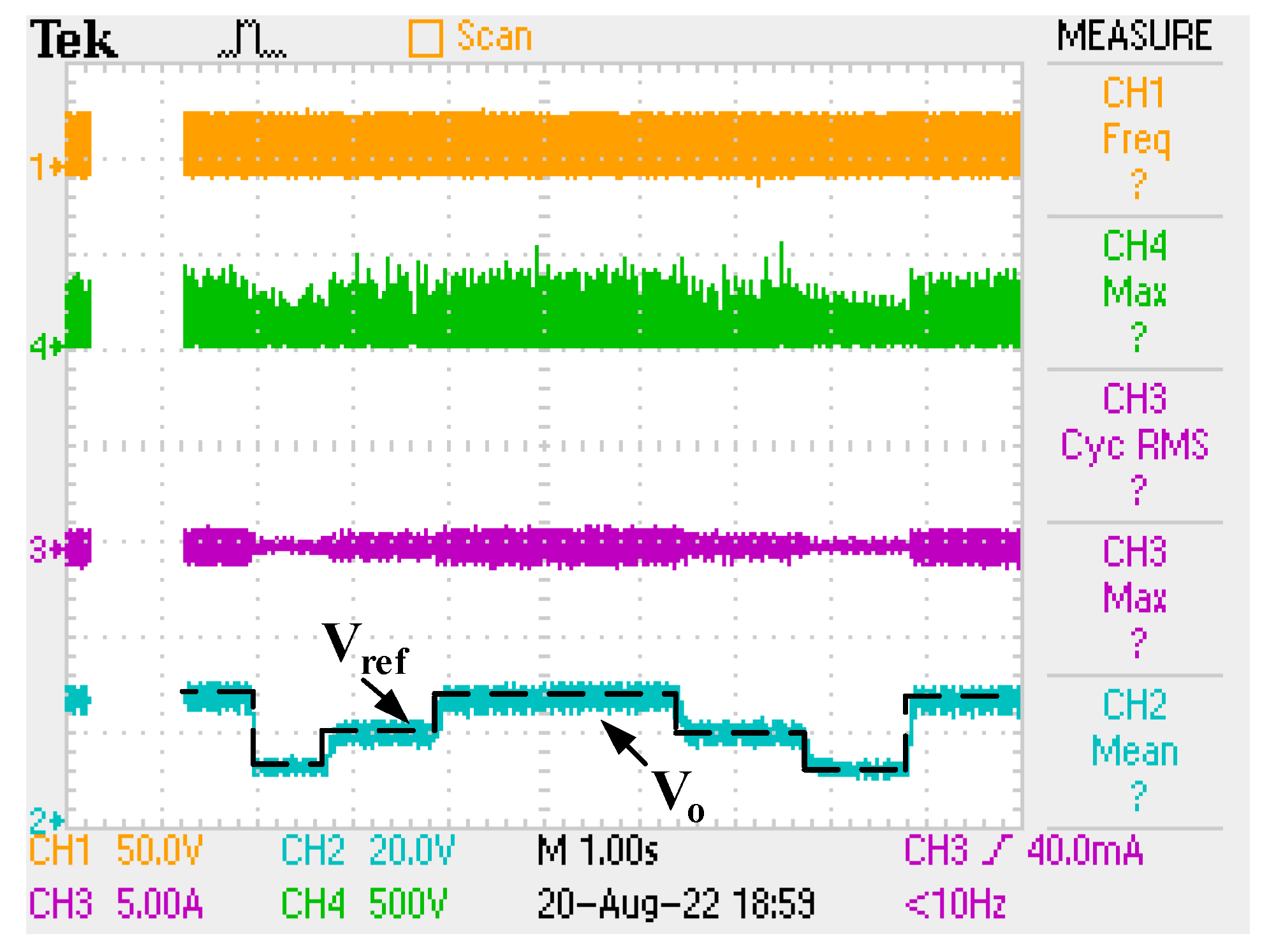
With different voltage reference values, measurement is realized as shown in
Figure 26. It is seen that the output voltage is regulated as desired with a maximum 1 s settling time and ±2 V steady-state error under the reference voltage change, that is from 25 V to 10 V, from 10 V to 20 V, from 20 V to 25 V, from 25 V to 20 V, from 20 V to 10 V, and from 10 V to 25 V.
The efficiency and THD regarding the loading of the converter using LC and LCL trap filters are given in
Figure 27. It is seen that the peak efficiency is 85% for the LCL trap filter and 83.4% for the LC filter. Regarding the THD of the grid current, the LCL trap filter provides 4.83% and the LC filter provides 6.71%. It is observed that the LCL trap filter ensures better results regarding THD and efficiency. Detailed analyses for the LC filter can be found in [
10].
Efficiency (η) is determined using (24) considering the whole system. While measuring the efficiency, the input AC voltage, current, and PF are measured and the active power (P
ac,in) is calculated, the output voltage and current are measured, and the output power (P
dc,out) is calculated.
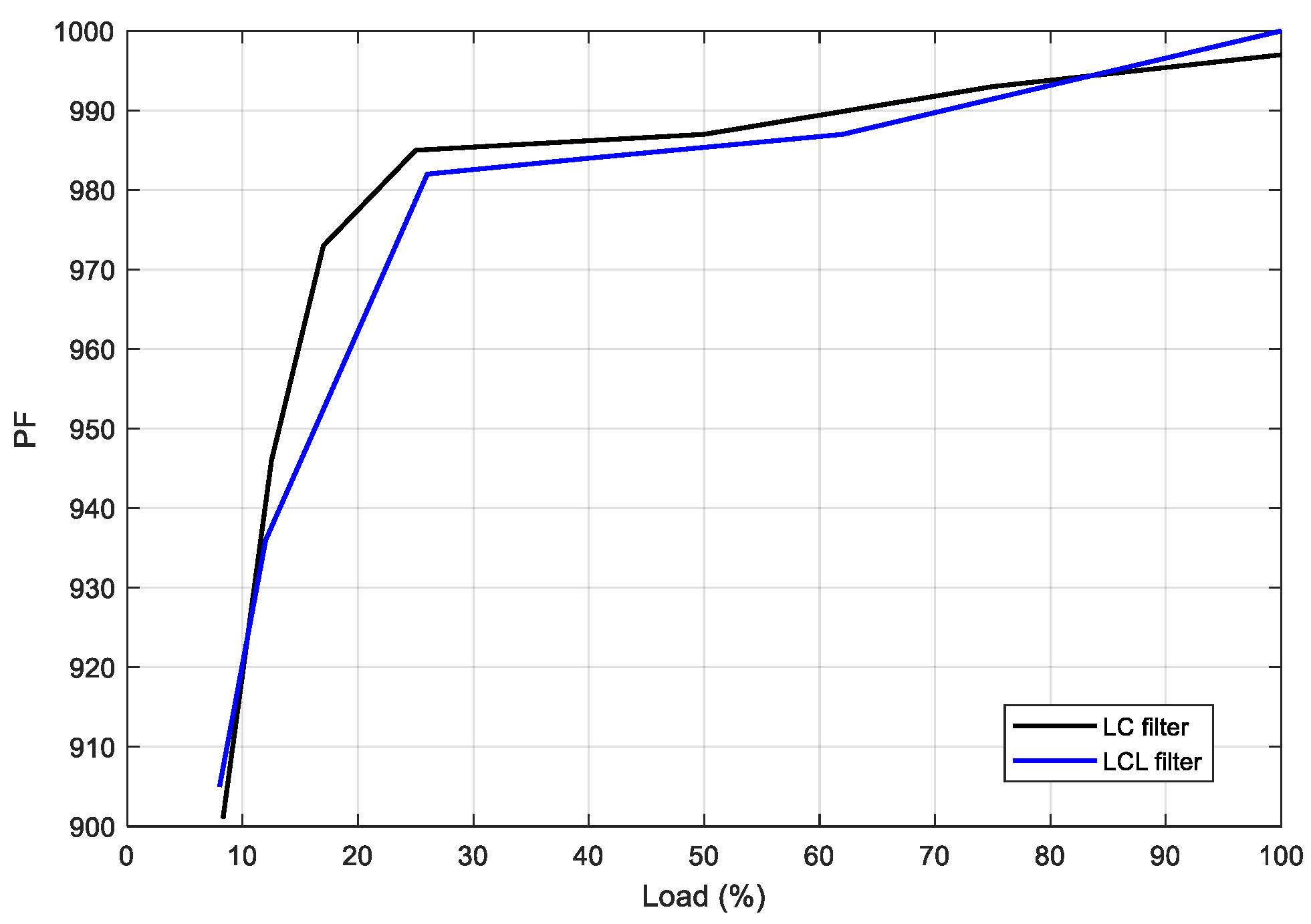
Further, in terms of loading, the PF comparison is given in
Figure 28 for the LC and LCL trap filters. It is seen that the peak PF is obtained at full load as 0.998 as in (16) with the LCL trap filter. With the LC filter, it is obtained as 0.997.
In addition, THDs are compared with the IEC 61000-3-2 C class standard [
31] and the LCL trap and LC filters for the first 39th harmonics, and the comparison is given in
Figure 29.
Loss analysis for the converter is conducted with the calculations in (25)–(46) for the LCL trap filter. The loss distribution includes DBR losses, output diode losses, copper losses, filter losses, switch losses, core losses, and output capacitor losses, with the same methodology as in [
3,
10,
32]. Also, (25)–(41) are the same as the calculation in [
10]. In the loss calculation, filter capacitance losses are neglected.
The loss diagram is given in
Figure 30 as percentages. It is seen that higher losses of the converter are power diode losses by percentage. It is assumed that choosing a low voltage drop Schottky diode increases the efficiency by 1–2%. Further, the snubber losses of the power switches and power diode are calculated as 0.82 W and 0.436 W, respectively.
By using the loss distribution in
Figure 30, the total losses are 10.5396 W for the LC filter and 10.16 W for the LCL trap filter. The output voltage of the LC filter is 25 V from [
10], and from
Figure 18 it is measured as 25.9 V for LCL trap filter. After taking the load as 12.5 Ω, efficiencies can be calculated as 82.5% for the LC filter and 84% for the LCL trap filter, which are close to the measured value of 85% for the operating point. An efficiency comparison of the present study with some of the studies in the literature for the same topology is given in
Table 5. According to the comparison, the present study has a moderate efficiency for this 50 W power level.
Filter cost is compared in
Table 6. For the LC filter, an ETD54 core is used with a 35.2 mH value. On the other hand, for the LCL trap filter, two ETD39 cores and one EE25 core are used with a total value of 20.05 mH. It can be concluded that the LCL trap filter is slightly more expensive than the LC filter regarding the core and capacitance values.
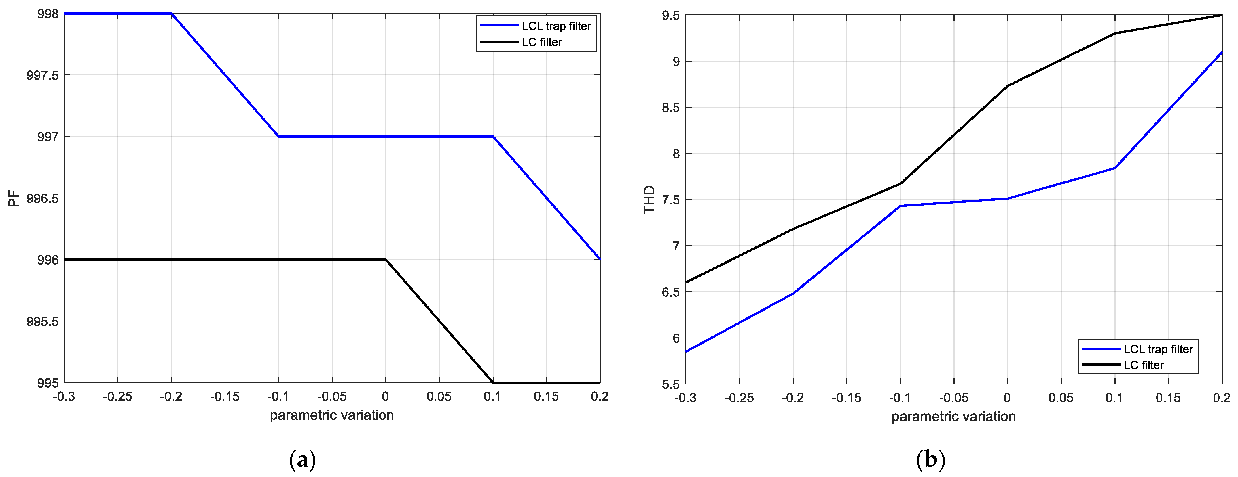
Moreover, both filters are investigated in terms of parametric variation in the filter components, the PF and THD are measured regarding small variation in the filter parameter, and the results are given in
Figure 31 after simulation for the ideal case of the transformer without considering power diode snubbers. The changes in the parameters are as follows for each filter: L
f1, L
f2, and L
f are changed by 0.1mH; C
f and C
t are changed by 1 nF; and L
t is changed by 10 μH. In the figure, (−) means a decrease in the parameters and (+) means an increase. In addition, initial values for the L
f1, L
f2, and L
f are taken as 9 mH, 10.2 mH and 35 mH, respectively.
It is seen in
Figure 31 that when the parametric variation increases, the PF begins to decrease and THD begins to increase. However, the decreases in the PF and THD by the parametric increment are not so drastic. On the other hand, the decreases in the PF and THD, especially the PF, are not surprising because one of the main conditions while choosing the filter in (1) is that C
f should be much lower than C
fmax. The increase in C
f breaks this condition, so it causes a reduction in the PF.
5. Discussion
In the present paper, a PFC isolated Ćuk converter using SiC MOSFET in DCM with an LCL trap filter is presented, which is the unique contribution of the paper because in the literature no PFC converter using an LCL trap filter has been presented.
In the simulation study, exact values of the capacitances of the transformer including interwinding and winding capacitances could not be added; instead, estimated capacitance values are used. These capacitance values affect the switch voltage stress. Furthermore, the analytical calculated values of transformer inductances, coupling coefficient, and mutual inductance are used in the simulation. To have an exact comparison for the transformer model, measured values of the implementation are better, especially for primary, secondary, and interwinding capacitances. However, the scope of this study is not to derive an exact model of the transformer. Further, simulations are repeated using a voltage regulator at the output of the converter as a nonlinear load with the exact model of SiC MOSFET in the application. The results of using a nonlinear load do not deviate much from those obtained using a linear load; the difference is maximum 0.003 for the PF and 2.9% for THD regarding both filters from
Table 4. In addition, the voltage stress of the switch is higher in the simulation study except in the ideal transformer model and application results. The output voltage with the LCL trap filter is higher than that with the LC filter by up to 1 V. Moreover, the simulation study is conducted just for an open loop.
The application of the converter using LCL trap and LC filters is conducted. Modeling of the converter with an LCL trap filter in a DCM model is performed in terms of large and small signals. Further, large- and small-signal models with or without an LCL trap filter are compared using d variation, and similar results are obtained, proving that the modeling is accurate. Moreover, a large-signal model has a smaller steady-state error compared to the small-signal model. In addition, in the application, the output voltage of the converter is regulated by a PI controller designed considering the filter effect in the transfer function by the root locus method. As a result of the measurement, output voltages are regulated as desired with a maximum 1 s settling time and ±2 V steady-state error under reference changes. Moreover, as a control characteristic for stability the LCL trap filter has a much higher gain than the LC filter. Further, the application is tested with nonlinear and linear loads separately as in the simulation; as a nonlinear load, a voltage regulator is used, and as a linear load, resistive loads are used. Regarding load type, for the LC filter the results of the THD and PF become worse with 0.002 for the PF and 0.2% for the THD under a nonlinear load compared to a linear load. For the LCL trap filter, the THD improves by 0.23% with a nonlinear load than with a linear load. However, for the nonlinear load operation, the duty cycle is increased by 0.02 to increase the output voltage compared to the linear load. However, the main results regarding the PF and THD values are slightly better in the applications than in each of the simulations.
A comparison of LCL trap and LC filters is also presented in the study for both simulation and application results. Regarding the simulations in
Table 4, in each case of the simulations, the LCL trap filter gives better results for the THD and PF except for the resistive load with the model in
Figure 17 with a 0.001 PF and a 0.14% THD difference. A comparison is also performed with the application for the PF and THD, and the efficiency of the LCL trap filter is higher than that of the LC filter. In addition, the efficiency value presented with the LCL trap filter is acceptable for its power rating regarding the literature presented in
Table 5. A comparison with the standard is also presented and each filter meets the standards. Further, a cost comparison is presented in
Table 6, and it can be concluded that the LCL trap filter is slightly more expensive than the LC filter.
Parametric variation in the filter components is considered in the study as well. As a result of the simulation regarding parametric variation, when the parametric variation has a tendency to increase in the parameters, the PF and THD begin to worsen in relation to the increment rate. On the other hand, when the parametric variation has a tendency to decrease in the parameters, the PF and THD begin to improve with the decrement rate. The result is not so surprising because of the condition of choosing the Cf. The filter capacitor should have a value much lower than the Cfmax.
