Article

Universal Input Single-Stage High-Power-Factor LED Driver with Active Low-Frequency Current Ripple Suppressed

1
Department of Electrical Engineering, National Taipei University of Technology, No. 1, Sec. 3, Zhongxiao E. Rd., Taipei 10608, Taiwan
2
Department of Electrical Engineering, Feng Chia University, No. 100, Wenhwa Road, Seatwen, Taichung 40724, Taiwan
*
Author to whom correspondence should be addressed.
Energies 2024, 17(1), 183; https://doi.org/10.3390/en17010183
Submission received: 17 November 2023 / Revised: 14 December 2023 / Accepted: 18 December 2023 / Published: 28 December 2023
(This article belongs to the Special Issue Optimal Design and Application of High-Performance Power Converters)

Abstract

:
In this paper, a light-emitting diode (LED) driver with a high power factor (PF) and low-frequency current ripple suppression over a wide input range is presented, and a flyback converter is designed to operate in the discontinuous conduction mode (DCM), with a digital controller used to keep the duty cycle constant for half of the utility cycle under a fixed load and input voltage. This method ensures that the input current is in phase with the universal input voltage, thus achieving a high power factor without utilizing feedforward control. Furthermore, on the secondary side, the time of the zero point of the utility voltage can be attained so that the duty cycle can be updated at this time. In addition, a simple auxiliary circuit is connected parallel to the output side to absorb the excess output current of the flyback converter or to release the current to the load to make up for the shortage of the output current of the flyback converter so that the low-frequency ripple of the output current can be inhibited. There are only two current-detecting resistors used in this study: one is the output current-sensing resistor of the flyback converter, and the other is the output current-sensing resistor of the auxiliary circuit.

1. Introduction

In actual power applications, most electronic products are not purely resistive loads but may contain inductive loads, capacitive loads, or non-linear loads. However, when a sinusoidal voltage is input, to consider the consumption of generic and specific (pure inductive and capacitive) inductances, the pure resistive load consumes energy, which is called real power, and the purely inductive and purely capacitive loads only store or release energy, which is called reactive power. But when a sinusoidal voltage is input and the load is non-linear, only the fundamental wave component has power output, and the others are harmonics. Therefore, increasing the power factor (PF) of the consumer by using the AC/DC converter as the energy interface can save energy and reduce the total harmonic distortion (THD) [1].
The active power factor correction circuits can be divided into two-stage and single-stage types. In recent years, products with two-stage power factor correction circuits have been gradually developed, and numerous papers and research results have been published on the subject. Although the two-stage power factor correction circuit has a high power factor, relatively low input current with high harmonics, and stable output voltage, the two-stage type has one more energy conversion process and one more control circuit than the single-stage type, which results in more components, more complex circuits, a larger size and weight, and a higher cost.
The conventional single-stage power factor correction converter uses a single converter to realize the power factor correction. It is the most commonly used structure for low-wattage LED luminaires in the industry because of its high power factor and low total harmonic distortion.
Related studies have proposed solutions to the problem of low-frequency ripple. In [2], a valley-filling filter circuit is used, and in [3], an auxiliary energy storage circuit is used to improve the low-frequency ripple of the output voltage, but this method shortens the on-time of the input current at the expense of the power factor.
In [4], an auxiliary circuit, which is powered by the battery, is added to the main power stage to reduce the low-frequency ripple of the output voltage by controlling the active switch in the auxiliary circuit to generate a current in the opposite direction of the current ripple of the main power stage.
In [5], the same switch is used to integrate a boost converter and a flyback converter into a single-stage converter, which relies on the energy storage capacitor between the two converters to decouple the low-frequency components and is able to recover the leakage current to improve efficiency. However, the drawback is that the energy still needs to be converted twice, which will increase the loss, and the experimental waveform shows a lack of ripple cancellation capability to some extent.
In [6], half-bridge active switches are used with soft switching to reduce losses. However, the drawback is that two transformers and one inductor are used, thereby increasing the overall weight and volume of the circuit. In addition, the experimental output current is lacking to a certain degree in ripple cancellation capability.
The literature [7] uses a simple two-stage structure and creates a DC voltage across a capacitor to compensate for the lack of a utility power supply and achieve low-frequency ripple cancellation. However, the drawback is that when the input voltage is less than the voltage across the capacitor, the input current will be flat, which will seriously damage the input current waveform and affect the power factor and total harmonic distortion.
In [8], the step-up converter, step-down converter, and flyback converter are integrated into a single-stage converter, and the same switch is used to operate the circuit, which simplifies the control and reduces the losses caused by the switch. However, the drawback is that the energy must be converted twice, which increases the overall loss, and the linear regulator is used in the back stage, which can suppress low-frequency ripple but significantly reduces the overall efficiency.
Reference [9] shows that the input adopts a bridgeless structure, which can reduce the conduction loss caused by the traditional full-bridge rectifier, and the half-bridge switches have soft switching to reduce the switching loss and further improve the efficiency. And the front and back stages are integrated into a single-stage structure through the same switch used, reducing the number of switches. However, the drawback is that since the input is the AC power source, it is necessary to determine the positive and negative status of the input voltage to activate the switch given by the main control force.
Reference [2] shows the LED driver. The advantage of this driver is that the main power stage is a step-down converter, so the structure is simple and efficient, and the proposed average current control with valley-filling power factor correction is used to remove low-frequency ripple currents.
As shown in [10], two opposite LCL output voltages are generated, so if the output capacity requirement is reduced, the LCL current can still be suppressed, and the secondary output voltage is minimized to reduce the loss and harmonic component of the input current. However, the drawback is that the auxiliary circuit will cause the input current to generate a zero-current plateau when the input voltage is close to zero, which increases THD, and the control of the switch requires circuit status feedback and complex judgment.
The circuits shown in [11,12] are similar, but they differ in the control strategy. The advantage of [11] is that the circuit uses a fixed on-time step-down converter as the auxiliary circuit, which has fast load transient response and is capable of eliminating low-frequency ripple across the load voltage and minimizing the secondary-side power conversion by depressing the secondary-side output voltage to optimize efficiency. However, the drawback is that the coupling inductor of the flyback converter requires multiple windings, which are not easy to manufacture because they must be tightly wound, and some power is still converted twice, resulting in lower efficiency. The advantage of [12] is that after the input power is at its maximum value, the energy is transferred only through the second winding of the flyback converter until the input power is lower than the output power. Then, the energy is transferred through the third winding and the step-down converter so that the energy can be drawn from the storage capacitor to make up for the shortage of the input power. However, the drawback is that this circuit is not able to store the excess energy when the input power is greater than the output power, resulting in a surge current at the output.
As shown in [13], the output voltage of the flyback converter is connected in series with the output voltage of the full-bridge inverter to eliminate the low-frequency voltage ripple without the use of electrolytic capacitors, and the auxiliary winding or loss compensation is used to avoid the imbalance between the stored and released energy of the full-bridge inverter due to the loss in the line, which leads to the inability to completely eliminate the low-frequency voltage ripple. However, the disadvantage of this circuit is that it is a high-voltage output with LEDs in series up to 150 V. The ground of the auxiliary capacitor voltage is the same as that of the output voltage, which makes it more complicated to realize the voltage feedback control.
As shown in [14,15], the whole system is completed in a nearly single-stage circuit, and only one inductive component is used to reduce the circuit size and weight; instead of using the electrolytic capacitor, the thin-film capacitor and the multi-layer ceramic capacitor (MLCC) are adopted to obtain a longer circuit life and a wider operating temperature range. Moreover, some power semiconductors have zero current switching (ZCS) at cutoff to reduce the switching losses of the overall system. However, the drawback is that the main switch is connected in series with the diode, so the conduction loss is higher. For the energy release mode in [14], the energy in the storage capacitor is first stored in the coupling inductor, and then the coupling inductor transfers the energy to the load, whereas for the energy release mode in [15], the storage capacitor directly transfers part of the energy to the load, and the excess energy is stored in the coupling inductor. From this, it can be known that the conversion loss in [15] is less than that in [14].
Therefore, this paper aims to develop a single-stage LED driver with low-frequency current ripple suppression and a high power factor over a wide input range. The basic principle is to combine the flyback converter and the synchronously rectified boost converter. By using the active switching of the synchronously rectified boost converter to store and release energy and to deploy the output power of the flyback converter, the low-frequency ripple can be suppressed.

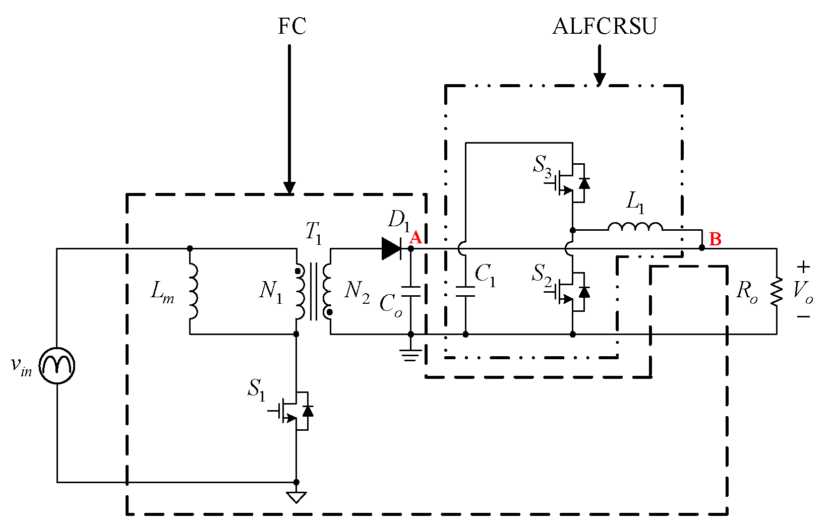
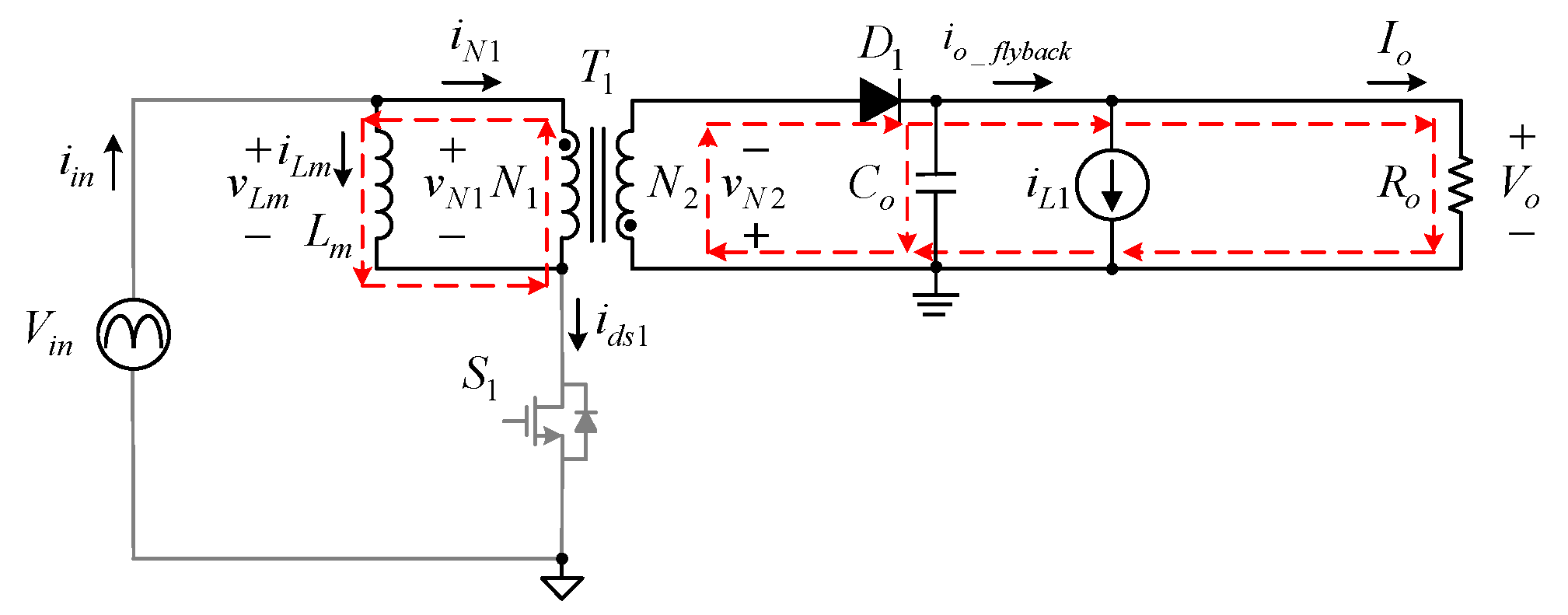
2. Analysis of the Proposed Circuit

Figure 1 shows the proposed circuit structure, which is composed of an active low-frequency current ripple suppression unit (ALFCRSU) combined with a flyback converter (FC). The components of the FC are one switch S1, one diode D1, one coupled inductor T1, and one output capacitor Co. The components of the ALFCRSU are two switches S2 and S3, one capacitor C1, and one inductor L1. The secondary coil of the coupled inductor T1 is represented by N1, and the secondary coil is represented by N2. The load is represented by the output resistance, Ro.
The relevant symbols are shown in Figure 2 and defined as follows:
(1)
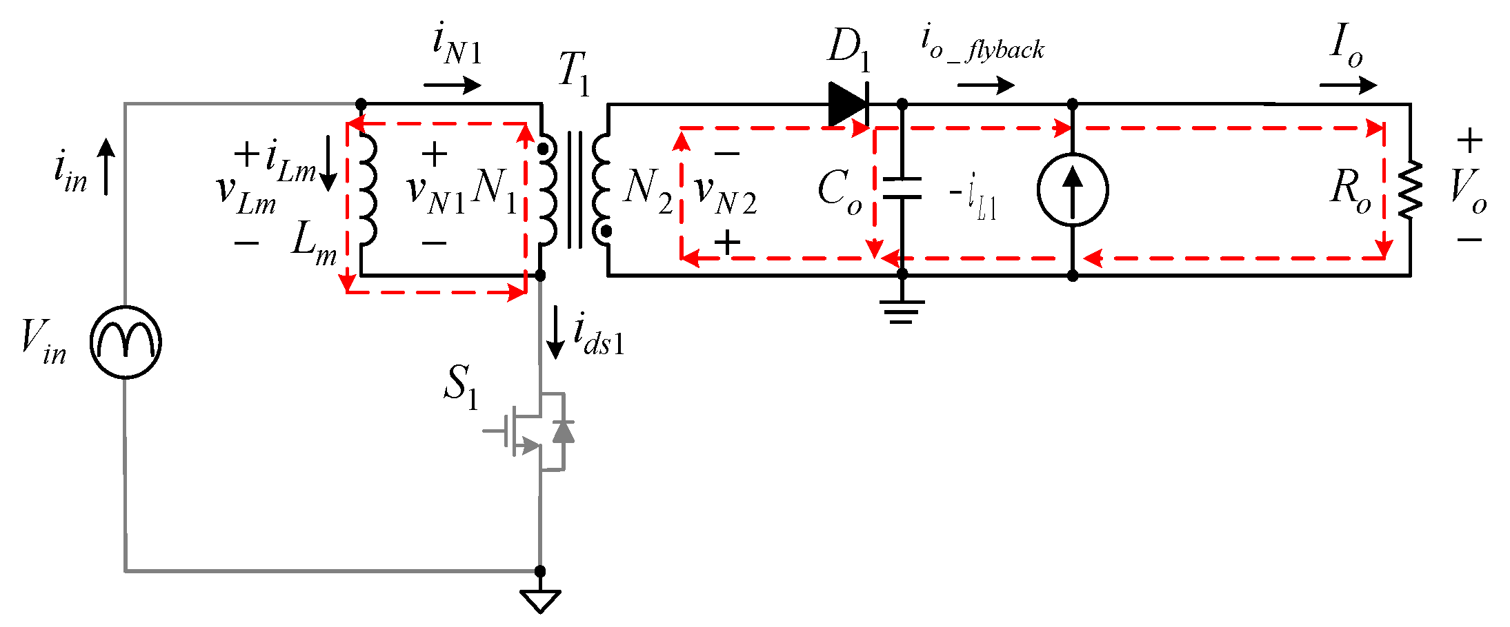
vin is the input voltage, Vo is the output voltage, and iin is the input current.
(2)
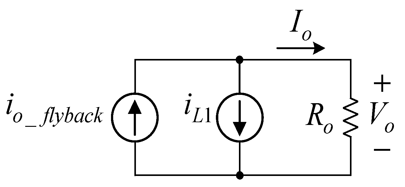
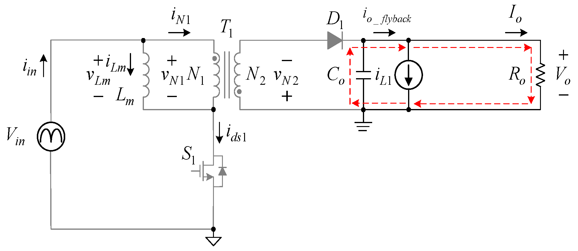
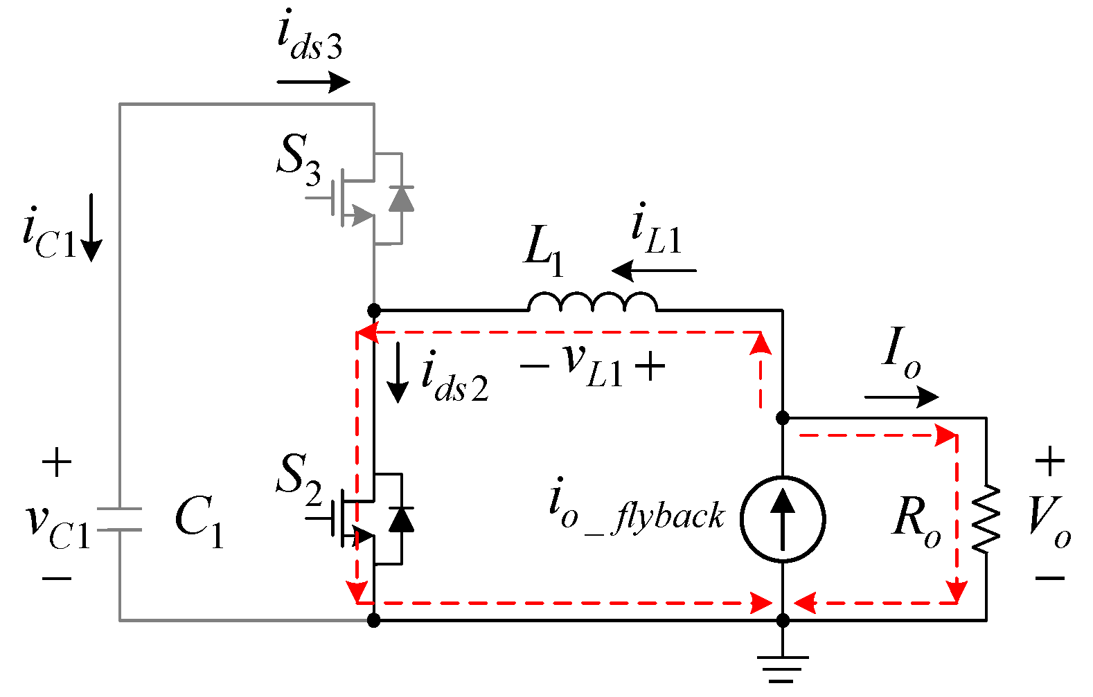
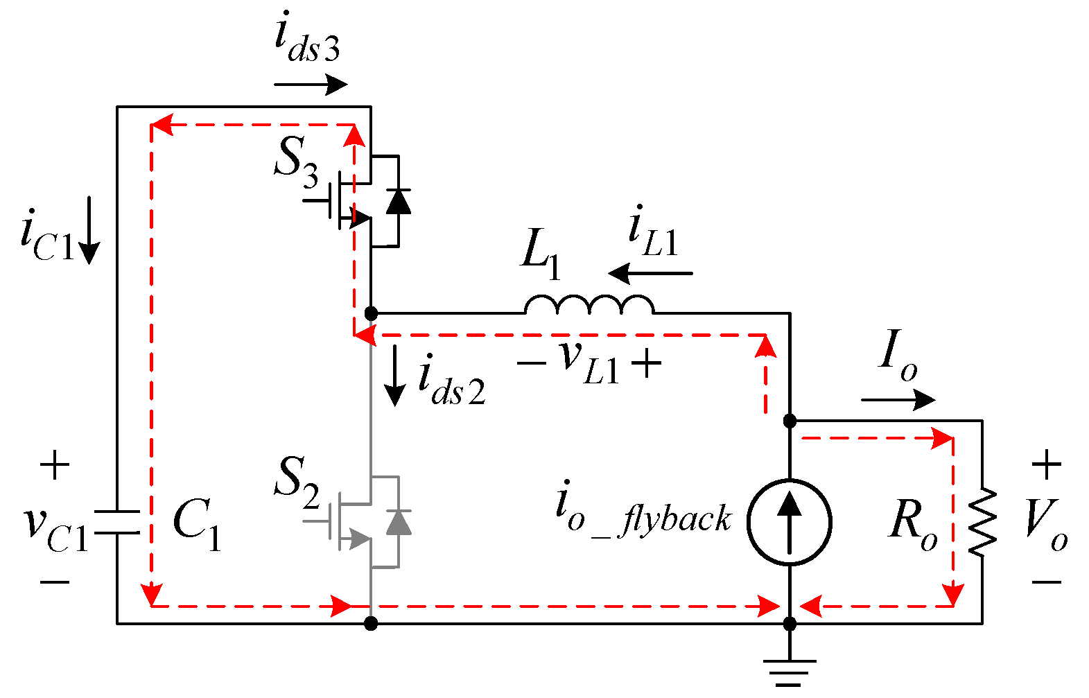
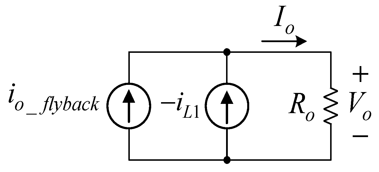
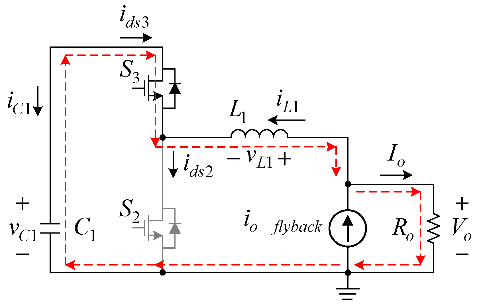
io_flyback is the current flowing from point A to point B, iD1 is the current in the diode D1, ids1 is the current in the switch S1, ids2 is the current in the switch S2, ids3 is the current in the switch S3, iN1 is the current in the coil N1, iLm1 is the current in the magnetizing inductor Lm, iL1 is the current in the inductor L1, iC1 is the current in the capacitor C1, and Io is the current flowing through the output resistor Ro.
(3)
vLm is the voltage across the magnetizing inductor Lm, vN1 is the voltage across the coil N1, vN2 is the voltage across the coil N2, vL1 is the voltage across the inductor L1, and vC1 is the voltage across the capacitor C1.
For convenience of analysis, the following definitions and assumptions are made first:
(1)
The small-ripple approximation method is used for analysis in the steady state.
(2)
The FC operates in the discontinuous conduction mode (DCM), and the ALFCRSU operates in the continuous conduction mode (CCM).
(3)
The switching period is Ts1, the on-time of the switch S1 is Dx1Ts1, the cutoff time of the switch S1 is (1 − Dx1)Ts1, the switching period of the switches S2 and S3 is Ts2, the on-time of the switch S2 and the cutoff time of the switch S3 are DyTs2, the cutoff time of the switch S2 and the on-time of the switch S3 are (1 − Dy)Ts2; Ts1 is much larger than Ts2, and the blanking time is neglected.
(4)
The FC and the ALFCRSU are independent of each other in terms of operation timing, so they can be analyzed separately.
(5)
The switches are regarded as ideal.
(6)
The inductor L1, the coupled inductor T1, and the capacitors Co and C1 are not considered for their parasitic resistance.
(7)
The value of the output capacitor Co is large enough to keep the voltage across it at a constant value, Vo.
(8)
The coupling coefficient of the couped inductor T1 is one, i.e., leakage inductances are not considered.
(9)
Since the switching frequency is much larger than the line frequency, vin can be considered a DC value over one or more switching periods. The proposed ALFCRSU has two operating states over the line radian frequency ωL, as shown in Figure 3. In addition, state I occurs when the ALFCRSU stores energy, whereas state II occurs when the ALFCRSU releases energy.
(10)
The proposed FC and ALFCRSU both operate under negative feedback current control.
(11)
The load current is defined as Io.

2.1. ALFCRSU Operating Concept

The input voltage vin and the input current iin are defined as
v i n = V m sin ( ω L t )
i i n = I m sin ( ω L t )
where Vm and Im are the amplitudes of vin and iin, respectively.
The instantaneous input power pin is defined as
p i n = V m sin ( ω L t ) × I m sin ( ω L t ) = V m I m × 1 cos ( 2 ω L t ) 2 = V m 2 × I m 2 × [ 1 cos ( 2 ω L t ) ] = V r m s I r m s × [ 1 cos ( 2 ω L t ) ] = P i n [ 1 cos ( 2 ω L t ) ]
where Vrms and Irms are the root-mean-square values of vin and iin, respectively.
It is assumed that the efficiency is one, namely, that the instantaneous input power pin is identical to the instantaneous output power po, and hence, the average input power Pin is identical to the instantaneous output power Po, and the current io_flyback can be expressed as
i o _ f l y b a c k = p o V o = P o V o × [ 1 cos ( 2 ω L t ) ] = I o × [ 1 cos ( 2 ω L t ) ]
From (4), the effect of ALFCRSU can be achieved by controlling the inductor current iL1 as follows:
i L 1 = i o _ f l y b a c k I o = I o × cos ( 2 ω L t )
Based on the above assumptions, since the operations of the FC and ALFCRSU are independent of each other, their related waveforms can be discussed separately. In the following analysis, based on the ALFCRSU, there are two operating states.

2.2. Operating Behavior of FC and ALFCRSU in State I

In State I, the ALFCRSU stores energy. Figure 4 shows the equivalent circuit of the proposed topology. The associated equation is
I o = i o _ f l y b a c k i L 1 ,   i L 1 > 0
In this state, iL1 will absorb the output current io_flyback of the FC minus the load current Io.

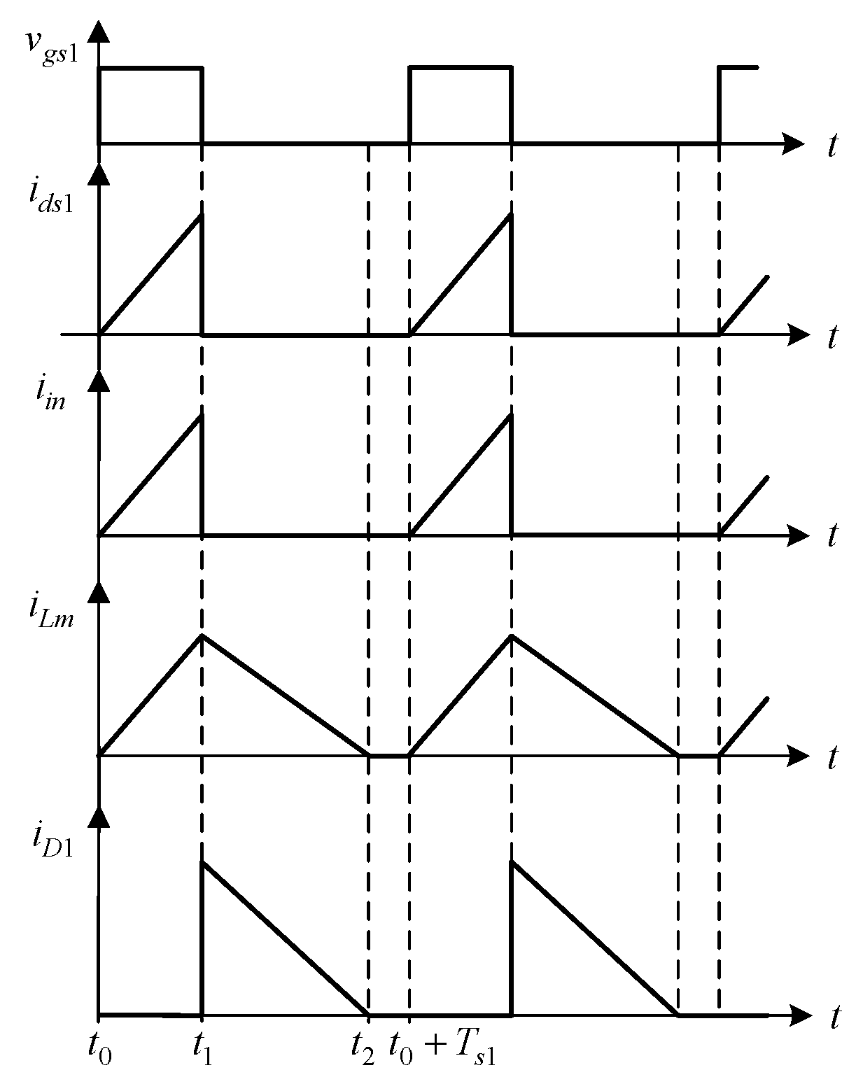
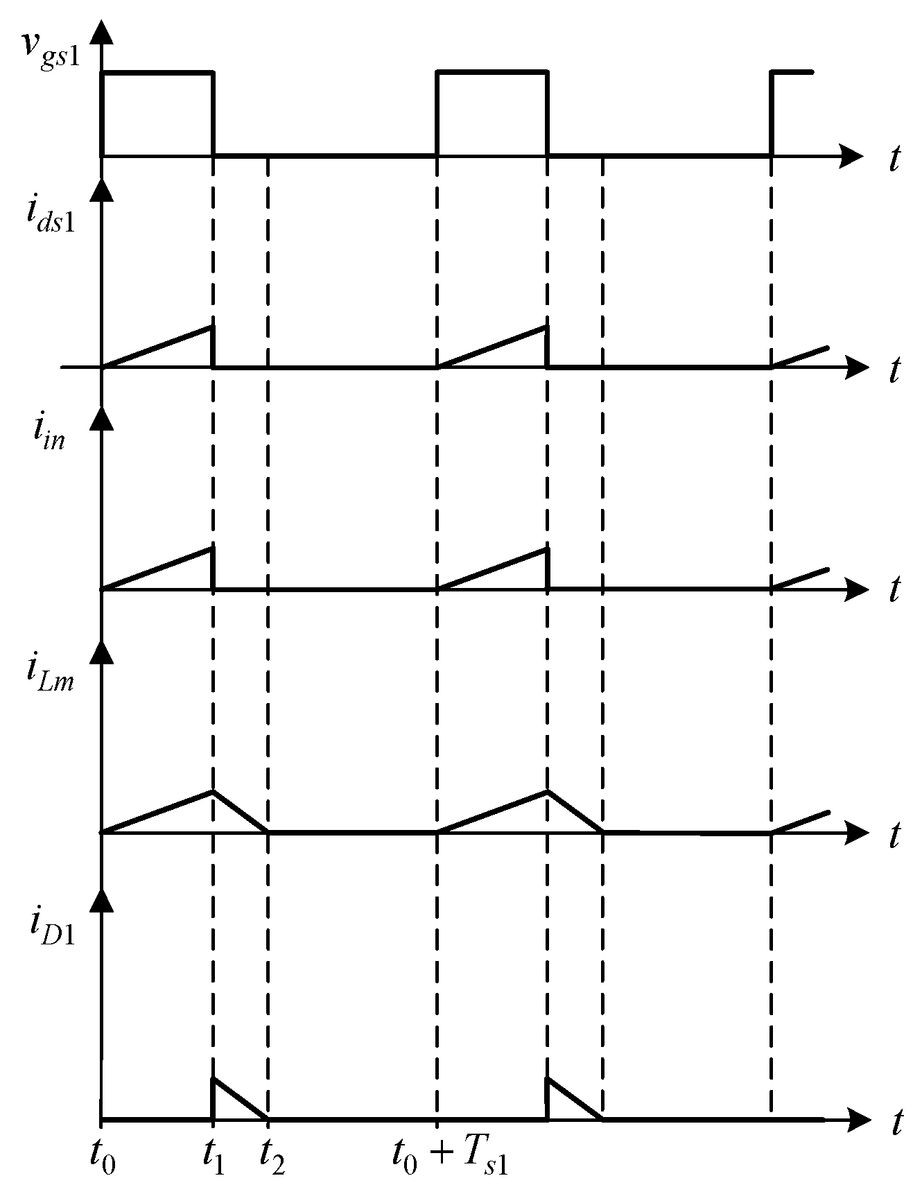
2.2.1. FC Operating Principle in State I

The FC operates in the DCM, so there are three modes to be described, as shown in Figure 5.

Mode 1: [t0 ≤ t ≤ t1]

As shown in Figure 5 and Figure 6, the switch S1 is on. During this mode, the diode D1 is cut off. At the same time, the voltage across the magnetizing inductor Lm is the input voltage Vin, so Lm is magnetized. The output capacitor Co is discharged to provide energy to the load Ro and ALFCRSU.

Mode 2: [t1 ≤ t ≤ t2]

As shown in Figure 5 and Figure 7, the switch S1 is cut off. During this mode, the diode D1 is turned on. At the same time, the voltage across the magnetizing inductor Lm is −nVo, so Lm is demagnetized, and the energy stored in Lm is transferred to the output and ALFCRSU via the secondary winding N2.

Mode 3: [t2 ≤ t ≤ t0 + Ts]

As shown in Figure 5 and Figure 8, the switch S1 is cut off. During this mode, the diode D1 is cut off. At the same time, the magnetizing inductor Lm has no energy, and only the output capacitor Co is discharged to provide energy to the load Ro and ALFCRSU.

Voltage Gain of the FC in State I

For the FC to be considered, the duty cycle Dx1 is updated every half utility cycle. The average power of the half utility cycle must be used to calculate the actual voltage gain, which is defined as the output voltage Vo divided by the maximum value of vin, called Vm. By assuming the efficiency equals one, the following equation can be obtained:
V m 2 × D x 1 2 × T s 1 4 × L m = V o 2 R o V o V m = R o × D 2 × T s 1 4 × L m = D x 1 2 × R o × T s 1 L m
Also,
V m = 2 × V a c
Therefore, the relationship between the output voltage Vo and the root-mean-square (RMS) value of vac, called Vac, is
V o V a c = D x 1 × R o × T s 1 2 × L m

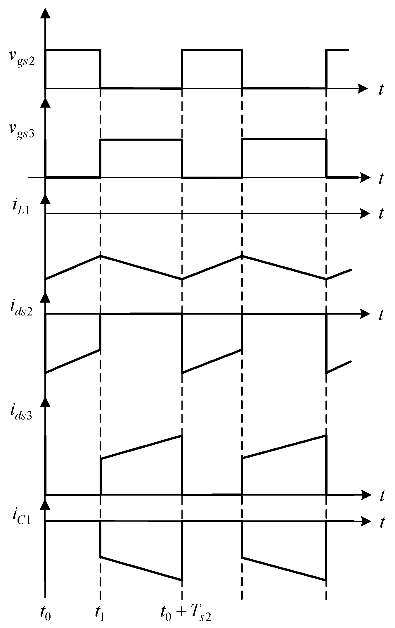
2.2.2. ALFCRSU Operating Principle in State I

The ALFCRSU operates in the CCM, so there are two modes to be described, as shown in Figure 9.

Mode 1: [t0 ≤ t ≤ t1]

As shown in Figure 9 and Figure 10, switch S2 is on and switch S3 is off. At this time, the voltage across inductor L1 is the output voltage Vo, so L1 is magnetized. The FC provides energy to L1 and the load Ro.

Mode 2: [t1 ≤ t ≤ t0 + Ts]

As shown in Figure 9 and Figure 11, the switch S2 is cut off and the switch S3 is on. At the same time, the voltage across the inductor L1 is VovC1, so L1 is demagnetized. The capacitor C1 obtains energy from L1 and the FC, so it is charged, and the FC also provides energy to the load Ro.

Voltage Gain of the ALFCRSU in State I

Since the voltage across the inductor L1 over one switching cycle in steady state must obey the volt-second balance, the following equation can be obtained:
D y × V o + ( 1 D y ) × ( V o V C 1 ) = 0
By rearranging (10), the corresponding voltage gain can be obtained:
V C 1 V o = 1 1 D y

2.3. Operating Behavior of FC and ALFCRSU in State II

In state II, the ALFCRSU stores energy. Figure 12 shows the equivalent circuit of the proposed topology. The associated equation is
I o = i o _ f l y b a c k i L 1 ,   i L 1 < 0
In this state, iL1 will release current to compensate for the output current io_flyback of the FC and to provide energy to the load current Io.

2.3.1. FC Operating Principle in State II

The flyback converter operates in the DCM, so there are three modes to be described, as shown in Figure 13.

Mode 1: [t0 ≤ t ≤ t1]

As shown in Figure 13 and Figure 14, the switch S1 is on. During this mode, the diode D1 is cut off. At the same time, the voltage across the magnetizing inductor Lm is the input voltage Vin, so Lm is magnetized. The output capacitor Co, together with the ALFCRSU, is discharged to provide energy to the load Ro.

Mode 2: [t1 ≤ t ≤ t2]

As shown in Figure 13 and Figure 15, the switch S1 is cut off. During this mode, the diode D1 is turned on. At the same time, the voltage across the magnetizing inductor Lm is −nVo, so Lm is demagnetized. The energy stored in Lm is transferred to the secondary winding N2, and together with the ALFCRSU, it is supplied to the output, so the output capacitor Co is charged.

Mode 3: [t2 ≤ t ≤ t0 + Ts]

As shown in Figure 13 and Figure 16, the switch S1 is cut off. During this mode, the diode D1 is cut off. At the same time, the magnetizing inductor Lm has no energy, and the output capacitor Co, together with the ALFCRSU, is discharged to provide energy to the load Ro.

Voltage Gain of FC in State II

The corresponding voltage gain is the same as that shown in (9).

2.3.2. ALFCRSU Operating Principle in State II

The ALFCRSU works in the CCM, so there are two modes to be described, as shown in Figure 17.

Mode 1: [t0 ≤ t ≤ t1]

As shown in Figure 17 and Figure 18, the switch S2 is on and the switch S3 is off. During this mode, the voltage across the inductor L1 is the minus output voltage Vo, so L1 is reverse demagnetized. At the same time, the flyback converter and L1 provide energy to the load Ro.

Mode 2: [t1 ≤ t ≤ t0 + Ts]

As shown in Figure 17 and Figure 19, the switch S2 is cut off and the switch S3 is on. During this mode, the voltage across the inductor is V o v C 1 , so L1 is reverse magnetized. The capacitor C1 provides energy to the inductor L1 and the load Ro so it is discharged, and the FC also provides energy to the load Ro.

Voltage Gain of the ALFCRSU in State II

Since the voltage across the inductor L1 over one switching cycle in the steady state must obey the volt-second balance, the following equation can be obtained:
( 1 D y ) × V o + D y × ( V o V C 1 ) = 0
By rearranging (13), the corresponding voltage gain can be obtained:
V o V C 1 = D y

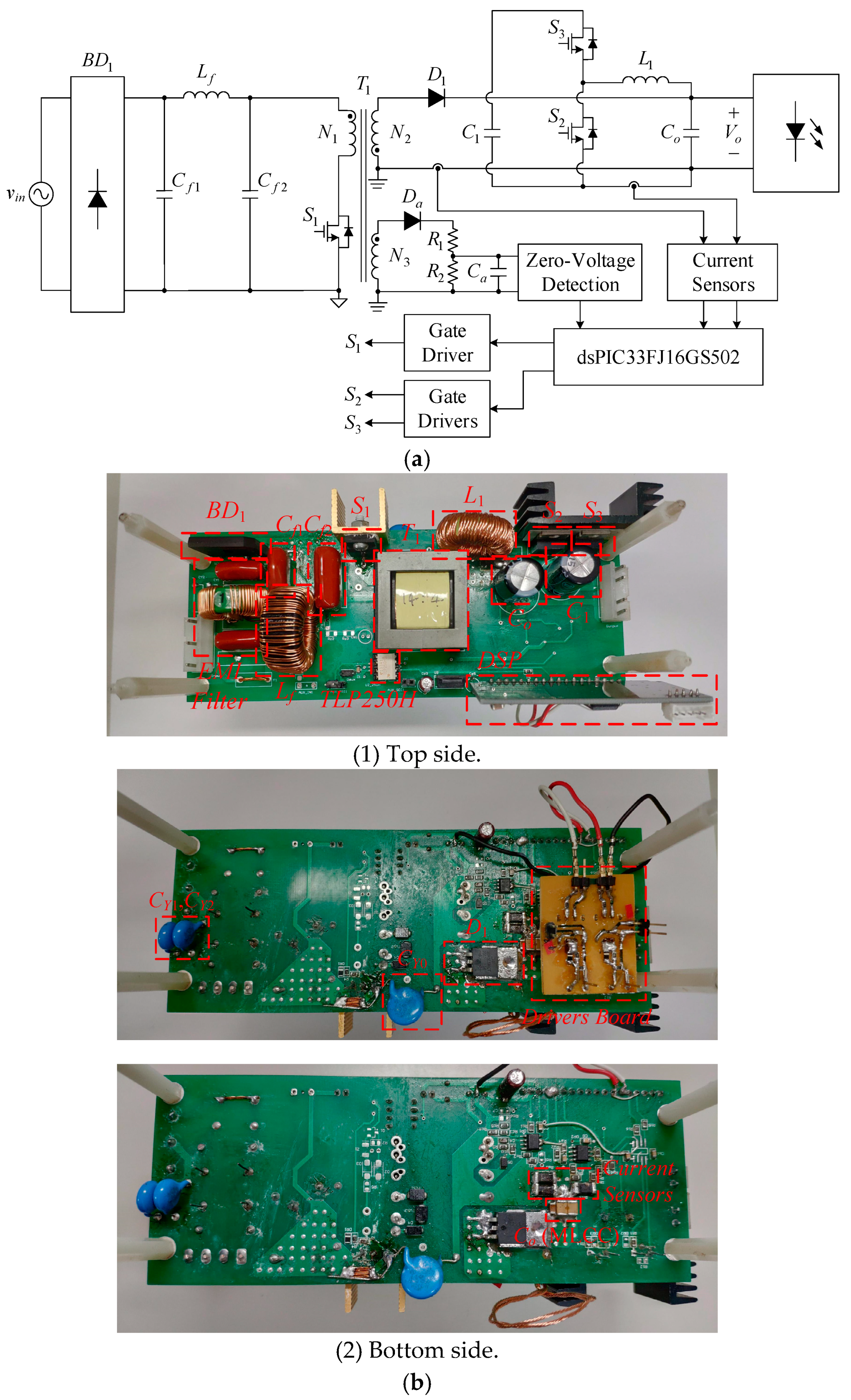
3. System Configuration along with Circuit Component Specifications

Figure 20a shows a block diagram of the system. The system configuration consists of the main circuit and the feedback control circuit. The main circuit is composed of the FC and ALFCRSU. In the feedback circuit, the analog signal of the output current is obtained from the current sensor, and then the analog-to-digital converter (ADC) inside the dsPIC33FJ16GS502 converts the analog signal into the digital signal, and the zero-voltage detection generates the trigger signal. The control force created from the dsPIC33FJ16GS502 is then used to regulate the switches after the isolated gate drivers. In addition, Figure 20b shows a photo of the experimental setup. In addition, Table 1, Table 2 and Table 3 display the LED specifications, LED driver specifications and summary of the component specifications for this system, respectively.

4. Control Strategy

4.1. Input Voltage Waveform Restoration Circuit

As shown in Figure 21, when the switch S1 is on, the input voltage vin is mapped from the primary winding N1 of the coupled inductor T1 to the third winding N3, and the voltage is built up across the capacitor Ca due to the conduction of the diode Da. Since the relationship between N2 and N3 is opposite in polarity, the diode Da is cut off. The above-mentioned input voltage waveform restoration circuit can directly obtain the input voltage information from the coupled inductor T1 to realize waveform restoration, as well as exclude the output voltage component.

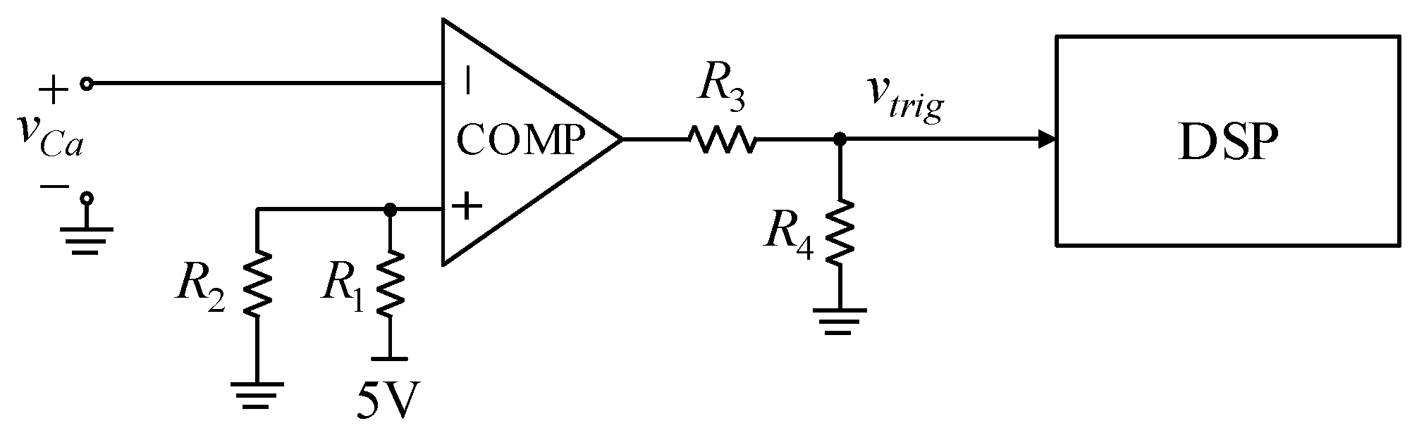
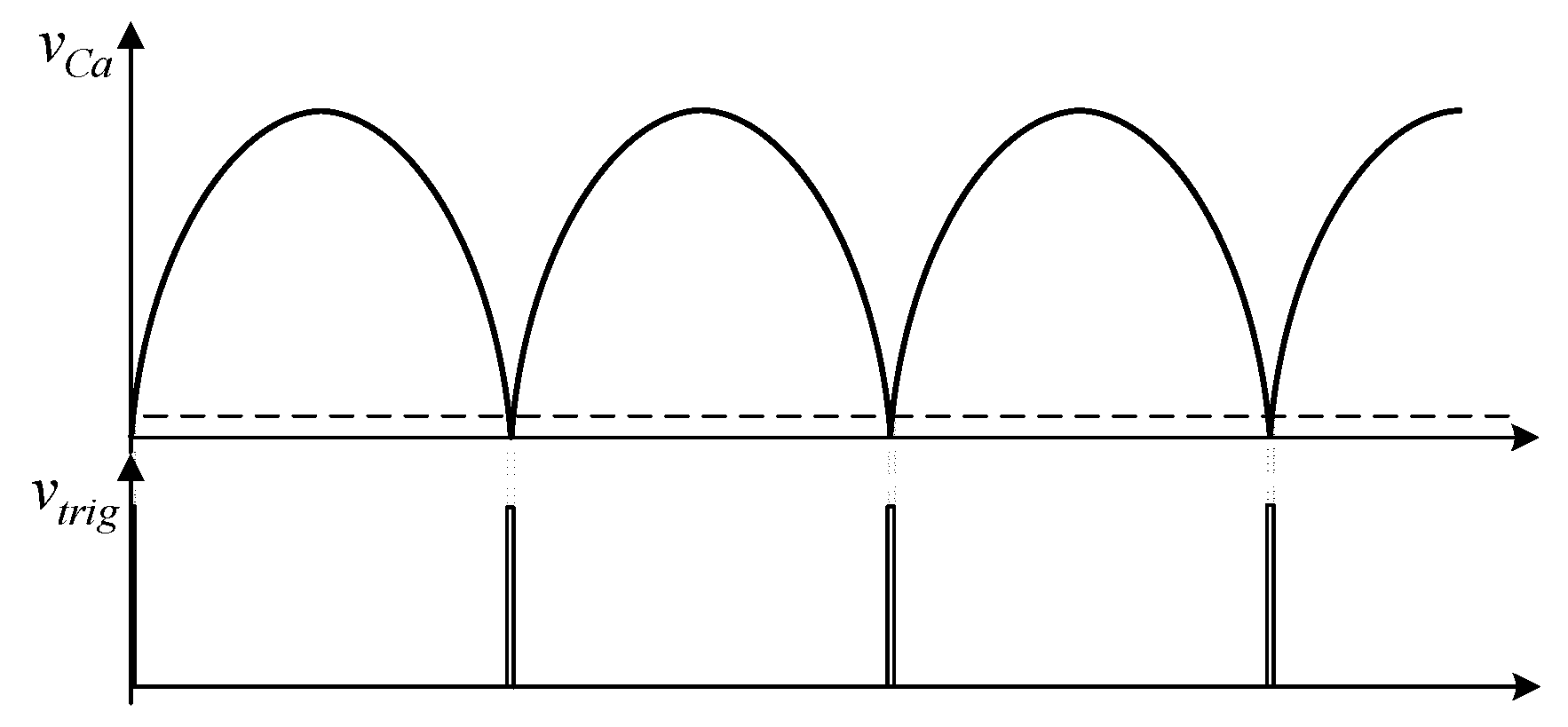
4.2. Zero-Voltage Detection

The zero-voltage detection circuit is displayed in Figure 22. Therefore, the restoration waveform is compared with the voltage level of about 1.34 V to generate the trigger signal, called vtrig, as shown in Figure 23, and this signal will be sent to the DSP.

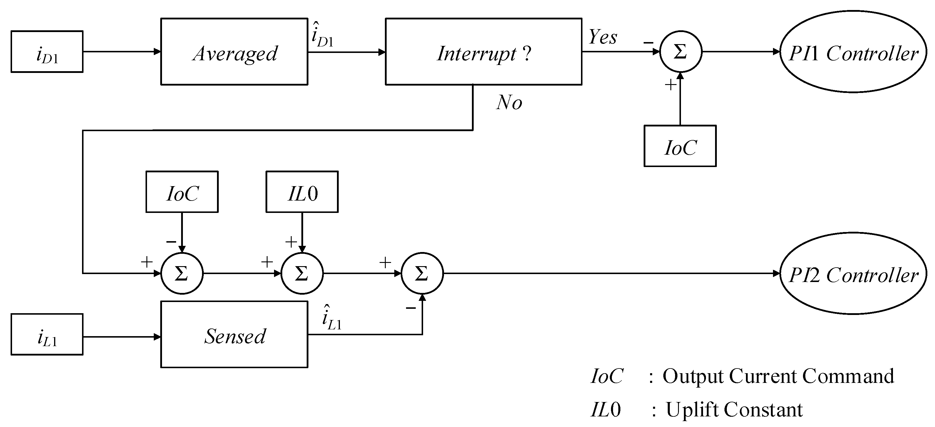
4.3. Main Program Control Function

Figure 24 shows a block diagram of the main program control function. In this figure, the diode current iD1 is averaged over half of a utility cycle to obtain i ^ D 1 . Subsequently, if the interrupt is activated, then the output current command IoC minus this average value is sent to the first proportional–integral (PI) controller. On the other hand, i ^ D 1 minus the output current command IoC plus the uplift constant IL0 is used to create the current command of the inductor L1, and then the sensed inductor current i ^ L 1 minus this command is sent to the second PI controller. In this paper, the digital control program is written according to Figure 24. The duty cycle of the switch S1 can be fixed for half of a utility cycle generated by the interrupt based on the triggering signal vtrig, as shown in Figure 23, and the output average current and the active low-frequency current ripple suppression unit can be controlled, respectively.

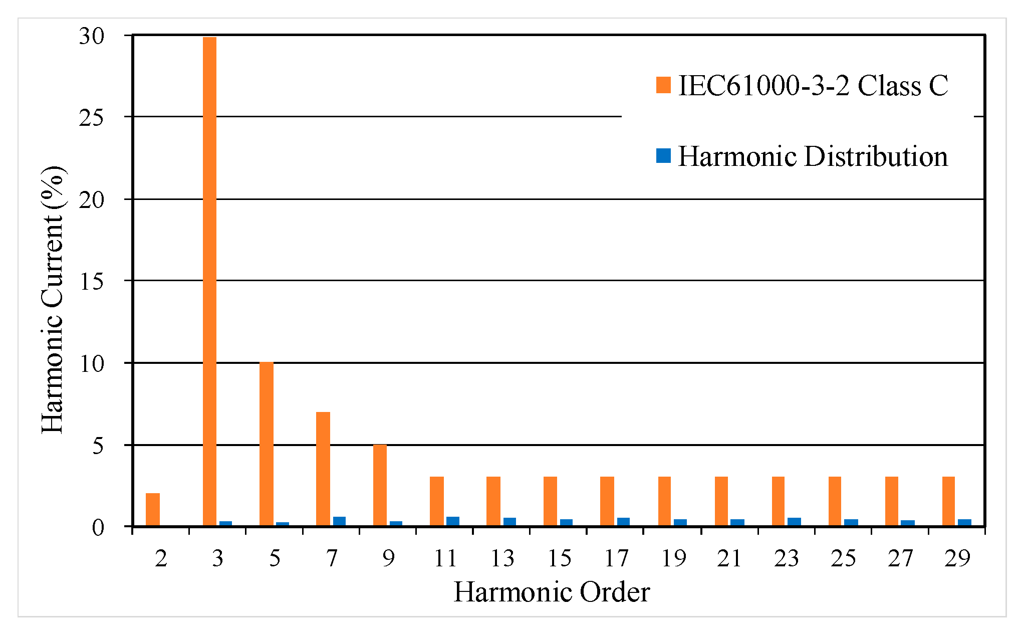
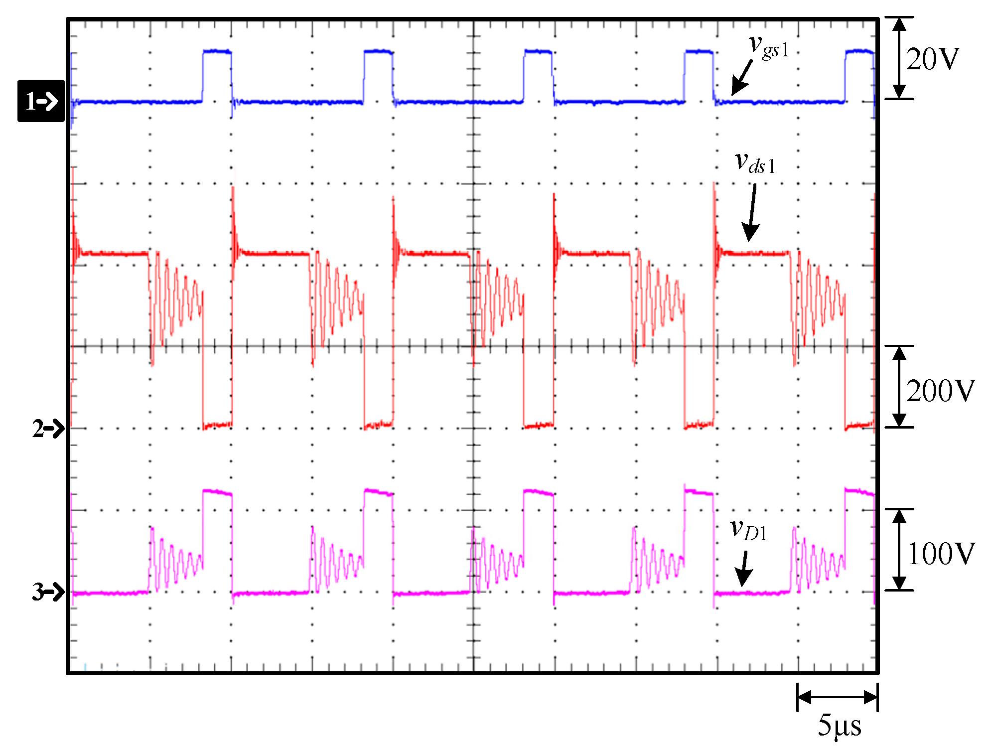
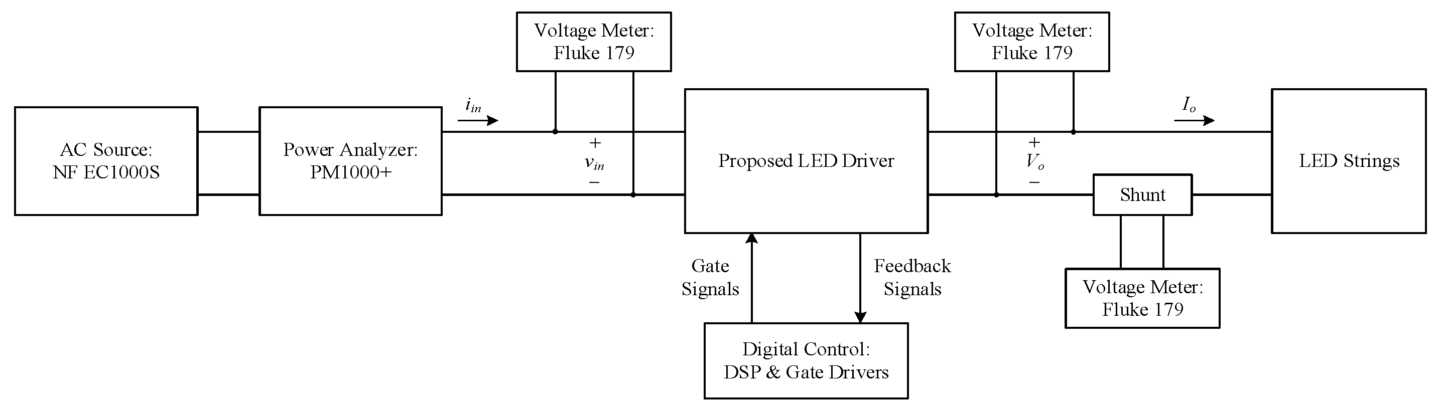
5. Experimental Results

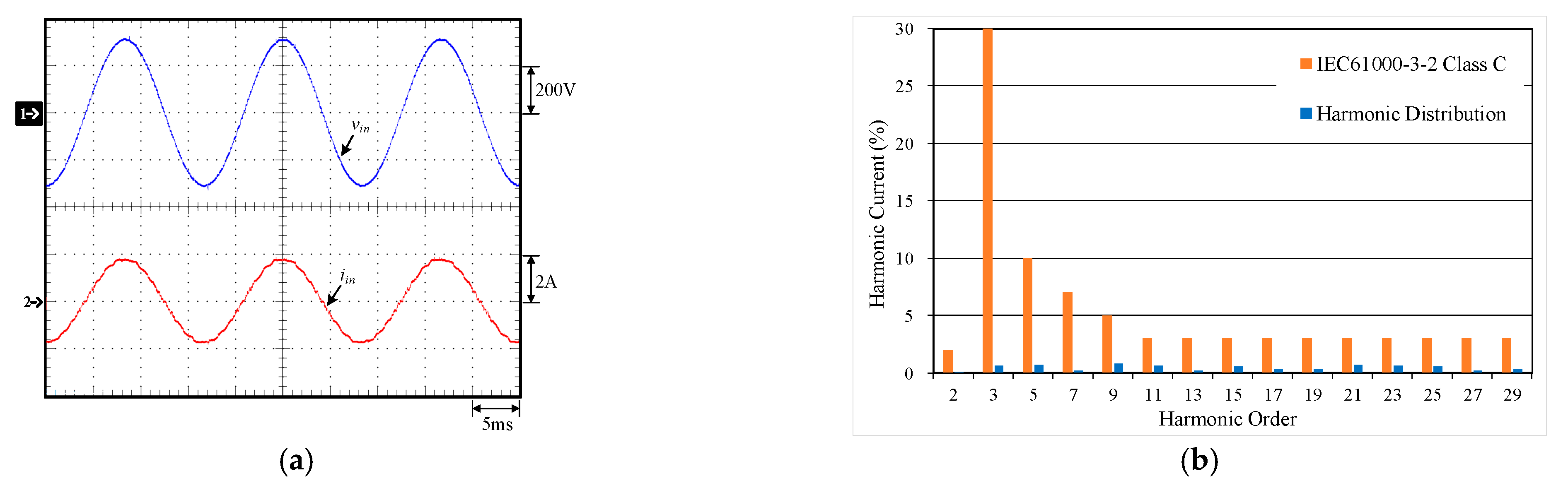
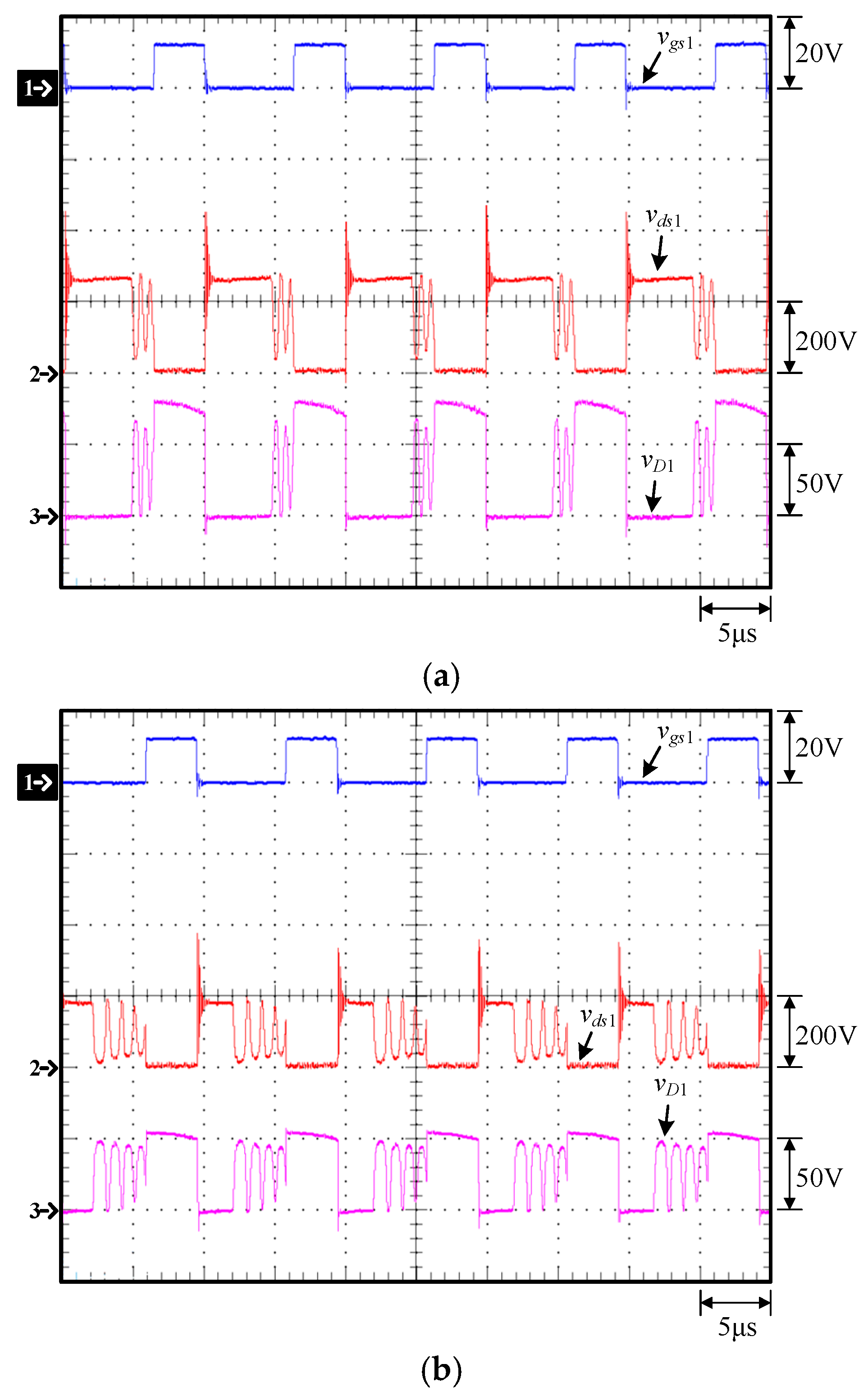
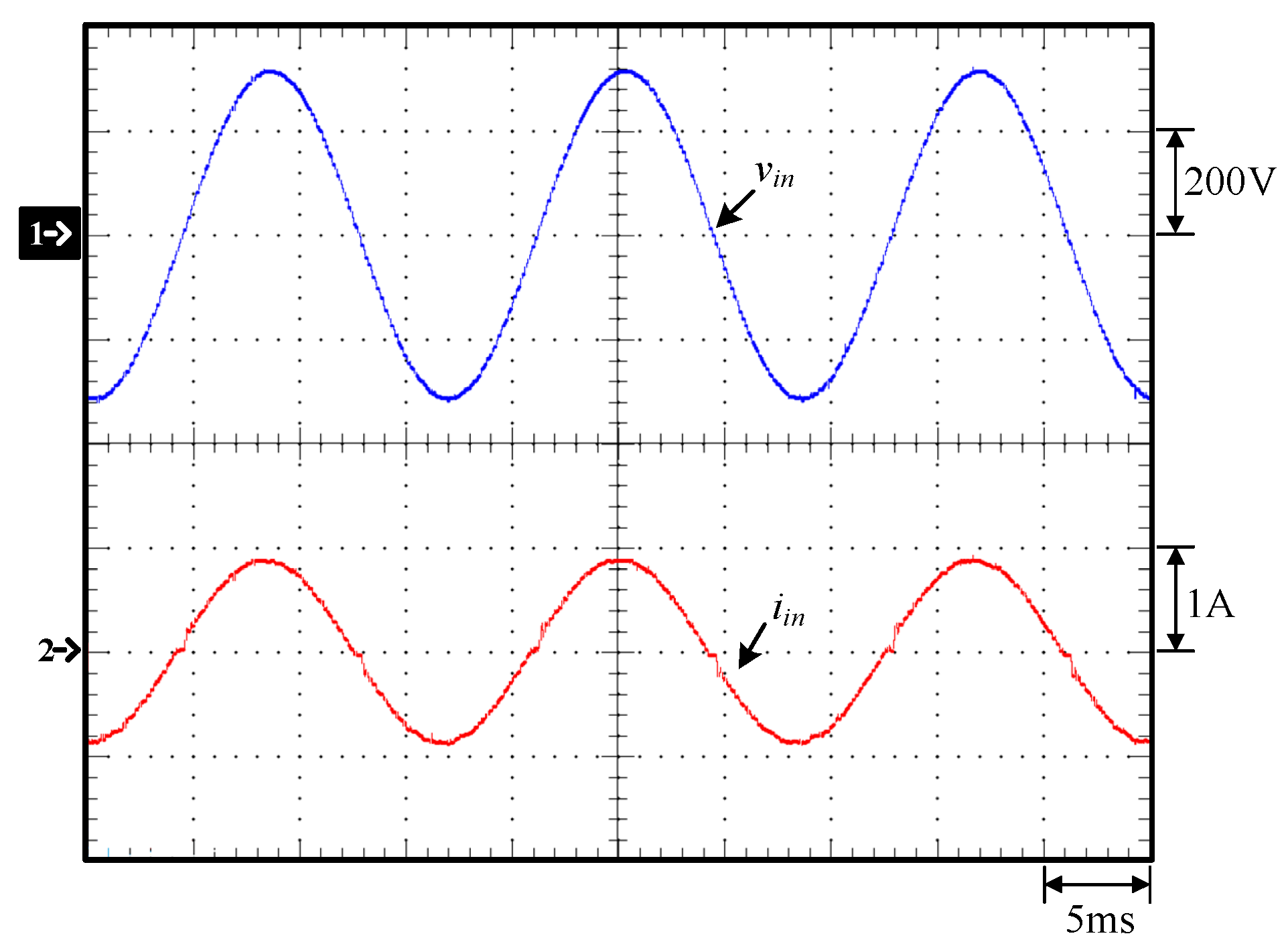
5.1. Input Voltage of 110 V at Rated Load

Figure 25a shows the input voltage vin and input current iin. Figure 25b provides a comparison of the input current harmonic distribution with IEC61000-3-2 Class C. The values are in accordance with Class C requirements. Figure 26a shows the gate driving signal vgs1 for the switch S1, the voltage vds1 across the switch S1, and the voltage vD1 across the diode D1 at the input voltage near the peak. Figure 26b shows the gate driving signal vgs1 for the switch S1, the voltage vds1 across the switch S1, and the voltage vD1 across the diode D1 at the input voltage near the zero-crossing point. At rated load, Figure 26a,b show that the duty cycle of the switch S1 is fixed for half of a utility cycle; Figure 27a shows the current io_flyback in the output of the flyback converter, the inductor current iL1 in the inductor L1, the output current io, and the voltage vC1 across the capacitor C1; Figure 27b shows the output current ripple Δio. However, if the control force is reduced, the low-frequency ripple suppression effect will be reduced. Therefore, in this paper, the control force is set to a high value to obtain a better low-frequency ripple suppression effect despite the oscillation. When the inductor current iL1 changes from a positive to negative half cycle, it can be seen from Figure 27a,b that the output current variation of Δio decreases considerably, whereas when the inductor current iL1 changes from a negative to positive half cycle, the output current variation of Δio decreases by less, and then the inductor current iL1 appears as a small flat area close to 0A, that is, the inductor current iL1 cannot be controlled by the digital controller. In contrast, when the inductor current iL1 changes from a positive to a negative half cycle, the reason for the larger sag in the output current variation of Δio is that the current iL1 is smaller and more easily disturbed.

5.2. Input Voltage of 220 V at Rated Load

Figure 28 shows the input voltage vin and input current iin. Figure 29 provides a comparison of the input current harmonic distribution with IEC61000-3-2 Class C. The values are in accordance with Class C requirements. Figure 30 shows the gate driving signal vgs1 for the switch S1, the voltage vds1 across the switch S1, and the voltage vD1 across the diode D1 at the input voltage near the peak. Figure 31 shows the gate driving signal vgs1 for the switch S1, the voltage vds1 across the switch S1, and the voltage vD1 across the diode D1 at the input voltage near the zero-crossing point. At rated load, as shown in Figure 30 and Figure 31, the duty cycle of the switch S1 is fixed for half a utility cycle; Figure 32 shows the current io_flyback in the output of the flyback converter, the inductor current iL1 in the inductor L1, the output current io, and the voltage vC1 across the capacitor C1. Figure 33 shows the output current ripple Δio. However, if the control force is reduced, the low-frequency ripple suppression effect will be reduced. Therefore, in this paper, the control force is set to a high value to obtain a better low-frequency ripple suppression effect despite the oscillation. When the inductor current iL1 changes from a positive to negative half cycle, from Figure 32 and Figure 33, it can be seen that the output current variation of Δio decreases considerably, whereas when the inductor current iL1 changes from a negative to a positive half cycle, the output current variation of Δio decreases by less, and then the inductor current iL1 appears as a small flat area close to 0 A, that is, the inductor current iL1 cannot be controlled by the digital controller. In contrast, when the inductor current iL1 changes from a positive to negative half cycle, the reason for the larger sag in the output current variation of Δio is that the sensed current iL1 is smaller and more easily disturbed. Compared to the results measured under 110 V input voltage, the duty cycle of the switch S1 that is fixed for half a utility cycle is relatively small, and the ring phenomenon is relatively serious.

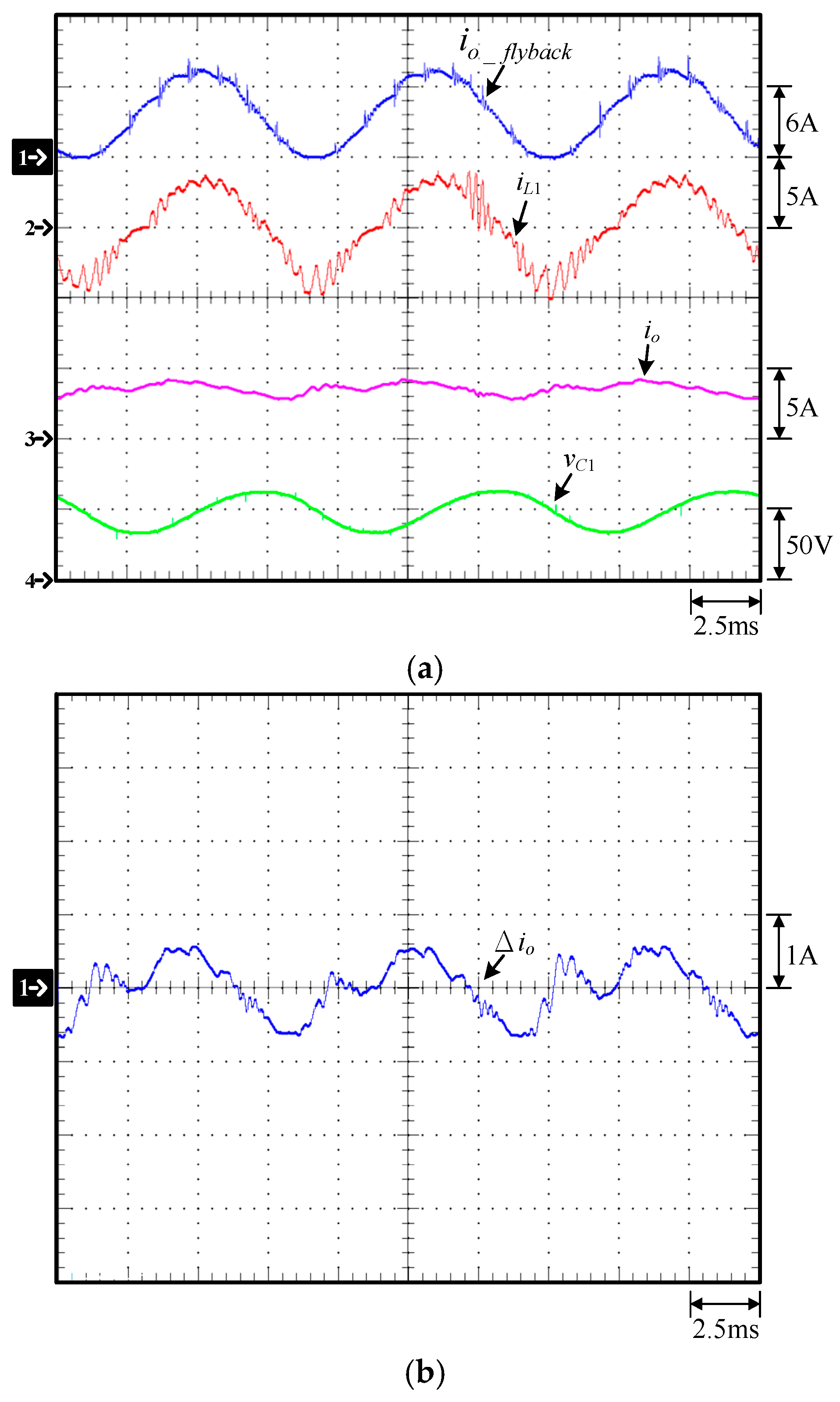
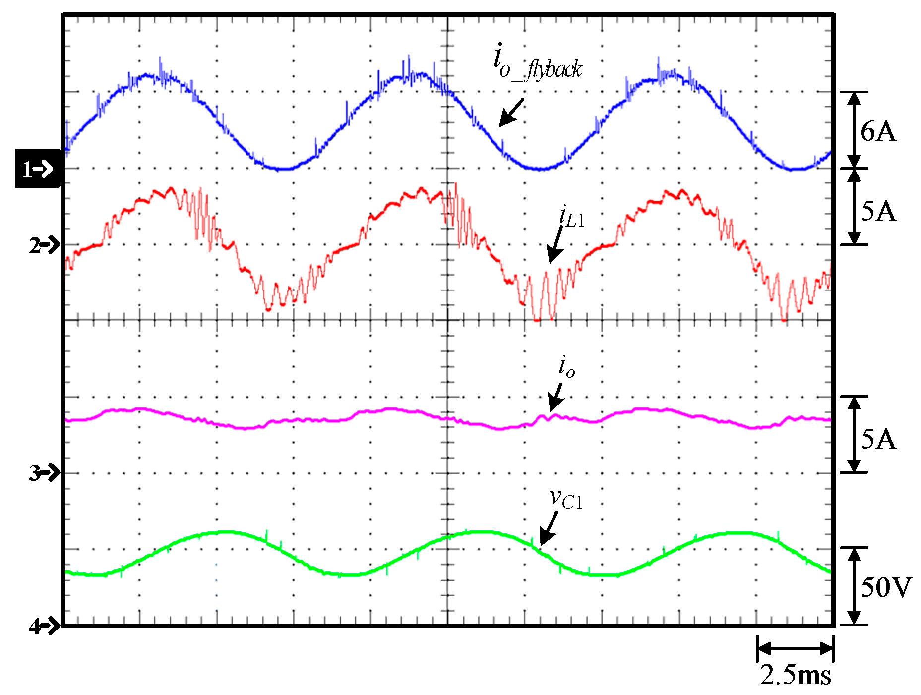
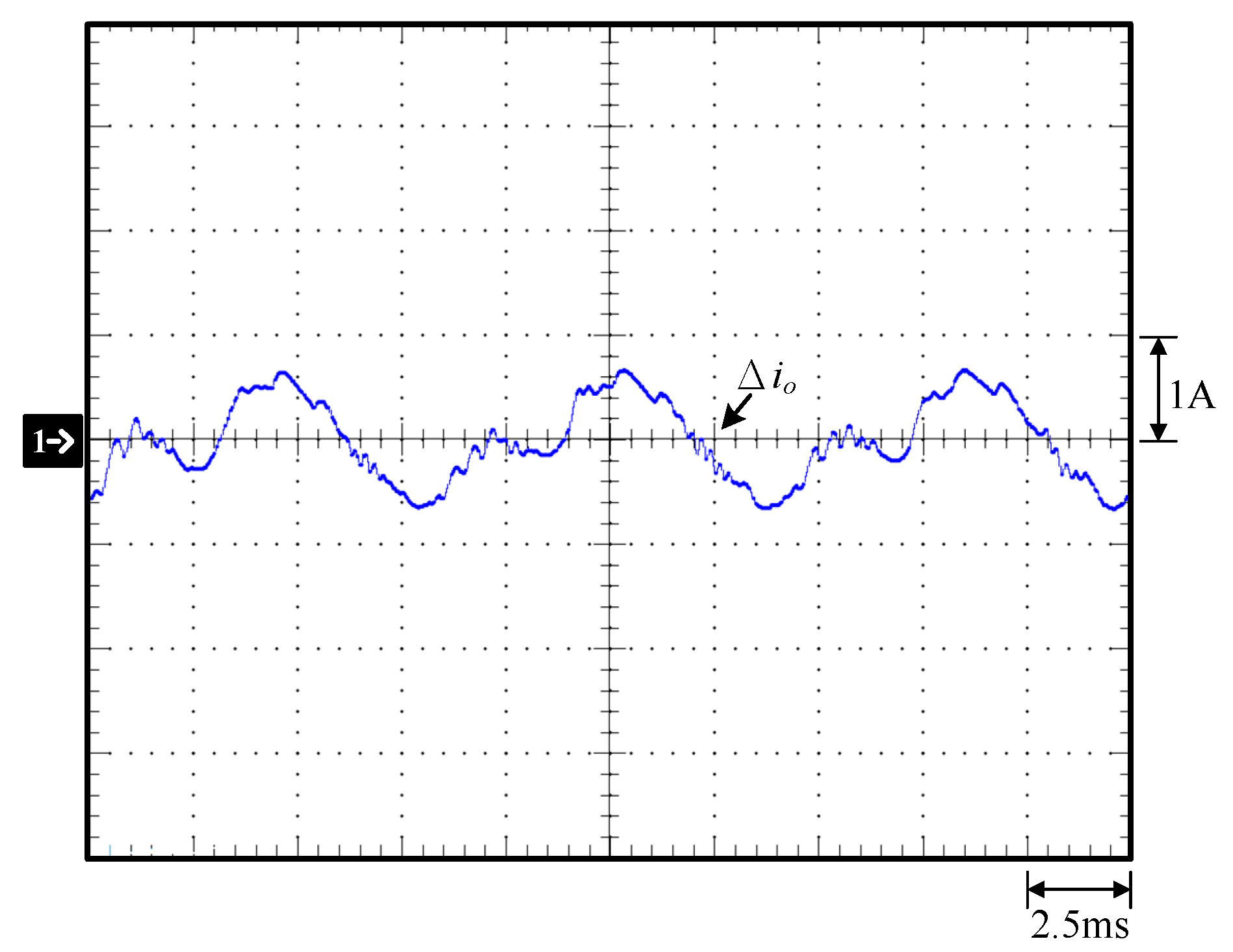
5.3. Output: Current Ripple Suppression

Table 4 and Table 5 show the output current ripple amplitude and output current ripple suppression percentage, respectively. They also show that the effectiveness of the proposed ALFCRSU has been verified.

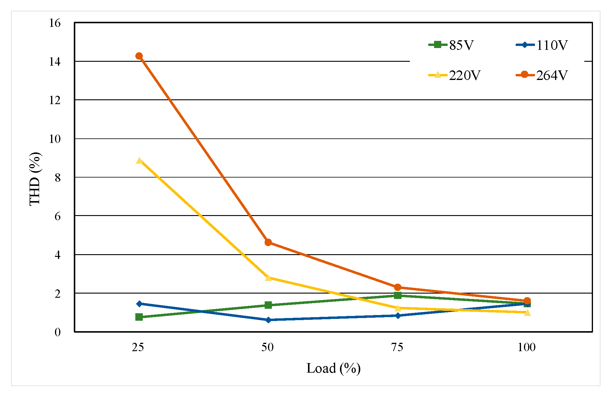
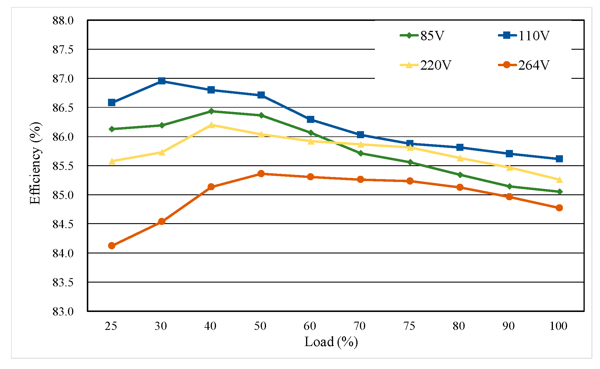
5.4. Other Associated Measurements

The total harmonic distortion, power factor, and efficiency of the proposed circuit are measured for different output currents at four different input voltages. The measurement method is shown in Figure 34. First, a power analyzer (PM1000+) is used to measure the input current, total harmonic distortion (THD), and power factor (PF). Then, a digital meter (Fluke 179, manufactured by FLUKE Co., Everett, WA, USA) is used to measure the input voltage, output voltage, and the voltage across the current shunt to obtain the output current, from which the input power and output power can be obtained. Finally, the resulting input and output power are used to calculate the corresponding efficiency. Figure 35 shows the curve of total harmonic distortion versus load under different input voltages. Figure 36 shows the curve of power factor versus load at different input voltages. Figure 37 shows the curve of efficiency versus load under different input voltages.
From Figure 35, it can be seen that the low-voltage input can maintain low total harmonic distortion under any load condition; the high-voltage input can also maintain low total harmonic distortion above heavy load, but below half load, the total harmonic distortion increases due to increasing zero-crossing distortion. From Figure 36, under the input voltages of 85 V and 110 V, it can be seen that almost no zero-crossing distortion occurs for all load conditions, and the phase difference between input voltage and input current is very small, so the high power factor can be maintained. When the output power is fixed, comparing the measured results of the 110 V input with those of the 220 V input, the capacitive current of the 220 V input is the same as that of the 110 V input, and the input current of the 220 V input is lower than that of the 110 V input. Therefore, the power factor of the 220 V input is lower than that of the 110 V input. To summarize, the proposed circuit has a high power factor. As can be seen from Figure 37, the efficiency of the LED driver can be maintained at 84% or higher, with a maximum efficiency of 86.95% at the 110 V input voltage and 30% load. This flat area can be eliminated by changing the parameters of the digital controller. This is because the capacitor voltage vC1 will not decrease to near the average output voltage Vo, and this means that more energy must be supplied to the capacitor C1, and hence, the efficiency will be reduced. Accordingly, the flat area with some inductor current (iL1) is adopted herein to obtain better efficiency.

6. Conclusions

This paper applies a control method of a fixed duty cycle in each half of the utility cycle to a single-stage AC/DC converter, built by using a flyback converter, and this has the advantages of a high power factor and simple control. Furthermore, an active low-frequency ripple suppression unit is employed to reduce the output low-frequency ripple and thereby decrease the flicker of the LED load. The proposed method makes sure that the input current can be in phase with the universal input voltage, thus achieving a high power factor without utilizing feedforward control. Furthermore, not only can the time of the zero point of the utility voltage be attained on the secondary side, so that the duty cycle can be updated at the time of the zero point of the utility voltage, but also the simple auxiliary circuit is connected parallel to the output side to absorb the excess output current of the flyback converter or to release the current to the load to make up for the shortage of the output current of the flyback converter. As a result, the low-frequency ripple of the output current can be suppressed easily. In the future, the number of LED strings will increase along with the soft switching considered in this study and applied to street lighting.

Author Contributions

Conceptualization, K.-I.H. and C.-T.L.; methodology, C.-T.L.; software, J.-J.S.; validation, C.-T.L., K.-I.H. and J.-J.S.; formal analysis, C.-T.L.; investigation, J.-J.S.; resources, C.-T.L.; data curation, J.-J.S.; writing—original draft preparation, K.-I.H.; writing—review and editing, K.-I.H.; visualization, J.-J.S.; supervision, K.-I.H.; project administration, K.-I.H.; funding acquisition, J.-J.S. All authors have read and agreed to the published version of the manuscript.

Funding

This research was funded by the Ministry of Science and Technology, Taiwan, under Grant Number NSTC 112-2221-E-035-010.

Data Availability Statement

Data are contained within the article.

Conflicts of Interest

The authors declare no conflict of interest.

References

  1. Faizan, M.; Bi, J.; Liu, M.; Wang, L.; Stempitsky, V.; Yousaf, M.Z. Long life power factor corrected LED driver with capacitive energy mechanism for street light applications. Sustainability 2023, 15, 3991. [Google Scholar] [CrossRef]
  2. Ahn, H.-A.; Seong-Kwan, H.; Oh-Kyong, K. A highly accurate current led lamp driver with removal of low-frequency flicker using average current control method. IEEE Trans. Power Electron. 2018, 33, 8741–8753. [Google Scholar] [CrossRef]
  3. Ghazali, M.; Adib, E. High performance single stage power factor correction circuit. IET Power Electron. 2022, 15, 145–154. [Google Scholar] [CrossRef]
  4. Li, Z.; Zhang, Y.; Liu, J.; Wang, Z.; Wu, Y.; Li, N.; Si, J. A second-harmonic suppression method based on differentiated-capacitance design for input-parallel output-series DAB fed single-phase VSI. IEEE Trans. Power Electron. 2022, 37, 11592–11606. [Google Scholar] [CrossRef]
  5. Mohsen, M.J.E.; Reza, F.M.F.; Beiranvand, B.R. CCM operation of a single-stage boost-flyback converter with active-clamp for LED driver applications. In Proceedings of the 11th Power Electronics, Drive Systems, and Technologies Conference (PEDSTC), Tehran, Iran, 1–4 February 2020. [Google Scholar]
  6. Satit, M.; Chainarin, E.; Kamon, J.; Phatiphat, T.; Kohji, H.; Marian, K.K. A single-stage LED driver based on ZCDS class-E current-driven rectifier as a PFC for street-lighting applications. IEEE Trans. Power Electron. 2018, 33, 8710–8727. [Google Scholar]
  7. Kim, H.-C.; Choi, M.C.; Kim, S.; Jeong, D.-K. An AC-DC LED driver with a two-parallel inverted buck topology for reducing the light flicker in lighting applications to low-risk levels. IEEE Trans. Power Electron. 2017, 32, 3879–3891. [Google Scholar] [CrossRef]
  8. Lee, S.-W.; Do, H.-L. A single-switch AC-DC LED driver based on a boost-flyback PFC converter with lossless snubber. IEEE Trans. Power Electron. 2017, 32, 1375–1384. [Google Scholar] [CrossRef]
  9. Singh, A.K.; Mishra, A.K.; Gupta, K.K.; Kim, T. Comprehensive review of nonisolated bridgeless power factor. IET Circuits Devices Syst. 2021, 15, 197–208. [Google Scholar] [CrossRef]
  10. Peng, F.; Samuel, W.; Yang, C.; Yan-Fei, L.; Paresh, C.S. A multiplexing ripple cancellation LED driver with true single-stage power comversion and flicker-free operation. IEEE Trans. Power Electron. 2019, 34, 10105–10120. [Google Scholar]
  11. Yang, P.; Cao, J.; Shang, Z.; Cai, Y.; Xu, J. Double-line frequency ripple suppression of a quasi-single stage AC-DC converter. IEEE Trans. Circuits Syst. II Express Briefs 2020, 67, 2074–2078. [Google Scholar] [CrossRef]
  12. Valipour, H.; Rezazadeh, G.; Zolghadri, M.R. Flicker-free electrolytic capacitor-less universal input offline LED driver with PFC. IEEE Trans. Power Electron. 2016, 31, 6553–6561. [Google Scholar] [CrossRef]
  13. Qiu, Y.; Wang, L.; Wang, H.; Liu, Y.-F.; Sen, P.C. Bipolar ripple cancellation method to achieve single-stage electrolytic-capacitor-less high-power LED driver. IEEE J. Emering Sel. Top. Power Electron. 2015, 3, 698–713. [Google Scholar]
  14. Hao, W.; Siu-Chung, W.; Chi, K.T. A PFC single-coupled-inductor multiple-output LED driver without electrolytic capacitor. IEEE Trans. Power Electron. 2019, 34, 1709–1725. [Google Scholar]
  15. Hao, W.; Siu-Chung, W.; Chi, K.T. A more efficient PFC sigle-couple-inductor multiple-output electrolytic capacitor-less LED driver with energy-flow-path optimization. IEEE Trans. Power Electron. 2019, 34, 9052–9066. [Google Scholar]
Figure 1. Main power stage built by FC and ALFCRSU with point A between D1 and Co and point B between L1 and Ro.
Energies 17 00183 g001
Figure 2. The main power stage built by FC and ALFCRSU with point A between D1 and Co and point B between L1 and Ro, with symbols indicated.
Energies 17 00183 g002
Figure 3. Illustrated waveforms relevant to the driver’s operating states.
Energies 17 00183 g003
Figure 4. Equivalent circuit of the proposed topology in state I.
Energies 17 00183 g004
Figure 5. Illustrated waveforms of the FC in state I.
Energies 17 00183 g005
Figure 6. Current flow of the FC in mode 1 in state I, with red dashed lines indicated.
Energies 17 00183 g006
Figure 7. Current flow of the FC in mode 2 in state I, with red dashed lines indicated.
Energies 17 00183 g007
Figure 8. Current flow of the FC in mode 3 in state I, with red dashed lines indicated.
Energies 17 00183 g008
Figure 9. Key waveforms of the ALFCRSU in State I.
Energies 17 00183 g009
Figure 10. Current flow of the ALFCRSU in mode 1 in State I, with red dashed lines indicated.
Energies 17 00183 g010
Figure 11. Current flow of the ALFCRSU in mode 2 in state I, with red dashed lines indicated.
Energies 17 00183 g011
Figure 12. Equivalent circuit of the proposed topology in state II.
Energies 17 00183 g012
Figure 13. Key waveforms of the FC in state II.
Energies 17 00183 g013
Figure 14. Current flow of the FC in mode 1 in state II, with red dashed lines indicated.
Energies 17 00183 g014
Figure 15. Current flow of the FC in mode 2 in State II, with red dashed lines indicated.
Energies 17 00183 g015
Figure 16. Current flow of the FC in mode 3 in State II, with red dashed lines indicated.
Energies 17 00183 g016
Figure 17. Illustrated waveforms of the ALFCRSU in State II.
Energies 17 00183 g017
Figure 18. Current flow of the ALFCRSU in mode 1 in State II, with red dashed lines indicated.
Energies 17 00183 g018
Figure 19. Current flow of the ALFCRSU in mode 2 in State II, with red dashed lines indicated.
Energies 17 00183 g019
Figure 20. System configuration. (a) Block diagram of system; (b) Photo of the experimental setup: (1) top side; (2) bottom side.
Energies 17 00183 g020
Figure 21. Operation of the input voltage waveform restoration circuit: (a) S1 is on and Da is on; (b) S1 is off but Da is off.
Energies 17 00183 g021
Figure 22. Zero-voltage detection circuit.
Energies 17 00183 g022
Figure 23. Waveforms relevant to the input voltage waveform restoration circuit are vCa (upper) and vtrig (lower).
Energies 17 00183 g023
Figure 24. Block diagram of the main program control function.
Energies 17 00183 g024
Figure 25. Measured waveforms at rated load under 110 V input voltage. (a) (1) vin; (2) iin; (b) Harmonic distribution of input current.
Energies 17 00183 g025
Figure 26. Measured waveforms at the rated load with the input voltage. (a) Near the peak under 110 V input voltage: (1) vgs1; (2) vds1; (3) vD1; (b) Near the zero-crossing point under 110 V input voltage: (1) vgs1; (2) vds1; (3) vD1.
Energies 17 00183 g026
Figure 27. Measured waveforms at rated load under 110 V input voltage. (a) (1) io_flyback; (2) iL1; (3) io; (4) vC1; (b) (1) Δio.
Energies 17 00183 g027
Figure 28. Measured waveforms at rated load under 220 V input voltage: (1) vin; (2) iin.
Energies 17 00183 g028
Figure 29. Harmonic distribution of the input current at the rated load under 110 V input voltage.
Energies 17 00183 g029
Figure 30. Measured waveforms at rated load with the input voltage near the peak under 220 V input voltage: (1) vgs1; (2) vds1; (3) vD1.
Energies 17 00183 g030
Figure 31. Measured waveforms at rated load with the input voltage near the zero-crossing point under 220 V input voltage: (1) vgs1; (2) vds1; (3) vD1.
Energies 17 00183 g031
Figure 32. Measured waveforms at rated load under 220 V input voltage: (1) io_flyback; (2) iL1; (3) io; (4) vC1.
Energies 17 00183 g032
Figure 33. Measured waveforms at rated load under 110 V input voltage: (1) Δio.
Energies 17 00183 g033
Figure 34. Block diagram of efficiency measurement.
Energies 17 00183 g034
Figure 35. Curve of total harmonic distortion versus load.
Energies 17 00183 g035
Figure 36. Curve of PF versus load.
Energies 17 00183 g036
Figure 37. Curve of efficiency versus load.
Energies 17 00183 g037
Table 1. LED specifications.
SpecificationsValues
Forward Voltage (VF)2.95V~3.85 V
DC Operating Current (IF,max)400 mA
Pulsed Forward Current500 mA
Junction Temperature125 °C
Operating Temperature−40 °C~85 °C
Typical Light Flux Output100 lm @ 350 mA
Table 2. LED driver specifications.
SpecificationsValues
Normal Input Voltage (Vin_nor)110 Vrms
Maximum Input Voltage (Vin_max)264 Vrms
Minimum Input Voltage (Vin_min)85 Vrms
Line Frequency (fline)60 Hz
Rated Output Voltage (Vo_rated)34.5 V (=3.45 V × 10)
Rated Output Current (Io_rated)350 mA × 10 = 3.5 A
System Operation ModeDCM
Switching Frequency (fs1) for FC100 kHz
Switching Frequency (fs2) for ALFCRSU200 kHz
LED SpecificationsVF = 3.45 V, IF = 0.35 A (Rated Load)
VF = 2.9 V, IF = 87.5 mA (Light Load)
Number of LEDs on the LED String10
Table 3. A summary of the component specifications of the proposed circuit.
ComponentsSpecifications
BD1T8KB60
S1SPA20N60C
S2, S3SUP85N10
D1SBR30300CT
Cf10.1 μF Film Capacitor
Cf20.47 μF Film Capacitor
C1220 μF Electrolytic Capacitor
Co141 μF Multi-Layer Ceramic Capacitor
470 μF Electrolytic Capacitor
T1Core: LP3320, Lm = 61.22 μH, n = 3.5
L1Core: T94-52 64 μH
LfCore: T106-45, 800 μH
Isolated Gate DriversTLP250H
Table 4. Output current ripple amplitude.
Output CurrentSuppressionNo Suppression
110 V220 V110 V220 V
0.88 A (25%)1.73 A1.75 A0.73 A0.8 A
1.75 A (50%)3.5 A3.55 A0.83 A1.01 A
3.5 A (100%)6.9 A6.8 A1.2 A1.33 A
Table 5. Output current ripple suppression percentage.
Output Current110 V220 V
0.88 A (25% Load)57.8%54.3%
1.75 A (50% Load)78.29%71.55%
3.5 A (100% Load)82.61%80.44%
Disclaimer/Publisher’s Note: The statements, opinions and data contained in all publications are solely those of the individual author(s) and contributor(s) and not of MDPI and/or the editor(s). MDPI and/or the editor(s) disclaim responsibility for any injury to people or property resulting from any ideas, methods, instructions or products referred to in the content.

