Article

Research on Voltage Compensation Methods and Optimization Algorithm for Insulated Core Transformer High-Voltage Power Supply

1
14th Research Institute, China Electronics Technology Group Corporation, Nanjing 210013, China
2
NARI Group Corporation (State Grid Electric Power Research Institute), Nanjing 211106, China
3
State Key Laboratory of Advanced Electromagnetic Engineering and Technology, Huazhong University of Science and Technology, Wuhan 430074, China
*
Author to whom correspondence should be addressed.
Energies 2024, 17(3), 547; https://doi.org/10.3390/en17030547
Submission received: 23 December 2023 / Revised: 15 January 2024 / Accepted: 21 January 2024 / Published: 23 January 2024

Abstract

:
The insulated core transformer (ICT) power supply is widely employed in electron beam accelerators (EBAs) due to its high power, heightened efficiency, and stable operation. However, the segmented-core structure of the ICT power supply increases magnetic leakage, which leads to it adversely affecting the consistency of the output voltages in the rectifier stages. Currently, numerous studies focus on stage voltage compensation, including turns compensation, capacitor compensation, dummy primary winding compensation, and full-parameter compensation. This paper presents a unified simulation model and an improved gradient-based genetic algorithm, which can also optimize the parameters of the four compensation methods. Based on this, the performance of the power supply using the four compensation methods under different ICT energy levels and power supply requirements is studied, and the selection suggestions are given. This work fills the gap in the performance comparison and application research of various compensation methods.

1. Introduction

Electron beams are widely applied in material modification [1], environmental protections [2,3], electron microscopy [4,5], and so on [6]. The ICT power supply, renowned for its high efficiency (>85%), robust power output, and reliability, has emerged as a preferred option for supplying energy to the electron beam [7,8].
The general structure of a three-phase ICT (insulated core transformer), as depicted in Figure 1, comprises two yokes, three magnetic core columns, one set of primary wingdings (p), and multiple sets of secondary windings (1#, 2# … s# ... N#) [9]. With dummy primary winding (DPW) compensation, a set of dummy primary wingdings (d) of the same size as the primary wingdings are added to the top of the core. The primary cores and primary wingdings are situated in the lowest layer. The secondary cores, secondary wingdings, and the rectifier circuits comprise the rectifier disk. Lastly, the N stages are stacked from bottom to top. By connecting the DC outputs of the stages in series, the power supply can achieve a high output voltage, which is then used to supply power to the electron accelerator. Compared to conventional transformers, the ICT exhibits a significant distinction: its magnetic cores are segmented by insulating sheets with a high dielectric capability. This segmentation leads to a considerable amount of magnetic flux leakage, resulting in two unfavorable consequences: (1) a reduction in the induced voltage of the secondary windings; and (2) an increase in leakage inductance and output impedance [10]. The voltage doubling rectifier circuit converts the three-phase AC output from the secondary windings into DC. Due to the withstand voltage limitation of the rectifier circuit and insulation materials [11], the stage output voltage must not exceed the rated value. Significant voltage fluctuations between stages can result in underutilization of the rectifier disks, leading to a decrease in the overall output voltage.
To reduce the stage output voltage nonuniformity, several methods have been suggested by researchers. Van de Graaff proposes the I-shaped magnetic core [11,12] to reduce magnetic flux leakage. However, this approach entails complex manufacturing processes and high costs [13]. The turns compensation method increases the turns of the secondary windings according to the magnetic flux leakage distribution of each stage [13]. The capacitor compensation method [14,15] employs parallel capacitors across the secondary windings, and the additional excitation flux generated by the capacitive current is used to compensate the flux leakage. However, when the number of ICT layers is large, these two methods are difficult to ensure the high stage voltage consistency from load to full load. The full-parameter compensation method, proposed by the Huazhong University of Science and Technology (HUST) [16], integrates turns compensation and capacitor compensation to achieve a high voltage consistency. Additionally, the DPW compensation adds a set of dummy primary wingdings to induce additional flux to compensate for the magnetic leakage.
With the exception of the I-shaped magnetic core method, the other four compensation methods are commonly utilized in engineering due to their ease of fabrication using regular cores and a simpler adjustment of winding turns or compensation capacitance values. However, there is a lack of analysis and comparison of their performance and application range. On the other hand, for the parameter optimization of these compensation methods, researchers have proposed the artificial iterative method (IM) [16], genetic algorithm (GA) [17], particle swarm optimization (PSO) [8,18], and other methods. However, these methods are difficult to satisfy the optimization of all compensation methods simultaneously. Therefore, this paper innovatively proposes a unified calculation model and an improved gradient-based genetic algorithm, which can be applied to the four compensation methods. At the same time, the calculation of the number of turns or the compensation capacitance value for the traditional turns compensation, traditional capacitor compensation, and dummy primary compensation methods is improved from a formula to an iterative algorithm optimization. Furthermore, based on the unified simulation model and algorithm, the performance of different compensation methods for different voltage levels of ICT applications was compared. Finally, through comparison, this paper gives the use scenarios and selection recommendations of different compensation methods, which fills the research gap and contributes to the design optimization of an ICT.

2. Compensation Methods

The following is a brief review of the four compensation methods.

2.1. Turns Compensation Method

The traditional turns compensation method is based on the law that the induced voltage of the secondary winding is proportional to the number of turns. If the mutual inductances between the primary winding and each secondary winding Mps are equal, each secondary winding can output the same no-load voltage U s n . According to this principle, secondary winding turns ns can be calculated by (1) [16].
n s = U s n U p n L p ( 1 ) M p s ( 1 ) n p k
U p n is the input voltage of the primary winding under no-load conditions, whose unit is V. The superscript “n” stands for the no-load case. Mps(1) = Mps/(ns*np) is the single-turn mutual inductance [19] from the primary winding to the s# secondary winding, whose units are H; Lp(1) = Lp/np2 is the single-turn self-inductance of the primary winding, whose units are H. The mutual inductance matrix of single-turn wingdings on the same phase M(1) can fully describe the terminal voltage–current properties of the transformer. Its value can be obtained via finite-element method (FEM) simulation or be measured [20]. The k is the unified compensation coefficient and used to compensate the voltage drop of rectifier diodes, and its value is 1.1~1.4.
The traditional turns compensation method ensures the second winding output voltages under no-load conditions U s n are equal. However, when the power supply is loaded, the voltages of the secondary windings located far from the primary winding decrease to a greater extent. Therefore, it is difficult to keep the output voltages consistent [16]. Different from this, the improved turns compensation method (ITC) takes the ns calculated by Equation (1) as the initial value, while the voltage nonuniformity at no-load and full-load conditions and the load adjustment rate are taken as the optimization objectives, and finally, the optimal secondary winding turns are solved by the optimization algorithm. This method can improve the load-carrying capacity of the power supply.

2.2. Dummy Primary Winding Compensation Method (DPWC)

The dummy primary winding (DPW) technique is employed in the accelerator from the manufacturer Wosik. The DWP is connected in parallel with a resonant capacitor Cd. With an aim to curtail expenses, the DPWs are usually exactly the same as the primary windings. In order to generate the same magnetic flux as the real primary winding, the voltage U d n of the DWP at no load is designed to be equal to the input voltage U p n of the primary winding. The current of the DWP also approximates that of the primary winding. Hence, neglecting the winding’s resistance, the value of Cd should be Equation (2), whose unit is F.
C d = 1 / ( ω 2 n p 2 ( L ( 1 ) p + M ( 1 ) p d ) )
ω is the angular frequency of 100π rad/s.
In this case, the magnetic flux of the s# secondary winding is affected by both the primary winding and the DWP, so its turns ns calculation should be Equation (3).
n s = U s U p L p ( 1 ) + M p d ( 1 ) M p s ( 1 ) + M d s ( 1 ) n p k
Just like the traditional turns compensation, when the power supply is loaded, the output voltages of the secondary windings in the middle section will decrease more. Similarly, ns (s = 1…N) can be set as the variables for optimization in the DWPC, and the result of Equation (3) can be used as the initial value for optimization.

2.3. Capacitor Compensation Method

The traditional capacitor compensation method was applied in the Cross ICT of KSI [21] and the planar ICT [13] of the Chinese Academy of Sciences. The capacitive current of the compensation capacitor induces magnetic flux to compensate for the magnetic flux drop by the insulation gap. Based on this compensation principle, Cs is (4) [21], whose unit is F.
C s = l g / n s 2 ω 2 μ 0 S c o r e
lg is the height of the insulation gap, whose unit is m. Score is the cross-sectional area of the magnetic core, whose unit is m2. μ0 is the permeability of the insulation sheet. The traditional capacitor compensation also experiences significant fluctuations in stage voltage uniformity from a no-load to a full-load condition [16]. Recognizing the ease of adjusting capacitance Cs by combining capacitors with varying parameter specifications, an improved capacitor compensation method (ICC) is introduced. Cs (s = 1…N) are set as the optimization variables, achieving optimal voltage uniformity through an optimization algorithm.

2.4. Full-Parameter Compensation Method

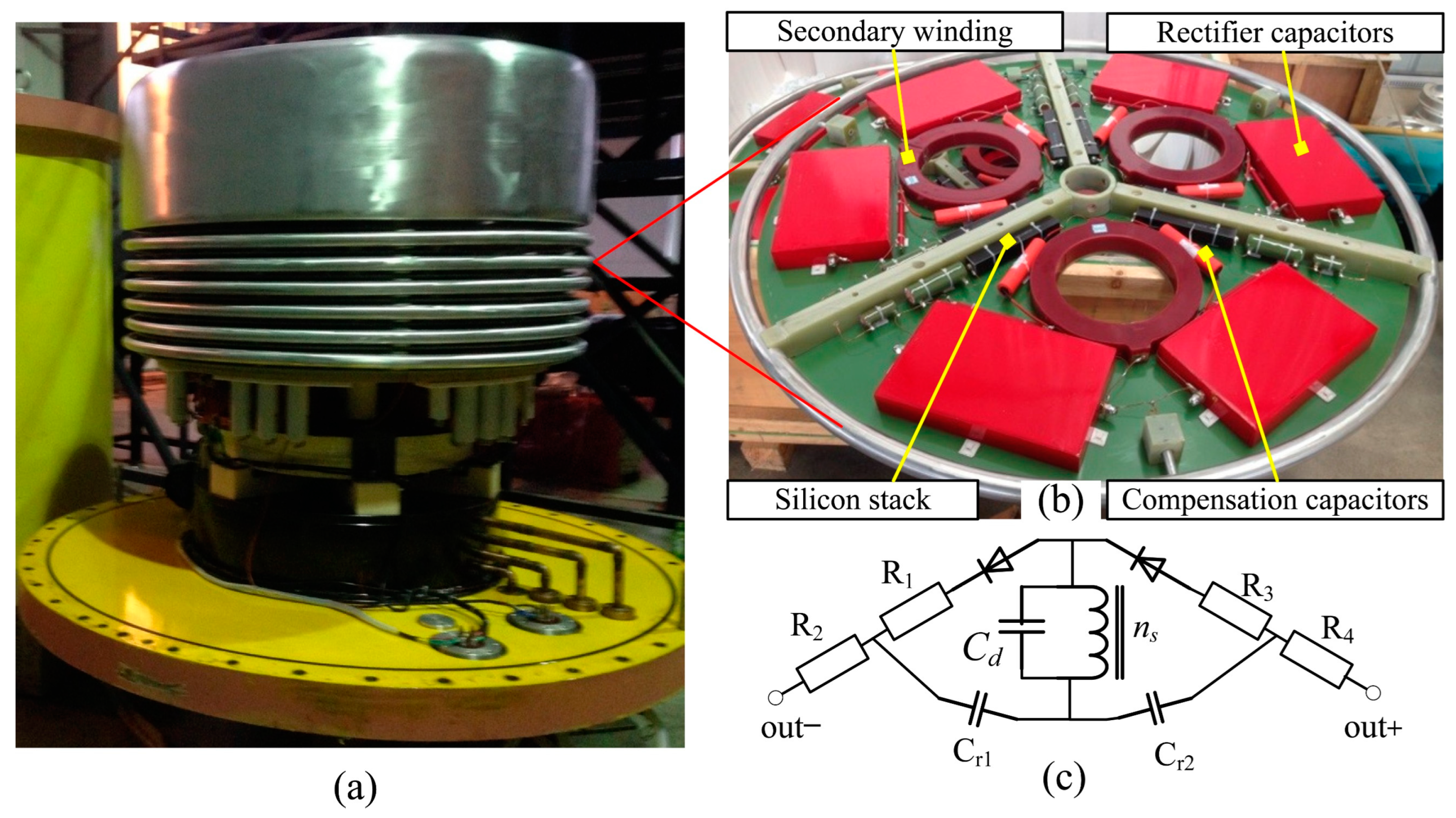
The full-parameter compensation method (FPC) [16] combines both turns compensation and capacitor compensation methods. In this approach, ns and Cs are optimized so that each stage can achieve a similar output voltage and load regulation. For instance, in a study conducted by [17], a genetic algorithm was utilized to simultaneously optimize ns and Cs, resulting in significant improvement in the performance of a six-layer three-phase ICT. Figure 2 displays a photograph of the rectifier stage in the HUST-ICT [17].

3. Unified Circuit Model and Simulation Method

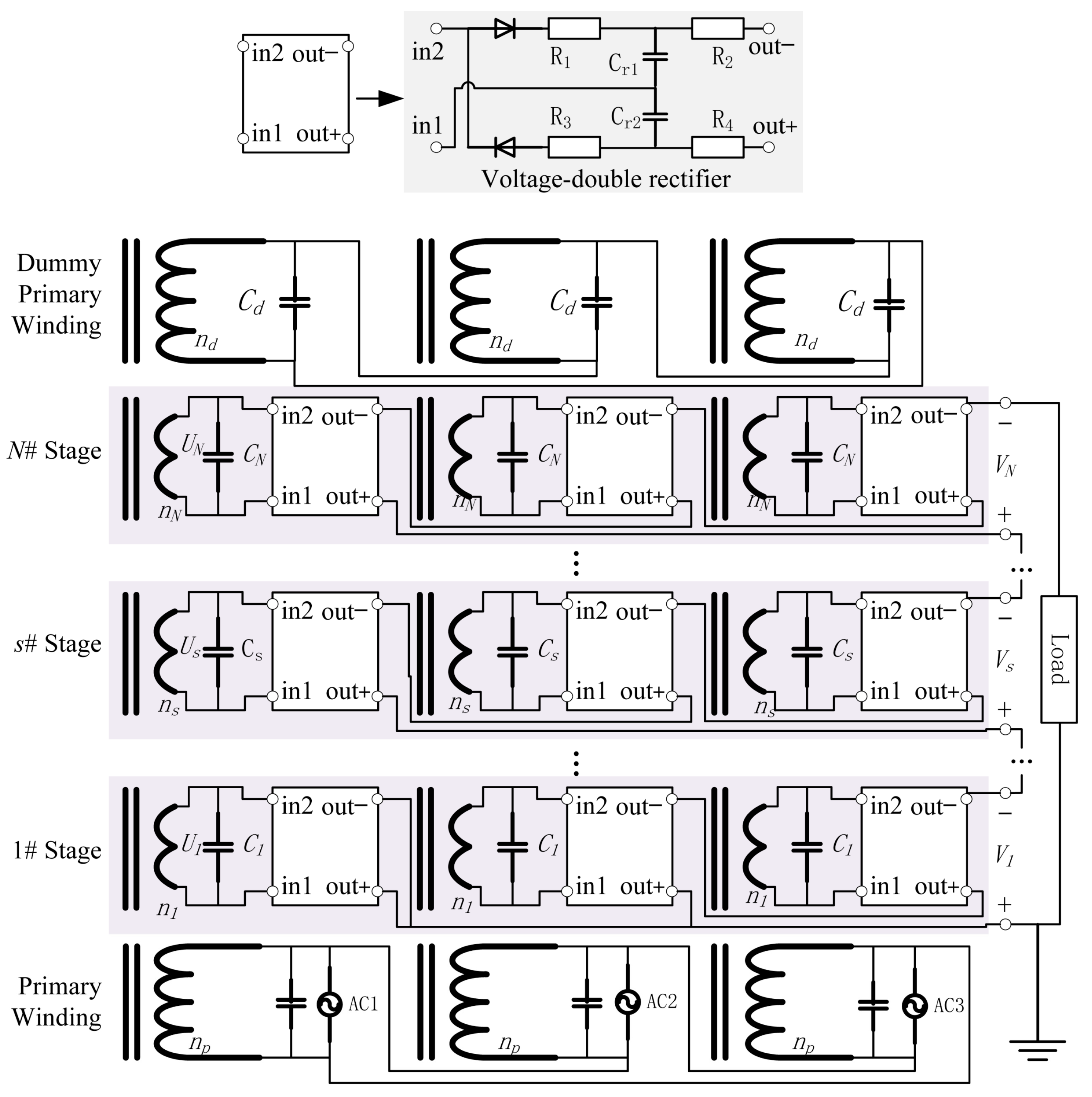
To facilitate the implementation of the optimization algorithm for the four compensation methods, a unified circuit simulation model (Figure 3) is presented. This model serves as a comprehensive circuit diagram that describes all four compensation methods, including a mutual inductance matrix, compensation capacitors, and voltage multiplier rectifier circuits [22]. As depicted in Table 1, by setting different variables and constraints, the performance of the power supply can be calculated under various compensation parameters for different compensation methods. Here, nd = 0 represents the absence of the DWP, while Cs = 0 indicates no parallel compensation capacitors. Setting these parameters to zero does not affect the model or equation-solving process.
At no load, after the power supply reaches a steady state, the input current of the rectifier tends to zero and the current waveform of the secondary wingdings becomes sinusoidal. In such cases, the output voltages and currents of the windings satisfy the transformer Equation (5).
U = j ω M I + R I j ω M I
in which U = U ˙ p , U ˙ 1 U ˙ N , U ˙ d T , I = I ˙ p , I ˙ 1 I ˙ N , I ˙ d T are the column vector of the voltages and currents of the wingdings, and R is the resistance matrix of the windings, which can be neglected because the resistance of the windings is much smaller than the impedance of the capacitors.
When the secondary windings and DWP are connected in parallel with the compensation capacitors, the voltages and currents of these windings satisfy the Ohm’s law:
U ˙ x = I ˙ x / ( j ω C x )           x   =   1 N ,   d
By combining Equations (5) and (6), we can obtain U s n and I s n . When there are no compensation capacitors, I s n = 0. Then, the stage output voltage V s n after the rectifier is calculated by the formula V s n = 2 2 U s n .
Under the full-load condition, the current waveform becomes complex due to the nonlinearity of the rectifier circuit. In such cases, the voltages and currents can be calculated by a numerical method such as MATLAB/Simulink software 2016b [23]. This simulation methodology has undergone experimental validation, demonstrating that the maximum difference between the simulation results and actual experimental data in HUST-ICT is below 0.4%, with a root-mean-square error of 0.14% [16].
The V s n and V s l are transformed into normalized values by η s = V s / V max . Vmax = max ( V 1 n , V 2 n V N n , V 1 l , V 2 l V N l ). Then, the voltage nonuniformity δn and δl are calculated by Equation (7).
δ = 1 N s = 1 N V max V s V max = 1 1 N s = 1 N η s
Load regulation SL indicates the alteration in the output voltage from no load to full load, whilst the input voltage of the primary winding remains constant. This value is related to the short-circuit impedance of the transformer. The smaller the value, the greater the output current and the stronger the load-carrying capacity. It is calculated by (8).
S L = ( s = 1 N V s n s = 1 N V s l ) / s = 1 N V s n

4. Parameters of ICT for Two Energy Levels

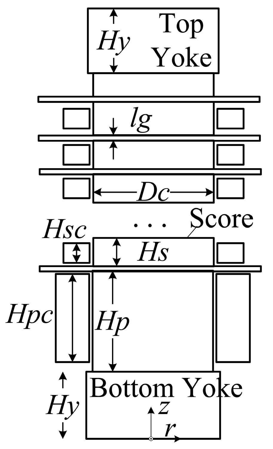
ICT high-voltage power supplies are commonly employed in accelerators with the highest beam energies below or around 1000 keV [6]. This article aims to compare the performances of four compensation methods and different optimization algorithms on ICTs with different voltage levels. Taking into account the differences in stage number N, magnetic flux leakage distribution, and application fields of ICTs with different output voltages, this article focuses on two specific examples: three-phase ICTs with output voltages of 350 kV and 1100 kV. Both are designed with a rated stage output voltage of 60 kV. The primary structural dimensions of these ICTs are presented in Table 2 and Figure 4, while the main parameters of ICT-6 remain the same as the HUST-IC [16].
Based on the structural dimensions, we established four FEM simulation models to calculate the mutual inductance matrix of single-turn wingdings M(1) for ICT-6, ICT-6 with DPW, ICT-20, and ICT-20 with DPW.
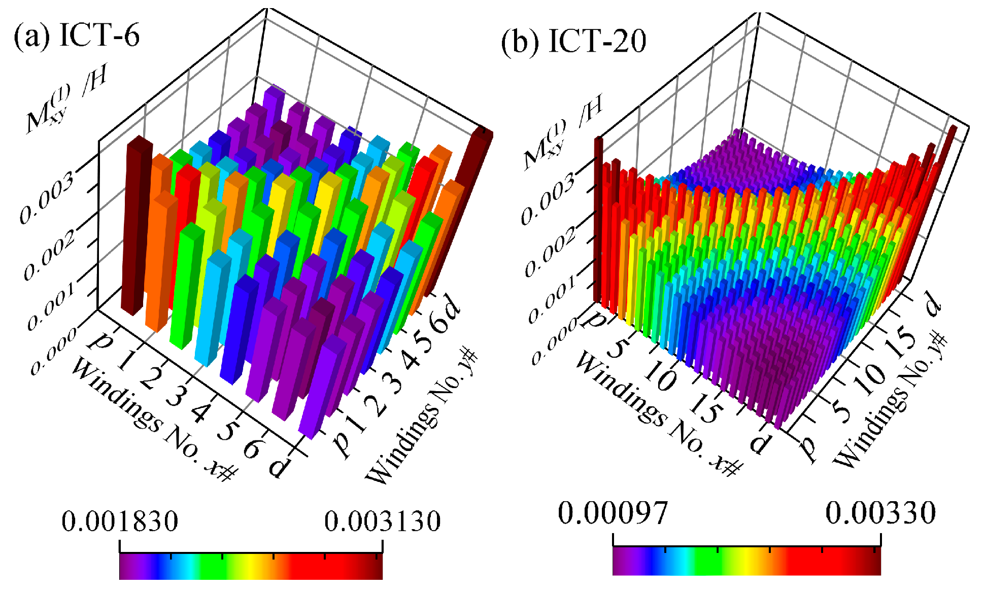
The M(1) 3D bar charts of ICT-6 with DPW and ICT-20 with DPW are shown in Figure 5a and Figure 5b, respectively, both of which exhibit saddle-shaped curves. In Figure 5b, the maximum value of M(1) is the self-inductance coefficient of the primary wingding or DWP, which is 0.0033 H. And the minimum value is M(1)dp, which is 9.6 × 10⁻⁴ H. In fact, the simulation of M(1) without DPW is basically the same as the ICT with DPW, as shown in Figure 5, exhibiting only a marginal difference of 1 × 10⁻⁵ due to slightly shorter magnetic circuits. The error between the mutual inductance matrix obtained via the FEM simulation and the actual prototype test results is less than 2.5% [16]. Therefore, the FEM result can be fully utilized to study and compare the effects of various compensation methods.

5. Optimization Algorithm

The essence of the compensation optimization is to find a set of compensation parameters (ns or Cs) that can produce the optimal value for δn, δl, and SL. This is a classic nonlinear, multi-variable, multi-objective optimization issue. For ICTs with more stages, there are more compensation parameters. Optimization algorithms such as GA and PSO can suffer from slow convergence and optimization difficulties, and it may prematurely converge to a local optimal solution [24].
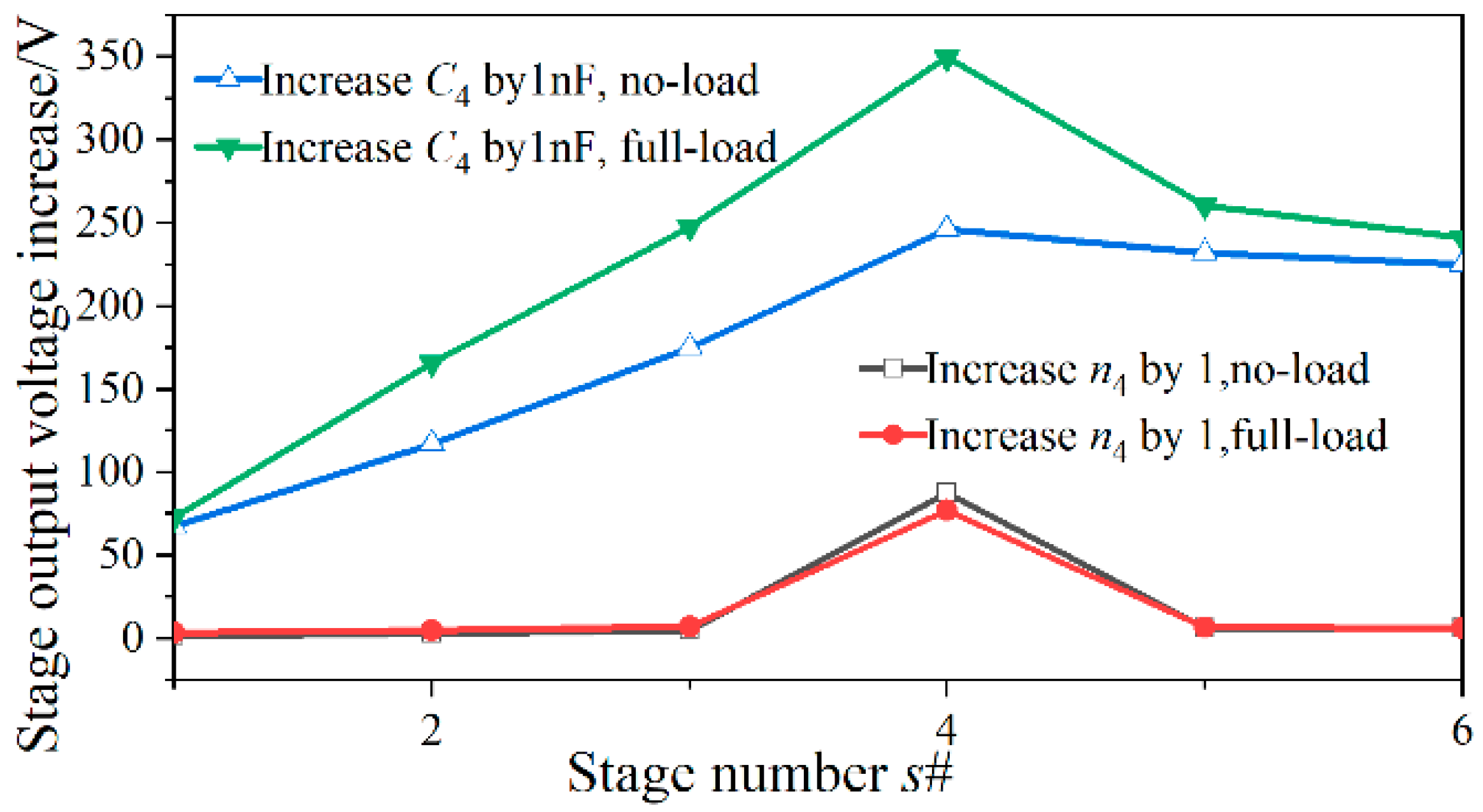
Using stage 4# of ICT-6 as a case study, the relationship between the compensation parameters and output voltage is investigated, as shown in Figure 6. It can be observed that an increase in C4 leads to an increase in all stage output voltages. This is because the excitation current generated by C4 also passes through the other secondary windings. On the other hand, an increase in n4 only affects V4, exhibiting an ideal positive correlation. Therefore, using the IM method to optimize the turns parameters will have a faster convergence, higher efficiency, and more precise optimization results. The compensation parameter changes in the other stages also have a similar compensation effect.
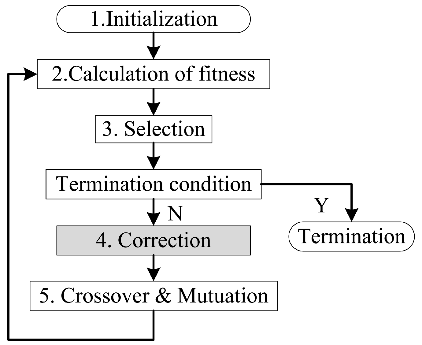
Based on these characteristics, an improved gradient-based genetic algorithm (IGGA) was proposed to optimize the compensation parameters, which combines the IM and canonical GA. It improves the search efficiency and convergence speed of the algorithm by analyzing and utilizing the gradient information to guide the evolutionary direction of the GA [25]. At the same time, after adding the gradient correction disturbance, the global convergence is improved [26]. Its calculation flow is shown in Figure 7, and its steps are briefly introduced as follows.
Step 1: A set of candidate solutions, {n1, n2, n3, … nN, C1, C2, , CN}, is created during initialization in the same way as in ref. [17].
Step 2: Calculation of fitness, which is constructed with δn, δl, SL.
f = W δ × max ( δ n , δ l ) + W S L S L
Wδ is the weight coefficient of the voltage nonuniformity and its value is set as 1. WSL is the weight coefficient of SL and its value is set as 0.1.
Step 3: Reserve the excellent candidate solutions and discard others in the selection.
Step 4: A set of fresh solutions ( C s , n s ) are generated by correcting the solution in accordance with Equations (10) and (11).
C s = C s + k c ( 1 η s m ) C max
n s = k n ( 1 η s m ) n s
Cmax denotes the maximum value of the specified solution space for the capacitor. kc and kn are the relaxation factors for the capacitance and turns, respectively. η s m = max ( η s n , η s l )
Step 5: A new generation of progeny populations is generated by crossover and mutation operations.
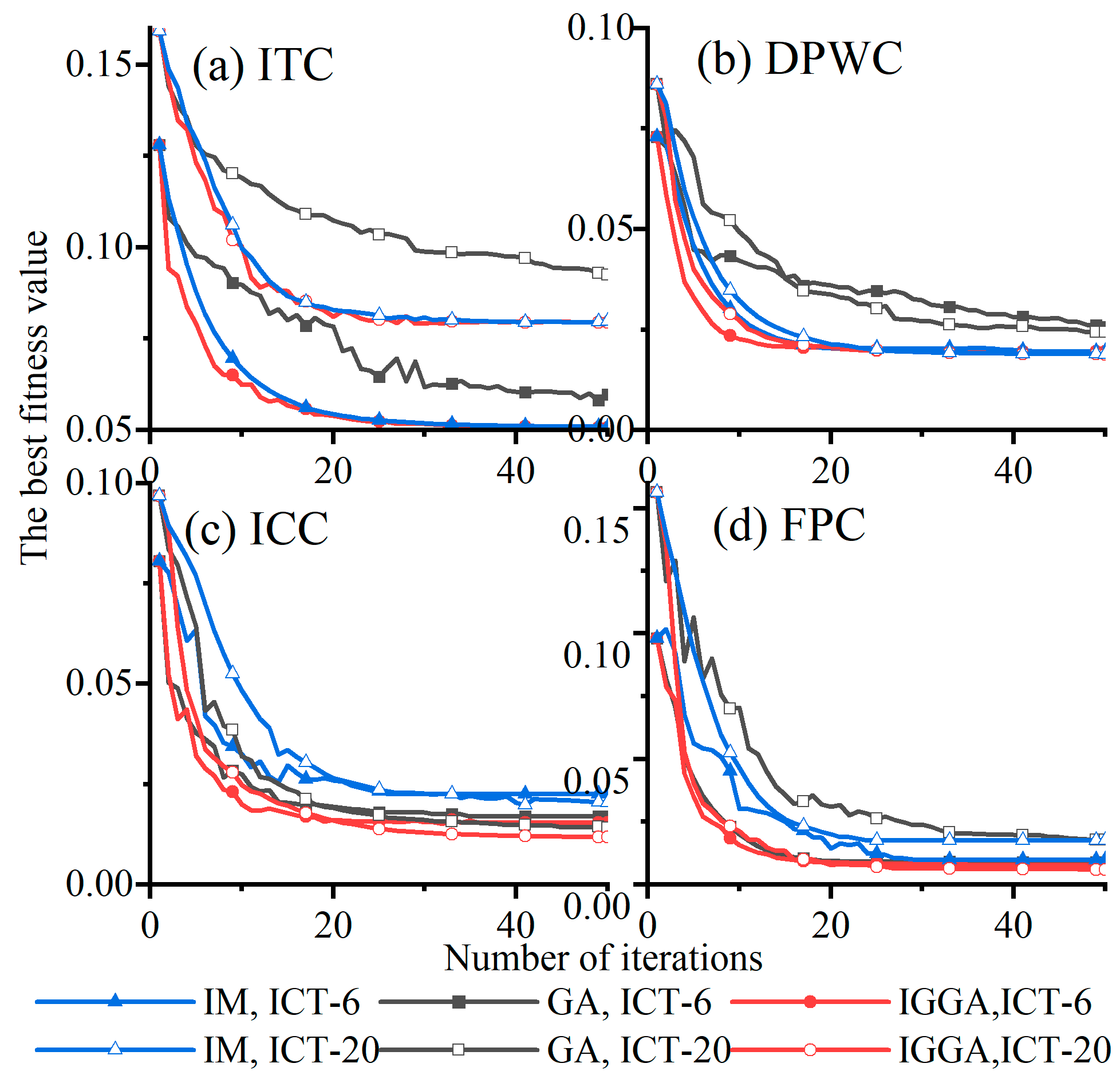
The whole process of the IGGA is implemented in the MATLAB/Simulink module with code. When the crossover rate and mutuation rate are both set to 0, the IGGA will regress to the IM. When relaxation factors kc and kn are set to 0, the IGGA will regress to the canonical GA. We utilized the IM, GA, and IGGA to optimize the four compensation methods. The convergence curves of their fitness functions are depicted in Figure 8. During the calculation, the number of populations is set to 10 times the number of stage numbers N.
Figure 8a,b show that when using the GA to optimize the ITC and DPWC, the convergence has not ended at the 50th generation, and the best fitness value is also poor. However, when the IM and IGGA are used, convergence can be achieved before 30 generations. From Figure 8c,d, it can be seen that when using the IM to optimize the ICC and FPC, the convergence speed is faster, but the best fitness value is poor and it only converges to the local optimum. Among all four compensation methods, the IGGA achieves the global optimum with the fastest convergence speed. Therefore, it is a universal algorithm for optimal ICT design. It can be seen from the comparison of the final convergence values that the minimum fitness can be obtained by optimizing the FPC method via the IGGA.

6. Comparison of Optimization Results

6.1. Optimal Compensation Parameters

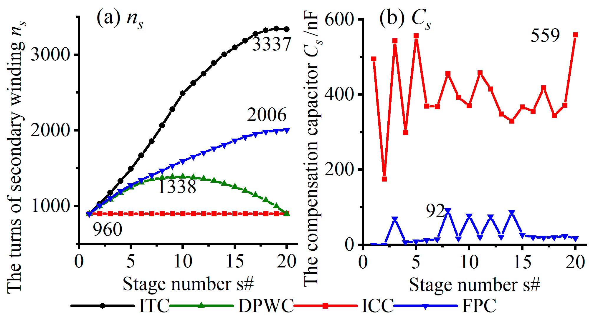
Figure 9 and Figure 10 illustrate the optimization results of the four compensation methods for two design models, ICT-6 and ICT-20, using the IGGA. It can be observed that the ITC method requires the largest number of secondary turns (ns), with ns increasing as the stage number (s) increases. For instance, in ICT-6, n1 = 2736 and n6 = 4783, while in ICT-20, n1 = 700 and n6 = 3337. In the case of the DPWC, the distributions of ns follow an inverted U-shaped pattern. In the case of the ICC, ns remains constant in each layer. However, there is no clear relationship between the Cs and s. Lastly, in the FPC method, ns also increases slightly with the s, but at a slower rate compared to the ITC method.
As shown in Figure 8 and Figure 9, the compensation parameters vary among different methods. Therefore, it is crucial to choose the suitable compensation method based on the specific requirements and characteristics of the ICT power supply design.

6.2. Optimized ICT Performance

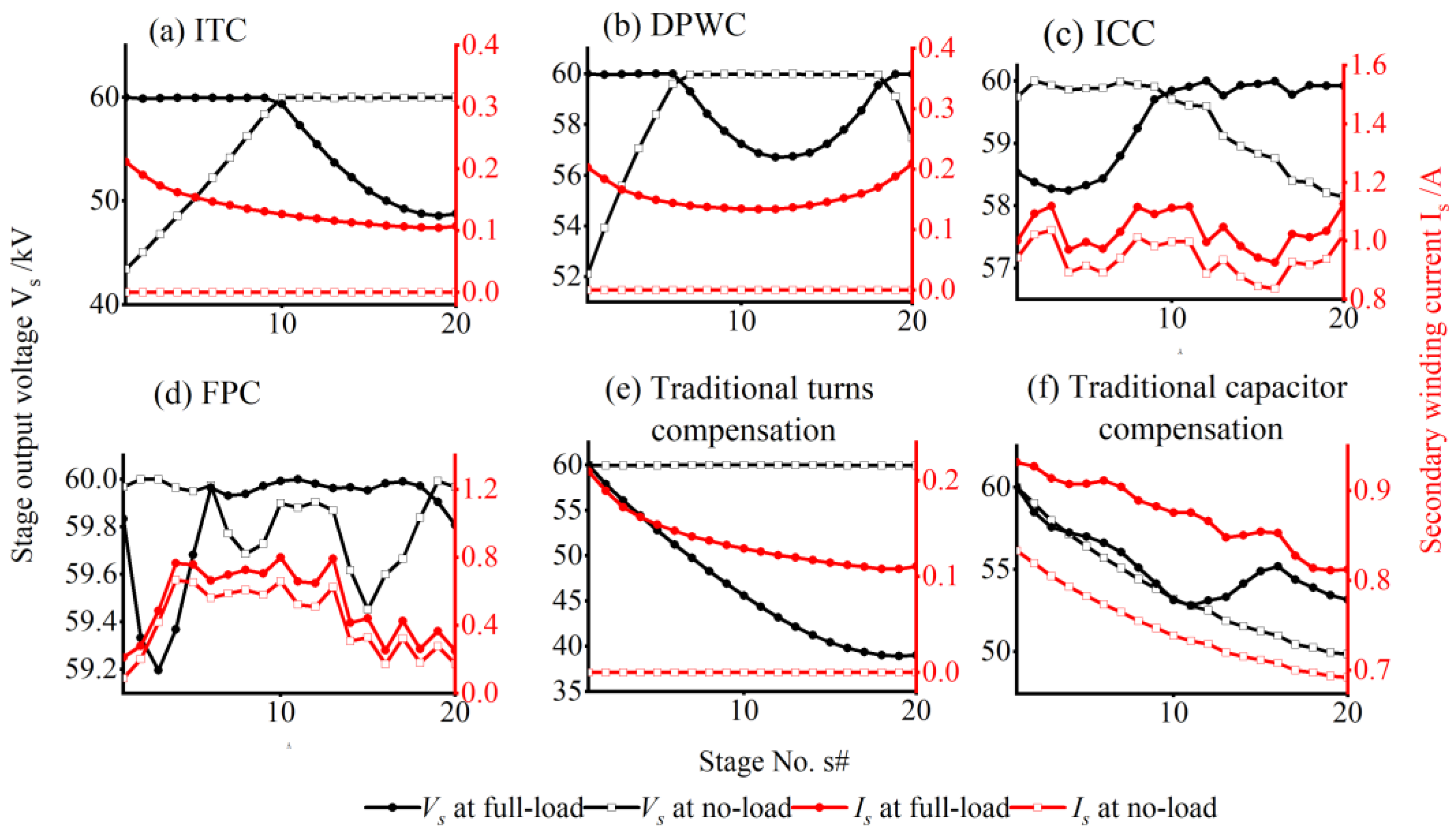
Based on the optimal compensation parameters in Figure 9 and Figure 10, the distributions of the stage output voltages vs. and the winding currents Is are calculated, as shown in Figure 11 and Figure 12. From Figure 11 and Figure 12a regarding the ITC, the vs. of ICT-6 and ICT-20 exhibit the same distribution rule. At full load, the vs. of the secondary wingdings near the primary wingdings (s < N/2) is around a rated voltage of 60 kV. However, for the other half of the secondary wingdings (sN/2), the vs. decreases with the increasing s. At no load, the distribution of vs. is exactly the opposite. From Figure 11 and Figure 12b regarding the DPWC, at full load, the vs. at both ends of the cores are around 60 kV, while the middle section sinks; conversely, at no load, the opposite pattern occurs. The Is of the full load for the ITC and DWPC are low, and the Is of the no load is 0.
Furthermore, in Figure 11 and Figure 12c,d, it can be observed that both the ICC and FPC methods exhibit a remarkably uniform stage output voltage distribution close to 60 kV. The current distributions are similar to the compensation capacitance distribution in Figure 9 and Figure 10b. Moreover, their values of Is are larger than the other two methods. Comparing between Figure 11c,d and Figure 12c,d, it can be seen that the maximum Is in ICT-20 are more than three times those in ICT-6. The reason is that ICT-20 has fewer secondary wingding turns and a larger compensation capacitance, so the currents are larger.
Comparing Figure 11e and Figure 12e with Figure 11a and Figure 12a, Figure 11f and Figure 12f with Figure 11c and Figure 12c, it can be seen that the uniformities of the improved compensation method are greatly improved compared with the traditional methods.
Finally, the statistical data of the optimized ICT performance presented in Table 3 reveal that the sorting of δn and δl for different methods is as follows: ITC > DPWC > ICC > FPC. The sorting of SL is ITC > DPWC > FPC > ICC. Additionally, with regard to the FPC method, the performance of ICT-6 and ICT-20 remains unchanged despite an increase in the number of stages.
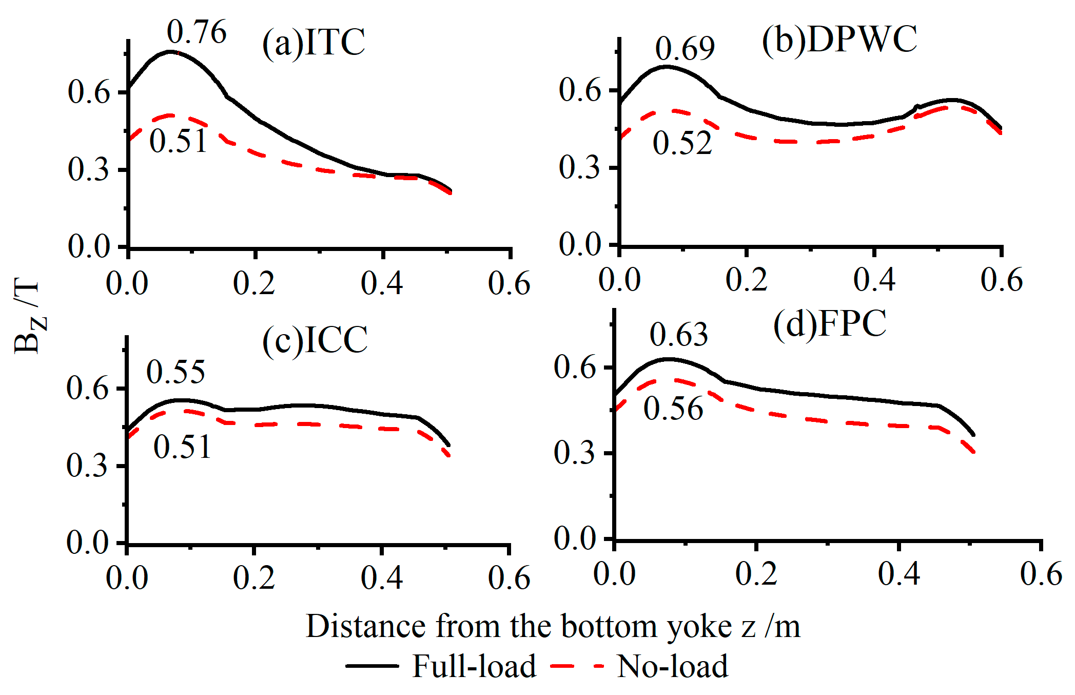
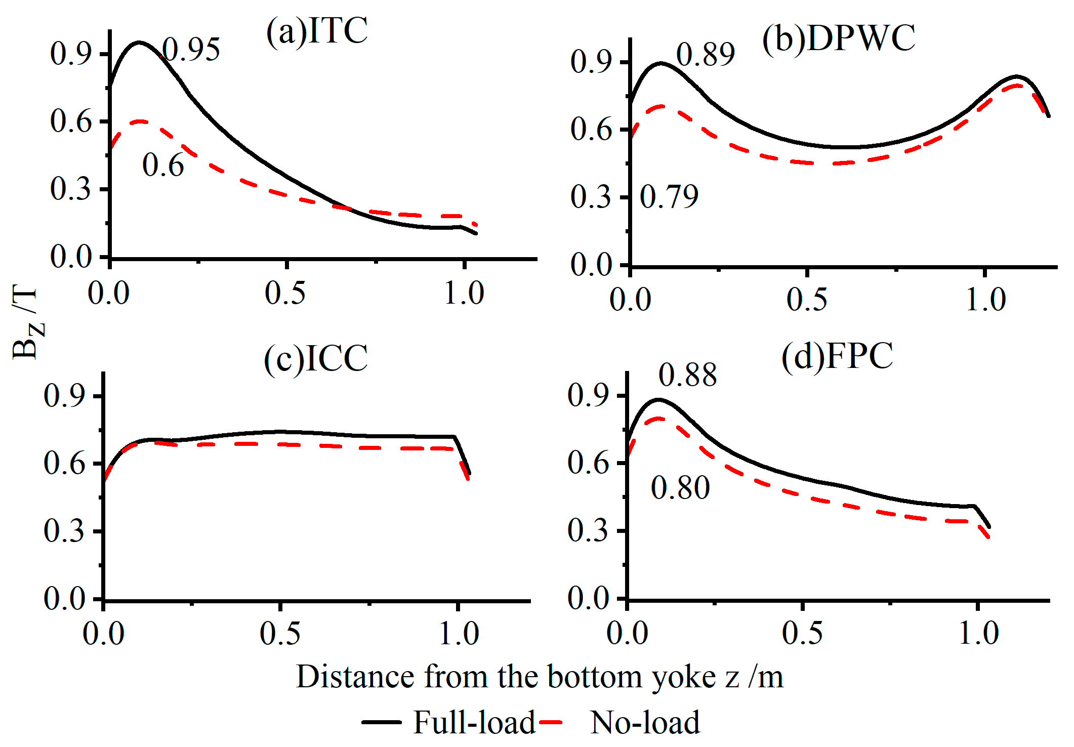
After conducting FEM simulations based on the optimal compensation parameters and winding currents Is, the magnetic field Bz curves along the z-axis on the magnetic core are obtained. By comparing Figure 13 and Figure 14, it is observed that the magnetic field curves of the two ICTs are similar, except that the magnetic field peak value of ICT-20 is slightly larger than that of ICT-6. Moreover, the ranking of the magnetic field peak values for different compensation methods is as follows: ITC > DPW > FPC > ICC. It can be inferred that the power margin of the ICT source increases as the magnetic field peak value decreases at a full load. Furthermore, the ICC has the best uniformity in magnetic field distribution, followed by the DPW. The more balanced the magnetic field distribution, the more balanced the permeability utilization will be, and the heat generation of the magnetic core is also distributed more evenly [27], thus enhancing the power supply’s carrying capacity.

6.3. Recommendations on the Selection of Compensation Methods

Based on the results of the compensation optimization, characteristics, and processing complexity discussed earlier, we can infer and analyze the suitable scenarios for different compensation methods.
(1)
The ITC does not require compensation capacitors; it only needs windings of different turns, resulting in a simple engineering implementation. However, this method exhibits poor voltage uniformity (ICT-20: 7.7%) and SL (ICT-20: 36.43%). These values indicate the high internal resistance of the power supply and limited load capacity, resulting in a low output voltage and small output current. Therefore, the method is recommended for an ICT with a lower voltage level and smaller output current.
(2)
The DPWC increases the complexity of engineering implementation more than the ITC by adding a set of DPWs and also increases the overall height of the device. Moreover, the axial magnetic field distribution is more uniform, and the peak value is smaller. Yet, it can slightly decrease δ and SL. Hence, it is recommended to use the DPWC in situations requiring a higher ICT output voltage and larger output current (greater than the ITC).
(3)
The characteristic of the ICC is that all the secondary windings have the same number of turns, and only different values of compensating capacitors need to be paralleled, making it relatively easy to implement. After undergoing this method, the winding current Is becomes larger, the magnetic field peak becomes smaller and distributed more evenly, with a low load regulation rate and robust load-carrying capacity. Therefore, it is recommended to use the ICC method in situations requiring a higher output current (greater than 200 mA). This method is applicable to ICTs of all voltage levels.
(4)
The advantage of the FPC lies in its excellent nonuniformity and relatively good load regulation suitable for ICTs with various voltage levels. Furthermore, this method is particularly suitable on some occasions where the voltage level is very high, or where the voltage distribution is required to be very uniform due to the small insulation design margin.

7. Conclusions

In this paper, a unified simulation model and an improved gradient-based genetic algorithm are proposed for four used ICT stage output voltage compensation methods (improved turns compensation, improved capacitor compensation, dummy primary winding compensation, and full-parameter compensation), which can optimize the compensation parameters quickly and efficiently. Using this model and algorithm, we optimize the parameters of the ICT at different voltage levels using the four compensation methods and comprehensively compare and analyze the effectiveness. We then summarize the compensation effect and provide suggestions for the use of the compensation methods. The unified model and optimization algorithm presented in this paper provide an effective tool for designing and analyzing a conventional ICT, and also have a certain reference value for the design of other types of ICTs such as ferrite and multi-winding transformers. Furthermore, the selection suggestions of this study fill in the blank of related research and provide a valuable reference for how to choose compensation methods in an ICT power supply design.

Author Contributions

Conceptualization, L.Y.; Software, L.Y.; Writing—original draft, L.Y.; Writing—review & editing, X.L.; Visualization, X.L.; Supervision, J.Y.; Project administration, J.Y.; Funding acquisition, J.Y. All authors have read and agreed to the published version of the manuscript.

Funding

This research received no external funding.

Data Availability Statement

Data are contained within the article.

Conflicts of Interest

Author Lei Yang was employed by the company China Electronics Technology Group Corporation. Author Xialing Liu was employed by the company NARI Group Corporation. The remaining authors declare that the research was conducted in the absence of any commercial or financial relationships that could be construed as a potential conflict of interest.

References

  1. da Costa, J.P.d.C.; Assis, M.; Teodoro, V.; Rodrigues, A.; de Foggi, C.C.; San-Miguel, M.A.; do Carmo, J.P.P.; Andres, J.; Longo, E. Electron beam irradiation for the formation of thick Ag film on Ag3PO4. RSC Adv. 2020, 10, 21745–21753. [Google Scholar] [CrossRef] [PubMed]
  2. Park, J.-H.; Ahn, J.-W.; Kim, K.-H.; Son, Y.-S. Historic and futuristic review of electron beam technology for the treatment of SO2 and NOx in flue gas. Chem. Eng. J. 2019, 355, 351–366. [Google Scholar] [CrossRef]
  3. Calvo, W.A.P.; Duarte, C.L.; Machado, L.D.B.; Manzoli, J.E.; Geraldo, A.B.C.; Kodama, Y.; Silva, L.G.A.; Pino, E.S.; Somessari, E.S.; Silveira, C.G. Electron beam accelerators—Trends in radiation processing technology for industrial and environmental applications in Latin America and the Caribbean. Radiat. Phys. Chem. 2012, 81, 1276–1281. [Google Scholar] [CrossRef]
  4. Egerton, R. Mechanisms of radiation damage in beam-sensitive specimens, for TEM accelerating voltages between 10 and 300 kV. Microsc. Res. Technol. 2012, 75, 1550–1556. [Google Scholar] [CrossRef] [PubMed]
  5. Ramachandramoorthy, R.; Bernal, R.; Espinosa, H.D. Pushing the envelope of in situ transmission electron microscopy. ACS Nano 2015, 9, 4675–4685. [Google Scholar] [CrossRef]
  6. Machi, S. Trends for electron beam accelerator applications in industry. Rev. Accel. Sci. Technol. 2011, 4, 1–10. [Google Scholar] [CrossRef]
  7. Frost, R.; Lewin, P.; Spong, M. An investigation into the suitability of insulated core transformer technology for an ultra high voltage power supply. IEEE Trans. Dielectr. Electr. Insul. 2019, 26, 501–507. [Google Scholar] [CrossRef]
  8. Frost, R.; Pilgrim, J.; Lewin, P.; Spong, M. An investigation into the next generation of high density, ultra high voltage, power supplies. In Proceedings of the 2018 IEEE International Power Modulator and High Voltage Conference (IPMHVC), Jackson, WY, USA, 3–7 June 2018; pp. 156–161. [Google Scholar]
  9. Jiang, C.; Yang, J.; Fan, M. Application of Particle Swarm Optimization in the Design of an ICT High-Voltage Power Supply with Dummy Primary Winding. Electronics 2021, 10, 1866. [Google Scholar] [CrossRef]
  10. Wang, W.; Liu, Y.; He, J.; Ma, D.; Hu, L.; Yu, S.; Li, S.; Liu, J. An improved design procedure for a 10 kHz, 10 kW medium-frequency transformer considering insulation breakdown strength and structure optimization. IEEE J. Emerg. Sel. Top. Power Electron. 2022, 10, 3525–3540. [Google Scholar] [CrossRef]
  11. Van De, G.R.J. High Voltage Electromagnetic Apparatus Having an Insulating Magnetic Core. U.S. Patent No. 3,187,208, 1 June 1965. [Google Scholar]
  12. Van De, G.R.J. High Voltage Electromagnetic Chargedparticle Accelerator Apparatus Having an Insulating Magnetic Core. U.S. Patent No. 3,323,069, 30 May 1967. [Google Scholar]
  13. Kang, C.; Liu, Y.; Li, D. Analysis of Output Voltage on a Planar Insulating Core Transformer. Nucl. Sci. Tech. 2021, 23, 15–18. [Google Scholar]
  14. Cross, J.D. Modular High Voltage Power Supply with Integral Flux Leakage Compensation. U.S. Patent No. 6,026,004, 15 February 2000. [Google Scholar]
  15. Cheng, K.; Yonghao, L.; Jianming, H.; Deming, L. Compensation of leakage flux on insulated core flat winding transformer. High Power Laser Part. Beams 2012, 24, 1595–1598. [Google Scholar] [CrossRef]
  16. Yang, L.; Yang, J.; Liu, K.; Qin, B.; Chen, D. A combined compensation method for the output voltage of an insulated core transformer power supply. Rev. Sci. Instrum. 2014, 85, 063302. [Google Scholar] [CrossRef]
  17. Yang, L.; Liu, X.; Yang, J. A new compensation method for insulated core transformer power supply and its optimization using genetic algorithm. Nucl. Instrum. Methods Phys. Res. Sect. A Accel. Spectrometers Detect. Assoc. Equip. 2020, 960, 163585. [Google Scholar] [CrossRef]
  18. Marini, F.; Walczak, B. Particle swarm optimization (PSO). A tutorial. Chemom. Intell. Lab. Syst. 2015, 149, 153–165. [Google Scholar] [CrossRef]
  19. Xu, J.; Liang, X.; Yao, X.; Liao, W. Calculation of the composite short-circuit impedance and circulating current based on the equivalent single-turn inductance matrix. In Zhongguo Dianji Gongcheng Xuebao (Proceedings of the Chinese Society of Electrical Engineering); Chinese Society for Electrical Engineering: Beijing, China, 2011; pp. 135–141. [Google Scholar]
  20. Jaraczewski, M.; Sobczyk, T. Leakage inductances of transformers at arbitrarily located windings. Energies 2020, 13, 6464. [Google Scholar] [CrossRef]
  21. Uhmeyer, U. KSI’s Cross Insulated Core Transformer Technology; AIP Conference Proceedings; American Institute of Physics: College Park, ML, USA, 2009; pp. 1099–1103. [Google Scholar]
  22. Zhang, J.; Luo, L.; Aggarwal, R.; Li, Y.; Liu, F. Simulation model’s design of a new converter transformer based on multi-coil coupling. Diangong Jishu Xuebao/Trans. China Electrotech. Soc. 2010, 25, 68–79. [Google Scholar]
  23. Luo, M.; Dujic, D.; Allmeling, J. Leakage flux modeling of medium-voltage phase-shift transformers for system-level simulations. IEEE Trans. Power Electron. 2018, 34, 2635–2654. [Google Scholar] [CrossRef]
  24. Mahdavi, M.; Javadi, M.S.; Catalão, J.P. Integrated generation-transmission expansion planning considering power system reliability and optimal maintenance activities. Int. J. Electr. Power Energy Syst. 2023, 145, 108688. [Google Scholar] [CrossRef]
  25. Sagawa, D.; Tanaka, K. Machine Learning-Based Estimation of COP and Multi-Objective Optimization of Operation Strategy for Heat Source Considering Electricity Cost and On-Site Consumption of Renewable Energy. Energies 2023, 16, 4893. [Google Scholar] [CrossRef]
  26. Mahdavi, M.; Kimiyaghalam, A.; Alhelou, H.H.; Javadi, M.S.; Ashouri, A.; Catalão, J.P. Transmission expansion planning considering power losses, expansion of substations and uncertainty in fuel price using discrete artificial bee colony algorithm. IEEE Access 2021, 9, 135983–135995. [Google Scholar] [CrossRef]
  27. Nie, L.; Yang, J.; Tang, K. Thermal Network Modeling of High Frequency Insulated Core Transformers. IEEE Trans. Appl. Supercond. 2022, 32, 0600805. [Google Scholar] [CrossRef]
Figure 1. Magnetic circuit structure of the ICT (insulated core transformer). The “d” represents the dummy primary wingding. The “p” represents the primary wingding. The “s” represents the secondary winding, and its value varies from 1 to N.
Energies 17 00547 g001
Figure 2. The photograph of HUST-ICT power supply. (a) Photograph of HUST-ICT without pressure tank. (b) Rectifier stage with full-parameter compensation method in HUST-ICT. (c) The circuit schematic diagram of one-third of rectifier disk.
Energies 17 00547 g002
Figure 3. The unified circuit simulation model of ICT.
Energies 17 00547 g003
Figure 4. Dimensions of one phase in an ICT. Its dimension parameters are in Table 2.
Energies 17 00547 g004
Figure 5. The M(1) 2D bar charts of ICT-6 with DPW (a) and ICT-20 with DPW (b).
Energies 17 00547 g005
Figure 6. Increase in stage voltage output caused by increasing the compensation capacitor C4 by 1nF and the number of secondary wingdings turns n4 by 1.
Energies 17 00547 g006
Figure 7. The calculation flow of improved gradient-based genetic algorithm.
Energies 17 00547 g007
Figure 8. Convergence curves of the optimization process for the four compensation methods. The vertical axis is the fitness value of the best individual among all candidate solutions in each generation.
Energies 17 00547 g008
Figure 9. The optimal compensation parameters of ICT-6 optimized by four compensation methods: (a) turns ns and (b) capacitance Cs.
Energies 17 00547 g009
Figure 10. The optimal compensation parameters of ICT-20 optimized by four compensation methods: (a) turns ns and (b) capacitance Cs.
Energies 17 00547 g010
Figure 11. Stage output voltages vs. and winding currents Is of ICT-6 with different compensation methods.
Energies 17 00547 g011
Figure 12. Stage output voltages vs. and winding currents Is of ICT-20 with different compensation methods.
Energies 17 00547 g012
Figure 13. The distribution curve of the axial magnetic field Bz of the core along the z-axis in ICT-6.
Energies 17 00547 g013
Figure 14. The distribution curve of the axial magnetic field Bz of the core along the z-axis in ICT-20.
Energies 17 00547 g014
Table 1. The variables and constraints of different compensation methods.
ConstraintsVariables
ITCnd = 0, Cd = 0, Cs = 0ns
DPWCnd = np, Cd is from Equation (2), Cs = 0ns
ICCnd = 0, Cd = 0, ns is from Equation (1)Cs
FPCnd = 0, Cd = 0Cs, ns
Table 2. The dimensional parameters of two typical ICT structures.
ICT-6ICT-20
N620
Dc/mm178250
Score/mm22.3 × 1044.9 × 104
np, nd9232
lg/mm22
Hs/mm45.638
Hp/mm125170
Hsc/mm31.527.5
Hpc/mm155190
Yoke diameter/mm660960
Hy/mm100120
Table 3. Comparison of (δl and δn) and load regulation rate (SL) with different compensation methods.
ITCDPWICCFPC
ICT-6δn4.32%1.64%1.53%0.52%
δl4.32%1.65%1.53%0.52%
SL32.81%24.4%7.48%11.38%
ICT-20δn7.74%2.20%1.30%0.51%
δl7.71%2.18%1.07%0.43%
SL36.43%21.1%2.70%12.16%
Disclaimer/Publisher’s Note: The statements, opinions and data contained in all publications are solely those of the individual author(s) and contributor(s) and not of MDPI and/or the editor(s). MDPI and/or the editor(s) disclaim responsibility for any injury to people or property resulting from any ideas, methods, instructions or products referred to in the content.