Abstract
Due to the insulation saturation effect of a vacuum gap, the series connection is the main method to improve the capability of the triggered vacuum switch (STVS) to withstand voltage. In this paper, a double-gap surface flashover triggered multistage vacuum switch (DMVS) is constructed based on a removable vacuum chamber. The DMVS consists of a surface flashover triggered vacuum gap (STG) and a self-breakdown vacuum gap (SBG) in series. The trend in DMVS conduction delay time under different operating parameters and gap distances is firstly measured through experiments, and then the conduction delay time characteristics of DMVS and single-gap STVS compared. The test results show that increasing the trigger current and operating voltage and decreasing the gap distance of each vacuum gap can optimize the conduction delay time of the DMVS, but the voltage division ratio between the STG and the SBG has no obvious influence on the conduction delay time. The comparison result between the DMVS and the STVS shows that increasing the number of series gaps increases the conduction delay time but, for a certain vacuum gap distance, DMVS exhibits superior conduction delay time characteristics compared to STVS.
1. Introduction
The triggered vacuum switch (TVS) is a kind of fast closing switch combining vacuum switch technology and three electrode spark technology, which has the advantages of strong insulation recovery ability, short trigger time, small arc erosion ability and low noise [1,2,3,4,5,6]. The TVS can be mainly categorized into the laser triggered vacuum switch (LTVS) and the electrically triggered vacuum switch (ETVS). The LTVS requires expensive laser trigger systems, which limit its large-scale application to a certain extent [7,8]. The ETVS is widely used in electrical system protection, electromagnetic emissions, high power lasers, particle beam devices and other pulsed power systems due to its simple structure, low cost and low requirements for the working environment [9,10]. The ETVS can be divided into the field breakdown triggered vacuum switch (FTVS) and the surface flashover triggered vacuum switch (STVS), among which the STVS has the advantages of high stability for conduction delay and low trigger threshold. The operating principle of the STVS is that the trigger gap firstly experiences surface flashover breakdown under the action of an external high voltage pulse used to generate the initial plasma. Subsequently, the initial plasma diffuses into the main gap, causing its breakdown [11].
The TVS is an important component of the pulsed power system, and its operating performance determines its output waveform [12]. In recent years, a large number of scholars have conducted in-depth research on the operating performance of the STVS. Yao et al. investigated the effect of the dielectric constant of the surface flashover material on the conduction delay time and designed a z-structure trigger electrode to optimize the operating life of the STVS [13]. Hu et al. studied the generation characteristics of the initial plasma from the trigger gap [14]. Zhou et al. proposed a heat conduction model for approximate computation of conduction delay time [15]. Wu et al. researched the through-current capability of a six-gap multi-rod electrode TVS, with a maximum through-current capability of 200 kA [16]. Park et al. designed an STVS with a ring trigger electrode based on BaCO3 dielectric material and measured its conduction delay time [17]. Wang et al. investigated the operating life and delay time characteristic of a six-gap multi-rod electrode STVS, and the test results show that the operating life of this STVS is greater by 1000 times, and the conduction delay time is around 2.5 μs [18].
Obviously, previous work has focused on the study of the operating performance of the single-gap STVS. However, the static voltage withstand characteristic is the main technical index to be considered for a vacuum switch. Due to the insulation saturation effect of the vacuum gap, the static voltage withstand characteristic cannot be improved simply by increasing the gap distance of the single-gap STVS [19,20]. Therefore, in this paper, based on the voltage withstand gain of series connected vacuum gaps, a surface flashover triggered multistage vacuum switch (SMVS) structure is designed, which consists of a surface flashover triggered vacuum gap (STG) and multiple self-breakdown vacuum gaps (SBG) connected in series. High static voltage withstand capability of the SMVS can be achieved by adjusting the number and distance of series vacuum gaps. In addition, this paper builds a double-gap SMVS (DMVS) prototype using a removable vacuum chamber based on the operating characteristic of the proposed SMVS. The closing performance of the DMVS under different operating parameters and gap distances is measured, the mechanism of the influence of different parameters on the conduction delay time characteristic of the DMVS is analyzed, the delay time characteristic of the DMVS is compared with that of the single-gap STVS, and a reasonable design suggestion for the SMVS is given.
2. SMVS Structure and Experimental Platform
2.1. Series Gain Characteristics of Vacuum Gaps
For a vacuum switch, generally, when the electrode gap distance is greater than 6 mm, this demonstrates a more obvious voltage saturation effect. The relationship between the corresponding breakdown voltage and vacuum gap distance can be expressed as in Equation (1) [21]:
where Ub is the breakdown voltage of the vacuum gap, d is the gap distance of the vacuum gap, k is a constant term, and α is a constant term with a value range of 0.4–0.7.
By connecting n vacuum gaps with the same gap distance in series and approximating the partial voltage between each vacuum gap as uniform and homogeneous, the total breakdown voltage can be expressed as Equation (2):
where Unb is the total breakdown voltage of n vacuum gaps connected in series.
If the gap distance of the vacuum gap is directly increased by a factor of n, the corresponding breakdown voltage is Equation (3):
where Ubn is the breakdown voltage for a vacuum gap distance of nd.
Comparison of Unb and Ubn gives the gain factor Gn for breakdown voltage after splitting a vacuum gap with a gap distance of nd into n vacuum gaps with a gap distance of d.
It is clear from Equation (4) that the voltage withstand capacity when connecting n short vacuum gaps in series is greater than when directly increasing the vacuum gap distance by n times. Although, in practical applications, the uneven partial voltage of the individual gaps results in a lower actual gain factor, the series connection of several vacuum gaps remains the main means of optimizing the voltage withstand characteristic of the vacuum gap.
2.2. SMVS Structure
The basic structure of the designed SMVS is shown in Figure 1. Due to the co-electrode structure of the trigger electrode cathode and the main electrode cathode of the SVG, the STG can only be placed on the low voltage side of the SMVS. Multiple SBGs are axially stacked and connected to form a cascade gap, with the support insulator located in the middle of the electrodes. The anode of the STG is connected equipotentiality to the cathode of the cascade gap, and the anode of the cascade gap is connected to the external circuit as the anode of the entire switch. The electrode gap distance is the same for each SBG. A shield is placed on the outside of each vacuum gap inside the SMVS to absorb the metal vapors generated by the vacuum arc ablating the metal electrodes during the conduction phase and to ensure the insulation of the inner wall of the insulation shell. The internal structure of the STG is consistent with the structure of a typical STVS.
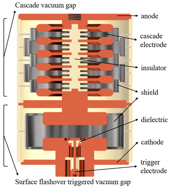
Figure 1.
Schematic diagram of the basic structure of the SMVS.
2.3. Experimental Platform
When the cascade gap is equated to an SBG with a large self-breakdown voltage, the SMVS can be simplified to a DMVS structure for analysis, so a DMVS test prototype is built in this paper for experimental study. As shown in Figure 2, the DMVS test platform is built, based on a removable vacuum chamber, where the lower gap of the vacuum chamber is an STG and the upper gap is an SBG. The gas pressure inside the chamber is controlled below 10−4 pa by mechanical and molecular pumps. The trigger electrode of the STG is connected to the external trigger circuit through an extended electrode below the chamber. The electrode material is stainless steel and the trigger electrode material is copper. The gap distance between the SBG is adjusted by the thickness of the intermediate insulation gasket.
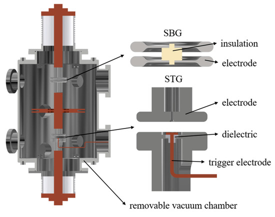
Figure 2.
The Schematic Diagram of the DMVS test prototype and electrode structure.
The experimental circuit mainly includes the trigger circuit and the main gap discharge circuit, and its equivalent circuit is shown in Figure 3, where PTM0, PTM1 and PTM2 are high voltage probes, the measured value of PTM1 is the voltage of the STG, and the voltage at the two ends of the SBG is the difference between the measured values of the two voltage probes PTM0 and PTM1. CM0 and CM1 are the discharge capacitors for the main and trigger circuits, both of which are 8.9 μF. RM0 and RM1 are load water resistors for the main and discharge circuits. Stray inductance is LM0, and LM1 for the main circuit and the trigger circuit. RPar1 and Rpar2 are high voltage non-inductive resistors used to regulate the relationship between the two gap partial voltages, where RPar1 is fixed at 6 MΩ. The LTVS in the trigger circuit is used as a closing switch for the circuit to control the moment of applying the external high voltage pulse. The LTVS can stabilize the rising edge of the trigger high voltage pulse on the order of ns. During the experiment, the energy storage capacitors CM1 and CM2 are first charged, and then the DMVS is triggered by the laser controlling the LTVS closing to break down the trigger gap of the STG. After the DMVS is triggered, the main circuit begins to discharge.
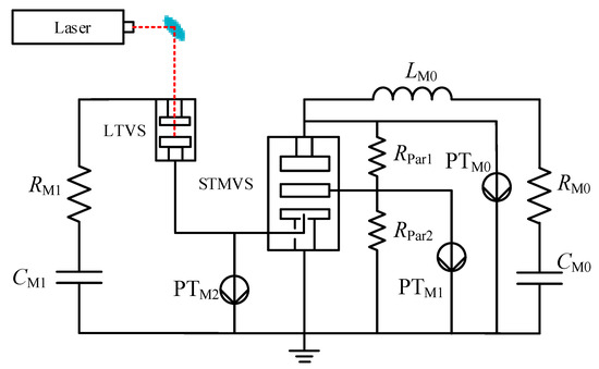
Figure 3.
Equivalent circuit of the experimental platform.
3. Analysis of DMVS Closing Process
3.1. Principle of STVS Operation
The STVS can carry a high voltage across its main gap when it is not triggered. When the trigger gap undergoes surface flashover breakdown with an external high voltage trigger signal, initial plasma is generated at the cathode of the STVS. After the STVS is triggered, it enters the vacuum gap spark discharge phase. In this phase, the cathode plasma expands toward the anode and, when the cathode plasma expands to the anode, the STVS completely closes and the discharge turns to the vacuum arc phase. When the vacuum gap discharge enters the arc phase, the voltage at both ends of the STVS reaches a stable minimum. Obviously, the speed of the STVS closing process depends on the distance of the vacuum gap and the expansion velocity of the cathode plasma.
For the analysis of the cathode plasma velocity, Plyutto proposed an ambipolar acceleration model for a spherically expanded plasma to describe the diffusion of the cathode plasma during the vacuum spark stage. The model suggests that, since the electron velocity is much greater than the ion velocity, the electron concentration gradient is responsible for the acceleration of ions. The ambipolar accelerating field strength and the corresponding potential difference are shown in Equations (5) and (6) [22,23].
where kb is the Boltzmann constant, Te is the electron temperature, nem is the maximum electron concentration and nex is the concentration of the electron at a point in space. φem is the corresponding potential at nem, and φex is the corresponding potential at nex.
3.2. DMVS Closing Process
Figure 4 shows the typical waveforms of the conduction stage of the DMVS, and Figure 5 shows the corresponding voltage test positions of the DMVS prototype. UDMVS is the operating voltage at both ends of the DMVS, USTG is the STG voltage, USBG is the SBG voltage, and Utri is the voltage of the trigger gap. ts is the SBG breakdown delay, which is the time for the operating voltage to be fully transferred to the STG gap, and tc is the DMVS conduction delay time. According to the definition of STVS delay time, it can be seen that the DMVS conduction delay time tc is defined as the time range from the start of the trigger gap voltage drop to the time when the operating voltage drops to its lowest point [18,19].
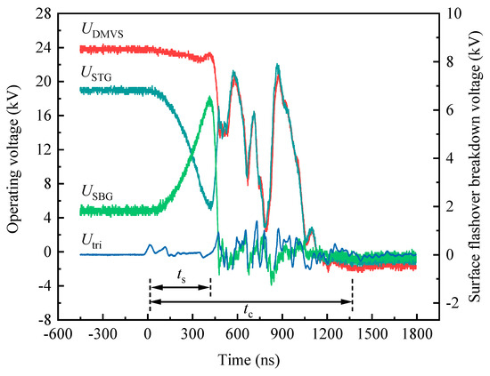
Figure 4.
The typical voltage waveform of the DMVS.
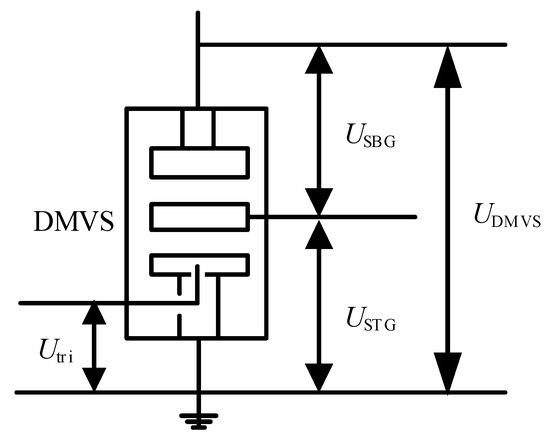
Figure 5.
Schematic diagram of each gap voltage in the DMVS.
Based on the voltage waveform of the DMVS, the closing process can be divided into three phases. Firstly, after the trigger gap is broken down by an external high-voltage pulse, initial plasma is formed on the cathode surface of the STG, which creates an electron current toward the STG anode (SBG cathode), i.e., the STG transfers charge to the SBG. Therefore, the voltage USTG at the ends of the STG drops rapidly at this phase and is superimposed on the SBG as a shock voltage, causing the voltage USBG at the ends of the SBG to rise rapidly. After a certain delay time, the rise of the voltage USBG at both ends of the SBG leads to field breakdown of the SBG. Meanwhile, the DMVS is triggered, causing the total operating voltage UDMVS to begin to fall. The second phase is the rapid closing of the SBG to transfer the operating voltage to the STG. The closing process of the SBG is much faster than that of the STG due to the shorter gap distance of the SBG and the fact that the electric field in the vacuum gap is much larger than the electric field in the STG gap when self-breakdown occurs. In this phase, with the complete closing of the SBG, the voltage USBG at its ends drops to zero at a very fast rate, resulting in the total operating voltage being fully applied to the STG. The final phase is when the cathode plasma in the STG gap expands to the anode causing the STG to completely close, the operating voltage UDMVS at both ends of the DMVS drops to a stable minimum along with the USTG, and the switch arrives as full conduction.
4. Experimental Results and Analysis
In this paper, 10 measurements are made for each set of parametric conditions, the average value is used as the conduction delay time for that parameter, and the mean square deviation is used as the jitter time for that parameter.
4.1. Influence of Trigger Current
Figure 6 shows the trigger delay characteristics of the DMVS with different trigger currents. The experimental conditions are that the operating voltage of the DMVS is 15 kV and the voltage division ratio between the two gaps of the SBG and STG is set to 1:3. The gap distance is 0.8 mm for the SBG and 4 mm for the STG. The trigger current is changed by adjusting the charging voltage of the trigger circuit storage capacitor. The trigger current varies from 2 to 10 A, increasing by 2 A each time. As can be seen from the figure, the conduction delay time has a significant decreasing trend with the increase in the trigger current. The conduction delay time corresponding to trigger currents 2 A, 4 A, 6 A, 8 A, and 10 A are 1357.8 ns, 1251.7 ns, 1111.13 ns, 1041.6 ns, and 998.1 ns, respectively. The conduction delay time under different trigger currents is analyzed by the analysis of variance (ANOVA) to obtain the corresponding F-value of 24.836, and the p-value of 6.728 × 10⁻¹¹ < 0.05, which indicates that there is a significant difference in the conduction delay time under different trigger currents tested, and the difference is statistically significant.
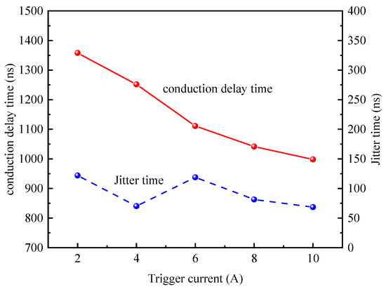
Figure 6.
The conduction delay time with different trigger currents.
From the previous analysis of the DMVS closing process, it can be seen that the conduction delay time of the DMVS ultimately depends mainly on the closing time of the STG. Increasing the trigger current on the one hand increases the initial temperature of the cathode plasma, which means increasing its initial velocity. On the other hand, higher trigger currents ablate the electrode surface more severely, which can produce a higher density of cathode plasma and increase the ambipolar accelerating field strength. Therefore, increasing the trigger current accelerates the expansion of the cathode plasma and reduces the conduction delay time of the DMVS.
4.2. Influence of Operating Voltage and Voltage Division Ratio
Set the trigger voltage to 4 A, the STG gap distance to 4 mm, and the SBG gap distance to 0.8 mm. The total operating voltage at both ends of the switch is increased from 15 kV to 2 7 kV by 3 kV each time. The voltage division ratio between the SBG and the STG is set to 1:2, 1:3, 1:4 and 1:8, respectively. The effect of operating voltage on conduction delay time for different voltage division ratios is shown in Figure 7. As can be seen from the figure, the conduction delay time of the DMVS decreases significantly with the increase in the operating voltage, but the different voltage division ratios have no obvious effect on the conduction delay time. The SBG undergoes direct self-breakdown at an operating voltage of 27 kV when the voltage division ratio is 1:2. At a voltage division ratio of 1:2 between the two gaps, with the increase in operating voltage, the test results for conduction delay time are 1157.18 ns, 1127 ns, 1098.8 ns, and 1056 ns, respectively. The conduction delay times measured at a voltage division ratio of 1:4 are 1143 ns, 1086 ns, 1087 ns, 1048.6 ns and 1014 ns, respectively. The corresponding conduction delay times for a voltage division ratio of 1:8 are 1168 ns, 1122.8 ns, 1116.5 ns, 1076 ns, and 1054 ns, respectively.
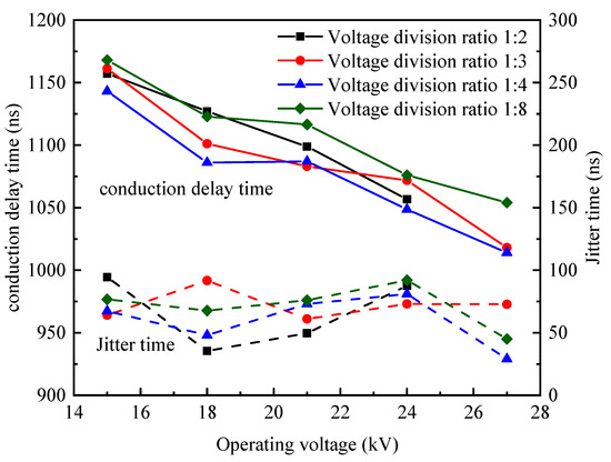
Figure 7.
Conduction delay time with different operating voltages and voltage division ratios.
In order to prove the statistical significance of the test results for conduction delay time at different operating voltages, the test results at 1:3 division ratio are selected for ANOVA, the F-value is obtained as 4.987, and the p-value is 0.002, less than 0.05. This result shows that there is a significant difference in the conduction delay time at different operating voltages, and increasing the operating voltage can reduce the conduction delay time of the DMVS.
At a constant voltage division ratio, increasing the operating voltage increases the static voltage of the SBG, and therefore reduces the breakdown time required by the SBG, and it can apply the operating voltage at both ends of the DMVS to both ends of the STG more quickly. At the same time, the increase in voltage at both ends of the STG can increase the equivalent field strength of the STG. The higher the electric field strength, and the higher the energy that the electron in the cathode plasma can obtain from the external electric field, the more energy is transferred to the ion, thus accelerating the expansion of the plasma to the anode. Therefore, the increase in operating voltage optimizes the conduction delay time of the DMVS. Although the change in the voltage division ratio changes the breakdown time of the SBG, the conduction delay time of the DMVS mainly depends on the closing time of the STG gap. With a constant operating voltage, the voltage division ratio has not changed the voltage across the STG during the final closing phase of the STG. Therefore the voltage division ratio has a small effect on the conduction delay time.
4.3. Influence of Gap Distance
In order to investigate the influence of different gap distances on the delay time characteristic of the DMVS, three sets of DMVS with different combinations of gap distances are set up for measurement in this section. The three combinations of different gap distances are 0.6 mm SBG with 4 mm STG, 1.2 mm SBG with 4 mm STG, and 1.2 mm SBG with 8 mm STG. Due to the high self-breakdown voltage required for the 1.2 mm SBG, the operating voltage is set to 24 kV, and the voltage division ratio between the SBG and STG is set to 1:4. Figure 8 shows the conduction delay time characteristic of the DMVS for three different gap distances. Both increasing the gap distance of the SBG and the STG result in a longer DMVS conduction delay time. For example, at a trigger current of 4 A, the conduction delay time is 1150.6 ns for 0.6 mm SBG and 4 mm STG, 1264 ns for 0.8 mm SBG and 4 mm STG, and 1632.2 ns for 1.2 mm SBG and 8 mm STG.
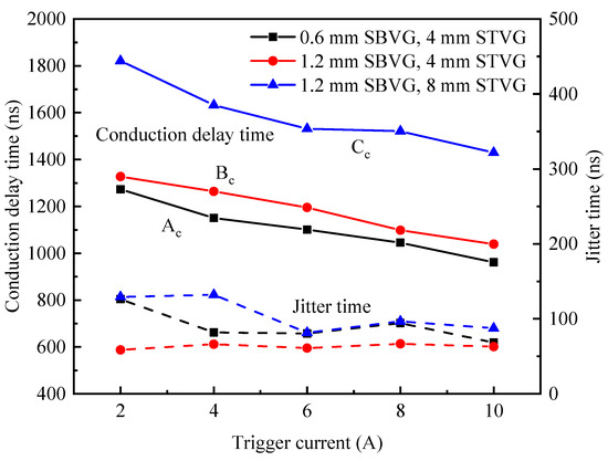
Figure 8.
Conduction delay time with different gap distances.
The conduction delay time data of 0.6 mm and 1.2 mm SBG at 6 A and 10 A trigger currents, respectively, are selected for t-test. The corresponding calculated results are t-values of 2.946 and 2.632, greater than the critical t-value of 2.101, and p-values of 8.65 × 10⁻³ and 1.69 × 10⁻² are less than 0.05, which proves that the test results are statistically significant, and SBG gap distance has an effect on the conduction delay time of the DMVS. Similarly, the conduction delay data for 4 mm and 8 mm STG gaps at 6 A and 10 A trigger currents, respectively, are selected for T-test. The corresponding t-values of 10.43 and 11.46 are greater than the corresponding critical t-value of 2.101, and the p-values of 4.672 × 10⁻⁹ and 1.05 × 10⁻⁹ are less than 0.05, which proves that the test results are statistically significant, and the change in STG gap distance has a significant effect on the DMVS conduction delay time.
The conduction delay of the DMVS mainly depends on the development of the STG cathode plasma. The increase in the SBG gap distance increases its breakdown time, resulting in a longer time required for the SBG to apply the voltage at the ends of the DMVS to the ends of the STG gap, which will affect the expansion velocity of the cathode plasma of the STG to a certain extent, and thus the increase in the SBG distance raises the conduction delay time. Lengthening the STG gap distance obviously increases the cathode plasma expansion time and prolongs the time required for the STG to close completely.
4.4. DMVS and Single-Gap STVS Conduction Delay Time Comparison
According to the saturation characteristic of the vacuum gap, it can be seen that, under the same gap length, the series connection of multiple vacuum gaps helps to increase the gap voltage withstand. According to the previous analysis, the conduction delay time of the DMVS mainly depends on the influence of STG closing speed, and SBG closing speed is much faster than that of STG, so the conduction delay time characteristic of the proposed DMVS structure should be better than the single-gap STVS for a certain total gap length of the vacuum switch. Two groups of DMVS with different gap distances are set up to compare with single-gap STVS, where the first group is 4 mm STG and 1 mm SBG, the second group is 5 mm STG and 1 mm SBG, and the gap distance of single-gap STVS is 5 mm.
The conduction delay time characteristic of DMVS and single-gap STVS is given in Figure 9. The figure shows that the trigger current is enhanced from 4 A to 16 A, and the conduction delay time of the first DMVS is reduced from 1176.6 ns to 849.8 ns; the conduction delay time of the single-gap STVS is reduced from 1264 ns to 937.3 ns; and the conduction delay time of the second DMVS is reduced from 1417.6 ns to 1005 ns. Obviously, by comparison, it can be found that, when the vacuum gap distance is certain, the conduction delay time of the DMVS is better than that of the single-gap STVS. Connecting the SBG in series when the STG gap distance is the same as the single-gap STVS gap distance will result in a poor conduction delay time.
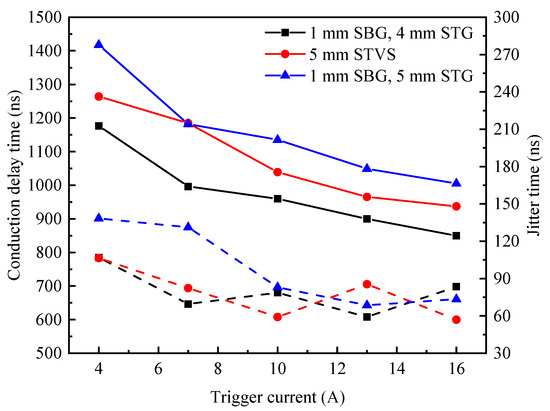
Figure 9.
Conduction delay time with different structures.
The conduction delay time test data for 10 A and 16 A trigger currents for the above three structures are analyzed by ANOVA, respectively. The corresponding F-values for 10 A and 16 A are 14.364 and 11.949, and the p-values are 4.62 × 10⁻⁵ and 1.64 × 10⁻⁴, respectively. The p-values in the calculated results are all less than 0.05, indicating that there is a significant difference in the conduction delay time in different structures, and the test results are statistically significant.
5. Conclusions
In this paper, an SMVS with high voltage withstand capability is proposed, and a DMVS prototype based on a removable vacuum chamber is constructed for an experimental test of conduction delay time characteristics. Based on the experimental results, the following conclusions are obtained.
- (1)
- The conduction delay time of the DMVS is mainly affected by the development characteristic of STG plasma, and the conduction delay time of the DMVS can be optimized by increasing the trigger current and operating voltage and reducing the distance of each gap. However, the voltage division radio between STG and SBG has no significant influence on the conduction delay time.
- (2)
- The proposed DMVS outperforms the single-gap STVS in terms of both voltage withstand characteristics and conduction delay time for a certain vacuum gap distance. Nevertheless, when the gap distance of the STG is the same as that of the single-gap STVS, the series connection of SBG will result in an increase in conduction delay time. Therefore, in order to obtain a good conduction delay time characteristic, the number of SBGs and the distance of each vacuum in the SMVS need to be rationally configured.
Author Contributions
Conceptualization, M.Z. and M.L.; methodology, M.Z. and M.L.; software, M.Z.; validation, M.Z. and M.L.; formal analysis, M.Z.; investigation, M.L.; resources, M.L.; data curation, M.Z.; writing—original draft preparation, M.Z.; writing—review and editing, L.B., X.D., Y.S. and L.Y.; visualization, G.L.; supervision, M.L. and X.D.; project administration, M.L. and X.D. All authors have read and agreed to the published version of the manuscript.
Funding
This work was supported by the National Natural Science Foundation of China (Grant No. 51777025, 52177131).
Data Availability Statement
The original contributions presented in the study are included in the article.
Conflicts of Interest
The authors declare no conflicts of interest.
References
- Yao, X.; Wang, J.; Ai, S.; Liu, Z.; Geng, Y.; Hao, Z. Vacuum switching technology for future of power systems. Engineering 2022, 13, 164–177. [Google Scholar] [CrossRef]
- Zhou, Y.; Yao, C.; Li, C.; Tan, J.; Wang, X.; Liao, Z.; Wang, C. Compact electromagnetic pulse forming system based on the trigger vacuum switch. IEEE Trans. Dielectr. Electr. Insul. 2019, 26, 367–373. [Google Scholar] [CrossRef]
- Jovcic, D. Series LC DC circuit breaker. High Volt. 2019, 4, 130–137. [Google Scholar] [CrossRef]
- Zhou, Y.; Zhou, Z.; Yao, C.; Tan, J.; Wang, X.; Wang, C.; Hu, Y.; Yang, G. Fast-rise-time trigger source based on solid-state switch and pulse transformer for triggered vacuum switch. IEEE Trans. Dielectr. Electr. Insul. 2017, 24, 2105–2114. [Google Scholar] [CrossRef]
- Wen, W.; Li, B.; Li, B.; Wang, Y.; Huang, Y.; Cheng, T. No-load dielectric recovery of the ultra-fast vacuum switch in hybrid DC circuit breaker. IEEE Trans. Power Deliv. 2018, 34, 840–847. [Google Scholar] [CrossRef]
- Zhao, C.; He, J.; Zou, J.; Ki, X.; Zhou, Z. Simulation and optimization of the multi-stage reconnection electromagnetic launch. IEEE Trans. Magn. 2009, 45, 506–509. [Google Scholar] [CrossRef]
- Matsui, M.; Ono, T.; Kamei, T.; Mori, K. Generating conditions of argon laser-sustained plasma by disk, fiber and diode lasers. Vacuum 2019, 167, 490–494. [Google Scholar] [CrossRef]
- He, Z.; Chen, H.; Xin, Y.; Zhang, Y.; Zhang, Z. Study on the trigger mechanism of a laser triggered vacuum switch. IEEE Trans. Dielectr. Electr. Insul. 2019, 26, 332–338. [Google Scholar] [CrossRef]
- Liu, Z.; Jiang, C.; Pan, J.; Liu, S.; Xu, Y.; Chen, S.; Hu, C.; NBI Team. Long-pulse power-supply system for EAST neutral-beam injectors. Plasma Sci. 2017, 19, 055602. [Google Scholar] [CrossRef]
- Arita, H.; Suzuki, K.; Kurosawa, Y. Switching characteristics of the triggered vacuum gap for a high-repetition-rate pulse-power source. IEEE Trans. Plasma Sci. 1992, 20, 76–79. [Google Scholar] [CrossRef]
- Zhou, Z.; Dai, L.; Nan, J.; Wang, Y.; Lin, F. Operational Characteristics of a Surface Breakdown Triggered Vacuum Switch with Six Gap Rod Electrode System. IEEE Trans. Dielectr. Electr. Insul. 2011, 18, 997–1002. [Google Scholar] [CrossRef]
- Gai, F.; Chen, S.; Jiang, H.; Tian, W.; Chen, J.; Li, X. Analysis of conduction characteristics of field-breakdown triggered vacuum switches. IEEE Trans. Plasma Sci. 2013, 41, 2160–2165. [Google Scholar] [CrossRef]
- Yao, X.; Chen, J.; Sun, W. A high-voltage and high-current triggered vacuum switch. IEEE Trans. Plasma Sci. 2010, 38, 2901–2905. [Google Scholar] [CrossRef]
- Hu, S.; Yao, X.; Chen, J. Experimental study of electron emission characteristics of a surface flashover trigger in a low pressure environment. Plasma Sci. Technol. 2010, 12, 748. [Google Scholar] [CrossRef]
- Zhou, Z.; Dai, L.; Lin, F.; Liao, M.; Zou, J. Time delay of a triggered vacuum switch. IEEE Trans. Dielectr. Electr. Insul. 2011, 18, 2138–2142. [Google Scholar] [CrossRef]
- Wu, H.; He, Z.; Wang, L.; Zhang, Z.; Guo, R.; Ma, J. Effect of the trigger circuit on delay characteristics of a triggered vacuum switch with a six-gap rod electrode system. IEEE Trans. Plasma Sci. 2010, 39, 335–341. [Google Scholar] [CrossRef]
- Park, W.H.; Kong, H.S.; An, S.H.; Lee, B.J. Research on the Characteristics of a Triggered Vacuum Switch with a Surface Flashover Trigger Device. J. Korean Phys. Soc. 2020, 77, 919–923. [Google Scholar] [CrossRef]
- Wang, Y.; Lin, F.; Dai, L.; Zhou, Z. Research on time delay and lifetime characteristics of triggered vacuum switch with multirod system. IEEE Trans. Plasma Sci. 2013, 41, 1307–1312. [Google Scholar] [CrossRef]
- Liao, M.; Qiao, S.; Lu, G.; Ge, G.; Zou, J. Influence of bias magnetic field on the vacuum arc in double-break vacuum circuit breakers. Contrib. Plasma Phys. 2018, 58, 282–292. [Google Scholar] [CrossRef]
- Liao, M.; Duan, X.; Zou, J.; Fan, X.; Sun, H. Dielectric strength and statistical property of single and triple-break vacuum interrupters in series. IEEE Trans. Dielectr. Electr. Insul. 2007, 14, 600–605. [Google Scholar]
- Giere, S.; Karner, H.C.; Knobloch, H. Dielectric strength of double and single-break vacuum interrupters: Experiments with real HV demonstration bottles. IEEE Trans. Plasma Sci. 2001, 8, 43–47. [Google Scholar] [CrossRef]
- Plyutto, A.A. Acceleration of positive ions in expansion of the plasma in vacuum spark. Soviet Phys. JETP 1961, 12, 1106–1108. [Google Scholar]
- Plyutto, A.A.; Ryzhkov, V.N.; Kapin, A.T. High speed plasma streams in vacuum arcs. Soviet Phys. JETP 1965, 20, 328–337. [Google Scholar]
Disclaimer/Publisher’s Note: The statements, opinions and data contained in all publications are solely those of the individual author(s) and contributor(s) and not of MDPI and/or the editor(s). MDPI and/or the editor(s) disclaim responsibility for any injury to people or property resulting from any ideas, methods, instructions or products referred to in the content. |
© 2024 by the authors. Licensee MDPI, Basel, Switzerland. This article is an open access article distributed under the terms and conditions of the Creative Commons Attribution (CC BY) license (https://creativecommons.org/licenses/by/4.0/).