1. Introduction
With the rapid development of the clean energy industry, the need for wide-range voltage regulation inverters has emerged due to the large voltage variation range of energy interfaces such as photovoltaics and energy storage systems [
1,
2,
3]. Although traditional inverters can adjust the AC voltage output through duty cycle regulation, their peak value is limited to the input DC voltage. To expand the output range, it is necessary to add a boost circuit at the front stage or incorporate a step-up transformer, which often leads to increased system complexity and efficiency loss [
4,
5,
6,
7].
By appropriately configuring traditional DC/DC converters and selecting suitable reference waves and modulation methods, they can operate in a DC/AC inverter state. In DC/DC topologies, with the exception of the Buck converter, which only operates in a step-down mode, the other topologies can function in a step-up mode. Buck-Boost, SEPIC, Ćuk, and Zeta converters can be designed as input-parallel–output-series-type or input-series–output-parallel-type inverters [
8,
9,
10,
11,
12,
13]. The single-phase differential boost inverter, based on the boost topology, controls two sets of DC-DC boost converters to differentially output a sinusoidal AC voltage [
14,
15]. Compared to traditional inverters, the differential boost inverter can output a sinusoidal AC voltage higher than the input voltage within the gain range. It has a simpler structure than multi-stage topologies for the same functionality and can be extended to three-phase inverter topologies [
16,
17].
Based on whether the two sets of converters are independently controlled with different output targets, the modulation methods for differential boost inverters can be divided into two categories. One category involves the independent control of the two boost converters [
18,
19,
20]. Each converter outputs a sinusoidal curve with opposite phases, a DC offset, and a half peak value of the target output voltage. The duty cycle is calculated according to the boost circuit’s gain. Another method is half-cycle modulation, where one arm outputs a sinusoidal wave during each sinusoidal half-cycle, while the other arm continuously outputs the DC-side voltage. The bridge arms alternately switch based on polarity, effectively reducing switching losses [
21]. The other category involves the joint control of the two boost converters to output a sinusoidal wave. Typically, symmetrical modulation is used, where the two converters operate in a complementary duty cycle mode. The duty cycle curve corresponding to the sinusoidal wave is obtained through the differential gain formula. This method is relatively simple, allowing for the direct calculation of the duty cycle for all switching devices [
22].
Regardless of the modulation method used, differential boost inverters inherently exhibit a high common-mode voltage due to their unipolar output and differential AC generation, impacting EMI and insulation safety. Among various methods, half-cycle modulation theoretically achieves the lowest common-mode voltage, with a minimum value equal to the input voltage. However, during the transition from sinusoidal to DC output, half-cycle modulation is prone to oscillations, affecting the harmonic content of the output voltage. Complementary symmetrical modulation provides a higher output quality but has a higher common-mode voltage compared to half-cycle modulation. Given that the output zero point of the differential boost inverter is essentially when both converters output the same voltage, altering the voltage corresponding to the zero point can still enable inverter operation, albeit with a corresponding change in AC gain and common-mode voltage. Based on this pattern, a new modulation method can be proposed to improve the common-mode voltage issue of differential boost inverters.
This article proposes a novel flexible common-mode voltage modulation strategy for differential boost inverters, aimed at achieving a low common-mode voltage, a low harmonic output, and simplified modulation calculations. The content is organized as follows. Firstly, the basic topology analysis of the differential boost inverter and the principles of traditional modulation methods are introduced. Then, the mathematical derivation and characteristics of the proposed flexible common-mode voltage modulation for the differential boost inverter are presented. The effectiveness of the proposed method through simulations and experiments is discussed. Finally, the specific conclusions drawn in this article are summarized.
2. Topology and Modulation Strategy of Differential Boost Inverters
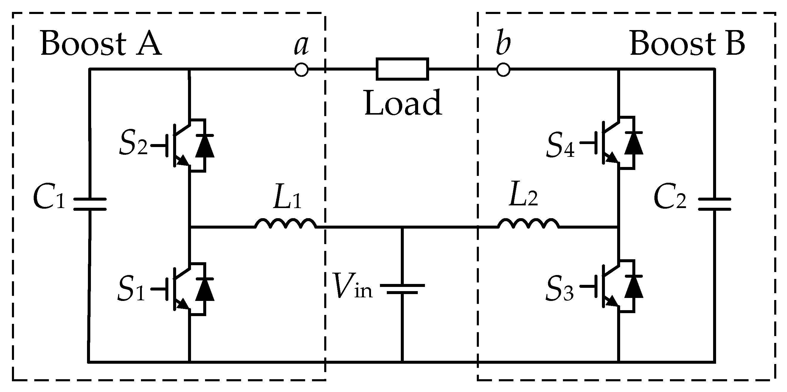
The topology of the differential boost inverter studied in this article is shown in
Figure 1. The topology uses a synchronous rectification structure, replacing the traditional boost converter’s diodes with a half-bridge. The circuit consists of two boost converter modules, A and B. In module A, the switches S
1 and S
2 operate in a complementary manner, with the duty cycle of S
1 denoted as
Da. In module B, the switches S
3 and S
4 operate in a complementary manner, with the duty cycle of S
3 denoted as
Db. The output voltage of boost A is
va and that of boost B is
vb. The voltage
vo supplied to the load is the difference between the two, as shown in Equation (1). The principle of the differential boost inverter involves controlling the voltage difference between
va and
vb by adjusting the output gain of the two boost circuits to achieve the AC output. The AC component of the output remains unipolar relative to the input-side reference voltage, with
va and
vb containing common-mode voltage. The differential output is used to achieve a bipolar AC output.
We assume that the target output is an AC sinusoidal voltage with a peak value
Vp and a frequency
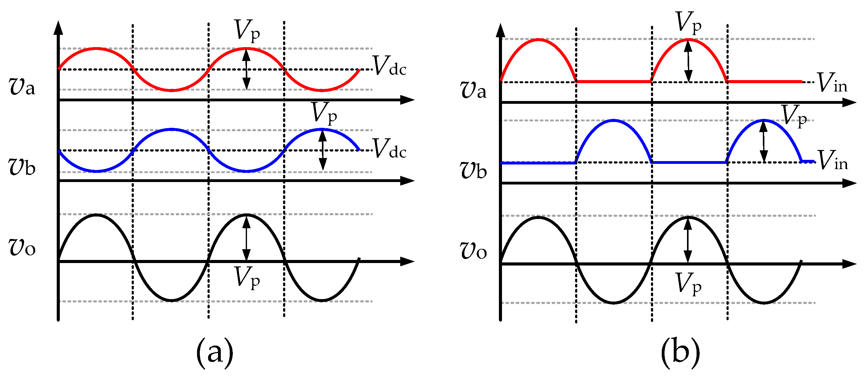
fn. The typical modulation methods of two boost converters that are independently controlled are shown in
Figure 2.
Figure 2a illustrates a dual-sine modulation. Each converter independently controls
va and
vb to be sinusoidal voltages with a peak value of 0.5
Vp, a DC offset
Vdc, and a phase difference of 180°. The resulting combined output is a sinusoidal voltage
vo with a peak value of
Vp. The DC offset voltage
Vdc must ensure that the minimum value of the sinusoid remains positive, requiring
Vdc > 0.5
Vp. Additionally, the duty cycle limits must be considered. The average common-mode voltage
Vcom is
Vdc, and the minimum single-sided output voltage
Vmin is
Vdc − 0.5
Vp. In this mode, the output voltage depends on both the peak values of the two sides and the DC offset voltage, making the adjustment process relatively complex.
Figure 2b depicts the half-cycle modulation. In this method, the two sets of boost converters alternately independently output half-cycle sinusoidal waves and combine them to form a complete sinusoidal voltage. During the phase where chopping is not performed, either S
2 or S
4 remains continuously conducting, and the single-sided output voltage equals
vin. The average common-mode voltage is
Vdc +
Vp/2, and the minimum single-sided output voltage is
Vdc. Half-cycle modulation offers significant advantages. Each set of switches operates for only half a cycle, effectively reducing switch losses. The common-mode voltage is theoretically minimized for boost circuit outputs. However, in practical operation, switching between the PWM mode and the continuous conduction mode can cause oscillations in the output due to the parasitic parameters of the circuit, thereby affecting the AC-side harmonics.
The modulation schemes described above treat the two boost converters as independent control entities without interdependent duty cycles. Alternatively, following a traditional inverter modulation method, where the bridge arms of the two converters complementarily operate, can also be applied to differential boost inverters, simplifying the duty cycle calculations. The AC gain of differential boost inverters can be defined as
Zo. According to the gain formula of the boost converter,
Zo is calculated as shown in Equation (2).
In the formula, when
Da >
Db, the gain is positive; when
Da <
Db, the gain is negative; and when
Da =
Db, the gain is zero. Thus, the output gain curve is symmetrically distributed around the 0.5 duty cycle. As shown in
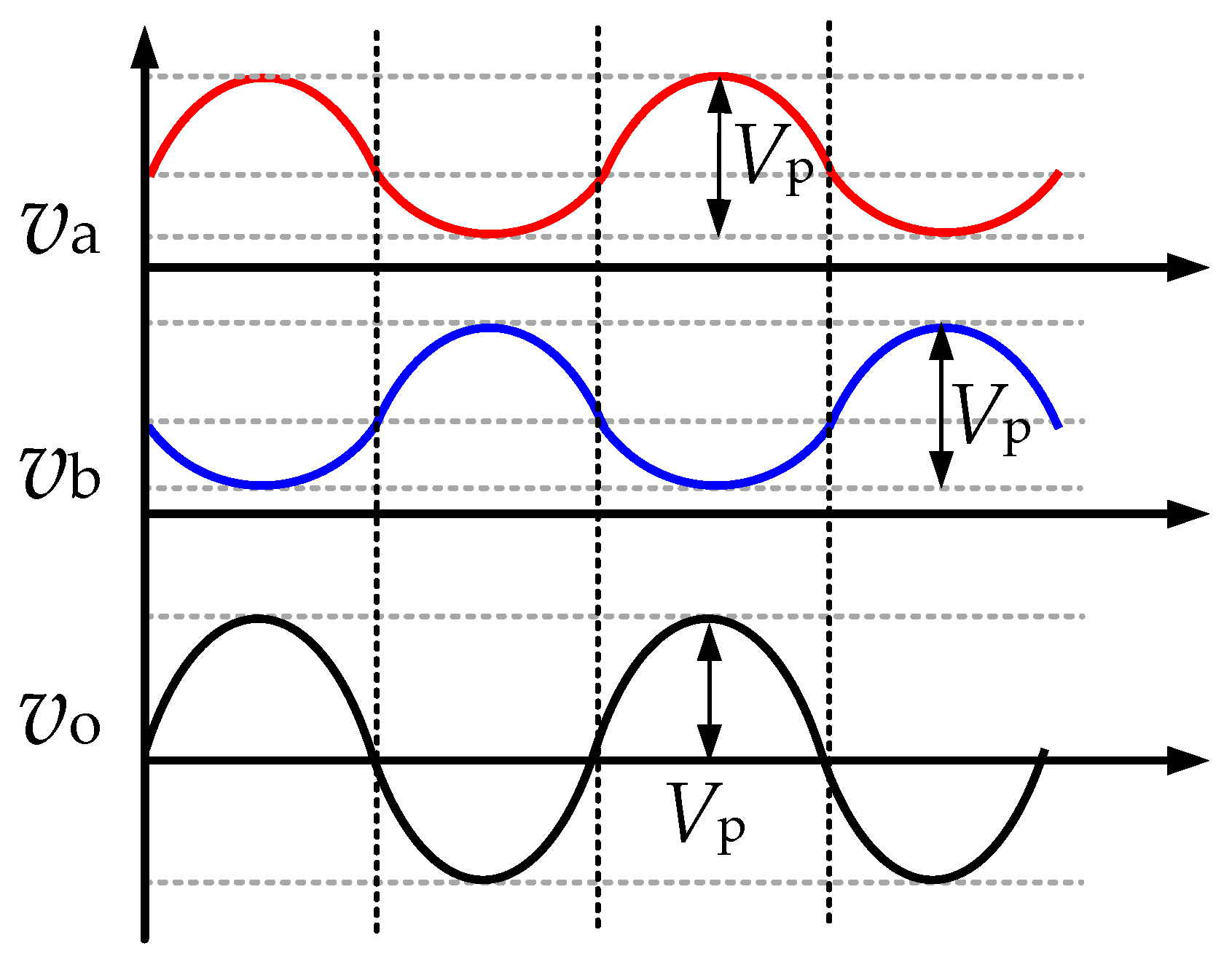
Figure 3, due to the nonlinear relationship between the boost converter’s gain and the duty cycle, the single-sided output voltages
va and
vb are not sinusoidal. Given that
Da and
Db satisfy Equation (3), if the duty cycle corresponding to the peak voltage
Vp is
Dp, then the minimum single-sided output voltage is expressed by Equation (4). In this case, the common-mode voltage will vary with the output. When the duty cycle is 0.5, the average common-mode voltage is 2
Vin.
3. Flexible Common-Mode Voltage Modulation for Differential Boost Inverters
When the differential boost inverter outputs the same voltage on both sides, this is defined as the zero point of the output. In the symmetrical modulation method, the zero point occurs when both converters output a 50% duty cycle, and the sum of the duty cycles remains 1. Based on this, if the voltage and duty cycle corresponding to the zero point are changed, the slope of the gain curve and the symmetry center also change, allowing the same AC output to be achieved under different common-mode voltages.
This article proposes a modulation method for differential boost inverters with a flexible common-mode voltage (FCV). This method optimizes the common-mode voltage by adjusting the gain characteristics through altering the voltage corresponding to the zero point. First, the duty cycle calculation formula for this modulation method is derived. The operating point
T can be defined as the sum of the duty cycles of module A and module B as Equation (5).
In the operation of inverters, factors like dead time and boost range limitations impose constraints on the duty cycle. We denote the upper and lower limits of the duty cycle as
Dmin and
Dmax, respectively. Therefore,
Da and
Db must satisfy Equation (6). Similarly, the range for
T, which is the sum of
Da and
Db, should satisfy Equation (7).
When T > 1, the duty cycle should satisfy Equation (8).
When T < 1, the duty cycle should satisfy Equation (9).
Substituting Equation (5) into Equation (2) yields Equation (10).
Equation (10) is rearranged into an equation involving
Da and gives Equation (11).
Solving Equation (11) yields Equation (12), which can be used to calculate the duty cycle
Da based on the gain
Zo.
When
T = 1 and module 1 and module 2 complement each other in conduction, the converter operates under traditional symmetric modulation. At this point, the relationship between the duty cycle and the gain is as shown in Equation (13).
Specifically, from Equations (5) and (10), it follows that, when D1 = D2 = T/2, Zo = 0. This means that, when the duty cycles of the two converters are equal, the output voltage at the load end is 0.
The reference signal for sinusoidal modulation is defined as Equation (14).
In the equation,
Zm represents the ratio of the peak AC output voltage to the input DC voltage, and
ω is the angular frequency. Therefore, the relationship describing the variation in the duty cycle over time is Equation (15).
It should be noted that, when
T < 1, the relationship between
Zm and
T must satisfy Equation (16).
Figure 4 is a modulation block diagram of the drive signal based on Equation (15). In the figure, the input signal is
Zmsin(
ωt), and the calculated duty cycles
Da and
Db generate PWM drive signals through comparison with a triangular wave at the switching frequency, driving the operation of the switchers.
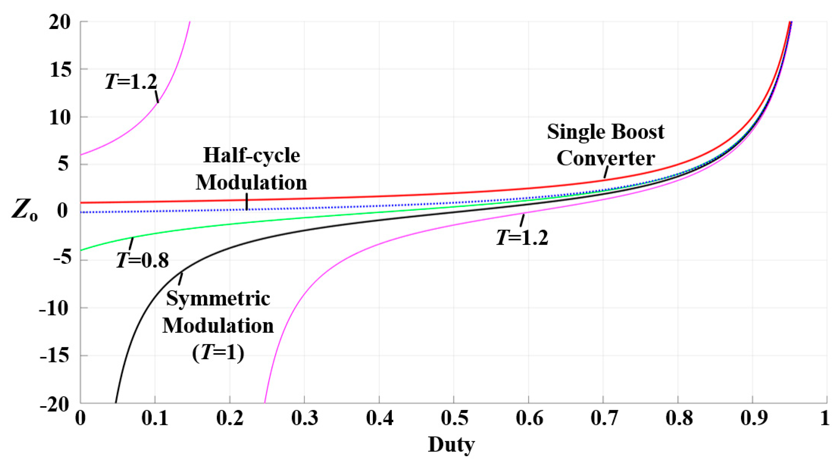
According to the gain calculation formulas for different modulation methods, the gain versus duty cycle curves are plotted as shown in
Figure 5.
Figure 5 includes the gain curves of the boost converter and the differential boost inverter under symmetric modulation (
T = 1), half-cycle modulation, FCV modulation (
T = 0.8), and FCV modulation (
T = 1.2). In the case of half-cycle modulation, since each converter is independently modulated, only the positive gain curve is shown. The negative gain curve is symmetrically centered around it.
As shown in
Figure 5, the gain of the boost converter increases nonlinearly with the duty cycle. The larger the duty cycle, the faster the gain rises. When the gain rises too rapidly, slight disturbances in the duty cycle can cause significant variations in gain, which is detrimental to control stability. Therefore, the boost converter has limitations in its voltage boosting range. The gain curve of half-cycle modulation is equivalent to the boost gain curve shifted downwards by
Vin. Below a duty cycle of 0.5, the gain changes minimally. As the duty cycle increases, the rate of gain change markedly rises, entering the effective voltage regulation region. However, as the duty cycle approaches 1, the gain curve of half-cycle modulation tends to overlap with that of the boost converter.
The gain curve of traditional symmetric modulation exhibits a symmetric shape around a duty cycle of 0.5, where the AC gain is 0 and the single-side voltage gain is 2 at a duty cycle of 0.5. Within the commonly used gain range, modulation operates around 0.5, and the duty cycle does not reach 0. When using FCV modulation, the gain curve shows significant differences compared to symmetric modulation. When T > 1, the gain curve becomes hyperbolic. For example, at T = 1.2, the gain curve is divided into two curves with 0.2 as the boundary. However, since duty cycles greater than 1 do not exist, the left curve is invalid. The right-side gain curve is symmetrically centered around T/2. At T = 1.2, the symmetric center duty cycle is 0.6, corresponding to a single-side voltage gain of 2.5, which results in a higher average common-mode voltage compared to symmetric modulation. As the duty cycle approaches 1, the gain curve also tends to overlap with the boost converter gain curve.
When T < 1, the adjustment range of the gain and duty cycle is compressed, and the gain curve becomes limited segments. At T = 0.8, the symmetric center duty cycle is 0.4, corresponding to a single-side voltage gain of approximately 1.67. At this point, the maximum duty cycle is 0.8, corresponding to a gain of 4. Unlike symmetric modulation, a duty cycle of 0 can be involved in modulation, corresponding to a gain of −4. When T < 1, due to the reduction in gain at the symmetric point and the use of 0 duty cycle in modulation, the average common-mode voltage component can be effectively reduced, and the calculation of the duty cycle is simplified. This method is more suitable for situations with lower boost ratios.
4. Simulations and Experiments
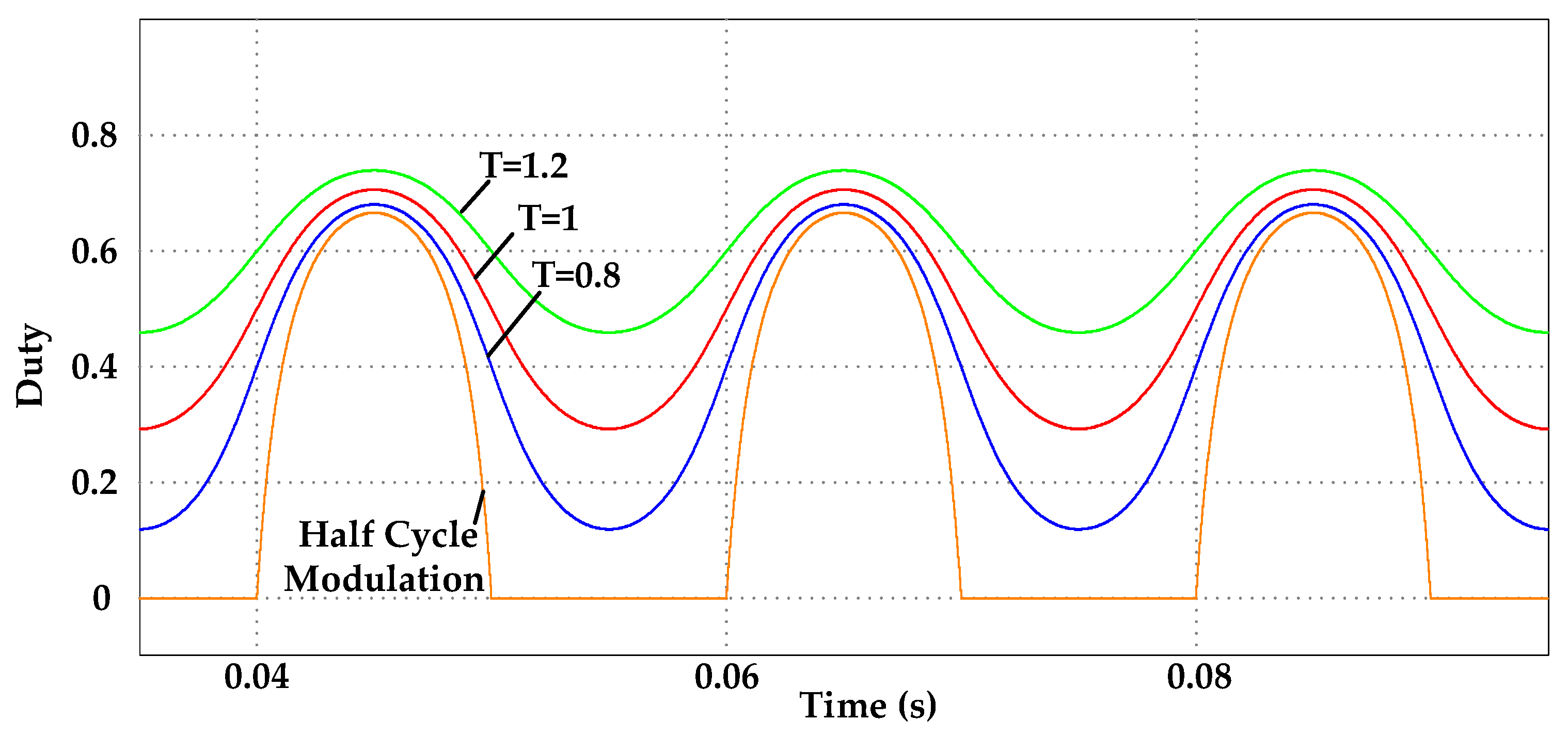
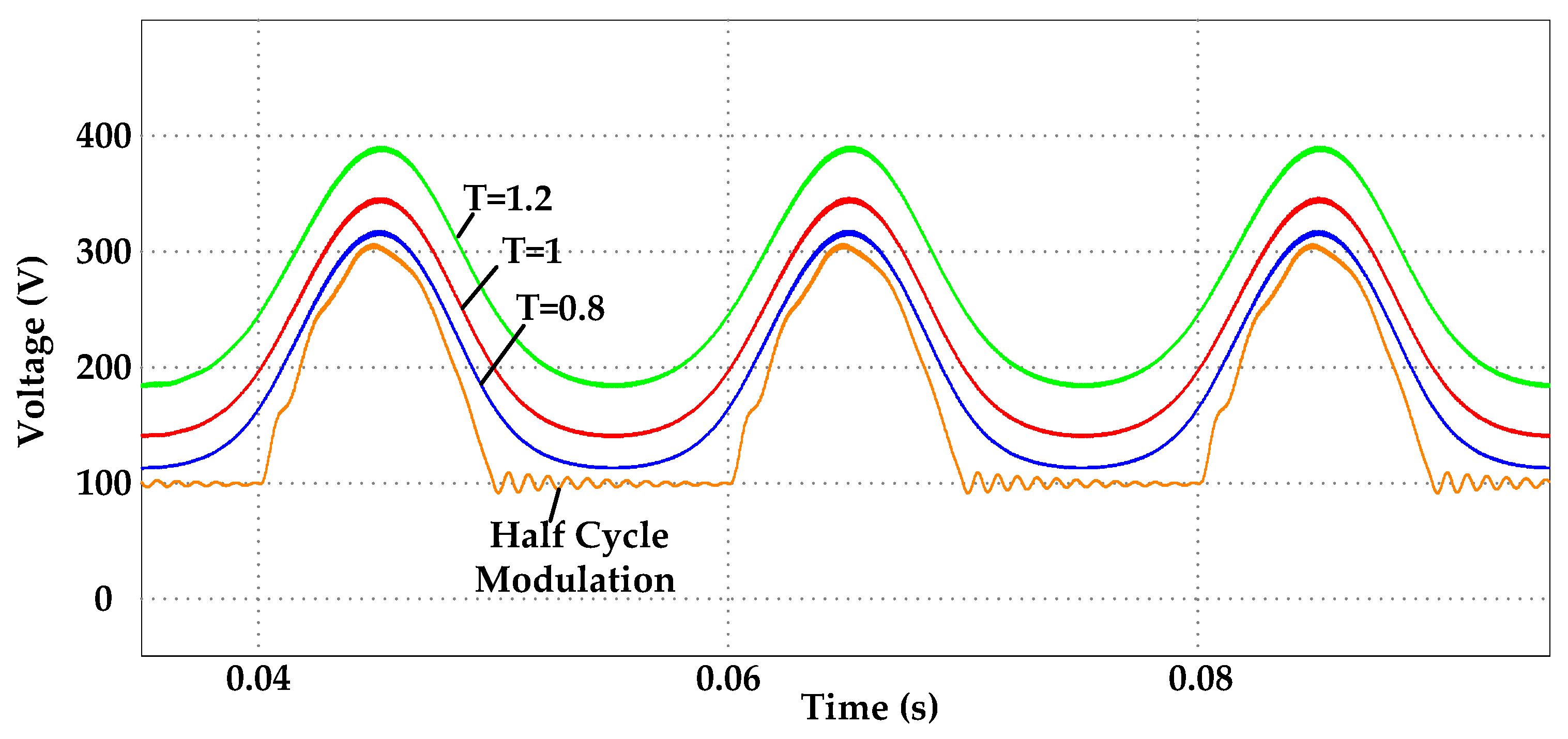
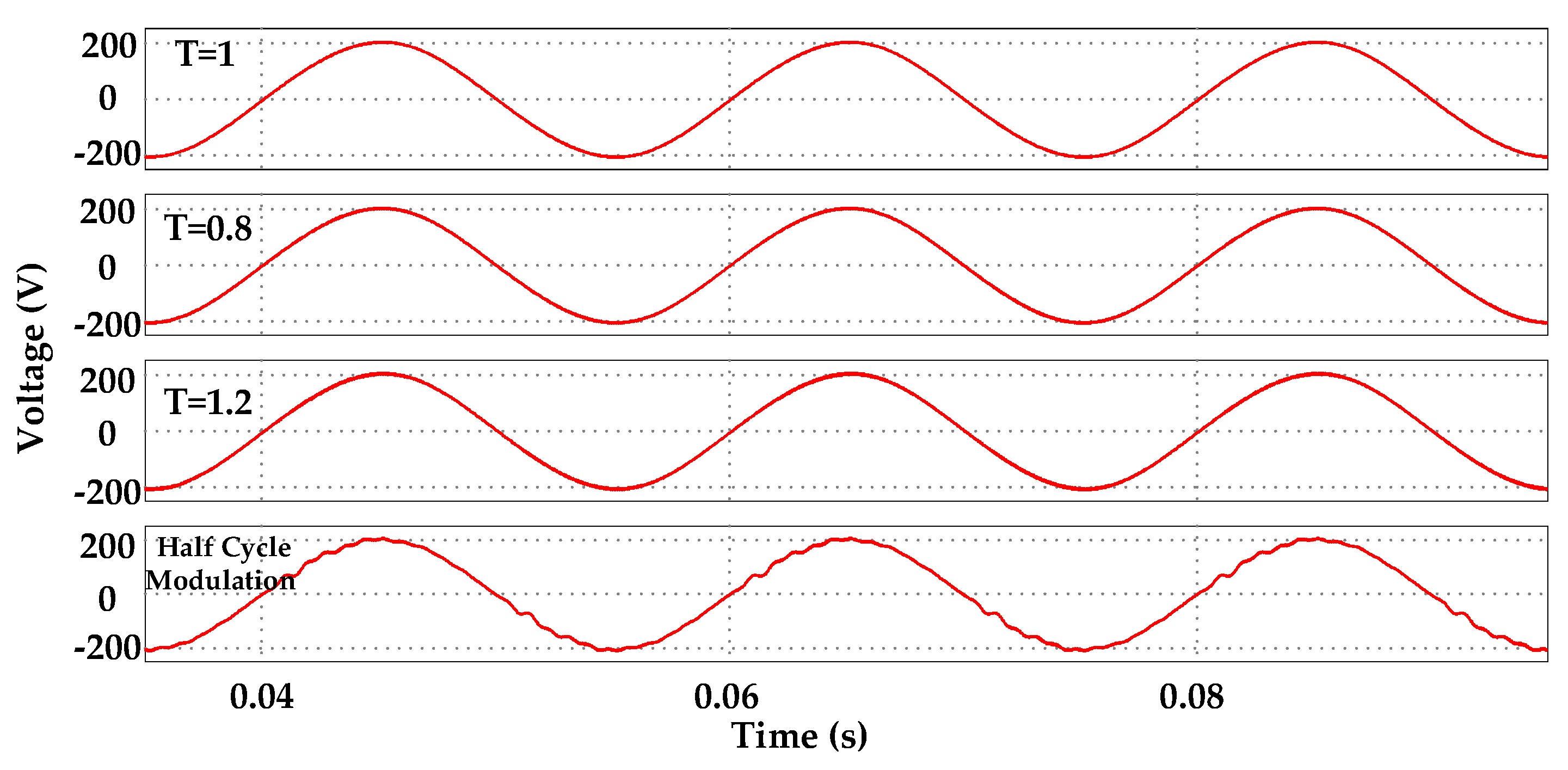
To verify the advantages of the proposed modulation method, simulation and experimental validations were conducted. First, the simulation parameters are introduced below. The input DC voltage was 100 V. The boost converters on both sides used the same inductors and capacitors, with inductance values of 400 μH and capacitance values of 50 μF. The load was 10 Ω, the switching frequency was 20 kHz, and the target peak output voltage was 200 V at 50 Hz, which corresponded to an AC gain setting of 2. To verify the proposed FCV modulation method, working points of T = 0.8 and T = 1.2 were selected and compared with half-cycle modulation and symmetric modulation (T = 1).
Figure 6,
Figure 7 and
Figure 8 show the simulation waveforms.
Figure 6 displays the duty cycle waveforms for half-cycle modulation, symmetric modulation, and the proposed FCV modulation method.
Figure 7 shows the corresponding single-side output voltage waveforms, and
Figure 8 shows the output AC voltage waveforms under different modulation methods. From
Figure 6 and
Figure 7, it can be observed that the sinusoidal duty cycle results in a voltage that is no longer a regular sinusoidal curve due to the nonlinearity of the gain curve. The standard sinusoidal output voltage is obtained by synthesizing the two non-sinusoidal curves, as shown in
Figure 8. As the operating point
T decreases, the duty cycle signal of FCV modulation gradually approaches half-cycle modulation, effectively reducing common-mode voltage. Additionally,
Figure 7 shows that noticeable oscillations can be observed in the single-side voltage after two transitions between the half sinusoidal output period and the pass-through period in half-cycle modulation, which are transferred to the differential voltage. The waveform of FCV modulation is smoother compared to half-cycle modulation, preventing additional system oscillations. Therefore, with the same system parameters, the FCV modulation method exhibits better harmonic performance compared to half-cycle modulation.
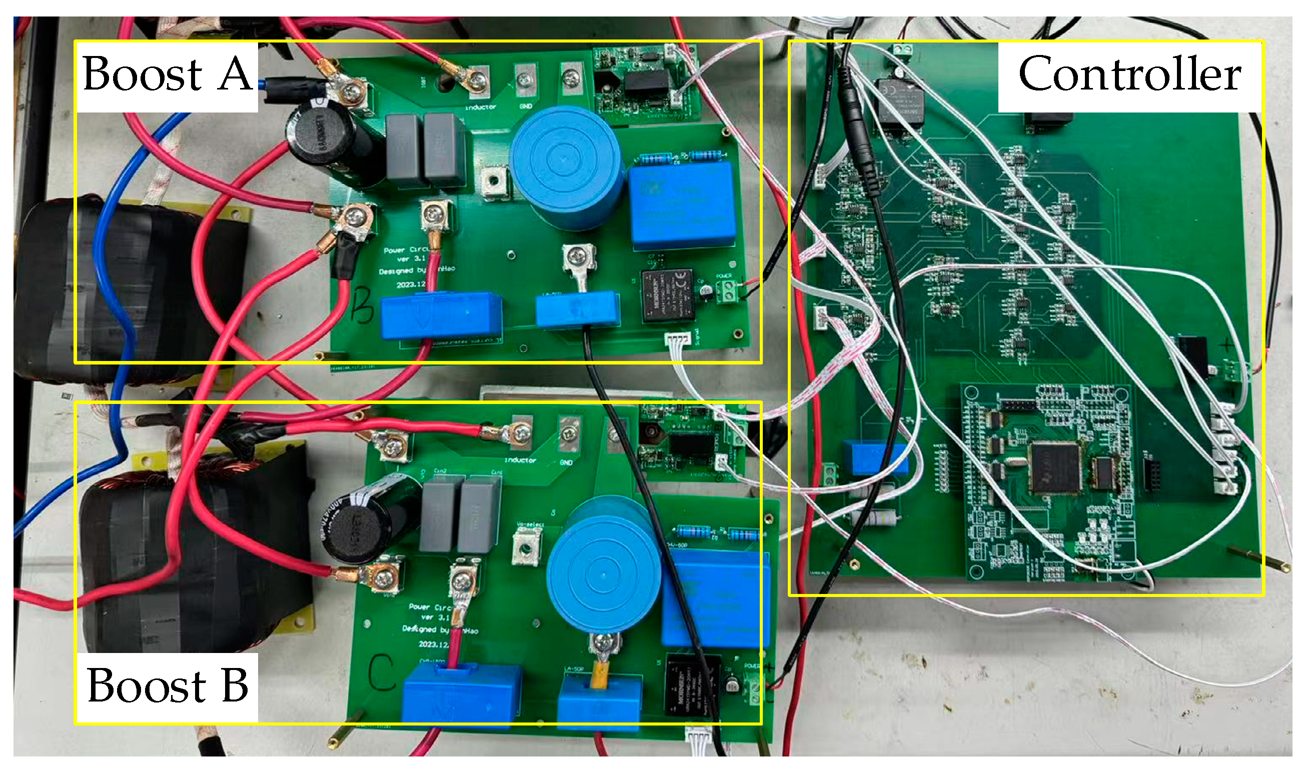
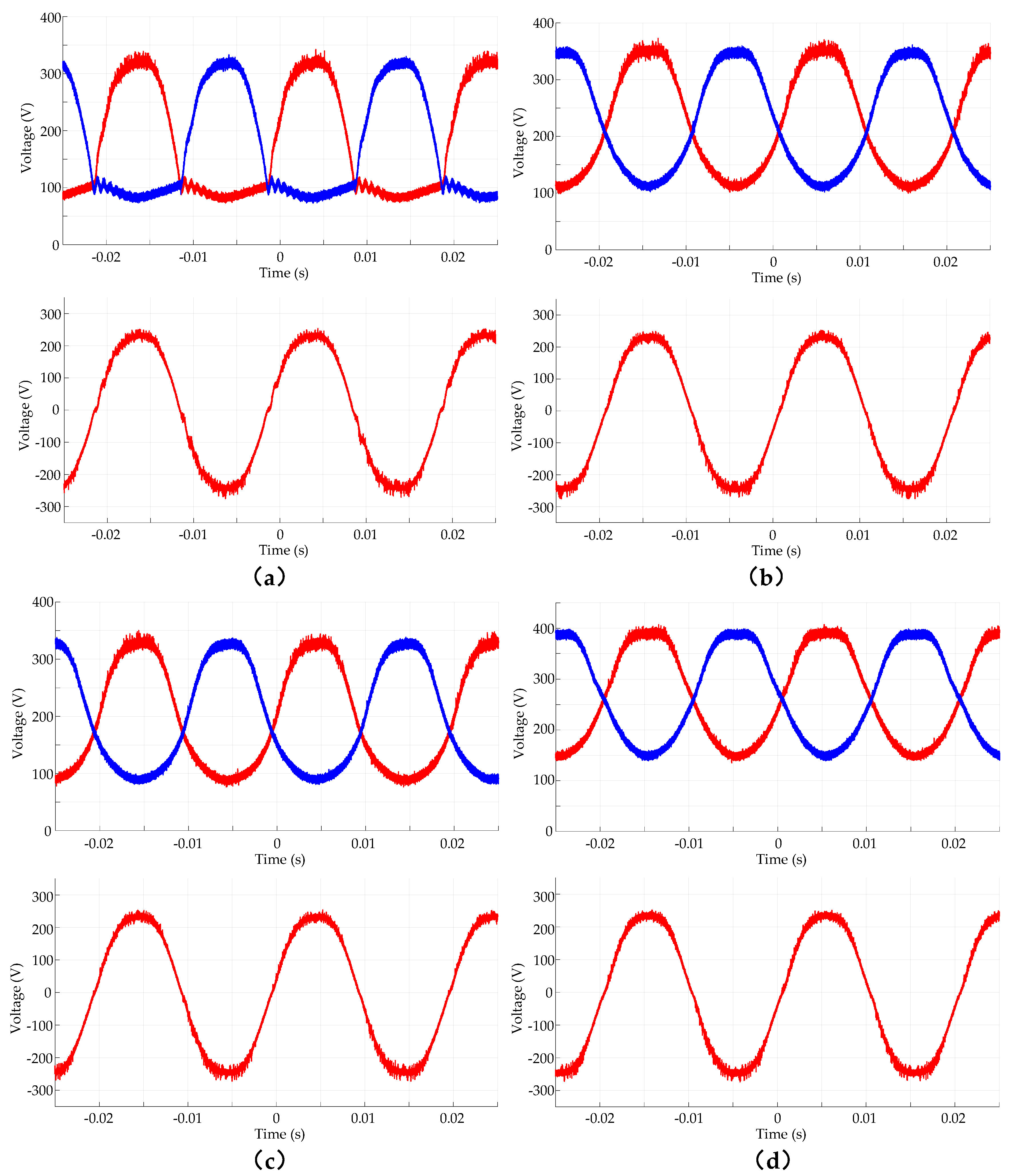
An experimental platform was also set up to compare various modulation methods. The differential boost inverter setup is shown in
Figure 9. The circuit parameters are essentially the same as those used in the simulation, which are shown in
Table 1. The inductance value is 400 μH, the capacitance value is 50 μF, and the load resistance is 48 Ω. The switching frequency is set to 20 kHz. The input DC voltage is 96 V, and the actual root mean square (RMS) value of the output AC voltage is 180 V, with a peak value of approximately 230 V at a frequency of 50 Hz.
Figure 10 shows the single-side output voltage and differential output voltage waveforms of the differential boost inverter under different modulation methods.
Figure 10a represents half-cycle modulation,
Figure 10b represents symmetric modulation (
T = 1),
Figure 10c represents FCV modulation (
T = 0.8), and
Figure 10d represents FCV modulation (
T = 1.2). The output voltage waveforms of the four modulation methods are essentially the same, with a peak value of approximately 230 V. For half-cycle modulation, the minimum single-sided voltage fluctuates around 100 V, with a peak value of about 320 V. For symmetric modulation, the minimum single-sided voltage is about 110 V, with a peak value of around 350 V. For FCV modulation (
T = 0.8), the minimum single-sided voltage is about 90 V, with a peak value of approximately 327 V. For FCV modulation (
T = 1.2), the minimum single-sided voltage is around 150 V, with a peak value of about 390 V. A comparison reveals that, for the same output voltage under the same AC gain, the single-side voltage at
T = 0.8 are significantly lower than at
T = 1 and
T = 1.2, approaching the level seen in half-cycle modulation. Additionally, oscillations can be observed in the half-cycle modulation waveform. The FFT analysis of the output voltage, shown in
Table 2, indicates that symmetric modulation and FCV modulation perform similarly and better than half-cycle modulation.
From the simulation and the experimental data, it can be concluded that, by appropriately reducing the value of
T, FCV modulation can effectively lower the common-mode voltage and provide a better output power quality compared to half-cycle modulation. However, it is worth noting that this also reduces the range of the gain curve, making it more suitable for applications with lower boost ratio requirements. When the boost ratio is too high, as seen in
Figure 10d, the output waveform exhibits a flat-top phenomenon, which affects the output quality.
