Article

Breakdown Characteristics of Schottky Barrier Diodes Used as Bypass Diodes in Photovoltaic Modules under Lightning Surges

1
Faculty of Engineering, Osaka Electro-Communication University, 18-8 Hatsucho, Neyagawa 572-0833, Japan
2
National Institute of Technology, Ube College, 2-14-1 Tokiwadai, Ube 755-8555, Japan
3
National Institute of Technology, Yonago College, 4448 Hikonacho, Yonago 683-0854, Japan
4
National Institute of Technology, Oshima College, 1091-1 Komatsu, Suo-Oshimacho 742-2106, Japan
5
National Institute of Technology, Tsuyama College, 624-1 Numa, Tsuyama 708-0824, Japan
*
Author to whom correspondence should be addressed.
Energies 2023, 16(23), 7792; https://doi.org/10.3390/en16237792
Submission received: 24 October 2023 / Revised: 19 November 2023 / Accepted: 24 November 2023 / Published: 27 November 2023
(This article belongs to the Special Issue Photovoltaic Solar Cells and Systems: Fundamentals and Applications)

Abstract

:
Damage to photovoltaic power-generation systems by lightning causes the failure of bypass diodes (BPDs) in solar cell modules. Bypass diodes damaged by lightning experience high-resistance open- or short-circuit failures. When a bypass diode experiences short-circuit failure due to indirect lightning, the damage may not be immediately visible. When solar radiation is subsequently received, the current circulating in the closed circuit formed by the cell string and short-circuited bypass diode flows, resulting in overheating and burnout of the short-circuited bypass diode. The authors’ research group previously reported that when a bypass diode fails within a range of approximately 10−1 Ω to 10 Ω, the heat generated by the failed bypass diode is high, posing the risk of burnout. However, the detailed failure characteristics of the bypass diode that fail because of indirect lightning surges are not clear. In this study, we performed indirect lightning fracture tests and clarified the dielectric breakdown characteristics of Schottky barrier diodes (SBDs) contained in the bypass diodes of photovoltaic solar cell modules, which are subjected to indirect lightning surges. Furthermore, we attempted to determine the conditions of indirect lightning that resulted in a higher risk of heat and ignition. As a result, short-circuit failures occurred in all the Schottky barrier diodes that were destroyed in the forward or reverse direction because of the indirect lightning surges. Moreover, the fault resistance decreased as the indirect lightning surge charge increased. These results indicate that the risks of heat generation and burnout increase when the Schottky barrier diode fails with a relatively low electric charge from an indirect lightning surge. In addition, we observed that for a forward breakdown of the Schottky barrier diode, the range of the indirect lightning surge that results in a fault condition with a higher risk of heat generation and burnout is wider than that for a reverse breakdown.

1. Introduction

In recent years, cases of photovoltaic systems (PVSs) being damaged by lightning have been reported, which cause bypass diodes (BPDs) in photovoltaic modules (PV modules) to fail and result in burnout [1,2]. Bypass diodes play a crucial role in reducing power loss due to hotspots and cell string conduction failure when the PV modules are partially shaded. Currently, Schottky barrier diodes (SBDs) are used, which have lower peak inverse voltages than PN junction diodes [3]. These can be damaged by overvoltage from indirect lightning and similar sources [4,5,6]. The damage to PV modules caused by indirect lightning is more extensive than that caused by direct lightning, although the failure is less severe. Furthermore, Schottky barrier diodes damaged by indirect lightning experience high-resistance open failure or short-circuit failure. When a bypass diode experiences short-circuit failure due to indirect lightning, the damage may not be immediately visible. When solar radiation is subsequently received, the current circulates in the closed circuit formed by a cell string, and the short-circuited bypass diode flows, resulting in overheating and burnout of the short-circuited bypass diode [7,8]. The authors’ research group previously reported that when a bypass diode fails within a range of approximately 10−1 Ω to 10 Ω, the heat generated by the failed bypass diode is high, posing the risk of burnout. Furthermore, if a reverse-current blocking diode fails in addition to the bypass diode within a PV array, the inverse current from the sound PV array flows into the short-circuited bypass diode, increasing the risk of heat generation and burnout [9]. Therefore, it is important to ascertain the characteristics of bypass diode failure owing to indirect lightning in mechanisms wherein the bypass diode may generate heat and burnout [10]. However, the detailed failure characteristics of the bypass diode that fail because of indirect lightning surges are not clear.
In this paper, we shall identify the insulation breakdown characteristics of the bypass diodes used in PV modules that have experienced an indirect lightning surge through artificially indirect lightning damage tests and study the conditions for high risk of bypass diodes used in PV modules that generate heat and catch fire owing to indirect lightning.

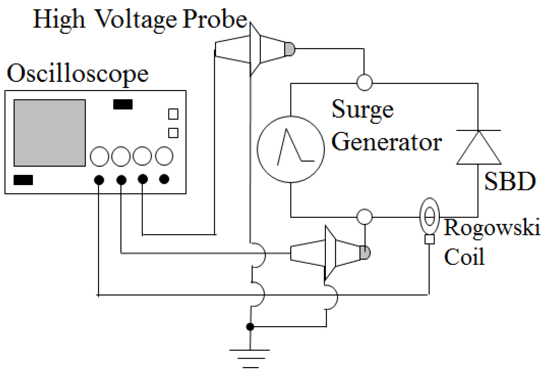
2. Experimental Methods

Figure 1 shows a summary of the Schottky barrier diode lightning surge tests. The lightning impulse current waveform used in this withstand test using lightning is defined in JEC-0202 [11] as the ratio of the virtual front time Tf and virtual time to half-value Tt, Tf/Tt, which is 10/350 μs for a direct lightning strike. Conversely, this ratio is 8/20 μs for indirect lightning; a direct lightning strike has an extremely large energy compared with indirect lightning. Tests on the application of direct lightning current near PV modules and to the metal frames of PV modules have confirmed that indirect lightning can cause the bypass diodes in PV modules to fail [12]. Therefore, in this test, to identify the failure characteristics of bypass diodes due to an artificial indirect lightning surge, we used a combination waveform that was output with a voltage waveform of Tf/Tt = 1.2/50 μs when the test circuit was open and a current waveform of Tf/Tt = 8/20 μs when the test circuit was shorted, according to test standards for artificial indirect lightning surge immunity for electrical devices (IEC 61000-4-5), as shown in Figure 2 [13]. To set the charging value of the indirect lightning surge generator used in this experiment according to the discharge voltage wave front of the indirect lightning surge tester at the time of open circuit opening, we defined this as VSET and applied the combination waveform to a Schottky barrier diode for one cycle. We then computed the difference in the voltage applied to a Schottky barrier diode through ground potential measurements at both ends of the Schottky barrier diode using two high-voltage probes (Iwatsu Electric Co., Ltd., Tokyo, Japan, HV-P30A). The surge current was measured using a Rogowski coil-type current probe (Iwatsu Electric Co., Ltd., SS-289A). The amount of charge of the indirect lightning surge was computed, and its correlation with the impact on the Schottky barrier diode was evaluated. The Schottky barrier diode (FSQ30A045, Kyocera Corp., Tokyo, Japan, repetitive peak reverse voltage 45 V, average rectified current 30 A) used in testing was manufactured and had the same specifications as the one loaded into the PV module, which underwent burnout failure from indirect lightning damage. We then measured and evaluated the current–voltage characteristics of the indirect lightning surge-tested Schottky barrier diode in the source measurement units (Keysight Technologies, Inc., Tokyo, Japan, B2901A).

3. Experimental Results

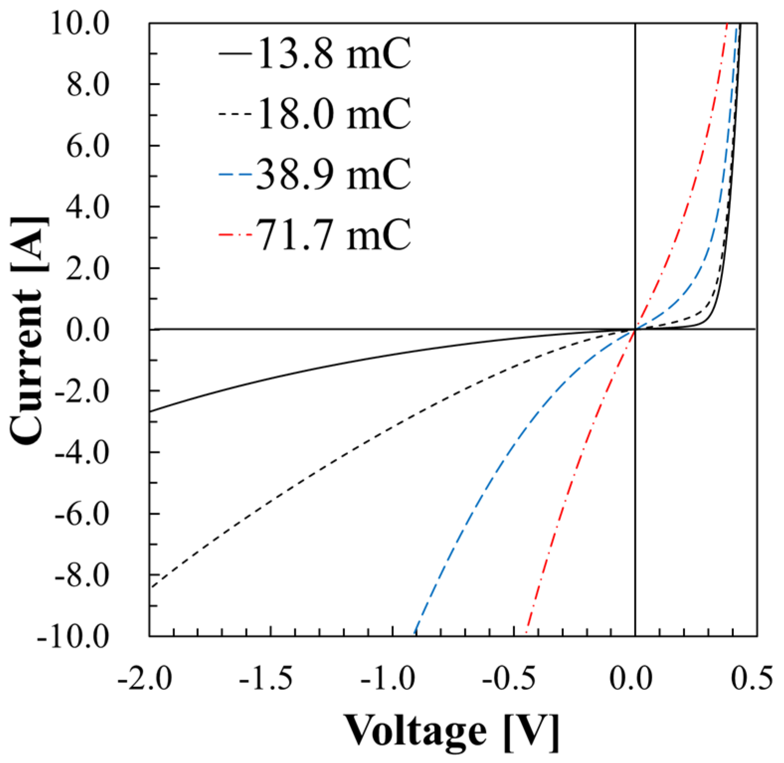
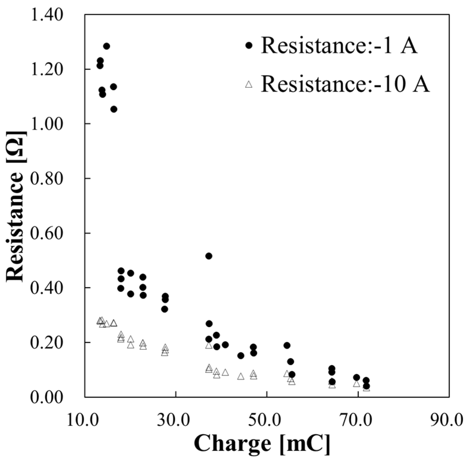
3.1. Indirect Lightning Surge Reverse Stress Test for Bypass Diode (BPD)

We conducted tests by applying an indirect lightning surge in the reverse direction to a Schottky barrier diode used as a bypass diode in a PV module. Figure 3 shows the current–voltage characteristics of the tested Schottky barrier diode. To set the charging for the output of the indirect lightning surge tester used during testing using the voltage wave front value (VSET) at the time of an open circuit, we computed and evaluated the electric charge Qs [mC] of the indirect lightning surge from the surge current waveform flowing into the Schottky barrier diode with each VSET. As shown in Figure 3, a short-circuit failure in the Schottky barrier diode was confirmed when an indirect lightning surge of Qs = 0.502 mC or higher was applied. Furthermore, forward diode voltage start-up can be confirmed for the failed Schottky barrier diode with a surge in Qs. However, current flow and short circuit were confirmed for the reverse characteristics. In a Schottky barrier diode, when a high electrical field is applied in the reverse direction, the electrons within the Schottky barrier diode accelerate because of the high electrical field and collide with the semiconductor crystal lattice, thereby exciting the valence band electrons into conduction electrons. With multiple repeated applications, the current flows in the reverse direction (electron avalanche yield). Consequently, we conclude that when a sufficient potential difference (electric field) is provided within the element to cause an electron avalanche yield, a large current flows within the element, resulting in heat generation, melting, and the loss of the Schottky barrier diode Schottky junction, and eventual short-circuit failure. In addition, as Qs increases, the failure resistance value decreases, approaching the linear current–voltage characteristics. However, because diode characteristics can also be confirmed at Qs = 4.70 mC or less, the Schottky junction loss region is only partial.
Figure 4 shows the relationship between the failure resistance value and indirect lightning surge charge of a tested Schottky barrier diode with an indirect lightning surge applied in the reverse direction. The failure resistance value, accounting for the range of PV module operating current, exhibited a resistance value at operating current values of −1 A and −10 A. In addition, Schottky barrier diode breakdown is influenced by the indirect lightning surge energy. Hence, we evaluated it in terms of Qs and failure resistance characteristics. Figure 4 also reveals that a larger Qs results in a lower Schottky barrier diode failure resistance value. When Qs is larger, more heat is generated within the Schottky barrier diode, owing to the indirect lightning surge application, and a higher range of Schottky barrier diode Schottky junction melting results in a lower failure resistance value. Consequently, if the Schottky barrier diode fails, owing to an indirect lightning surge with a relatively small charge within a range of 0.502 mC to 2.77 mC, then the bypass diode will fail within a range of 10−1 Ω to 10 Ω, which poses a high risk of heat generation and catching fire.

3.2. Indirect Lightning Surge Forward Surge Test for Bypass Diodes (BPDs)

We conducted tests with the forward application of an indirect lightning surge to a Schottky barrier diode. Figure 5 shows the current–voltage characteristics of the tested Schottky barrier diode. The same figure confirms that the Schottky barrier diode experiences short-circuit failure with an indirect lightning surge strike of Qs = 13.8 mC or higher. During the forward breakdown of the Schottky barrier diode, heat was generated within the Schottky barrier diode, depending on the forward voltage drop and the passing indirect lightning surge current. When the aforementioned indirect lightning surge current increased, the Schottky junction region of the Schottky barrier diode melted, owing to heat generation. In addition, we observed that in the measurement range, as Qs increased, the Schottky barrier diode voltage–current characteristics approached linear resistance characteristics, and the slope gradually increased.
Figure 6 shows the relationship between the failure resistance value and the indirect lightning surge charge of a tested Schottky barrier diode with an indirect lightning surge applied in the forward direction. As shown in the figure, a larger indirect lightning surge Qs decreased the failure resistance value of the Schottky barrier diode, which then approached short-circuit failure. Although the indirect lightning surge was applied to the Schottky barrier diode in the forward direction, similar to the reverse stress, heat generation owing to the surge current increased with increasing Qs, and the Schottky junction melting range increased, thereby decreasing the failure resistance. In addition, in the case of forward breakdown of a Schottky barrier diode owing to an indirect lightning surge, the range of the indirect lightning surge charge that caused failure within a 10−1 Ω to 10 Ω range was observed to be 13.8 mC to 64.3 mC. Furthermore, in the Schottky barrier diode failure due to a forward surge, a failure state with a high risk of burnout is more likely than the failure of the indirect lightning surge in the reverse direction.

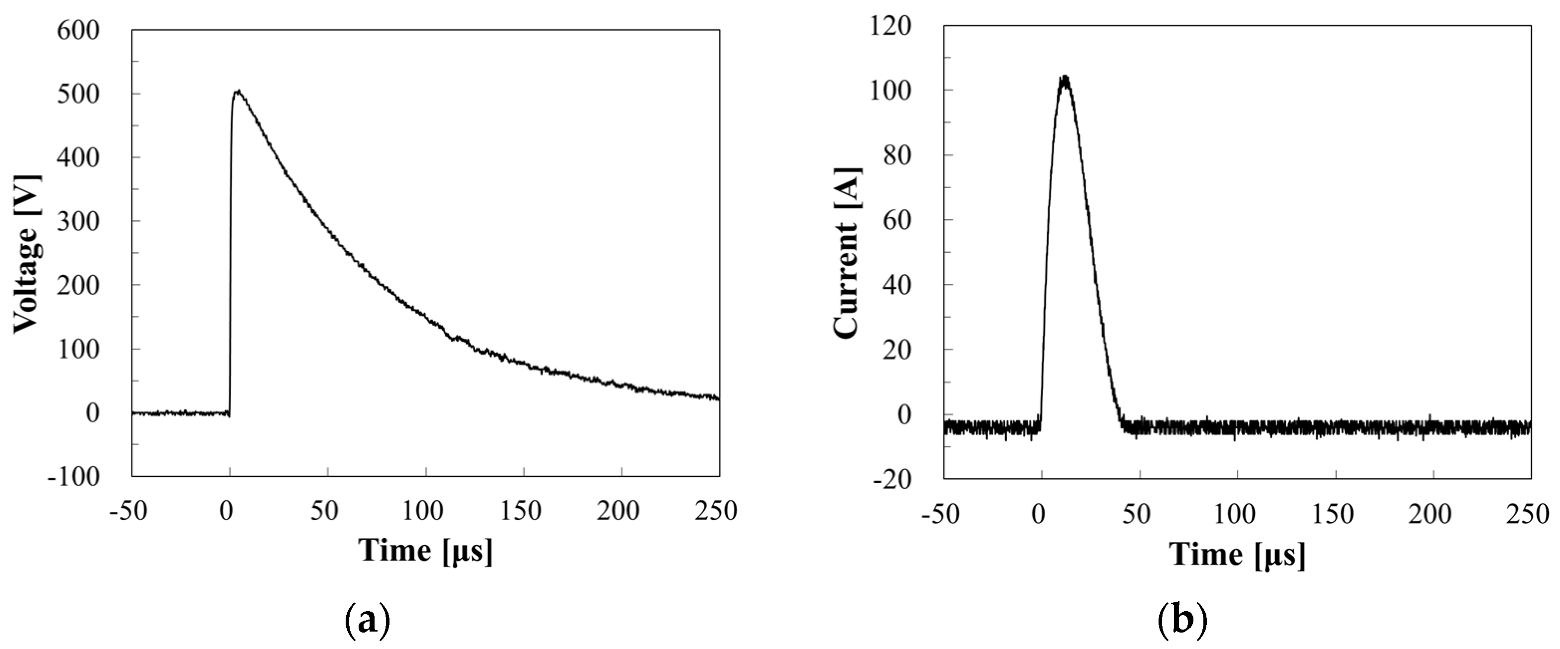
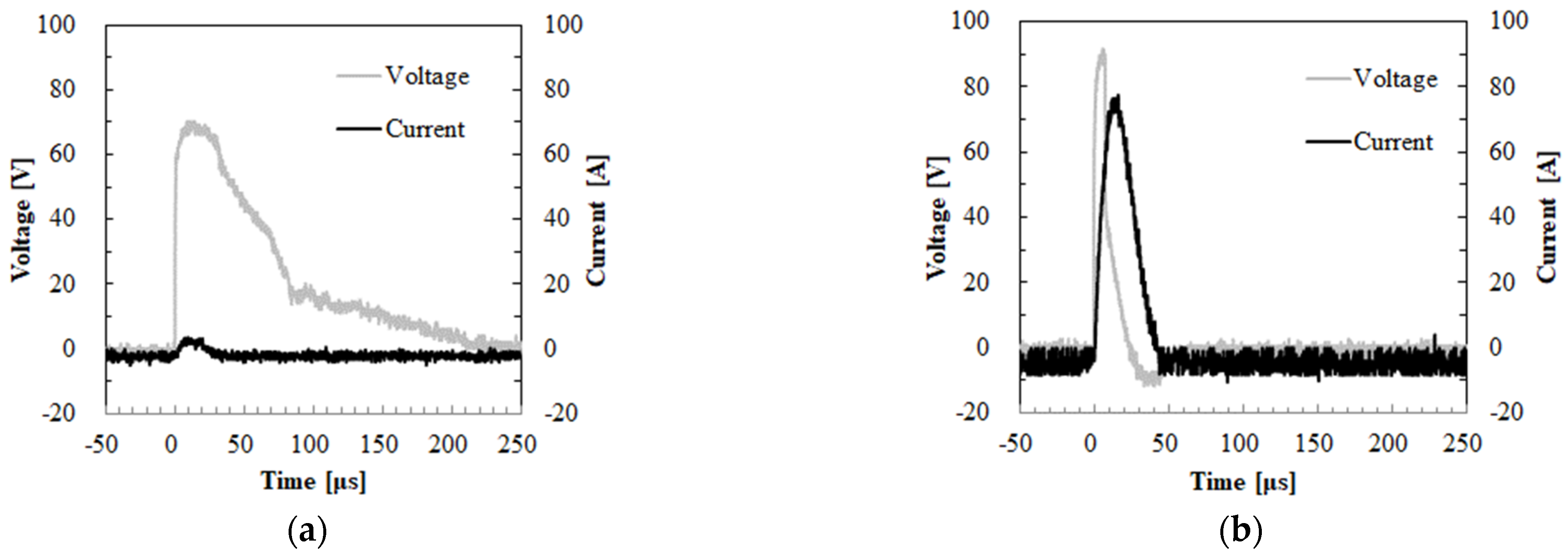
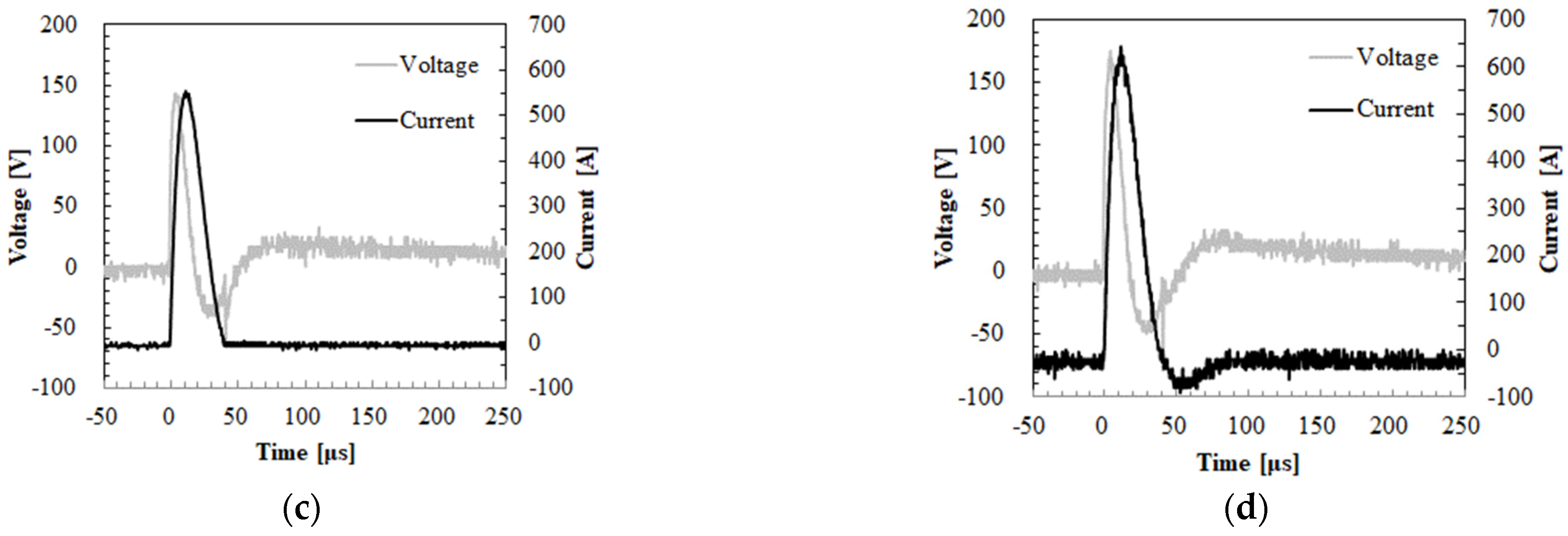
3.3. Schottky Barrier Diode (SBD) Applied Voltage and Current Waveforms in Indirect lightning Surge Tests

Figure 7 shows the current and voltage waveforms when an indirect lightning surge is applied to a Schottky barrier diode at each charging value setting. Because we set charging at the output voltage when an open circuit for the output of the indirect lightning surge tester was used in this test, we defined it as VSET and reported the voltage and current applied at the minimum value of VSET at which the Schottky barrier diode failed and the VSET at which no failure occurred. According to (a) and (b) in the figure, when an indirect lightning surge was applied to the Schottky barrier diode in the reverse direction, the current flowing into the Schottky barrier diode during the application of surge voltage with VSET = 0.1 kV was several amperes and did not result in failure. However, the voltage drastically decreased because of the electron avalanche yield, and the current value increased as the indirect lightning surge voltage increased at VSET = 0.3 kV.
According to Figure 7c,d, when an indirect lightning surge was applied to the Schottky barrier diode in the forward direction, the surge current passed through the Schottky barrier diode with a wave height of approximately 550 A at VSET = 2.5 kV and a wave height of approximately 650 A at VSET = 2.9 kV. In addition, in the voltage waveform, the reverse-direction current flow to the Schottky barrier diode at VSET = 2.9 kV was close to t = 50 μs when a reverse bias voltage was applied to the Schottky barrier diode. This was caused by the internal short-circuit failure in the Schottky barrier diode as the excess surge current passed through the Schottky barrier diode in the forward direction.

4. Discussion

We conducted indirect lightning surge tests on a Schottky barrier diode used as a bypass diode in PV modules to identify the mechanism of failure and burnout of bypass diodes within PV modules when damaged by indirect lightning. Based on the results, when the amount of charge of an indirect lightning surge applied to the Schottky barrier diode in both the forward indirect lightning surge and reverse indirect lightning surge tests exceeded a constant value, the Schottky barrier diode experienced short-circuit failure. In addition, the failure resistance value decreased as the indirect lightning surge charge increased. Furthermore, we observed that the amount of heat generated increased when the bypass diode failed between 10−1 Ω and 101 Ω [8]. Based on the results of these tests, when the bypass diode failed owing to an indirect lightning surge with a relatively small charge, the failure was within a range of resistance values, with a high risk of heat generation and burnout. In addition, the range of indirect lightning surge charge within which failure occurred with a failure resistance value range of 10−1 Ω to 10 Ω was wide, and compared with when an indirect lightning surge was applied in the reverse direction, the Schottky barrier diodes were likely to reach failure mode with a high possibility of burnout. The failure modes of the bypass diode turn out to be short-circuit failure and open failure [7,8]. In these tests, all failed bypass diodes were characterized by short-circuit failures, and no Schottky barrier diode experienced an open-circuit failure. The cause of open failure in the bypass diode is thought to be the presence of a process that increases breakdown or short-circuit failure due to the indirect lightning surge of a charge transition to open failure. The latter process is considered to be the bypass diode transitioning to open failure due to the heat generated by the circulating current within a bypass circuit due to bypass diode short-circuit failure or heat generation and burnout by a bypass diode due to reverse current from a sound module string owing to simultaneous short-circuit failure of a reverse-current blocking diode and bypass diode. When a bypass diode experiences short-circuit failure, the output voltage of the module string holding the PV module in which the bypass diode experiences short-circuit failure decreases compared with a sound string. Furthermore, if a voltage difference occurs between the sound module and module string with bypass diode failure when a reverse-current blocking diode is intended to prevent current reversal from experiencing short-circuit mode failure, a reverse current is produced in the string with bypass diode failure. The aforementioned heat-generation process involves a reverse current that is notably larger than that regularly generated in a short-circuited bypass diode. Therefore, attention should be given to the high risk of bypass diode burnout [10]. Effective measures for such reverse currents include installing fuses, not just reverse-current blocking diodes.
The Schottky barrier diode is considered to have failed after the indirect lightning surge stress owing to the heat generated when the surge current passes through the bypass diode elements, regardless of whether it is involved in the forward or reverse stress indirect lightning surges. Figure 8 shows a cross-sectional scanning electron microscopy (SEM) image of a regular Schottky barrier diode, and Figure 9 and Figure 10 show cross-sectional SEM images of the Schottky barrier diode after the indirect lightning surge tests. According to Figure 8, the Schottky barrier diode used in tests had a metal layer with a film thickness of approximately 1 μm, owing to the formation of a Schottky contact on the surface of Si used as the semiconductor. According to the energy-dispersive X-ray spectroscopy (EDX) analysis, we observed that the aforementioned metal layer was formed for Al and Ni. Additionally, Schottky barrier diode elements have junction structures with metal electrodes and solder materials. Figure 9 shows a cross-sectional SEM image of a short-circuited Schottky barrier diode after an indirect lightning surge of charge Qs = 0.934 mC was applied in the reverse direction, with a failure resistance under a reverse direction 1 A current of 0.22 Ω. Conversely, the Schottky barrier diode shown in Figure 10 had an indirect lightning surge of Qs = 29.5 mC applied in the reverse direction, and the failure resistance value was 0.005 Ω. Figure 9a and Figure 10b confirm that the open-package surface of the short-circuited Schottky barrier diode had traces of partially molten solder material from the heat generated by passing through the indirect lightning surge current. A cross-sectional SEM image (Figure 9b–d and Figure 10b–d) of the region containing the melting traces (red-lined area in the image) confirmed the melting of the Al–Ni alloy layer and Si material-forming solder and a Schottky junction. In addition, the melting region expanded proportionally as the charge Qs of the indirect lightning surge increased, and we can confirm that at Qs = 29.5 mC, the metal layer and semiconductor layers melted from the anode to the cathode (Figure 10d). In addition, in the melting region, a region of partial melting and loss of the Schottky junction was formed by the Si and Al–Ni alloys, and the solder material melted. Thus, the Schottky contact was considered to be lost in the melted region, resulting in a short-circuit failure. As shown in Figure 9d, when Qs was small, the metal/semiconductor layer melted primarily around the ends of the region where the solder material was present on the anode electrode side. Conversely, no changes were observed in the sound Schottky barrier diode other than in the confirmed melting region. Consequently, with the Schottky barrier diode that short-circuited owing to an indirect lightning surge, the Schottky barrier junction regions that did not melt had diode characteristics, and the current–voltage characteristics of the short-circuited Schottky barrier diodes measured in these tests (Figure 3 and Figure 5) demonstrate the voltage–current characteristics of a diode and resistor connected in parallel. In addition, partial cracks appeared in the silicon material, as shown in Figure 10d,c. Therefore, although not confirmed in these tests, the Schottky barrier diodes are considered to have experienced open-circuit failure when an indirect lightning surge with a charge Qs larger than the test value is applied.
Silicon Schottky barrier diodes are presently widely used as bypass diodes, and an effective countermeasure against bypass diode failure due to indirect lightning surge reverse stress may be to use a device that can achieve a high withstand voltage, such as a PN junction diode, as it has a low (approximately 40 V to 100 V) withstand voltage (breakdown voltage). Therefore, in the future, we will identify the applicability of materials such as silicon carbide Schottky barrier diodes and PN junction diodes, which are more lightning resistant than silicon Schottky barrier diodes, as bypass diodes to reduce the lightning-indirect failures of bypass diodes in solar modules.

5. Conclusions

The findings of this study on destructive testing with indirect lightning surges of Schottky barrier diodes (SBDs), which have become widely used as bypass diodes (BPDs) in PV modules, are as follows:
(1)
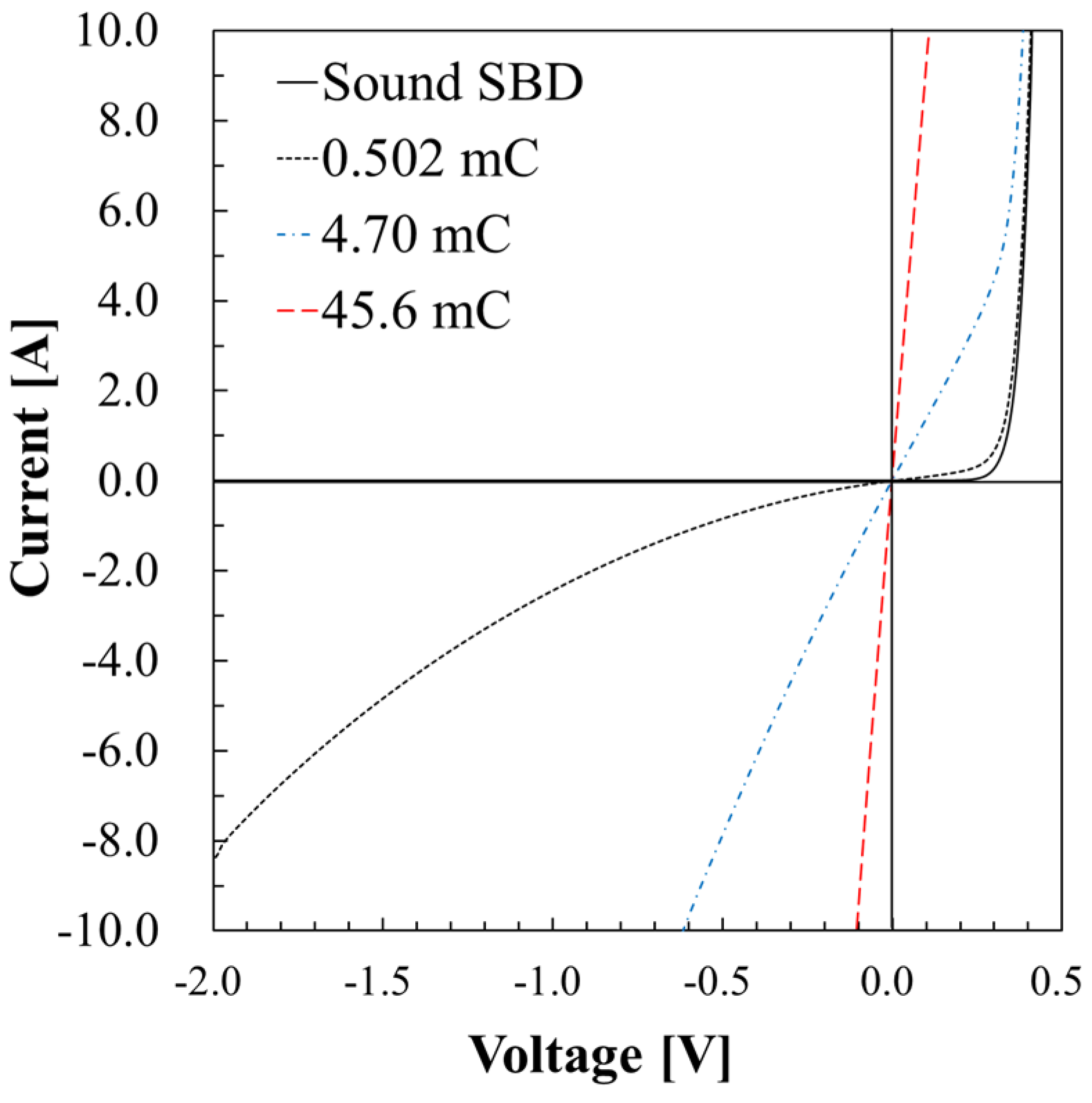
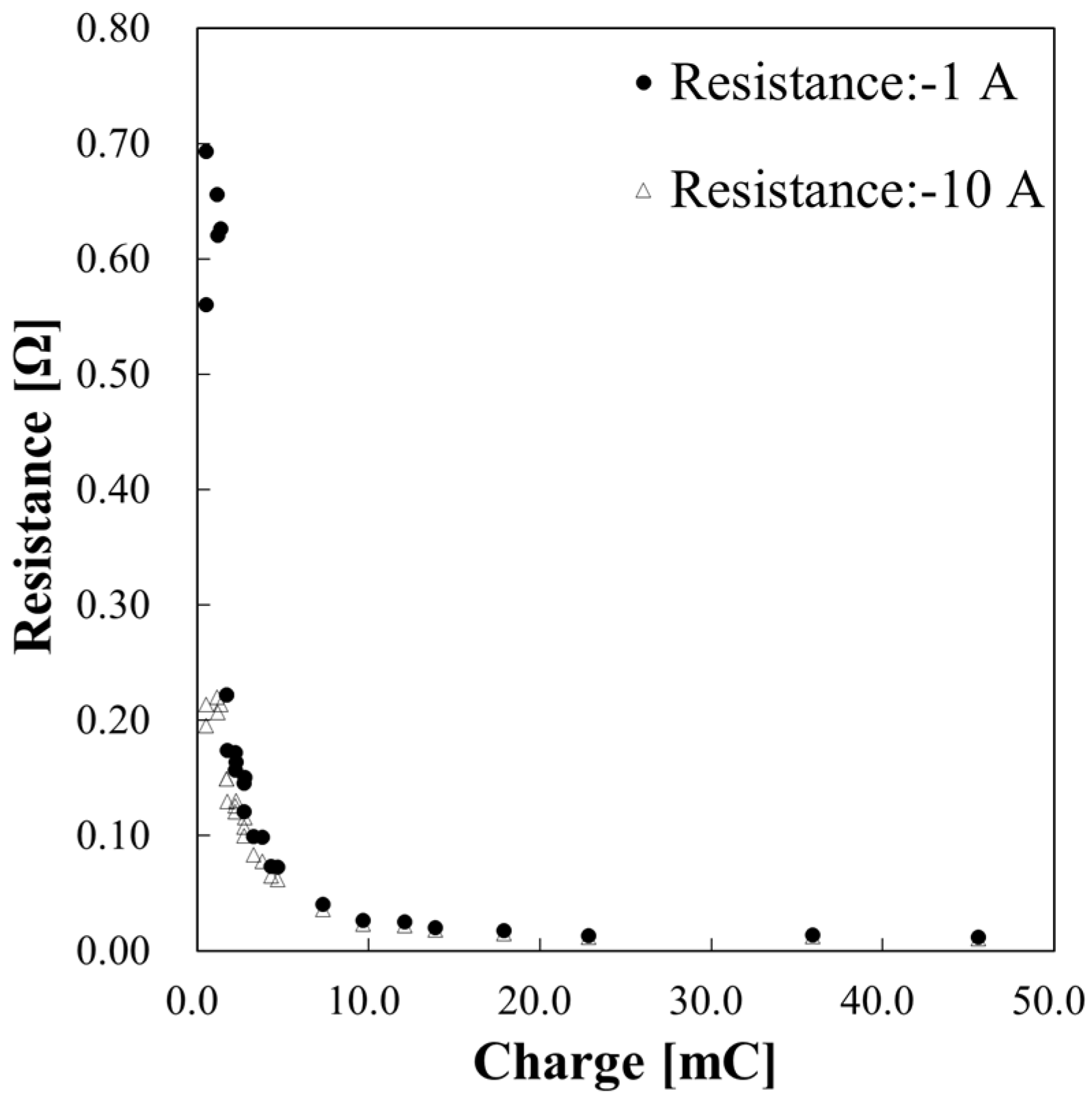
The Schottky barrier diodes that failed due to the indirect lightning surge short-circuited in both the indirect lightning surge forward and reverse stress tests. In addition, the failure resistance of the Schottky barrier diodes decreased when the electric charge of the indirect lightning surge increased.
(2)
The bypass diodes that failed during indirect lightning surges with relatively low electric charge were likely to fail at resistance values of approximately 10−1 Ω to 10 Ω and were at a high risk of heat generation and burnout.
(3)
The Schottky barrier diodes failing with indirect lightning surge forward stress were observed to fail across a wider range of indirect lightning surge electric charges compared with those failing with reverse stress. The failure resistance values reaching those at high risk of heat generation were from 10−1 Ω to 10 Ω.
(4)
For the failed Schottky barrier diodes, we confirmed the melting and loss of the Schottky barrier contact comprising the solder material and metal within an element with a semiconductor, owing to the heat generated by the indirect lightning surge current. Consequently, the melted Schottky barrier junction region in a failed Schottky barrier diode was in a low-resistance-value short-circuit condition. However, in the sound region, the diode exhibited residual electrical characteristics.
These results confirmed that a bypass diode will short-circuit during an indirect lightning surge, and the failure resistance will change depending on the charge of the indirect lightning surge. In addition, bypass diode short circuits may cause heat generation and burnout from the circulating current formed by the cell string, as well as short-circuited bypass diode and reverse current from the sound module string. These incidents can be effectively prevented by installing a fuse to cut off the overcurrent in each module string and selecting bypass diode materials with a higher forward current and reverse withstand voltage than the existing Schottky barrier diodes, such as PN junction diodes and silicon carbide devices.

Author Contributions

Conceptualization, T.H.; methodology, T.H., I.N., M.F., N.I. and S.O.; validation, T.H.; resources, T.H.; data curation, T.H.; writing—original draft preparation, T.H.; writing—review and editing, T.H., I.N., M.F., N.I. and S.O.; supervision, T.H.; project administration, T.H.; funding acquisition, T.H. All authors have read and agreed to the published version of the manuscript.

Funding

This work was supported by JSPS KAKENHI (Grant No. JP21H01580) and New Energy.

Data Availability Statement

Data will be made available on request.

Acknowledgments

The authors would like to thank K. Nakamoto, T. Miyahara, and A. Nakao for their technical assistance with the experiments.

Conflicts of Interest

The authors declare no conflict of interest.

References

  1. Takeya, K. Photovoltaic System Case Study Guide; Lightning Protection and Design Method; Design Technology Series; Kagakujyoho shuppan Co., Ltd.: Tsukuba, Japan, 2015; pp. 94–99. [Google Scholar]
  2. Koentges, M.; Kurtz, S.; Packard, C.; Jahn, U.; Berger, K.A.; Kato, K.; Friesen, T.; Liu, H.; Van Iseghem, M. Review of Failures of Photovoltaic Modules; Photovoltaic Power Systems Program; Report IEA-PVPS T13-01; IEA: Paris, France, 2014. [Google Scholar]
  3. Jiao, T.; Chen, W.; Li, Z.; Diao, Z.; Dang, X.; Chen, P.; Dong, X.; Zhang, Y.; Zhang, B. Fabrication of Ga2O3 Schottky Barrier Diode and Heterojunction Diode by MOCVD. Materials 2022, 15, 8280. [Google Scholar] [CrossRef]
  4. Haeberlin, H. Interference Voltages induced by Magnetic Fields of Simulated Lihgtning Currents in Photovoltaic Modules and Arrays. In Proceedings of the 17th EU-PVSEC, Munich, Germany, 22–26 October 2001; pp. 2343–2346. [Google Scholar]
  5. Haeberlin, H. Damages at Bypass Diodes by Induced Voltages and Currents in PV Modules Caused by Nearby Lightning Currents. In Proceedings of the 22nd EU-PVSEC, Milano, Italy, 3–7 September 2007. [Google Scholar]
  6. Haeberlin, H.; Kaempfer, M. Measurement of Damages at Bypass Diodes by Inuced Voltages and Currents in PV Modules Caused by Nearby Lightning Currents with Standard Waveform. In Proceedings of the 23rd EU-PVSEC, Valencia, Spain, 1–5 September 2008. [Google Scholar]
  7. Xiao, C.; Hacke, P.; Johnston, S.; Sulas-Kern, D.B.; Jiang, C.S.; Al-Jassim, M. Failure analysis of field-failed bypass diodes. Prog. Photovolt. 2020, 28, 909–918. [Google Scholar] [CrossRef]
  8. Lee, C.G.; Shin, W.G.; Lim, J.R.; Kang, G.H.; Ju, Y.C.; Hwang, H.M.; Chang, H.S.; Ko, S.W. Analysis of electrical and thermal characteristics of PV array under mismatching conditions caused by partial shading and short circuit failure of bypass diodes. Energy 2021, 218, 119480. [Google Scholar] [CrossRef]
  9. Hamada, T.; Azuma, T.; Nanno, I.; Ishikura, N.; Fujii, M.; Oke, S. Impact of Bypass Diode Fault Resistance Values on Burnout in Bypass Diode Failures in Simulated Photovoltaic Modules with Various Output Parameters. Energies 2023, 16, 5879. [Google Scholar] [CrossRef]
  10. Ishikura, N.; Okamoto, T.; Nanno, I.; Hamada, T.; Oke, S.; Fujii, M. Simulation Analysis of Really Occurred Accident Caused by Short Circuit Failure of Blocking Diode and Bypass Circuit in the Photovoltaics System. In Proceedings of the International Conference on Renewable Energy Research and Applications (ICRERA2018), Paris, France, 14–17 October 2018. [Google Scholar]
  11. JEC-0202:1994; Impulse Voltage and Current Tests in General. Japanese Industrial Standards Committee: Tokyo, Japan, 1994.
  12. Nakamoto, K. Large Current Impulse Test for the Metal Flame of a Photovoltaic Solar Module. J. Inst. Electr. Install. Eng. Jpn. 2020, 40, 10–11. (In Japanese) [Google Scholar]
  13. IEC 61000-4-5:2014; Electromagnetic Compatibility (EMC)—Part 4–5: Testing and Measurement Techniques—Surge Immunity Test. Japanese Industrial Standards Committee: Tokyo, Japan, 2011.
Figure 1. Schematic of the indirect lightning surge test system.
Energies 16 07792 g001
Figure 2. Combination waveform of an indirect lightning surge. (a) Open-circuit voltage waveform; (b) short-circuit current waveform.
Energies 16 07792 g002
Figure 3. Current–voltage (IV) characteristics of Schottky barrier diodes (SBDs) to which an indirect lightning surge is applied (in the reverse stress).
Energies 16 07792 g003
Figure 4. Resistance characteristics of a failed Schottky barrier diode (SBD) to which an indirect lightning surge is applied (in the reverse stress).
Energies 16 07792 g004
Figure 5. Current–voltage (IV) characteristics of a Schottky barrier diode (SBD) to which an indirect lightning surge is applied (in the forward stress).
Energies 16 07792 g005
Figure 6. Resistance characteristics of failure of a Schottky barrier diode (SBD) to which an indirect lightning surge is applied (in the forward stress).
Energies 16 07792 g006
Figure 7. Waveforms of applied voltage and current of a Schottky barrier diode (SBD) in an indirect lightning surge test. (a) Reverse stress at VSET = 0.1 kV; (b) reverse stress at VSET = 0.3 kV; (c) forward stress at VSET = 2.5 kV; (d) forward stress at VSET = 2.9 kV.
Energies 16 07792 g007aEnergies 16 07792 g007b
Figure 8. Optical and SEM images of the sound Schottky barrier diode (SBD). (a) Optical image of the outer packaging of the opened SBD; (b) cross-sectional SEM of the sound SBD; (c) SBD left end in (b); (d) SBD right end in (b).
Energies 16 07792 g008
Figure 9. Optical and SEM images of short-failure Schottky barrier diode (SBD) during an indirect lightning surge (Qs = 0.934 mC, reverse stress). (a) Optical image of the outer packaging of the opened SBD; (b) cross-sectional SEM of the sound SBD; (c) SBD left end in (b); (d) SBD right end in (b).
Energies 16 07792 g009
Figure 10. Optical and SEM images of short-failure Schottky barrier diode (SBD) during an indirect lightning surge (Qs = 29.5 mC, forward stress). (a) Optical image of the outer packaging of the opened SBD; (b) cross-sectional SEM of the sound SBD; (c) SBD left end in (b); (d) SBD right end in (b).
Energies 16 07792 g010
Disclaimer/Publisher’s Note: The statements, opinions and data contained in all publications are solely those of the individual author(s) and contributor(s) and not of MDPI and/or the editor(s). MDPI and/or the editor(s) disclaim responsibility for any injury to people or property resulting from any ideas, methods, instructions or products referred to in the content.

