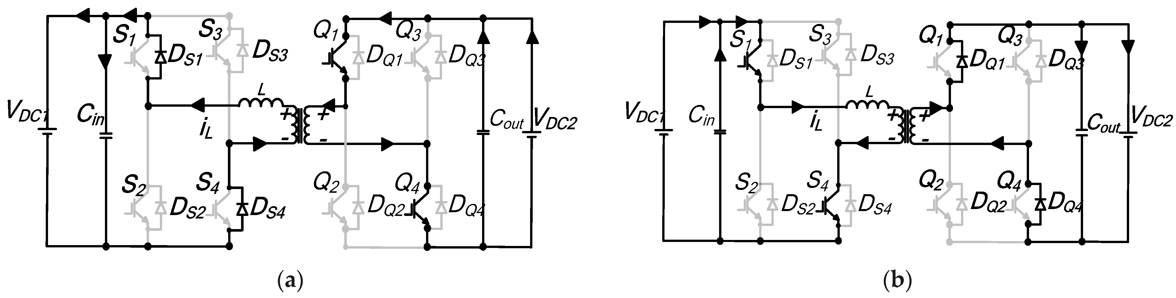
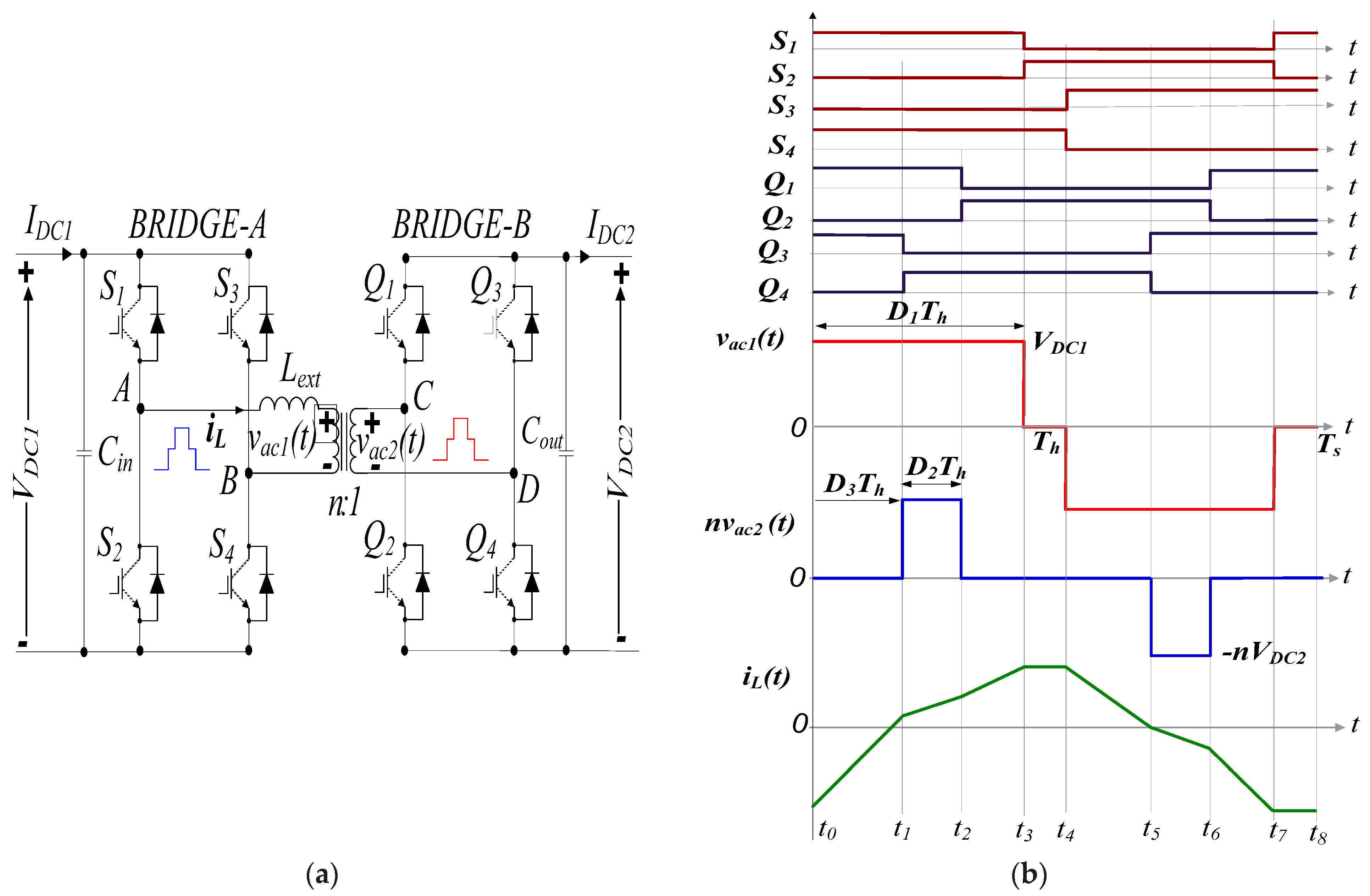
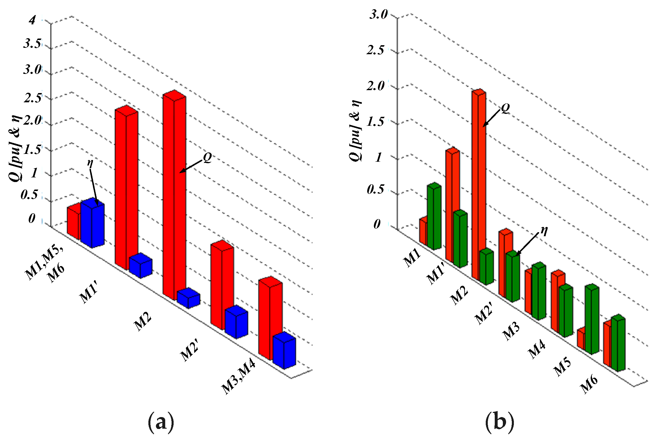
Remaining TPS Modes of Operation 2 to 6, including Its Complements
- (a)
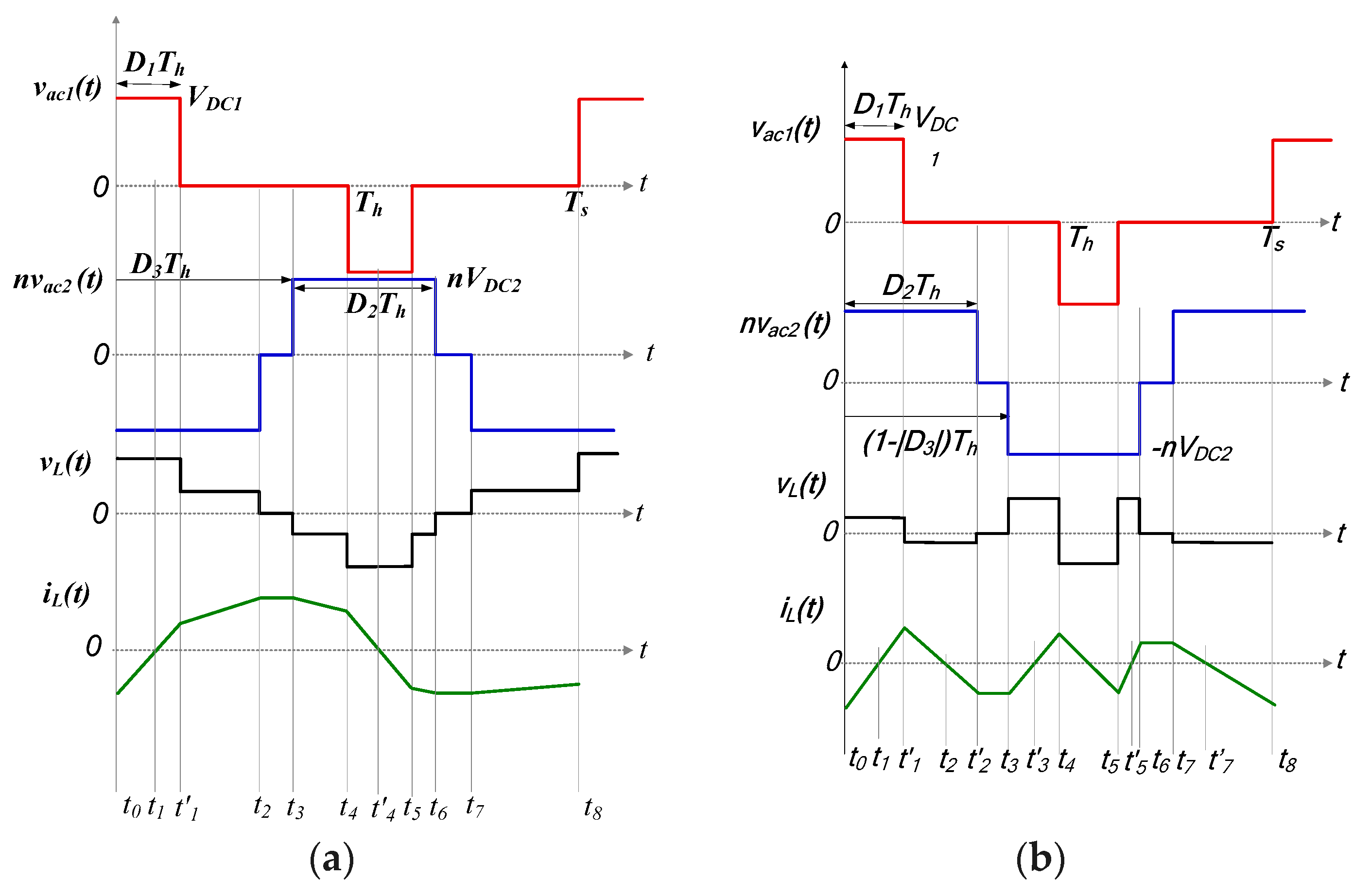
Modes 2 and 2′
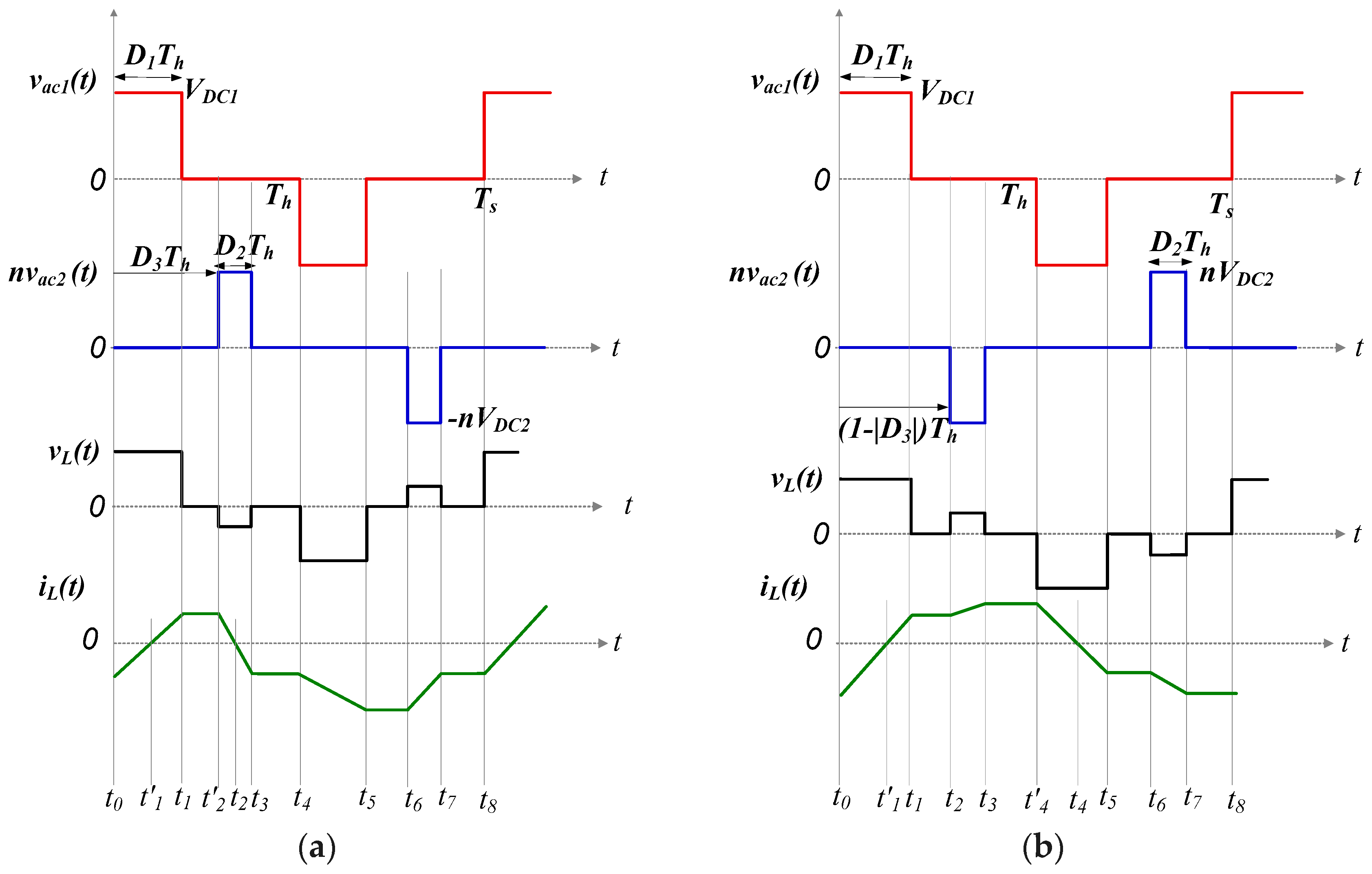
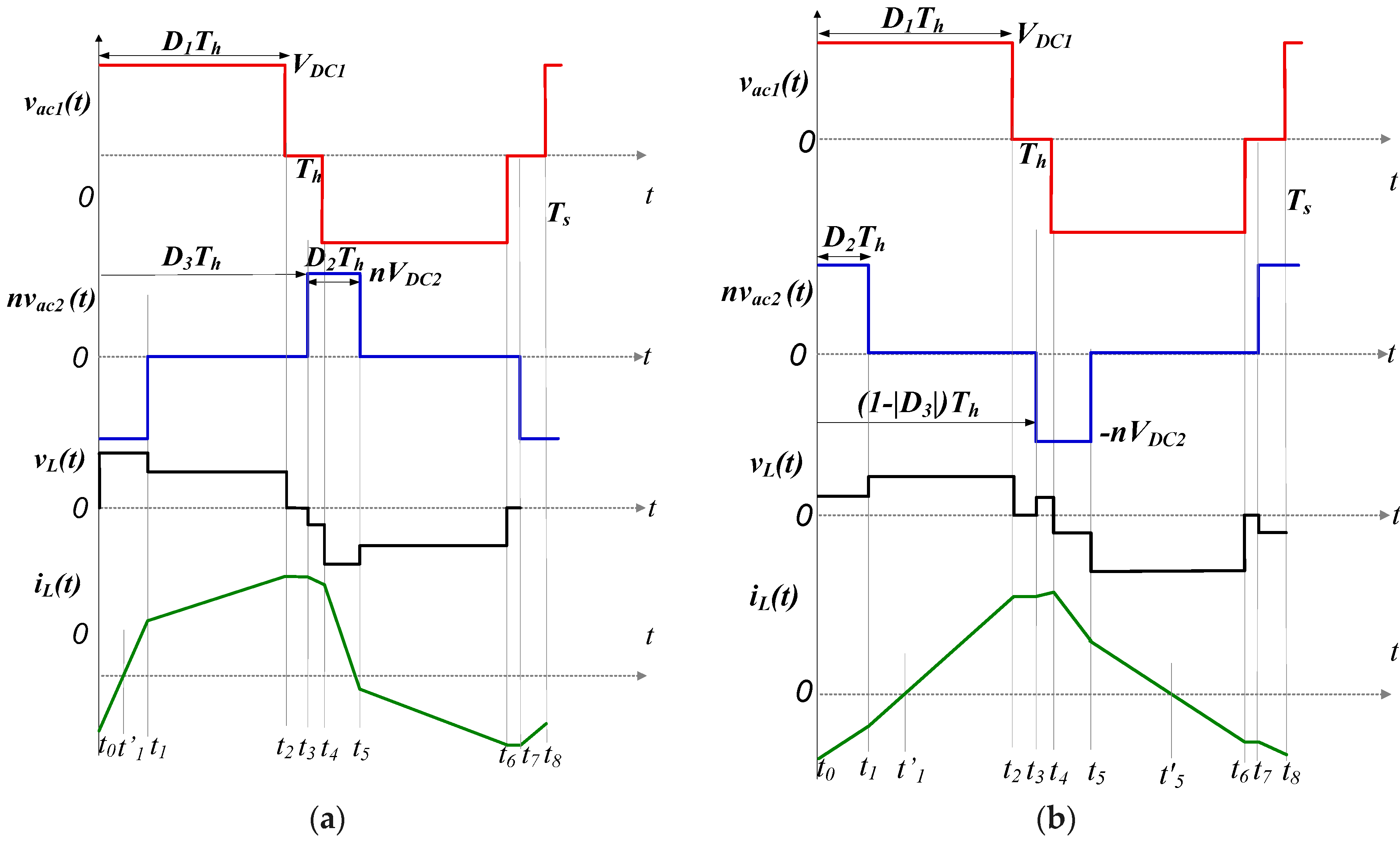
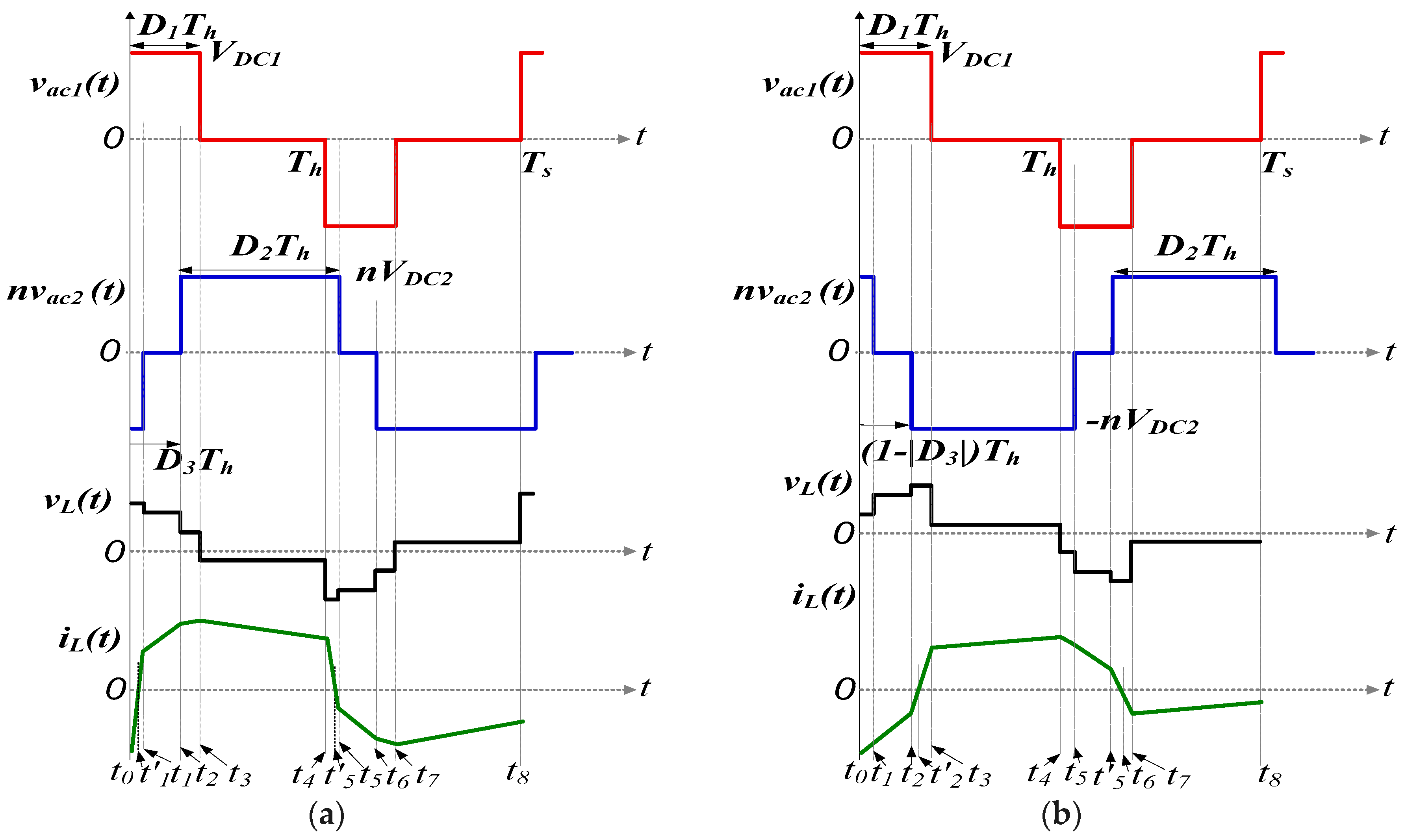
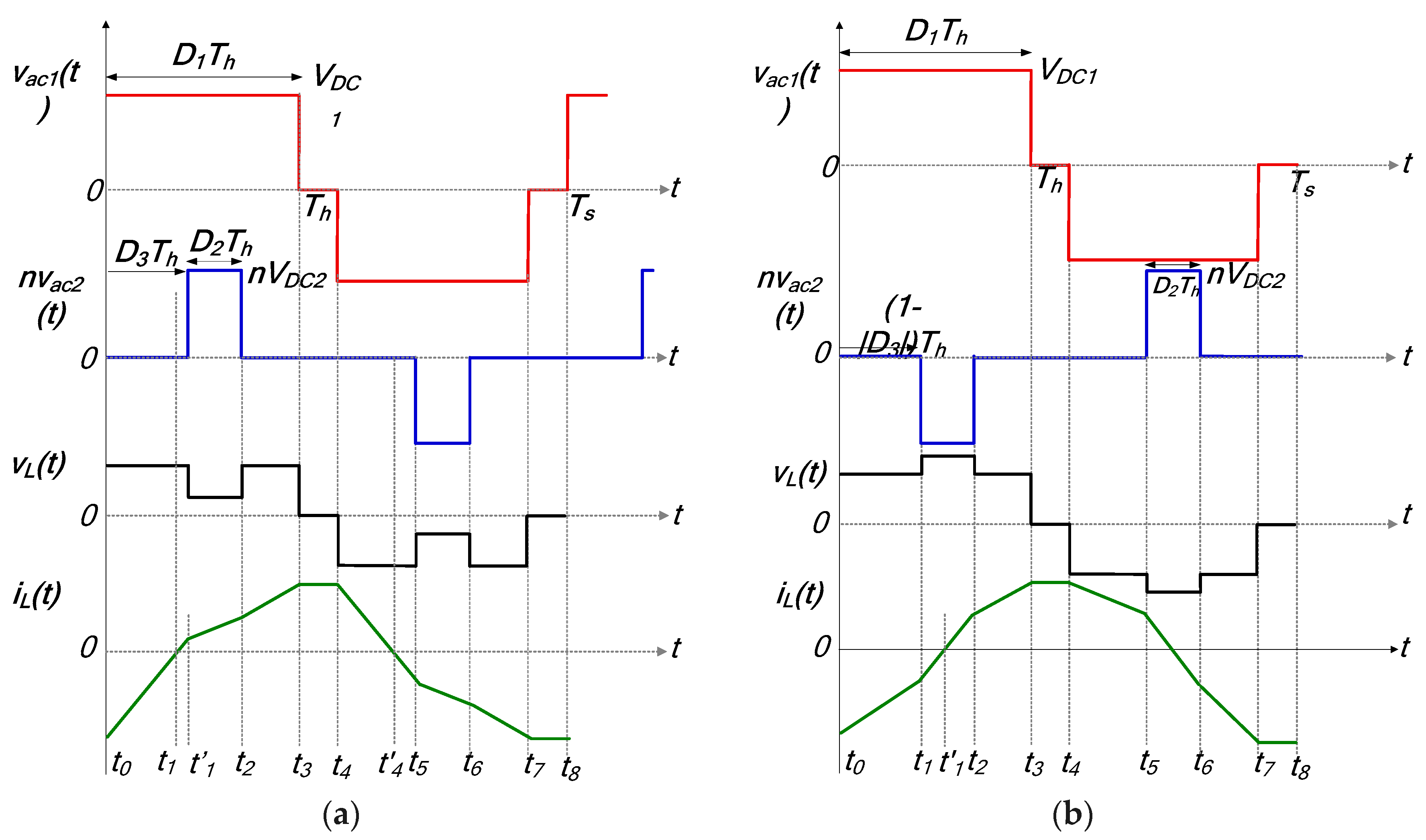
The voltage/current waveforms for these modes of operation are depicted in
Figure A1. In mode 2, operational waveforms portrayed in
Figure A1a are characterized by the full overlap of positive and negative transformer voltages. Similarly, for mode 2′, the full overlap
vac1 and
vac2 of both voltage waveform features distinguishes the mode, as
Figure A1b demonstrates. In addition, the inductor current (
iL) at each instantaneous current interval and average input/output current are also indicated.
Figure A1.
Ideal steady-state transformer voltages/inductor currents: (a) mode 2; (b) mode 2′.
Figure A1.
Ideal steady-state transformer voltages/inductor currents: (a) mode 2; (b) mode 2′.
- i.
Mode 2
The mode boundary is determined by ensuring the full overlap of positive
vac1 and negative
vac2 transformer voltages. Through observation of voltage waveform features of
Figure A1a, the following constraint is defined for the mode.
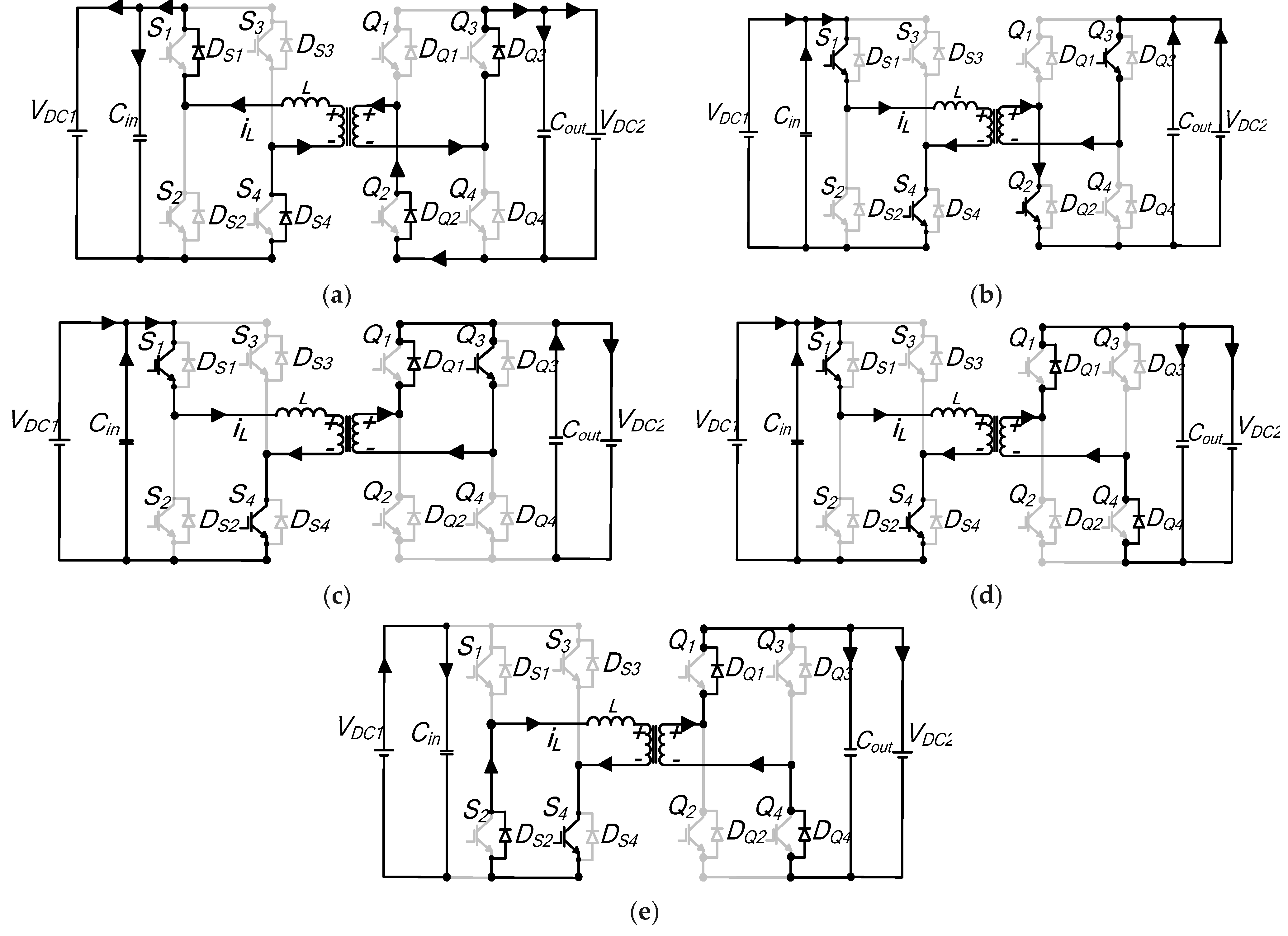
Analysis of various switching instants of the inductor current during the first half switching cycle is explained below.
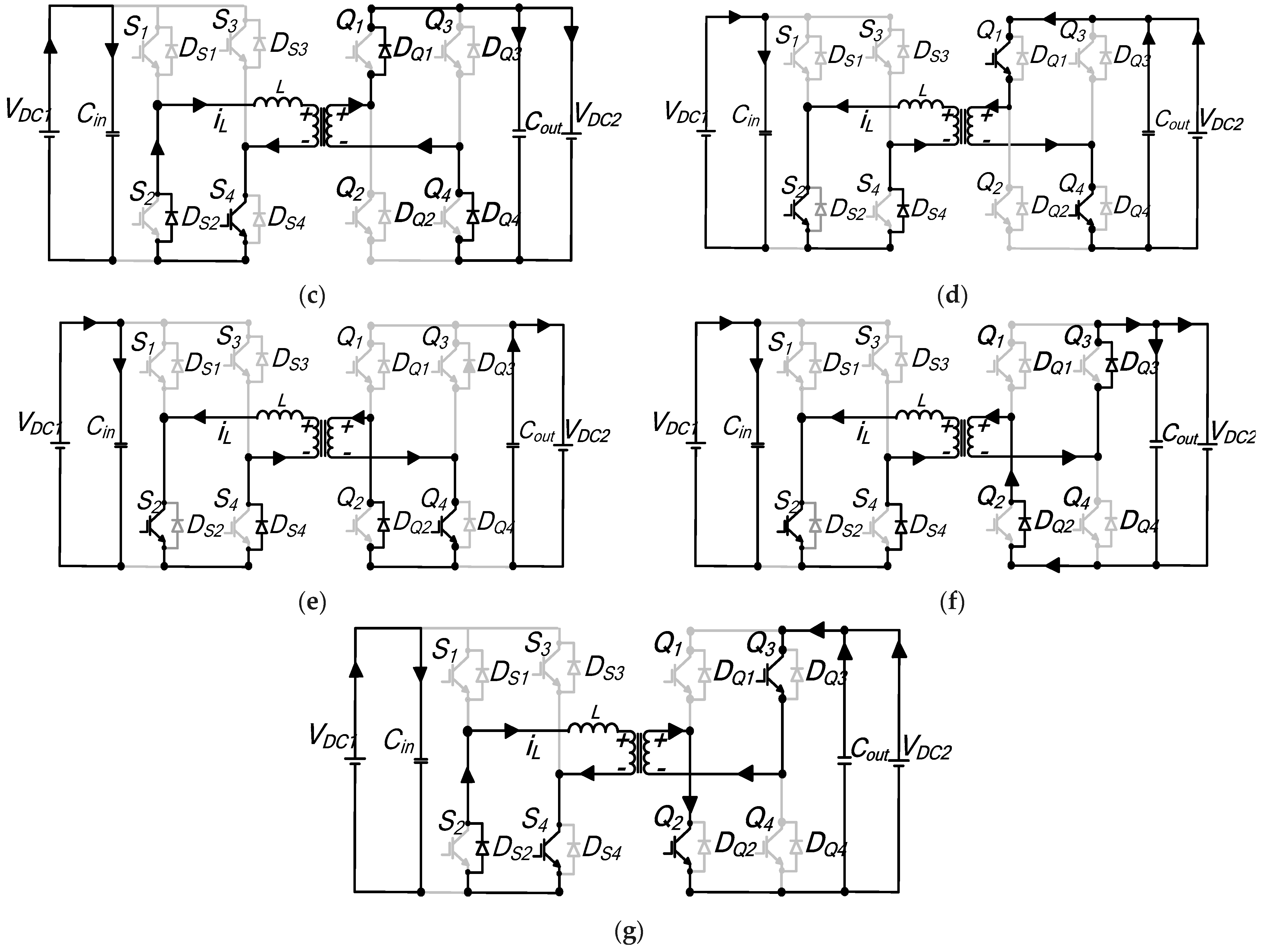
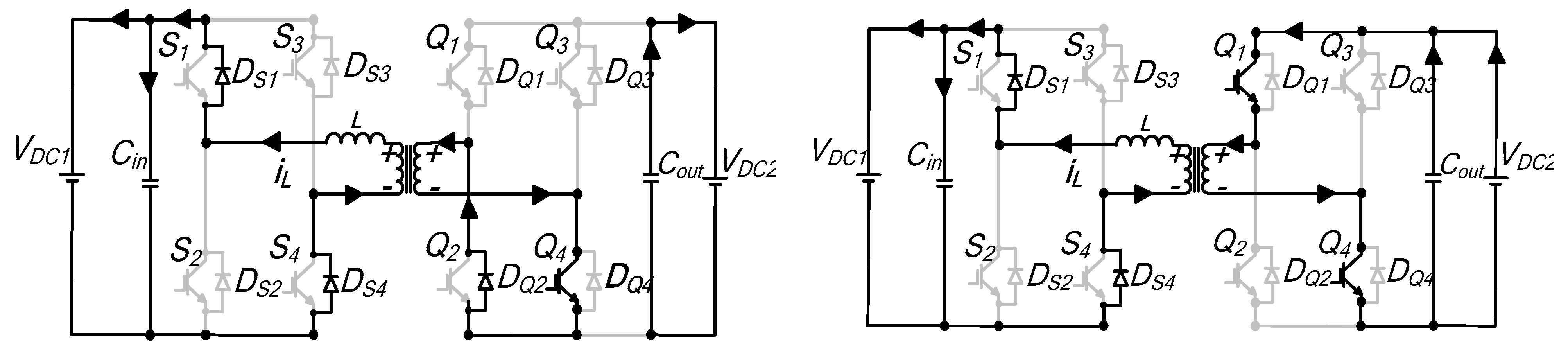
Interval t0–t1: During this sequence, the initial inductor current is negative; hence, the current flows through reverse recovery diodes
DS1 and
DS4 for bridge A, while in bridge B, antiparallel diodes
DQ2 and
DQ3 carry the current.
Figure A2a shows the resulting equivalent circuit. The inductor voltage can be expressed as
VDC1 +
nVDC2. Therefore,
iL is
Interval t1–t1′: The current polarity reverses during this segment and the equivalent circuit of
Figure A2b demonstrates the new current path. In bridge A, switches
S1 and
S4 start to conduct, whilst in bridge B, the current flows through switches
Q2 and
Q3, respectively. The instantaneous inductor current for this subperiod remains unchanged. Thereby, the inductor voltage also remains coupled at the
VDC1 +
nVDC2 value.
Interval t1′–t2: The current continues to increase steadily and flows in the direction shown by the equivalent circuit diagram of
Figure A2c. It flows through
DS2 and
S4 of primary bridge A, while for bridge B,
Q2 and
Q3 are still conducting. The voltage impressed across the inductor is
nVDC2, and thus, the inductor current is determined by
Interval t2–t3: The time sequence begins upon the switch
Q2 turn-off. Both AC transformer voltages are zero, and hence, the voltage across the inductor equates to zero. The current continues to freewheel in
DS2 and through
S4, in bridge A, while in bridge B,
DQ1 and
Q3 conduct the current, as portrayed in
Figure A2d. The current is retained at the same level as in the previous interval.
Interval t3–t4: Figure A2e shows the schematic diagram demonstrating the current path during this subperiod that completes one half-cycle. In bridge A, the current continues in a similar path as in the previous interval for bridge A. For bridge B, the current flows through
DQ1 and
DQ4. The voltage across the inductor is −
nVDC2. The inductor current is expressed as
According to
Figure A1a,
tn values are determined by assuming
t0 = 0, then
t1 =
D1Th,
t2 = (
D2 +
D3 − 1)
Th,
t3 =
D3Th and
t4 =
Th. By therefore inserting
tn values in expressions (A2) to (A4), respectively, the inductor current at various switching intervals facilitates the derivation of key performance indicators for mode 2, which are computed and listed in
Table A1. According to derivations in
Table A1, the peak current is achieved by
iL(t3). The result obtained for the mode per-unit power range is ±0.5
pu, which is similar to the previous two modes, and the TPS modulation parameters that result in these limits are given. Finally, modes can operate the converter switching devices under soft switching if the ZVS limits outlined at the bottom of
Table A1 are adhered to.
Figure A2.
Mode 2 detailed equivalent circuit diagrams: (a) to–t1; (b) t1–t′1; (c) t′1–t2; (d) t2–t3; (e) t3–t4.
Figure A2.
Mode 2 detailed equivalent circuit diagrams: (a) to–t1; (b) t1–t′1; (c) t′1–t2; (d) t2–t3; (e) t3–t4.
- ii.
Mode 2′
To visualize complimentary mode 2′ boundaries, it is paramount that the overlap of negative
vac1 and positive
vac2 transformer voltages are maintained throughout, as
Figure A1b demonstrates. Following a similar procedure as in complimentary mode 1′ and by extending the waveforms of
Figure A1b to the negative half-plane, the following mode boundary is derived:
Evaluation of the steady-state inductor current for the first half-switching cycle is performed as follows.
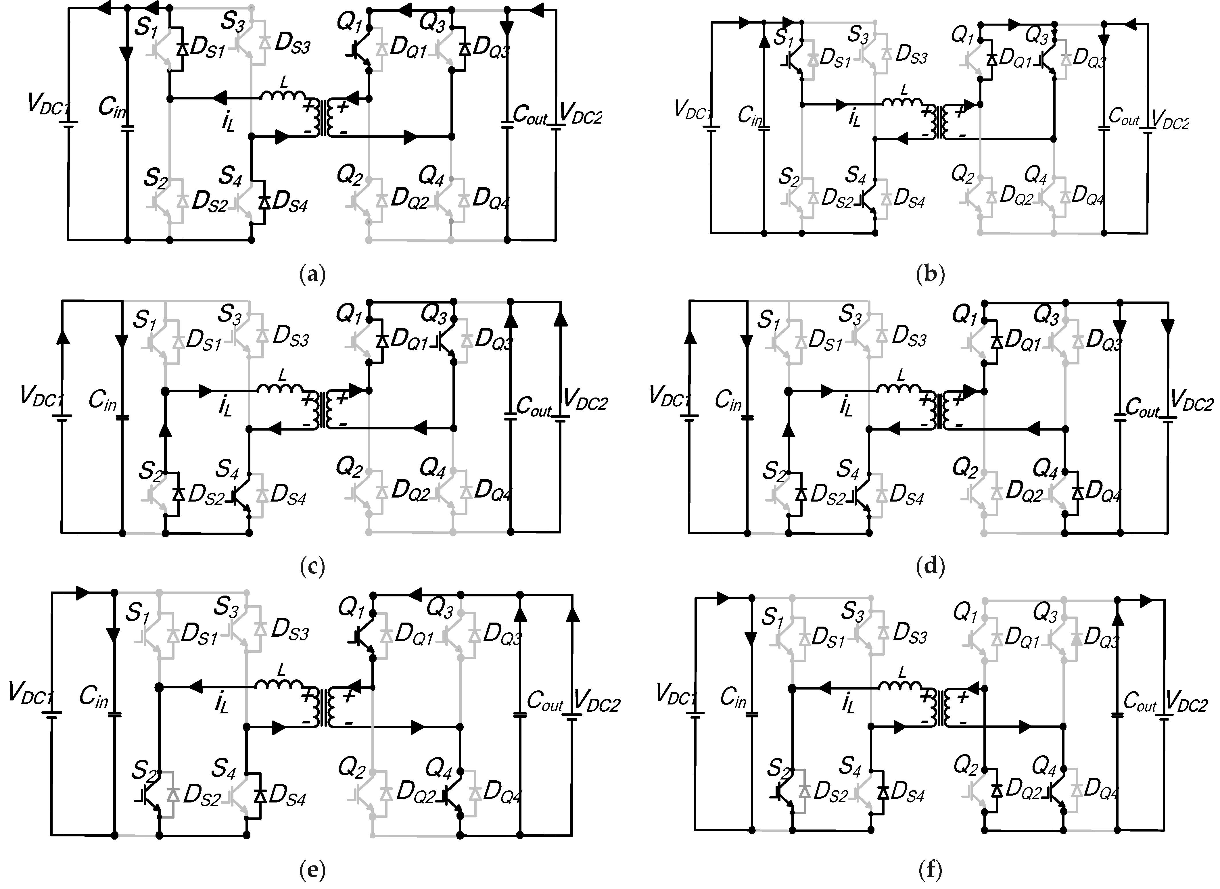
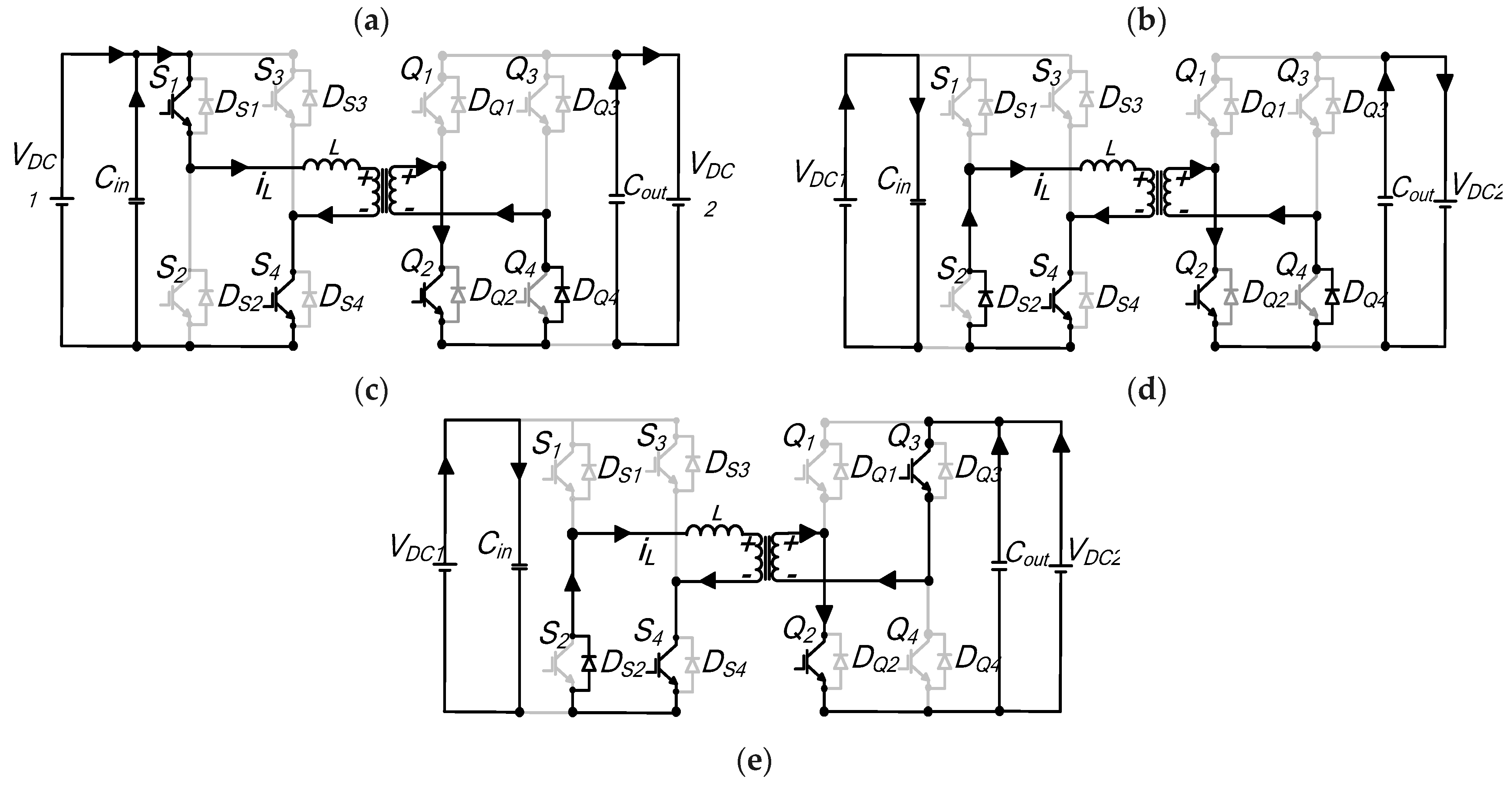
Interval t0–t1: This switching duration is illustrated by the equivalent circuit diagram of
Figure A3a. At
t0, the inductor current is freewheeling through diode
DS1 and
DS4 in H-bridge A. Switches
Q1 and
Q4 of H-bridge B conduct. The voltage impressed across
Ltot is
VDC1–nVDC2. Current
iL, which continues to increment, is given by
Table A1.
Mode 2 derivations.
Table A1.
Mode 2 derivations.
| Variable | |
|---|
| Currents at each switching instants | |
|
|
|
|
| RMS current | |
| RMS voltage | |
| Average power and range |
Range:⮕ |
| Reactive power | |
| ZVS | Achievable for all switches
Constraints: |
Interval t1–t1′: The current during this segment changes polarity, and the path it flows through is depicted in
Figure A3b. As can be seen, for bridge A, switches
S1 and
S4 are turned on, whilst reverse recovery diodes
DQ1 and
DQ4, of bridge-B carry the current. The inductor voltage is clamped at
VDC1 +
nVDC2 and the instantaneous current transferred at this segment remains unchanged.
Interval t1′–t2: Figure A3c shows the equivalent circuit for this subperiod. In bridge A, the current flows through
DS2 and
S4, while for bridge B, the antiparallel diodes
DQ1 and
DQ4 conduct. The inductor voltage during this duration is
−nVDC2, and the current can be expressed as
Figure A3.
Equivalent schematic diagram of mode 2′: (a) to–t1; (b) t1–t′1; (c) t′1–t2; (d) t2–t′2; (e) t′2–t3; (f) t′3–t3; (g) t3–t4.
Figure A3.
Equivalent schematic diagram of mode 2′: (a) to–t1; (b) t1–t′1; (c) t′1–t2; (d) t2–t′2; (e) t′2–t3; (f) t′3–t3; (g) t3–t4.
Interval t2–t′2: During this time instant shown by
Figure A3d, the inductor changes from positive to negative; it is
DS2 and
S4 of primary bridge A and
DQ1 and
Q3 of bridge B that conduct the current, respectively. The voltage impressed across the inductor remains at −
nVDC2 and thus, the current is
Interval t′2–t3: The current is the same as in expression (A8), with zero gradients, as shown by
Figure A1b. The equivalent circuit diagram of
Figure A3e shows that
DS2 and
S4 continue to conduct the current for bridge A, and it is the freewheeling diode
DQ2 and power switch
Q4 that the current flows through for H-bridge B. The inductor voltage is zero during this time sequence.
Interval t3–t′3: The inductor current increases linearly, and the voltage across the inductor is
nVDC2. For bridge A,
S2 and
DS4 conduct, while in bridge B, the current freewheels in
DQ2 and
DQ3, as depicted in
Figure A3f. The inductor voltage is
nVDC2, which causes the current to increment gradually.
Interval t′3–t4: At
t′3, the current changes polarity.
DS2 and
S4 are conducting in bridge A, while
Q2 and
Q3 are turned on. Current magnitude and inductor voltage are retained at same value as in the previous switching instant. This is displayed in
Figure A3.
Therefore, from Equations (A6)–(A9), the instantaneous inductor current at each switching interval can be determined by assuming
t0 = 0,
t1 =
D1Th,
t2 =
(D2 −
|D3|)Th,
t3 = (1
|D3|)
Th,
t4 =
Th. These expressions are listed in
Table A2, together with the derivation of other important mode parameters. The maximum current is given by |
iL(t4)| and the resulting power range for this complimentary mode is also evaluated to be ±0.5
pu Moreover, ZVS is achievable for all switches, and the boundaries for soft switching are given by the inequalities tabulated.
Table A2.
Mode 2′ steady-state expressions.
Table A2.
Mode 2′ steady-state expressions.
| Variable | |
|---|
| Currents at each switching instant | |
|
|
|
|
| RMS current | |
| RMS voltage | |
| Average power and range |
Range:⮕ |
| Reactive power | |
| ZVS | Achievable for all switches
Constraints: |
- (b)
Modes 3 and 3’
Mode 3 converter waveforms, which are shown in
Figure A4a, are characterized by non-overlapping primary and secondary transformer voltages (
vac1 and
vac2). The corresponding voltage and inductor current waveforms for complementary mode 3′ are indicated in
Figure A4b.
Figure A4.
Modes’ steady-state voltages and currents: (a) mode 3; (b) mode 3′.
Figure A4.
Modes’ steady-state voltages and currents: (a) mode 3; (b) mode 3′.
- i.
Mode 3
By following the previous steps to determine the mode constraint, inequalities defining the mode 3 boundary from the voltage sequence of
Figure A4a are determined as
Similarly, from
Figure A4a, the piecewise linear inductor current, during different subperiods, is determined over a half-cycle as follows.
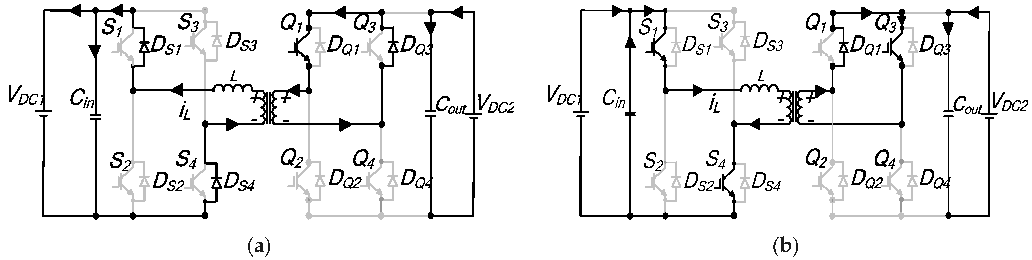
Interval t0–t′1: Figure A5a shows the equivalent circuit. The inductor current is in negative; for bridge A, the current flows through the reverse recovery diodes
DS1 and
DS4.
Q1 and
DQ3 of secondary bridge B provide a path for the current. The voltage impressed across
Ltot is
VDC1. Thus,
iL can be written as
Interval t′1–t1: At
t′1, the current changes polarity and becomes positive. Switches
S1 and
S4 of bridge A are turned on, while
DQ1 and
Q3 of the secondary bridge B are in the conduction path, as shown in
Figure A5b. The inductor voltage during this interval is retained at
VDC1 and the magnitude of the inductor current remains unchanged, which is given by expression (A11).
Interval t1–t′2: During this segment, both
vac1 and
vac2 AC voltages are zero. The
iL remains at the same value according to the previous segment, while flowing through
DS2,
S4,
DQ1 and
Q3 of both H-bridges, respectively, as
Figure A5c demonstrates.
Interval t′2–t2: Figure A5d shows the resulting circuit structure during this sequence. The antiparallel diode
DS2 and switch
S4 continue to conduct. For bridge B,
DQ1 and
DQ4 begin to freewheel. The voltage impressed across the inductor is
−nVDC2. Therefore, the current through
Ltot is
Figure A5.
Mode 3 equivalent circuits for first half-cycle: (a) to–t′1; (b) t′1–t1; (c) t1–t′2; (d) t′2–t2; (e) t2–t3; (f) t3–t4.
Figure A5.
Mode 3 equivalent circuits for first half-cycle: (a) to–t′1; (b) t′1–t1; (c) t1–t′2; (d) t′2–t2; (e) t2–t3; (f) t3–t4.
Interval t2–t3: At
t2,
iL, polarity change from positive to negative occurs.
S2 and
DS4 start to conduct, and in bridge B, the current flows through switches
Q1 and
Q3, as shown by
Figure A5e. The inductor voltage is clamped at
−nVDC2, with the current remaining unchanged for the duration.
Interval t3–t4: Figure A5f shows the equivalent circuit for this sequence.
S2 and
DS4 of Bridge A continue to conduct, and
DQ2 and
Q4 in H bridge-B begin to conduct. Since the difference between AC voltages
vac1 and
vac2 is zero, this causes the voltage across the inductor to be zero. The inductor current remains unchanged.
Therefore, according to the analysis above and by assuming
t0 = 0,
t1 =
D1Th,
t2 =
D3Th,
t3 =
(D2 +
D3)Th and
t4 =
Th, the inductor current for the first half-cycle is computed and listed in
Table A1. The mode’s equations that comprise average current, RMS current, active power, reactive power and ZVS possibility are outlined by performing step-by-step analysis. The result of this derivation is also tabulated in
Table A1. The peak current is given by
iL(t1) for this mode. By observing the active power expression, active power transfer is independent of
D3, indicating that it can be exclusively regulated by managing the voltages across the bridge. The power range for this mode is evaluated to be a maximum of 0.5
pu and a minimum of 0
pu. This shows that the mode is only capable of unidirectional power transfer. ZVS for all switches is not possible, but rather, the mode partially achieves soft switching for some of the switches.
Table A3.
Mode 3 mathematical expressions.
Table A3.
Mode 3 mathematical expressions.
| Variable | |
|---|
| Currents at each switching instant | |
|
|
|
|
| RMS current | |
| RMS voltage | |
| Average power and range |
Range:⮕ |
| Reactive power | |
| ZVS | Not achievable for all switches
Constraints: none |
- ii.
Mode 3′
According to the operating waveforms of
Figure A4b, the following two constraints are evaluated for mode 3′.
Steady-state analysis for the first half-switching cycle of the mode 3′ current waveform of
Figure A4b is explained below.
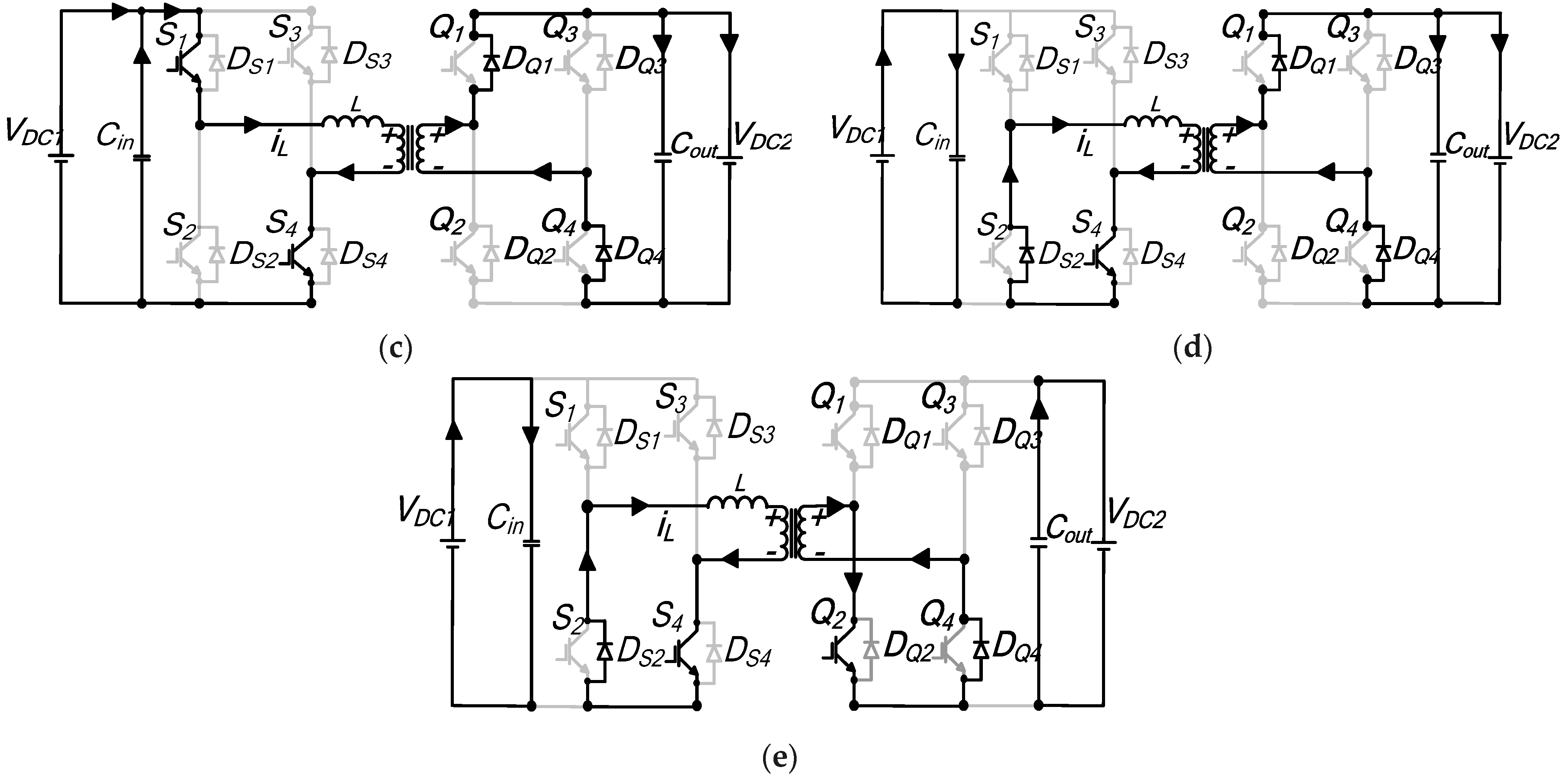
Interval t0–t′1: The inductor current starts from a negative value;
DS1 and
DS4 are both conducting for Bridge A. For bridge B, it is
DQ2 and switch
Q4 that carry the current. The equivalent circuit for this subperiod is shown in
Figure A6a. The inductor voltage is
VDC1 and current is equivalent to
Figure A6.
Mode 3′ equivalent circuit diagrams: (a) to–t′1; (b) t′1–t1; (c) t1–t2; (d) t2–t3; (e) t3–t′4.
Figure A6.
Mode 3′ equivalent circuit diagrams: (a) to–t′1; (b) t′1–t1; (c) t1–t2; (d) t2–t3; (e) t3–t′4.
Interval t′1–t1: Figure A4b depicts the current path during this instant. At
t′1, a polarity reversal of the current occurs. It is switches
S1 and
S4 of bridge A that carry the current, whilst the current flows through
Q2 and
DQ4 in the second bridge. The inductor voltage continues to be clamped at
VDC1, and the
iL magnitude remains unchanged.
Interval t1–t2: The slope of the current is zero, due to zero inductor voltage. For bridge A, the current circulates between
DS2 and
S4, as
Figure A6c shows. For the second H-bridge, the current flows through switches
DQ1 and
DQ4. The inductor current remains unchanged for the entire segment.
Interval t2–t3: The current gradually ramps up during this sequence.
Figure A6d shows the resulting equivalent circuit highlighting the current path. It is
DS2 and
S4 of bridge A that are still conducting, and for the second H-bridge, the current flows through switches
Q2 and
Q3. The interval ends when
Q2 is turned off. The voltage across the coupling inductor is
nVDC2, and the current is
Interval t3–t′4: An equivalent schematic circuit is illustrated in
Figure A6e for this time instant. Since both transformer terminal voltages for this subperiod also equate to zero, the current will remain the same as segment
t2–t3 with zero slope. The current flows through
S2 and
DS4 of bridge A, while
DQ1 and
Q3 of bridge B provide a path for the current to flow through.
By substituting
tn values of
t0 = 0,
t1 =
D1Th,
t2 = (1 −
|D3|)
Th,
t3 = (1 −
|D3| +
D2)
Th and
t4 =
Th, in expressions (A13) and (A15), the inductor current at each switching interval can be evaluated.
Table A2 provides the result of the derivation. The peak current for this mode is given by
iL(t4). By following the similar step-by-step procedure of mode 1, mode steady-state equations for the average current, RMS current, and active and reactive power are derived and listed in
Table A4.
Also observe that the derived active power expression for mode 3′ similarly shows D3 independence. Mode upper and lower power range capabilities are 0 pu and −0.5 pu, respectively, providing only unidirectional transfer. ZVS for mode 3′ is unachievable for the entire range for all the switches at the same time.
- (c)
Modes 4 and 4′
Mode 4 waveforms, which are graphically depicted in
Figure A7a, can be described by the partial overlap of positive
vac1 and negative
vac2 during the first half-cycle and during the second half-cycle, and partial overlap of positive
vac2 and negative
vac1 occurs. Similarly, complimentary mode 4′ is characterized by the partial overlap of positive/negative
vac1 and
vac2 voltage waveforms for the first and second half-cycles, as
Figure A7b illustrates.
- i.
Mode 4
Considering the waveform features of
Figure A7a, mode 4 boundaries can be described as
The half-cycle inductor currents of
Figure A4a’s segments are analysed and explained below.
Interval t0–t′1: Schematic diagram of
Figure A8a shows the current path during this instant.
DS1,
DS4,
DQ2 and
DQ3 of the DAB converter are conducting. The coupling inductor voltage is clamped at
VDC1 +
nVDC2. Therefore,
iL is
Figure A7.
(a) Mode 4; (b) mode 4′, ideal steady-state waveforms.
Figure A7.
(a) Mode 4; (b) mode 4′, ideal steady-state waveforms.
Table A4.
Derived analytical expressions of mode 3′.
Table A4.
Derived analytical expressions of mode 3′.
| Variable | |
|---|
| Currents at each switching instant | |
|
|
|
|
| RMS current | |
| RMS voltage | |
| Average power and range |
Range:⮕ |
| Reactive power | |
| ZVS | Not achievable for all switches
Constraints: none |
Interval t′1–t1: At
t′1, inductor current polarity reversal occurs. Switches
S1 and
S4 of bridge A and switches
Q2 and
Q3 of bridge B are turned on. The inductor voltage is continuously clamped on at
VDC1 +
nVDC2, with no increment in the inductor current value. This is illustrated by the schematic of
Figure A8b.
Interval t1–t2: During this interval, shown in
Figure A8c, the inductor current continues to increase with bridge A’s status, remaining similar to the previous subperiod. But for bridge B,
Q2 is switched off and the current flows through
DQ1 and
Q3, respectively. The voltage across the coupling inductor is
VDC1 +
nVDC2.
Figure A8.
First half-cycle equivalent circuit diagrams of Mode 4: (a) t0–t′1; (b) t′1–t1; (c) t1–t2; (d) t2–t3; (e) t3–t4.
Figure A8.
First half-cycle equivalent circuit diagrams of Mode 4: (a) t0–t′1; (b) t′1–t1; (c) t1–t2; (d) t2–t3; (e) t3–t4.
Interval t2–t3: The equivalent circuit diagram is illustrated by
Figure A8d, whereby the current path in bridge B remains unchanged, while in bridge A, it circulates in
DS2 and
S4. The inductor current is retained at the same magnitude as in the previous time sequence.
Interval t3–t4: Figure A8e shows the resulting equivalent circuit of this segment. For bridge A,
DS2 and
S4 are still conducting, but for bridge B, the reverse recovery diodes,
DQ1 and
DQ4, provide a path for the current to flow through. The voltage impressed across
Ltot is −
nVDC2. During this instant, the current is
Currents at each switching interval for mode 4 can be deduced from expressions (A16) and (A18), by substituting
tn values of
t0 = 0,
t1 =
(D2+ D3 − 1
)Th,
t2 =
D1Th,
t3 =
D3Th and
t4 =
Th. These are given in
Table A5. The magnitude of
iL(t2) results in mode peak current. The corresponding expressions for steady-state RMS current, average current, and active and reactive power equations are indicated in
Table A5. However, it can be seen that the maximum and minimum power limits are evaluated as 0.67
pu and 0
pu, respectively. This only represents positive unidirectional power transfer capability. Finally, soft switching is realizable for all switches under this mode of operation and the corresponding constraints are also listed in
Table A5.
Table A5.
Mathematical expressions for mode 4.
Table A5.
Mathematical expressions for mode 4.
| Variable | |
|---|
| Currents at each switching instant | |
|
|
|
|
| RMS current | |
| RMS voltage | |
| Average power and range |
Range:⮕ |
| Reactive power | |
| ZVS | Achievable for all switches
Constraints: |
- ii.
Mode 4′
Similarly, the mode 4′ constraint has to ensure partial overlap of positive/negative
vac1 and
vac2 voltage waveforms for the first and second half-switching cycles. Thus, from
Figure A7b, the mode 4′ boundary is given by
The current expression of each segment for the first half cycle of
Figure A7b is analyzed below.
Interval t0–t1: Figure A9a shows the equivalent circuit diagram. The current flow path for bridge A is through
DS1 and
DS4, while for bridge B, switches
Q1 and
Q4 conduct. The voltage imposed on the inductor is
VDC1–nVDC2. The segment ends when
Q1 is turned off. Thus,
iL(t) is written as
Interval t1–t′1: The current continues to be negative and circulates between
DS1 and
DS4 of bridge A. For bridge B,
DQ2 start to freewheel and switch
Q4 is still turned on. The voltage across
Ltot is
VDC1. The equivalent schematic showing the converter for this duration is depicted in
Figure A9b. The current for this duration is
Interval t′1–t2: During this duration that is portrayed in
Figure A9c, at
t′1, the current changes polarity, and therefore, switches
S1 and
S4 of bridge A start to conduct, while
Q2 and
DQ4 of the second bridge B carry the current. The inductor voltage is still clamped at
VDC1. The current
iL remains the same as in the previous interval. The segment ends when
S1 is turned off.
Interval t2–t3: The value of the current during this subperiod also remains unchanged, and both transformer terminal voltages are confined to a zero state, resulting in zero inductor voltage. The equivalent circuit of
Figure A9d illustrates the current path, with
DS2,
S4,
Q2 and
DQ4 playing the pivotal role of conducting for both DAB H-bridges.
Figure A9.
Mode 4′ equivalent circuit diagrams for the first half-cycle: (a) to–t1; (b) t1–t′1; (c) t′1–t2; (d) t2–t3; (e) t3–t4.
Figure A9.
Mode 4′ equivalent circuit diagrams for the first half-cycle: (a) to–t1; (b) t1–t′1; (c) t′1–t2; (d) t2–t3; (e) t3–t4.
Interval t3–t4: Figure A9e shows the equivalent schematic diagram during this switching instant. In bridge A, conducting devices remain unchanged, but for bridge B, switches
Q2 and
Q3 start to provide a path for the current path. The voltage across the coupling inductor is
nVDC2. Therefore,
iL, which is linearly increasing, is deduced as
Based on the above analysis, the inductor current at each switching segment is evaluated by assuming
t0 = 0,
t1 = (
D2–|
D3|)
Th,
t2 =
D1Th,
t3 = (1–|
D3|)
Th and
t4 =
Th. The resulting values of the current at each switching instant are shown in
Table A4. Using these current values, other vital parameters of complementary mode 4′ are similarly derived and summarized in
Table A4. The peak inductor current is given by equation
iL(t4). As can be observed also, the mode permits only unidirectional reverse power flow with the upper and lower active power limits given by 0.0
pu and −0.67
pu, respectively. The corresponding TPS modulation parameters are also listed. In addition, it is worth mentioning that ZVS for this mode is not realizable for all of the switches.
- (a)
Modes 5 and 5′
Figure A10 shows modes 5 and 5′ operating waveforms. As indicated, Mode 5 of
Figure A10a is characterized by partial overlap of positive
vac1 and positive
vac2 for the first half-cycle and vice versa during the second half-cycle. Complementary mode 5′ waveforms, which are plotted in
Figure A10b, are described by the partial overlap of positive
vac1 and negative
vac2 during the first half-cycle.
Figure A10.
Steady-state transformer voltages and inductor currents: (a) mode 5; (b) mode 5′.
Figure A10.
Steady-state transformer voltages and inductor currents: (a) mode 5; (b) mode 5′.
- i.
Mode 5
Table A6.
Derived analytical expressions representing mode 4′.
Table A6.
Derived analytical expressions representing mode 4′.
| Variable | |
|---|
| Currents at each switching instant | |
|
|
|
|
| RMS current | |
| RMS voltage | |
| Average power and range |
Range:⮕ |
| Reactive power | |
| ZVS | Not achievable for all switches
Constraints: none |
The mode half switching intervals of
Figure A10a can be divided into five segments which are analyzed as follows.
Interval t0–t′1: During this interval, the current circulates between the reverse recovery diodes
DS1 and
DS4 of bridge A, while in bridge B, it is
Q1 and
DQ3 that provide a path for the current to flow through. This is illustrated in the equivalent circuit of
Figure A11a. The voltage across the inductor is
VDC1, and therefore, the inductor’s current is expressed as
Interval t′1–t1: Figure A11b shows the equivalent diagram. As a result of current polarity reversal, switches
S1 and
S4 of H bridge A conduct, while in bridge B, the current is carried by
DQ1 and
Q3. The voltage across the inductor continues to be clamped at
VDC1, and the current during this instant remains constant.
Interval t1–t2: The time instant starts upon the turn-off of switch
Q3. The current continues to slowly increment; the bridge A switching pattern is similar to the previous segment, but for bridge B, the current starts to flow through
DQ1 and
DQ4. This is illustrated by
Figure A11c. The inductor voltage is
VDC1 −
nVDC2, and the current
iL during this duration is expressed as
Interval t2–t3: Figure A11d shows the equivalent circuit. The same current path exists for bridge B, but for H bridge A,
DS2 and
S4 provide a path for the current to pass through. The inductor voltage is given by −
nVDC2. Thus,
iL for this instant can analytically be represented as
Figure A11.
Equivalent circuits of mode 5: (a) to–t′1; (b) t′1–t1; (c) t1–t2; (d) t2–t3; (e) t3–t4.
Figure A11.
Equivalent circuits of mode 5: (a) to–t′1; (b) t′1–t1; (c) t1–t2; (d) t2–t3; (e) t3–t4.
Interval t3–t4: Transformer terminal voltages are zero during this duration. The current remains constant with a value given by expression (A26), and thus, no instantaneous power is transferred.
Figure A11e shows the equivalent circuit diagram. In bridge A,
DS2 and
S4 conduct the current, and in the second H bridge,
Q2 and
DQ4.
Table A7.
Mode 5 key performance indicators.
Table A7.
Mode 5 key performance indicators.
| Variable | |
|---|
| Currents at each switching instant | |
|
|
|
|
| RMS current | |
| RMS voltage | |
| Average power and range |
Range:⮕ |
| Reactive power | |
| ZVS | Not achievable for all switches
Constraints: none |
According to Equations (A24)–(A26), the values of the inductor current at each subperiod are evaluated by assuming
t0 = 0,
t1 =
D3Th,
t2 =
D1Th,
t3 =
(D2 +
D3)Th and
t4 =
Th. As shown in
Table A7, the final mathematical equations for the inductor current at each instant, average current, RMS current, average power and reactive power are obtained for mode 5. Based on this analysis, it can be concluded that
iL(t2) gives the peak inductor current. The mode achieves only unidirectional power flow, with corresponding upper and lower power transfer limits of 0.67
pu and 0.0
pu, respectively. Finally, soft switching for all switches is unattainable for this mode, but rather, ZVS is only partially obtainable for some of the switches.
- ii.
Mode 5′
By shifting the waveforms of
Figure A10b, to the negative half-plane, the mode 5′ constraint can be expressed as
Five segments emerge for the first half-switching cycle, based on the waveforms of
Figure A10b, which are briefly described below.
Interval t0–t′1: As shown in the circuit structure of
Figure A12a, antiparallel diodes
DS1 and
DS4 of bridge A conduct, while for the second bridge, the current flows through diode
DQ2 and switch
Q3. The inductor voltage is clamped at
VDC1 and the current continues to ramp up and is expressed as
Interval t′1–t1: Diodes
DS1 and
DS4 are still conducting for bridge A; however, for bridge B,
DQ3 and diode
DQ2 start to freewheel, as shown in
Figure A12b. The coupling inductor voltage is
VDC1 +
nVDC2. The current continues to increment, and its value is deduced as
Figure A12.
Mode 5′ detailed equivalent circuits for first half-cycle sequence: (a) to–t′1; (b) t′1–t1; (c) t1–t2; (d) t2–t3; (e) t3–t4.
Figure A12.
Mode 5′ detailed equivalent circuits for first half-cycle sequence: (a) to–t′1; (b) t′1–t1; (c) t1–t2; (d) t2–t3; (e) t3–t4.
Interval t1–t2: At
t′1, the current changes polarity, with switches
S1,
S4,
Q3 and
Q4 of both bridges providing the current path, as illustrated in
Figure A12c. The magnitude of the current remains similar to the previous segment, and the inductor voltage is clamped at
VDC1 +
nVDC2.
Interval t2–t3: Switches
Q3 and
Q4 are still conducting for bridge B, while
DS2 and
S4 of bridge A provide a path for the current to flow through, as depicted in
Figure A12d. The inductor voltage is given by
nVDC2. Therefore, the
iL slope can be written as
Interval t3–t4: The subperiod starts when
Q2 is switched off. Both transformer AC voltages are zero. The equivalent circuit is plotted in
Figure A12e. The current path for bridge A still remains unchanged, and for bridge B, the antiparallel diode
DQ1 and switch
Q3 conduct the current.
IL is unchanged for this duration.
Based on the analysis above, analytical expressions for the mode currents and other key indices are calculated by assuming
tn values of,
t0 = 0,
t1 = (1 −
|D3|)
Th,
t2 =
D1Th,
t3 = (1 −
|D3| + D2)
Th and
t4 =
Th. The resulting values of the derivations for mode 5′ are tabulated in
Table A6. The maximum current obtained is
iL(t3) =
iL(t4). The mode is capable of only unidirectional power range of 0.0
pu and −0.67
pu. Moreover, ZVS is achievable across all switches and the resulting inequalities that define the soft-switching boundary are also given in
Table A8.
- (e)
Modes 6 and 6′
Figure A13 illustrates the operational waveforms of modes 6 and 6′. Mode 6, displayed by
Figure A13a, is characterized by the partial overlap of positive
vac2 with positive and negative
vac1. The complementary mode 6′ waveforms of
Figure A13b portray inverse features of mode 6′.
Figure A13.
Ideal voltage/current waveforms of (a) mode 6; (b) mode 6′.
Figure A13.
Ideal voltage/current waveforms of (a) mode 6; (b) mode 6′.
Table A8.
Key derivations for mode 5′.
Table A8.
Key derivations for mode 5′.
| Variable | |
|---|
| Currents at each switching instant | |
|
|
|
|
| RMS current | |
| RMS voltage | |
| Average power and range |
Range:⮕ |
| Reactive power | |
| ZVS | Achievable for all switches
Constraints: |
- i.
Mode 6
Mode constraint is determined by observing the voltage waveforms of
Figure A13a and ensuring that the waveform features are not violated. This is given by
The mode half-cycle interval for each sequence of
Figure A10a is described below.
Interval t0–t′1: The inductor current is negative; hence,
DS1 and
DS4 of bridge A are freewheeling, whilst for bridge B, the current similarly flows through the antiparallel diodes
DQ2 and
DQ3, as shown in the circuit structure of
Figure A14a. At the end of the segment, the current falls to zero and the inductor voltage is clamped at
VDC1 +
nVDC2.
IL can be deduced from
Interval t′1–t1: Polarity change for
iL occurs at
t′1.
Figure A14b shows the resulting equivalent circuit showing switches
S1,
S4,
Q2 and
Q3 providing a path for the current to flow through. The current value remains unchanged during this segment and is given by expression (A32). Similarly, the voltage impressed across the coupling inductor is retained at
VDC1 +
nVDC2.
Interval t1–t2: The plot of
Figure A14c shows the schematic diagram illustrating the current path during this subperiod. The operation of bridge A remains unchanged, while
DQ1 and
Q3 of bridge B conduct. The inductor voltage is
VDC1. The current starts to ramp up and can be expressed according to
Interval t2–t3: As can be seen on
Figure A14d, during this time instant, switches
S1 and
S4 are still conducting, while for bridge B, the reverse recovery diodes
DQ1 and
DQ4 carry the current. The inductor voltage is
VDC1–nVDC2, and
iL continues to rise steeply, with a gradient determined by
Interval t3–t4: During this segment,
DQ1 and
DQ4 of H bridge B still provide a path for the current to flow through, and for H bridge A, the current starts to circulate between
DS2 and
S4. The equivalent circuit is shown in
Figure A14e. The voltage across the inductor is given as
−nVDC2 and the current slightly decreases, and is derived as
Applying similar step-by-step procedures to mode 6 and by assuming
t0 = 0,
t1 = (
D3 +
D2 − 1)
Th,
t2 =
D3Th,
t3 =
D1Th and
t4 =
Th. Solutions for mode currents, active power, reactive power and ZVS boundaries are obtained and given in
Table A9. The mode peak current is achieved by
iL(t3). It can be observed from the results of
Table A9 that the mode can operate at a maximum power of 1
pu and a minimum 0.0
pu range. Finally, soft switching is attainable for this mode, and the corresponding inequalities that define the ZVS range are listed.
- ii.
Mode 6′
Mode constraints can be determined by observing the theoretical waveforms of
Figure A10b and by shifting them to a negative half-plane. The inequalities describing the mode boundary should ensure partial overlap of positive
vac1(
t) with positive and negative of
vac2(
t), and are given by
Analyses of various switching instants of
Figure A10b waveforms for the first half-cycle interval are discussed below, and are plotted in detailed equivalent diagrams of
Figure A12.
Interval t0–t1: Figure A15a shows the current path. For bridges A and B,
DS1,
DS4,
DQ1 and
DQ4 allow the current to pass through. The voltage across the inductor is clamped at
VDC1–nVDC2, and the current through
Ltot is given by
Figure A14.
Equivalent circuit diagrams for mode 6 first half-cycle: (a) to–t′1; (b) t′1–t1; (c) t1–t2; (d) t2–t3; (e) t3–t4.
Figure A14.
Equivalent circuit diagrams for mode 6 first half-cycle: (a) to–t′1; (b) t′1–t1; (c) t1–t2; (d) t2–t3; (e) t3–t4.
Interval t1–t2: The current continues to circulate between the
DS1 and
DS4 antiparallel diodes. In bridge B, switch
Q2 and the reverse recovery diode
DQ4 allow the current to flow through, as evident in
Figure A15b. The inductor voltage is
VDC1, and thus,
iL is
Interval t2–t′2: Figure A15c demonstrates the equivalent circuit during this switching instant. The operation of bridge A remains unchanged; as the current is still negative,
DS1 and
DS4 remain in the conduction path. Meanwhile, in bridge B, the current flows through the diodes
DQ2 and
DQ3 until it decreases to zero. The voltage across the inductor is
VDC1–nVDC2, and thus,
iL is
Interval t′2–t3: At
t′2, the current changes to positive.
Figure A15d displays the current path during this subperiod. Switches
S1,
S4,
Q2 and
Q3 are turned on, respectively.
VDC1–nVDC2 is continually impressed across the inductor voltage and the
iL magnitude is unchanged.
Interval t3–t4: The current continues to ramp up gradually and the equivalent circuit structure is shown in
Figure A15e. In bridge B, the current continues to flow through switches
Q2 and
Q3, but due to the zero state of voltage
vac1,
DS2 and
S4 of bridge A conduct. The voltage across the inductor is
nVDC2, and the slope of
iL can be deduced from
Table A9.
Mode 6 expressions.
Table A9.
Mode 6 expressions.
| Variable | |
|---|
| Currents at each switching instant | |
|
|
|
|
| RMS current | |
| RMS voltage | |
| Average power and range |
Range:⮕ |
| Reactive power | |
| ZVS | Achievable for all switches
Constraints: |
According to the aforementioned analysis, the inductor current at each interval discussed above is computed by assuming
t0 = 0,
t1 =
(D2 − |D3|)
Th,
t2 = (1
− |D3|)
Th,
t3 =
D1Th and
t4 =
Th. This is provided in
Table A10 below, in addition to other modes’ important parameters being computed. Observe that the peak inductor current is obtained through
iL(t4). The derived mode active power output and range is tabulated in
Table A10, with a corresponding unidirectional upper and lower transfer limit of 0.0
pu and −1.0
pu, respectively. The converter switches can operate under ZVS with the boundary defined by the instantaneous current inequalities.
Figure A15.
Detailed equivalent circuits of mode 6′: (a) to–t1; (b) t1–t2; (c) t2–t′2; (d) t′2–t3; (e) t3–t4.
Figure A15.
Detailed equivalent circuits of mode 6′: (a) to–t1; (b) t1–t2; (c) t2–t′2; (d) t′2–t3; (e) t3–t4.
Table A10.
Mode 6′ parameters.
Table A10.
Mode 6′ parameters.
| Variable | |
|---|
| Currents at each switching instant | |
|
|
|
|
| RMS current | |
| RMS voltage | |
| Average power and range |
Range:⮕ |
| Reactive power | |
| ZVS | Achievable for all switches
Constraints: |


