Article

A Control Design Technology of Isolated Bidirectional LLC Resonant Converter for Energy Storage System in DC Microgrid Applications

Department of Electrical Engineering, National Taipei University of Technology, 1, Sec. 3, Zhongxiao E. Rd, Taipei 10608, Taiwan
*
Author to whom correspondence should be addressed.
Energies 2023, 16(19), 6877; https://doi.org/10.3390/en16196877
Submission received: 15 August 2023 / Revised: 22 September 2023 / Accepted: 25 September 2023 / Published: 29 September 2023
(This article belongs to the Special Issue Optimal Design and Application of High-Performance Power Converters)

Abstract

:
This paper presents a new control method for a bidirectional DC–DC LLC resonant topology converter. The proposed converter can be applied to power the conversion between an energy storage system and a DC bus in a DC microgrid or bidirectional power flow conversion between vehicle-to-grid (V2G) behavior and grid-to-vehicle (G2V) behavior. Furthermore, such a converter can be applied to energy storage systems for decentralized renewable energy generation systems, such as solar and wind power. In addition, this converter can be combined with a bidirectional inverter to allow energy storage in the system to improve the safety, stability, and power quality of the microgrid. In the proposed circuit structure, we use a bidirectional DC–DC LLC, which has the advantages of a higher voltage conversion ratio, lower part count, simpler control than similar converters such as DAB, CLLC, and L–LLC converters, and bidirectional power flow and electrical isolation. Specifically, to extend the battery life, it can be employed as a control strategy for discharging the energy stored in the battery (SOC) and reducing the temperature rise generated by the internal solid electrolyte interphase (SEI) when discharging the battery under the variation in distributed energy resource (DER) generation and load demand. To realize the bidirectional power conversion without using any auxiliary inductor and only changing the control strategy, the forward step-down power conversion was based on pulse frequency modulation (PFM) control, and the reverse step-up power conversion was based on pulse width modulation (PWM) control. In this paper, we introduce the bidirectional converter topology and its control strategy for the DC microgrid battery energy storage system. Finally, a 500 W prototype is built to verify the effectiveness of the proposed converter.

1. Introduction

1.1. Overview

In addition to energy supply and demand, economic efficiency, environmental protection, and impact assessment are crucial to energy development. In the face of the multiple challenges of energy security and global warming, how to ensure the security of energy supply and sustainable development of the environment are key issues that policymakers must carefully consider. Therefore, developing low-carbon energy sources and improving the efficiency of various energy uses and conversions are becoming a priority. The development of distributed generation (DG) based on renewable energy [1] and the demand for clean electricity from photovoltaic, fuel cells, wind, geothermal, and ocean energy are increasingly favored because of the low energy density of renewable energy and the high cost of traditional power generation. Most renewable energy sources are intermittent and must be stored to ensure the stability of the power supply. For example, the battery energy storage system (BESS) [2] and the electric vehicles (EVs) [3] are power storage units for different renewable energy sources and realize the vehicle-to-grid (V2G) behavior and the grid-to-vehicle behavior (G2V) [4]. Therefore, the BESS should have a bidirectional power flow capability to store energy when excess renewable energy is generated and release it when there is a shortage or during a peak in energy consumption. By incorporating storage elements into the renewable energy system, the concerns of variability and intermittency caused by integrating renewable energy with the grid can be mitigated to some extent. DC microgrids [5] can operate in one of two modes: stand-alone or grid-connected. In stand-alone mode, the local load is controlled by the renewable energy generated and the BESS. In the grid-connected mode, the power flow between DC and AC microgrids allows for more flexibility and can also provide ancillary services (A/S) [6], bringing additional benefits of decentralized grid flexibility to the generators and consumers. Figure 1 shows a typical DC microgrid structure. Since there are various renewable energy sources, such as photovoltaic panels that generate DC power, a DC–DC converter is used to connect the DC network for power conversion, and a DC–AC converter is used to transfer this renewable energy from the DC–DC converter to the AC grid, making the AC grid flexible and controllable. Accordingly, a DC–DC bidirectional converter transfers the BESS or EVs energy to the DC Bus.
Most recent research has focused on bidirectional power transfer because the bidirectional DC–DC converter is the key component in realizing the bidirectional power flow of BESS. Different topologies of bidirectional DC–DC converters have been proposed in the literature [7,8]. Bidirectional DC–DC converters can be classified into non-isolated and isolated topologies [9]. Non-isolated topologies transmit power without transformer or capacitor isolation and, therefore, lack the advantages of current isolation and high voltage gain ratio. However, they have advantages in size and weight due to their simple structure; thus, non-isolated bidirectional topologies are recommended for low-power and low-voltage gain applications. In contrast, isolated topology essentially converts the DC voltage on the primary side into a square voltage waveform and transmits it to the secondary side through a high-frequency transformer, which is then adjusted to DC output voltage. In practice, galvanic isolation is required in many specified systems for safety reasons. In addition, the voltage gain of the isolation topology can be increased by using the turn ratio of the transformer, so it is recommended for high-power and high-voltage-gain applications.

1.2. Detailed Analysis

In general, the BESS bidirectional DC–DC converter must have high power density, high efficiency, and high reliability. Various electrically isolated bidirectional DC–DC topologies have been proposed and studied in recent decades. Among these, the full-bridge phase-shift (FBPS) converter is an isolated DC–DC converter with good wide voltage regulation characteristics [10,11], but its lack of soft switching in the main circuit under light load reduces its efficiency. In addition, its topology is asymmetrical because the filter inductors are placed on the secondary side. Therefore, even if the diodes are replaced by metal-oxide-semiconductor field-effect transistors (MOSFETs) on the secondary side, it cannot efficiently achieve bidirectional power flow. In the literature [12], a control method was proposed to operate the FBPS converter in a voltage-fed mode based on phase shift modulation in the direction of forward power flow and the current-fed mode in the direction of backward power flow based on pulse width modulation. However, there was no soft switching in the current-fed mode. In addition, when the secondary switches were turned on simultaneously to magnetize the inductor, the conduction loss was increased, and the available duty cycle was reduced, potentially leading to higher voltage stress in the PSFB converter. In another study [13], various voltage input dual active bridge (DAB) converter topologies, such as phase-shift dual active bridge (PSDAB) converters, were given two bridge switches on each side of the transformer. The phase shift between the gate drive signals for the primary-side and secondary-side switches was used to determine the power flow direction and the output power. The overall efficiency was reduced because of high backward energy and high switching loss during the cutoff period. In addition, the feature of zero-voltage switching (ZVS) was inevitably lost when the converter had a wide range of voltage variations, resulting in switching losses and increased circulating currents. At light loads, the soft switching range became narrower, and the circulating current inside the DAB converter increased significantly, resulting in a rapid decrease in efficiency. Therefore, it is challenging for this converter to maintain high efficiency over a wider voltage range. Although many improved modulation strategies have been proposed, such as single-phase-shift (SPS), dual-phase-shift (DPS) [14], and triple-phase-shift (TPS) [15], their control methods are complex and switching losses are still high. The circuit topologies of the bidirectional full-bridge CLLC converter proposed in [16,17] and the bidirectional full-bridge CLLLC resonant converter proposed in [18] are derived from the LLC series resonant converter. In the bidirectional control, the primary and secondary sides have symmetrical power conversion, a full-bridge symmetrical structure of the rectifier stage, and a bidirectional power flow with the symmetrical high-frequency transformer. Therefore, from a wide voltage range point of view, LLC is not a good choice because the large voltage gain implies a smaller ratio of magnetizing inductance to resonance inductance and a wide switching frequency range, leading to design complexity and increased power loss. The CLLC–C multiple resonance converter proposed in [19] rearranges CLLC or CLLC–C resonant networks to change the quality factor of the resonant network by controlling the auxiliary switch to achieve a wider voltage range.
The LLC resonant converter is suitable for soft switching but encounters problems when used in bidirectional operation. When the converter supplies energy in the backward direction, the magnetizing inductance of the transformer is embedded in the output voltage. This phenomenon causes the magnetizing inductor to be excluded from the circuit in the resonance process. In this case, the LLC resonance can be considered an LC series resonance with a maximum voltage gain of 1. Therefore, the LLC resonant converter is not suitable for backward voltage gains and wide voltage output. The converter proposed in [20] has a symmetrical resonant circuit on the primary and secondary sides to achieve bidirectional power flow. It achieves low or high voltage gain by selecting the operation of the half-bridge or full-bridge circuit structure. Therefore, this converter can realize the output voltage with a controlled voltage increase range to avoid the wide range of switching frequency variation in conventional bidirectional resonant converters. Another study [21] proposed a full-bridge topology-based bidirectional resonant converter. In the forward operation, switching between the half-bridge and full-bridge configurations extends the output voltage range by providing a step-down gain of 0.5 or 1. In the backward operation, a double voltage rectification (DVR)-control method is used to realize a double voltage gain on the rectifier side, which can effectively extend the operating voltage range. The conventional resonant converter control method is only used for unidirectional power conversion and works only in a buck or boost mode. In the study by [22], a bidirectional synchronous/nonsynchronous rectifier control method for bidirectional LLC chargers is proposed, while a synchronous rectification was performed in the forward mode. In the backward mode, the asynchronous rectifier was performed to generate the gate drive signals with a delay angle between the secondary and primary sides, resulting in high voltage gain at low battery voltage, leading to increased power losses. In the high battery voltage range, the delay angle was adjusted to zero to achieve high efficiency. In [23], a PWM control strategy was proposed to realize the natural bidirectional power flow of LLC–DCX (DC–DC Transformer, DCX), which can operate even when the resonance parameter changes. However, since the optimal operation point is at the resonance point, deviation from the resonance point would result in circulating losses and reduced voltage gain. Several studies [24,25,26,27,28,29] proposed an L–LLC resonant structure by adding an auxiliary inductor to the conventional LLC topology so that the resonance characteristics of each resonant mode could be LLC in both directions of operation. The power loss increased by adding an auxiliary inductor across the high voltage on the secondary side.
Table 1 summarizes the above analysis and compares the existing converters. The PSFB [12] has relatively few parts and relatively poor efficiency, while DAB [15] has more parts and relatively low voltage gain with complex control. The CLLC [17] is similar to DAB [20], which has a higher number of switches and increased complexity of control in order to expand the output range and change from full-bridge to half-bridge and vice versa. The L–LLC [25] adds an auxiliary inductor across the high-voltage terminal on the secondary side to increase the power loss. It cannot achieve a wide voltage range because of its use of PFM control.

1.3. Motivation

This paper presents a design method for a bidirectional LLC resonant converter used in energy storage systems. In addition, the asymmetric characteristics of the LLC resonant converter in the forward and backward modes are studied, and the effect of asymmetry on the resonant converter is investigated. In addition, a design method for a bidirectional LLC resonant converter is presented to reduce the need for an auxiliary inductor in the design of the backward resonant circuit shown in [24,25,26,27,28,29]. Specifically, a forward buck power flow adopts a conventional LLC resonant structure by relocating the LLC resonant tank, and a backward boost power flow employs a push–pull structure with an inductor and a capacitor in the secondary-side rectifier converter (LC-SRC) resonance by relocating the LC resonant tank. Therefore, the converter combines a conventional push–pull converter with PWM control to obtain a wide input voltage range and LC–SRC resonance characteristics. This LC-SRC converter not only has all the advantages of resonance characteristics but also the following benefits:
  • The low voltage side is defined as the primary side, whereas the high voltage side is defined as the secondary side;
  • All switches have ZVS turn-on, and the body diodes of the primary-side switches have ZCS turn-off, thus reducing switching losses and improving overall efficiency;
  • Compared with the half-bridge structure, the primary side is driven by the low-side gate drivers, so no floating gate drivers are needed, thus simplifying the design of the drive circuit and reducing costs;
  • The switching duty cycle is maintained at about 0.5 to obtain the maximum component utilization;
  • The series connection of a resonant capacitor can isolate the DC current to avoid the magnetic escape of the transformer.
In the following, Section 2 introduces the basic operating principles and related theoretical derivations of the proposed forward buck LLC resonant converter topology and the backward boost LC resonant push–pull converter topology. In Section 3, the parameters of the converter are designed, and in Section 4, the digital control method of battery charging and discharging is described. Section 5 presents the experimental results of a 500 W prototype, and Section 6 concludes the discussion.

2. Topology Description

2.1. Forward Buck-Type Energy Transfer

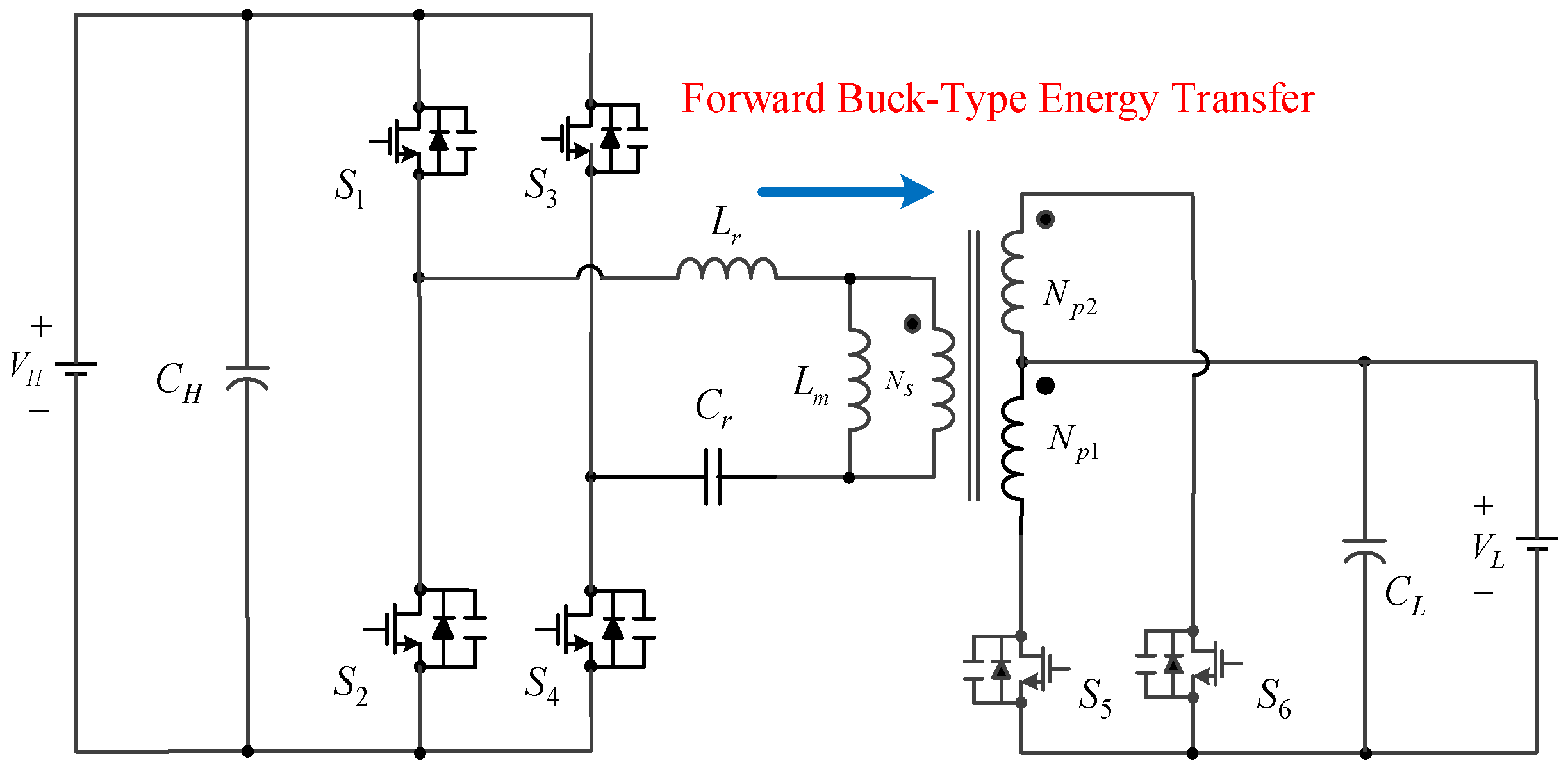
As shown in Figure 2, a typical LLC resonant converter consists of a high input voltage VH, full-bridge switches S1 to S4, an LLC resonant tank, a transformer, rectifiers S5 and S6, an output filter CL, and a load voltage VL. The resonant tank consists of a series inductor Lr, a series capacitor Cr, and a magnetizing inductor Lm. The power flows from VH through the transformer to VL.
The series inductor Lr and the series capacitor Cr form a series resonant circuit with one resonant frequency fr1 defined in Equation (1), which has the minimum impedance to a sinusoidal current with the resonant frequency fr1. The switching frequency fs for the full-bridge switches S1 to S4 is far from the resonant frequency fr1 as the high input voltage VH is increased on condition that the load voltage VL is kept constant. As the load decreases, the magnetizing inductance Lm participates in the LLC resonant operation and generates the other resonant frequency fr2, as described in Equation (2). Therefore, the switching frequency fs determined by the load conditions moves between the range of fr1 and fr2.
f r 1 = 1 2 π L r C r
f r 2 = 1 2 π ( L m + L r ) C r

2.1.1. Voltage Gain under the Turns Ratio Equal to One

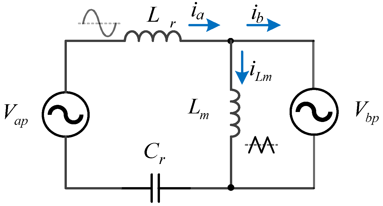
The principle of the first harmonic analysis (FHA) method is that the main component of the circulating current in the resonant circuit is a pure sinusoidal current. Therefore, by assuming that only the fundamental wave of the current transfers power to the load, ignoring all higher harmonics, the AC equivalent model of the LLC resonant converter can be obtained from the assumptions shown in Figure 3. In addition, the parasitic inductance of the output filter capacitor and the primary-side leakage inductance of the transformer are ignored, and the primary-side parameters are reflected to the secondary side.
The equivalent circuit shown in Figure 4 can be obtained by applying Thévenin’s theorem to the LLC equivalent circuit, as shown in Figure 3.
The voltage VTp is defined by Equation (3):
V T p = V a p ω s 2 C r L m ω s 2 C r ( L r + L m ) 1
The Thévenin’s equivalent impedance of the AC equivalent circuit of the LLC resonant converter can be defined as Equation (4):
Z T = j ω s L m ( ω s 2 C r L r 1 ) ω s 2 C r ( L r + L m ) 1
From (4), the Thévenin’s equivalent inductive impedance can be written as Equation (5):
L T = L m ( ω s 2 C r L r 1 ) ω s 2 C r ( L r + L m ) 1
To obtain the curves of the steady-state sinusoidal currents and voltages of the LLC converter, a phasor diagram is used to represent them, as shown in Figure 4.
The fundamental harmonic of the AC input voltage with the square wave, called VH, is given by Equation (6):
V a p = 4 V H π
The fundamental harmonic of the secondary-side AC output voltage with the square wave, called VL, which is reflected from VH, is given by Equation (7):
V b p = 4 V L π
The load current Io reflected to the secondary side, called Ibp, can be expressed by Equation (8):
I b p = π 2 I o
Figure 5 shows the synthetic phase diagram. The angle ϕ represents the phase difference between the voltages VTp and Vbp. From the analysis of the vector diagram shown in Figure 5, Equation (9) can be written.
V T p 2 = V b p 2 + ( ω s L T I b p ) 2
Substituting Equations (7) and (8) into (9) yields Equation (10):
V T p 2 = ( 4 V L π ) 2 + ( ω s L T π I o 2 ) 2
Substituting Equations (3) and (5) into (10) yields Equation (11):
( V L ) 2 = ( V H ) 2 [ ω s 2 C r L m ω s 2 C r ( L r + L m ) 1 ] 2 π 4 64 [ ω s L m ( ω s 2 C r L r 1 ) I o ω s 2 C r ( L r + L m ) 1 ] 2
where the following definitions are
M = V L V H
ω s = 2 π f s
ω r = 1 C r L r
f n = f s f r 1
λ = L r L m
I o ¯ = ω s L r V H I o
By substituting Equation (12) to (17) into (11), the voltage gain M can be expressed as Equation (18):
M = f n 4 π 4 64 [ ( f n 2 1 ) I o ¯ ] 2 f n 2 ( λ + 1 ) λ
From (18), the voltage gain is a function of the load current. The equivalent AC load resistance Rac is defined as the load resistance R reflected to the secondary side of the transformer, as shown in Equation (19). Therefore,
R a c = V b p I b p
Based on (7) and (8), rearranging (19) yields
R a c = 4 V L π 2 π I o
Equation (20) can be rewritten to
R a c = R 8 π 2
Additionally, the quality factor Q of the resonant circuit is defined as
Q = L r / C r R a c
Therefore, by substituting Equation (22) into (18) and performing appropriate algebraic operations, Equation (23) can be obtained as
M = f n 2 [ f n 2 ( λ + 1 ) λ ] 2 + [ f n Q ( f n 2 1 ) ] 2
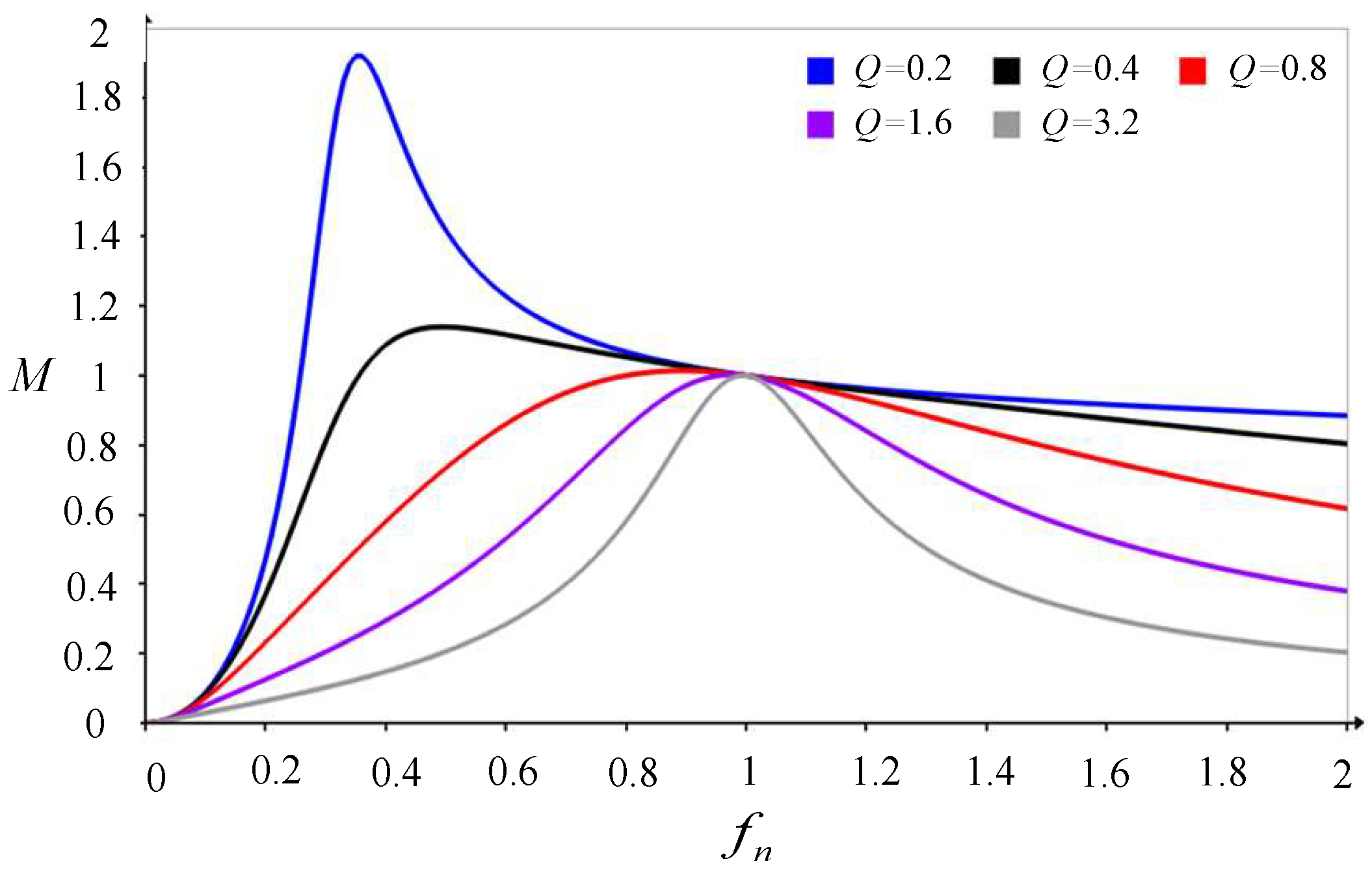
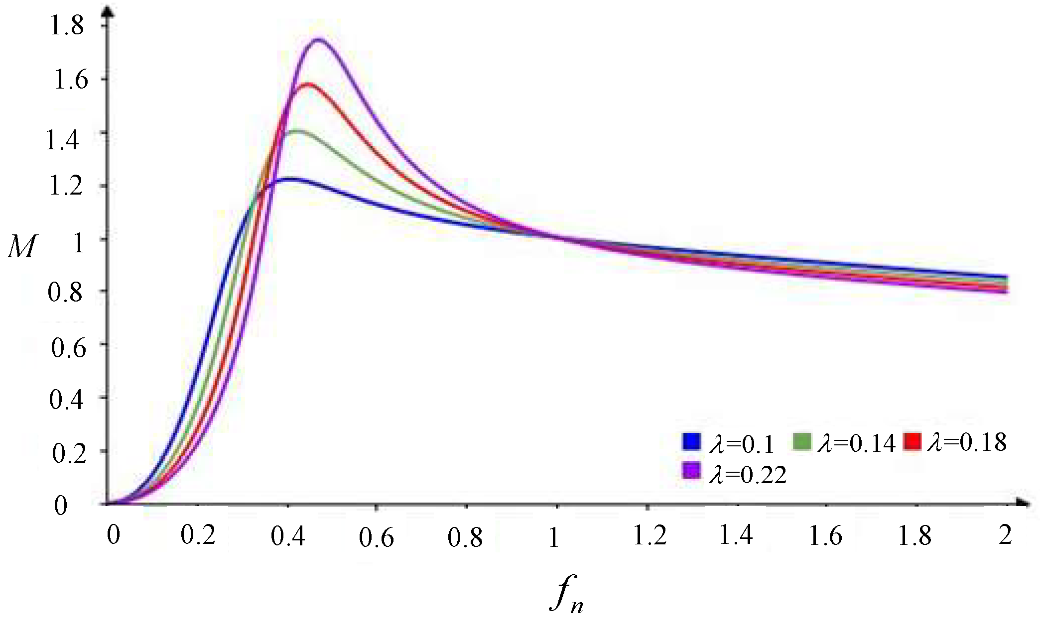
From (23), under a given value of λ, the curves of voltage gain M versus normalized switching frequency fn under different quality factors of Q are plotted in Figure 6. Using Equation (23), under a given value of Q, curves of the voltage gain M as a function of the normalized switching frequency fn from different quality factors of λ are plotted in Figure 7.

2.1.2. Operating Principles

The previous analysis considered a primary harmonic approximation equivalent circuit LLC converter where all voltages and currents are sinusoidal. In the following, the switching frequency of the LLC converter is investigated for modes where the switching frequency is lower, equal, or greater than the first resonance frequency. All the components are considered ideal, and all the primary-side parameters and loads are reflected to the secondary side. Only the waveforms within 0.5 Ts are considered, where Ts is the switching period.

Case 1: Switching Frequency Equal to Resonant Frequency (fs = fr1)

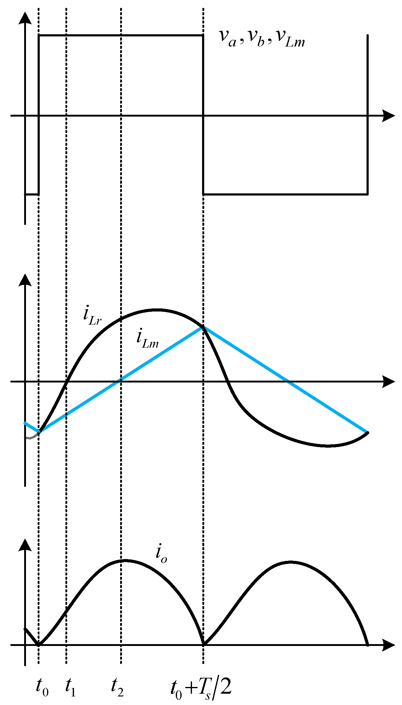
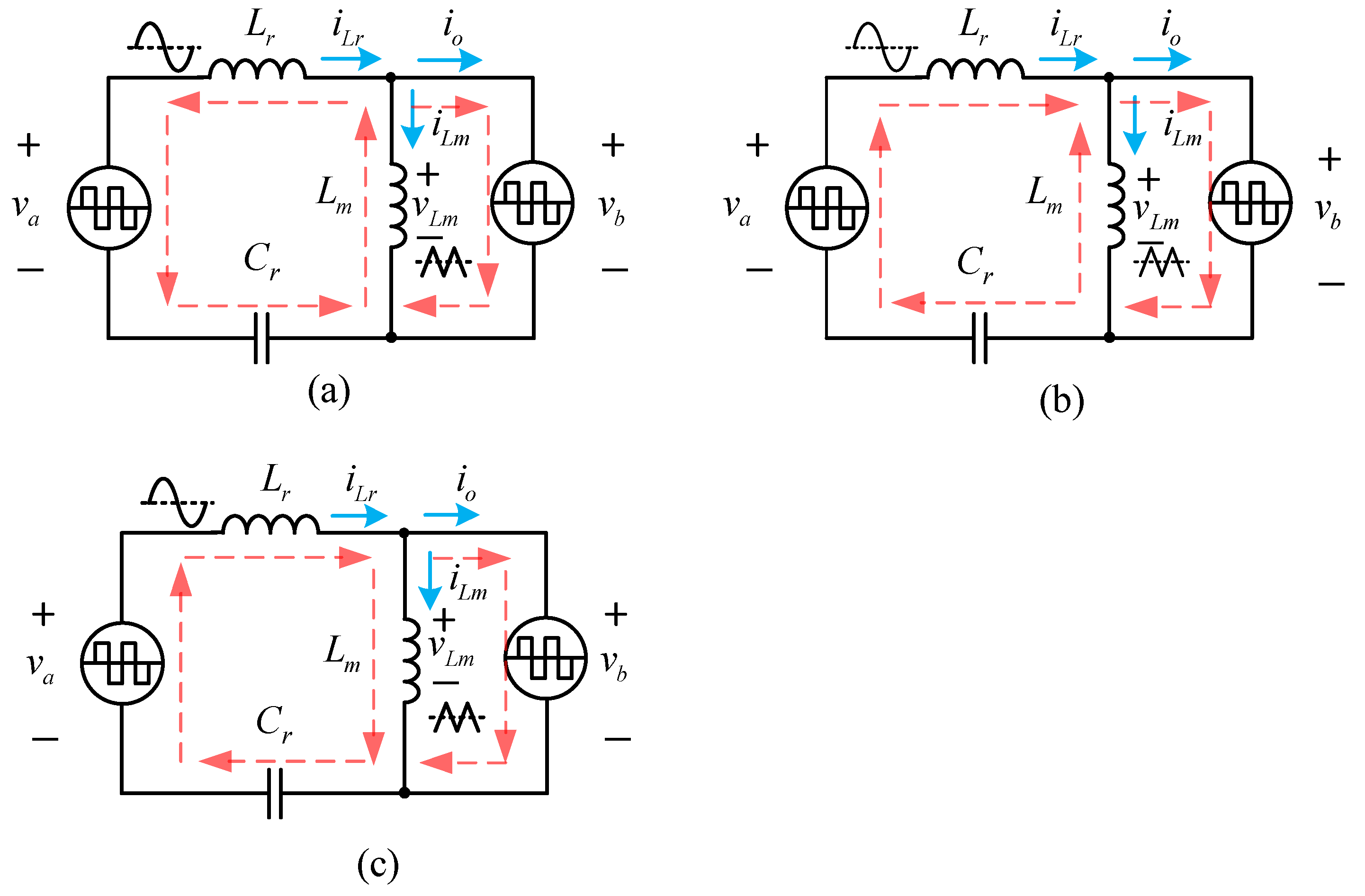
Figure 8 shows the corresponding illustrated waveforms, and Figure 9 shows the accompanying current flows in three operating modes.
Mode 1: [t0tt1]
As shown in Figure 8 and Figure 9a, since the voltages va and vLm are positive, the resonant current iLr and the magnetizing current iLm are negative with sinusoidal and linear rise, respectively. At t = t1, this mode ends at iLr = 0, proceeding to Mode 2.
Mode 2: [t1tt2]
As shown in Figure 8 and Figure 9b, the resonance current iLr is positive and increases sinusoidally, while the magnetization current iLm is negative and increases linearly. At t = t2, this mode ends at iLm = 0, proceeding to Mode 3.
Mode 3: [t2tt0 + Ts/2]
As shown in Figure 8 and Figure 9c, the resonant current iLr and the magnetizing current iLm are both positive with sinusoidal and linear rise, respectively. At t = t3, this mode ends at io = 0, proceeding to Mode 1.
At the resonant frequency, the LLC resonant converter is able to turn on the secondary-side switch with ZVS. At the same time, the turn-off current is the maximum magnetizing inductance current. By selecting a suitable magnetizing inductance, a slight turn-off loss can be achieved. In addition, the primary-side diode is turned off with low voltage across it due to di/dt, which means less reverse recovery loss. Thus, the optimal performance of the LLC resonant converter is expected at the resonant frequency. At the resonant frequency, the series resonant circuit impedance is zero. Therefore, the input and output voltages are connected, and the voltage gain at the resonant frequency is equal to one.

Case 2: Switching Frequency Greater than Resonant Frequency (fs > fr1)

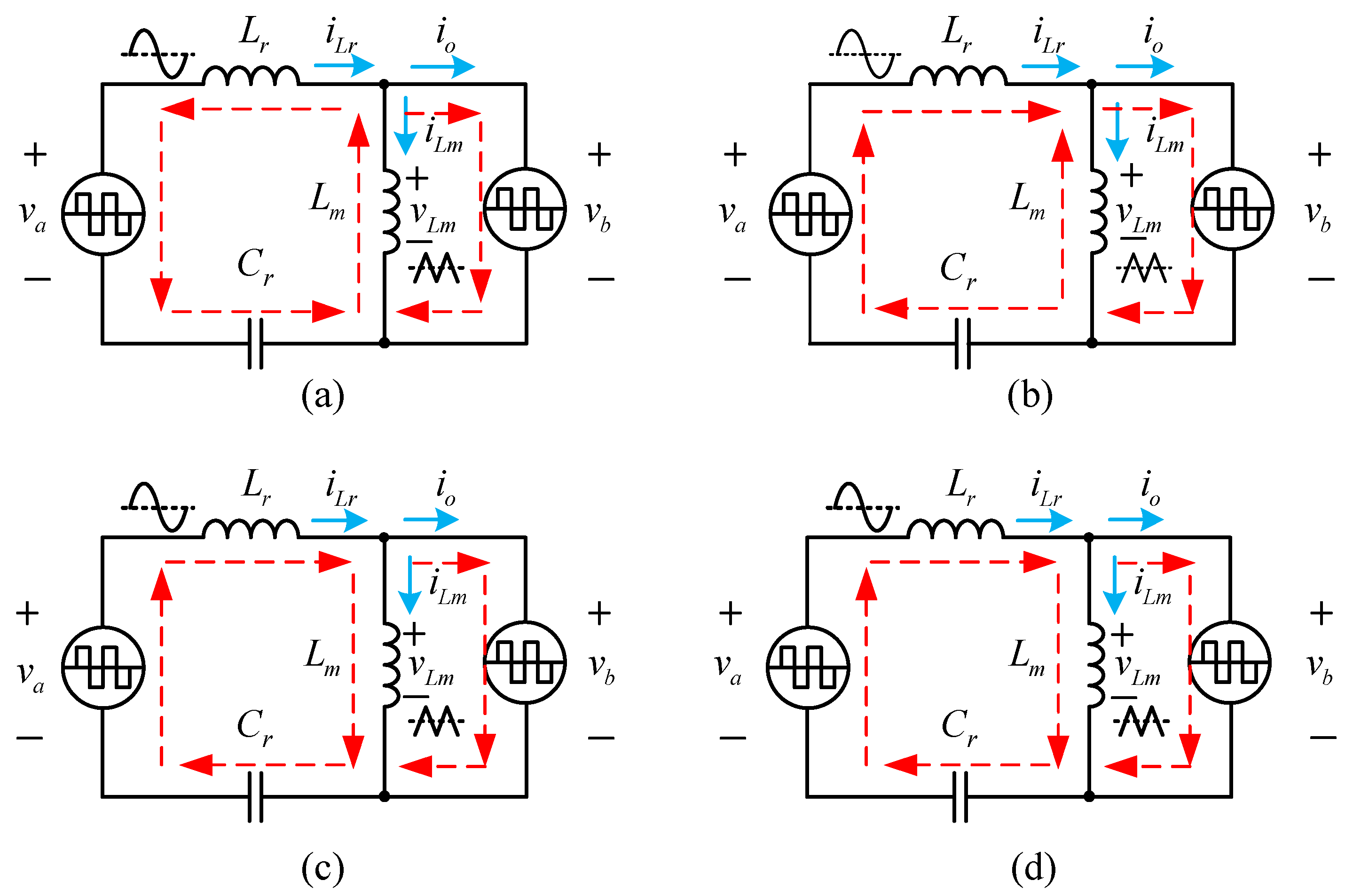
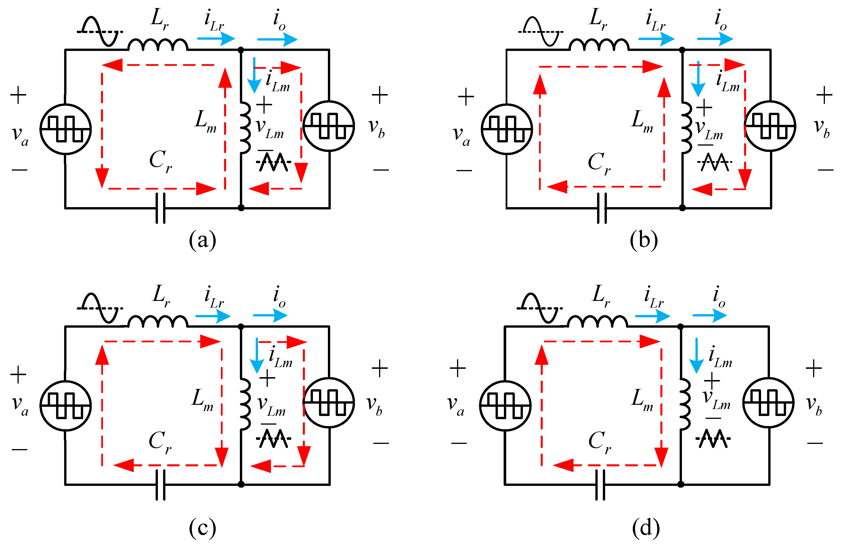
Figure 10 and Figure 11 show the corresponding illustrated waveforms and the accompanying current flows, respectively. There are four operating modes.
Mode 1: [t0tt1]
As shown in Figure 10 and Figure 11a, the voltage va is larger than the voltage vb. Since the voltages va and vLm are positive, the resonant current iLr and the magnetizing current iLm are negative with sinusoidal and linear rise, respectively. At t = t1, this mode ends at iLr = 0, proceeding to Mode 2.
Mode 2: [t1tt2]
As shown in Figure 10 and Figure 11b, the resonance current iLr is positive and increases sinusoidally, while the magnetization current iLm is negative and increases linearly. At t = t2, this mode ends at iLm = 0, proceeding to Mode 3.
Mode 3: [t2tt3]
As shown in Figure 10 and Figure 11c, the resonant current iLr and the magnetizing current iLm are both positive with sinusoidal and linear rise, respectively. At t = t3, the input voltage va reverses and becomes negative, and this mode ends, proceeding to Mode 4.
Mode 4: [t3tt0 + Ts/2]
As shown in Figure 10 and Figure 11d, the resonance current iLr decreases until it equals the magnetization current iLm. At t = t0 + Ts/2, iLr = iLm, this mode ends, proceeding to Mode 1.
When the circuit operates at fs > fr1, the voltage va reverses polarity before the current io naturally reaches zero, causing the rectifier diode to be turned off with relatively high voltage across it due to di/dt, which results in a relatively large reverse recovery current of the diode, thereby increasing switching losses and sacrificing efficiency. In addition, the high diode di/dt turn-off will generate additional voltage stress on the diode, thereby reducing the circuit reliability. For these reasons, the operation at fs > fr1 is undesirable compared with the operation Cases 1 and 2, which should be avoided.

Case 3: Switching Frequency Less than Resonant Frequency (fs < fr1)

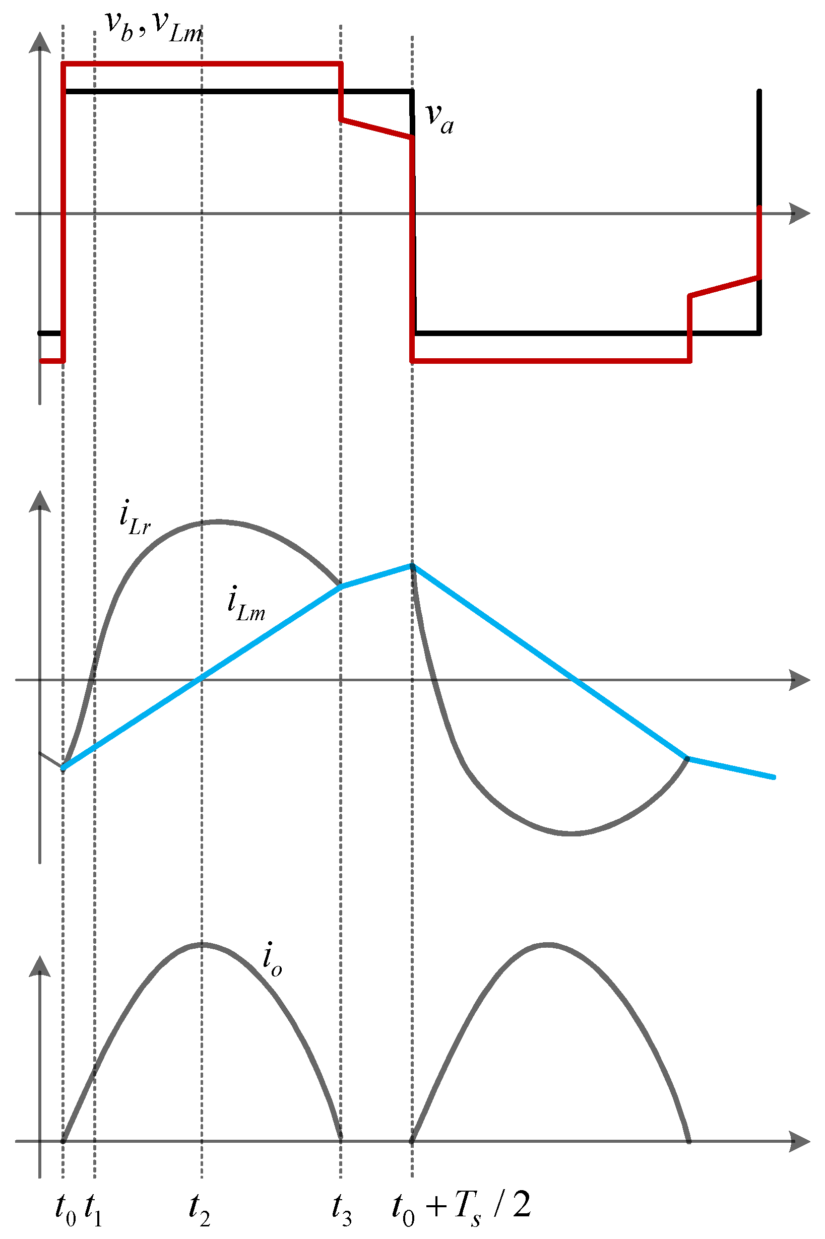
Figure 12 and Figure 13 show the corresponding illustrated waveforms and the accompanying current flows, respectively. There are four operating modes.
Mode 1: [t0tt1]
As shown in Figure 12 and Figure 13a, the voltage vb is larger than the voltage va. Since the voltages va and vLm are positive, the resonant current iLr and the magnetizing current iLm are negative with sinusoidal and linear rise, respectively. At t = t1, this mode ends at iLr = 0, proceeding to Mode 2.
Mode 2: [t1tt2]
As shown in Figure 12 and Figure 13b, the resonance current iLr is positive and increases sinusoidally, while the magnetization current iLm is negative and increases linearly. At t = t2, this mode ends at iLm = 0, proceeding to Mode 3.
Mode 3: [t2tt3]
As shown in Figure 12 and Figure 13c, the resonant current iLr and the magnetizing current iLm are both positive with sinusoidal and linear rise, respectively. At t = t3, this mode ends at iLr = iLm, proceeding to Mode 4.
Mode 4: [t3tt0 + Ts/2]
As shown in Figure 12 and Figure 13d, during this state, io = 0 and iLr = iLm with linear rise. At t0 + Ts/2, the input voltage va reverses and becomes negative, and this mode ends, proceeding to Mode 1.
The operation with fs < fr1 differs in one respect from the operation with fs = fr; the output rectifier current io is discontinuous.

2.2. Backward Boost-Type Energy Transfer

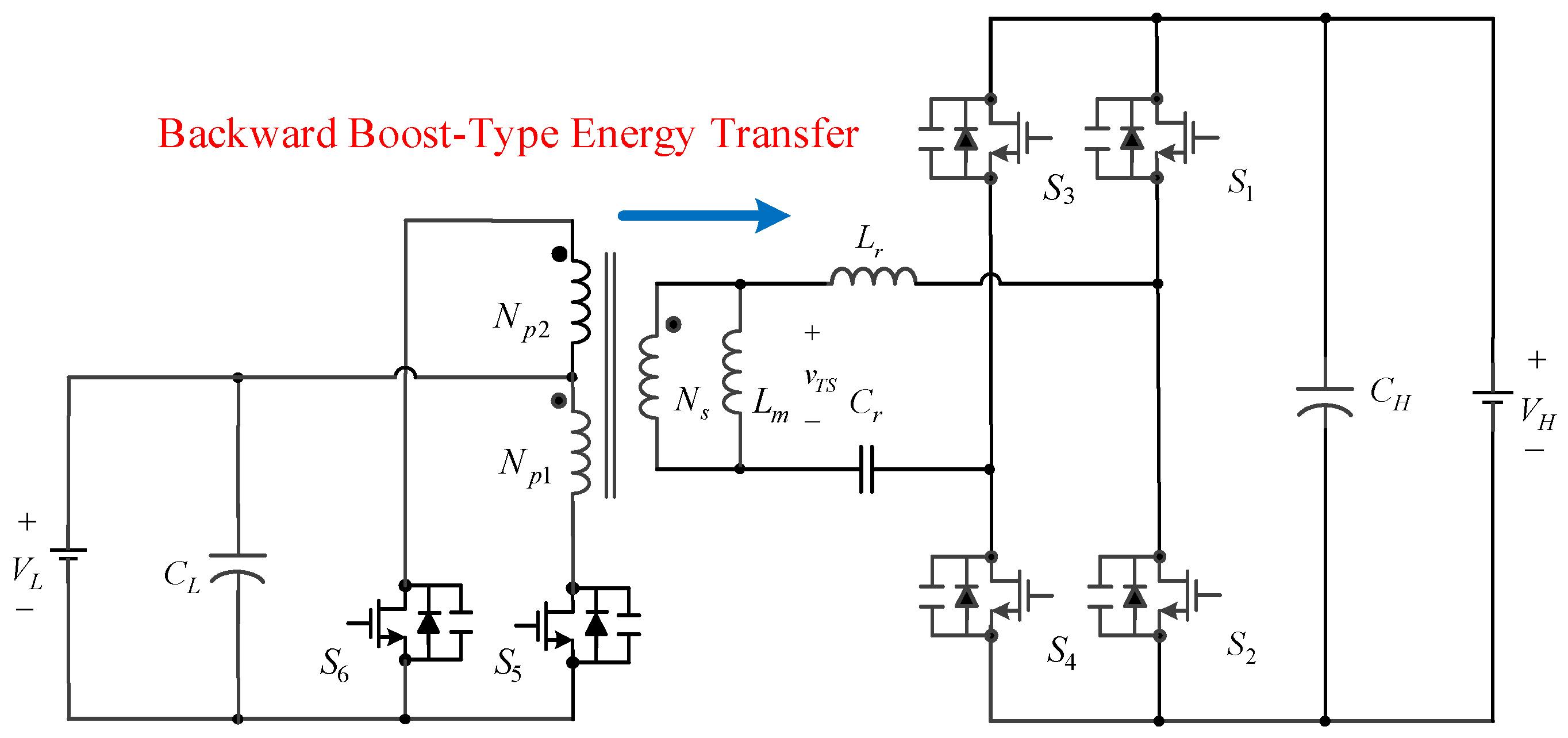
Figure 14 illustrates the high-voltage gain zero-voltage switching (ZVS) push–pull resonant converter. The main circuit consists of a power switch, a high-frequency center-tap transformer, a resonant circuit, a full-bridge rectifier, and an output capacitor. The zero-voltage switching push–pull resonant converter consists of bidirectional switches S5 and S6 with a duty period of nearly 0.5. The resonant inductor Lr is built by the secondary-side leakage inductor and connected with the resonant capacitor Cr to form a resonant tank. However, the magnetizing inductance of a high-frequency transformer is considerable. Consequently, the magnetizing current is negligible. The series resonant circuit is fed from the square wave output voltage on the secondary side of this transformer. The Lr and Cr waveforms are converted into a sinusoidal current for soft-switching operation. The full-bridge rectifier makes the output voltage equal to the peak output value of this transformer by means of a high-capacitance filter capacitor CH. Therefore, the output voltage VH can be regarded as constant. The regulation of the output current is controlled by the change in the duty cycle of the switching period.

2.2.1. Series Load Resonant Converter Analysis

The proposed LC-SRC resonant converter is designed to reduce electromagnetic interference and harmonic distortion because the inductive reactance of the inductor is equal to the capacitive reactance in the resonant case, thereby generating the resonant frequency. In resonant frequency operation, the resonant tank impedance is minimized, and the resonant circuit is used to create a sinusoidal output current. In addition, the characteristic impedance of the resonant circuit is defined as Zr in Equation (24), and its resonant angular frequency is defined as ωr in Equation (25)
Z r = L r C r
ω r = 1 L r C r
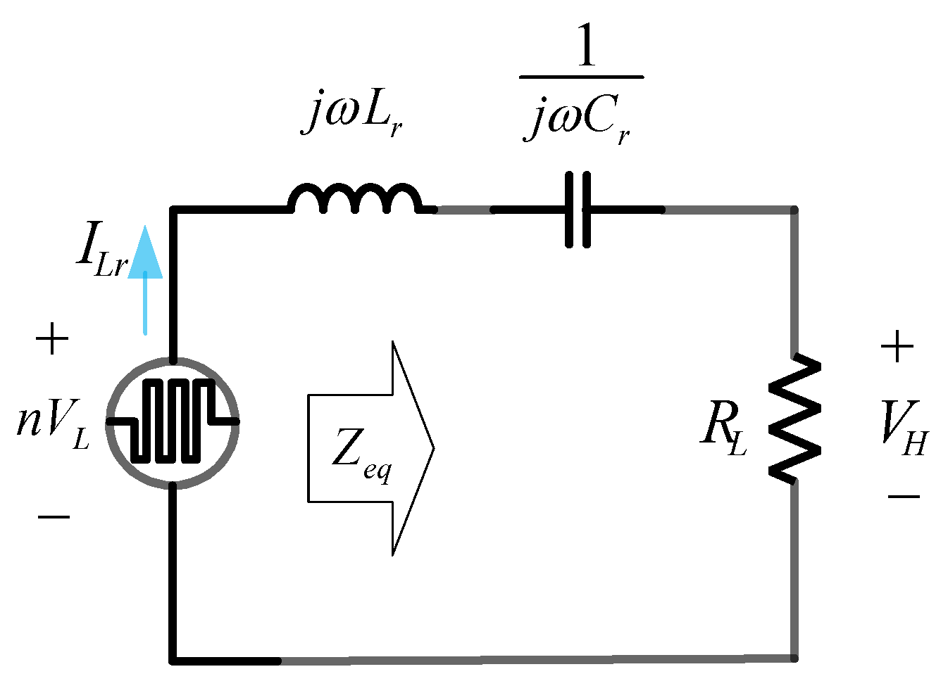
As shown in Figure 15, the load resistor RL is connected in series with the resonant tank to form a series resonant circuit with an inductor Lr, a capacitor Cr, and a resistor RL. If the frequency of the secondary-side output square wave voltage is fs, the series resonant circuit has a filtering function, allowing only the fundamental current to pass. In addition, the turns ratio is n.
The equivalent impedance Zeq of the resonant circuit, viewed from the input voltage to the right, is shown in Equation (26) as
Z e q = R L + j ( ω L r 1 ω C r )
The magnitude and phase of Zeq are shown in Equations (27) and (28), respectively:
Z e q = R L 2 + ( ω L r 1 ω C r ) 2
θ Z e q = θ v θ i = tan 1 ( ω L r 1 ω C r R L )

2.2.2. Voltage Gain

The ratio of the output voltage VH to the input voltage nVL in a series resonant circuit called voltage gain, is shown in Equation (28):
V H n V L = R L R L 2 + ( ω s L r 1 ω s C r ) 2
ω s = 2 π f s
The quality factor Q is defined by Equation (31):
Q = ω r L r R L = 1 ω r R L C r = L r C r R L
ω r = 2 π f r = 1 L r C r
In Equation (32), fr is the resonant frequency of the series resonant circuit, so that the voltage gain can be expressed as Equation (33):
V H n V L = 1 1 + Q 2 ( ω r ω s ω s ω r ) 2
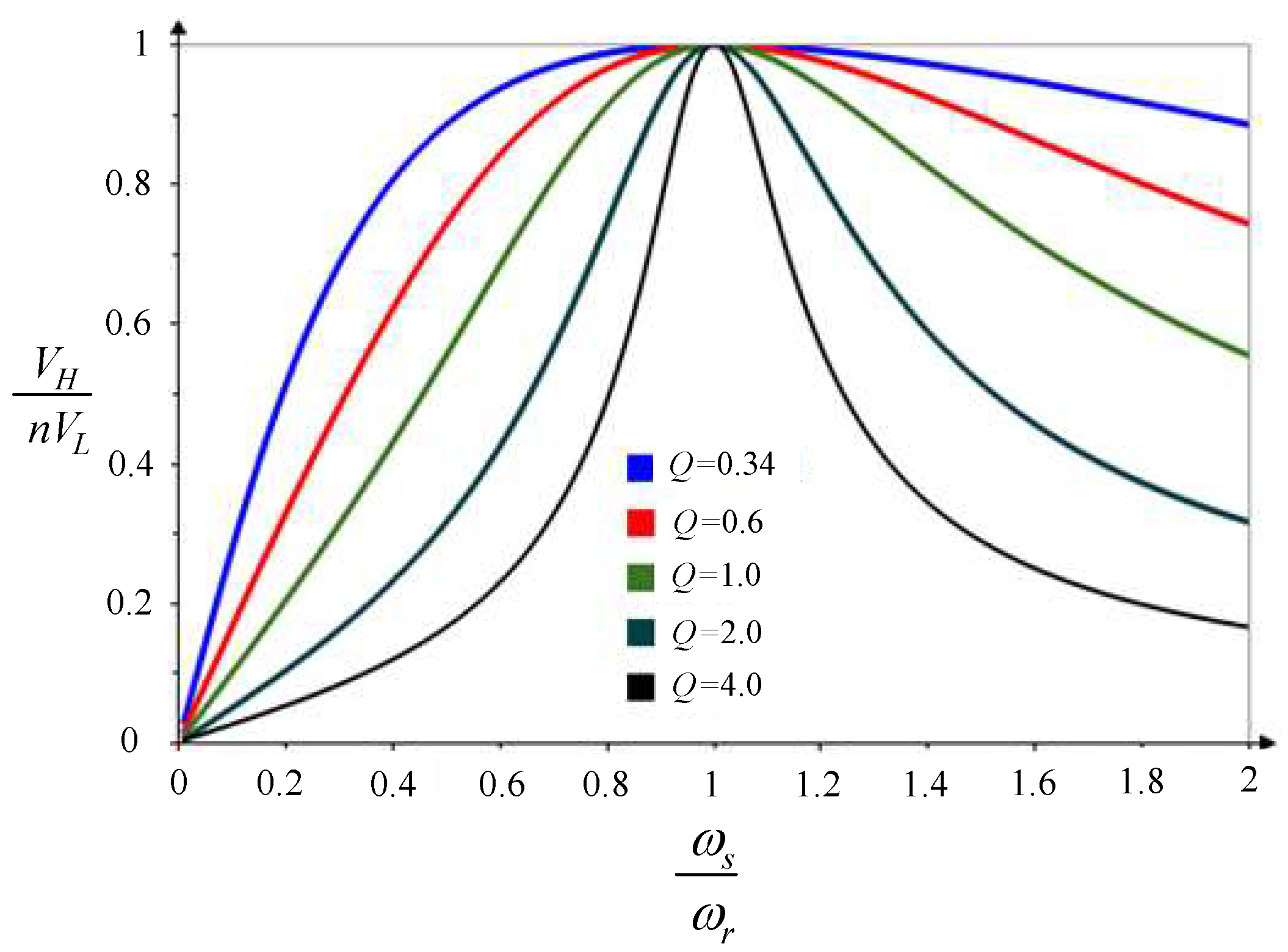
As shown in Figure 16, the relationship between the output–input ratio and the normalized frequency of the series resonant circuit is plotted by different quality factors of Q. Under given values of VL and ωs, the higher the quality factor Q, the smaller the voltage across the load resistor, so reducing the inductance Lr and increasing the capacitance Cr can reduce the quality factor Q to increase the output voltage and keep it close to one.

2.2.3. Operating Principles

The backward boost-type push–pull converter, shown in Figure 14, consists of a push–pull converter and a full-bridge rectifier. The switching frequency fs of the resonant converter is operated at the series resonant frequency fr so that the resonant circuit is reviewed as a high-frequency filterer, and after this filter, the full-bridge rectifier is used to generate the required DC output voltage. The switches S5 and S6 have duty cycles of nearly 0.5, and only the waveforms within 0.5 Ts are considered. Figure 17 and Figure 18 show the corresponding illustrated waveforms and the accompanying current flows, respectively. There are six operating modes.
Mode 1: [t0tt1]
As shown in Figure 17 and Figure 18a, vTS is positive, equal to nVL. During this blanking time, the magnetizing current iLm charges the parasitic capacitance of the switch S6 to double the input voltage VL and discharges the parasitic capacitance of the switch S5 to zero; the body diode of S5 is conducted, and then S5 can be turned on with ZVS. The current in the secondary-side magnetizing inductance Lm called iLm, increases linearly as in Equation (34):
i L m ( t ) = i L m ( t 0 ) + ( v T S / L m ) t
Mode 2: [t1tt2]:
As shown in Figure 17 and Figure 18b, vTS is still positive. During this blanking time, the voltage across the switch S6 is double the input voltage VL. Since the switch S5 is turned with ZVS at t1, the input voltage VL is applied to the primary-side winding Np1, and the corresponding duration is about one-half of the switching cycle. During this mode, iLm is negative and linearly rising, and the power is transferred through the transformer to the DC output on the secondary side. Thus, the voltage across the resonant capacitor Cr, called vCr, is expressed by Equation (35), the voltage across the resonant inductor Lr, called vLr, is expressed by Equation (36), the sinusoidal current io is expressed by Equation (37), and the secondary-side current is is expressed by Equation (38). At t = t2, this mode ends iLm = 0, proceeding to Mode 3:
v C r ( t ) = v C r ( t 1 ) cos ω r ( t t 1 )
v L r ( t ) = ( v T S v H ) v C r ( t 1 ) cos ω r ( t t 1 )
i o ( t ) = [ v T S v H v C r ( t 1 ) ] Z r sin ω r ( t t 1 )
i s ( t ) = i o ( t ) + i L m ( t )
Mode 3: [t2tt3]:
As shown in Figure 17 and Figure 18c, the converter operation in this mode is the same as that in Mode 2 except that iLm is positive and linearly rising, and once the switch S5 is turned off with relatively low current, proceeds to Mode 4. During Mode 3, iLm is linearly falling as in Equation (39):
i L m ( t ) = ( v T S / L m ) t
Mode 4: [t3tt4]:
As shown in Figure 17 and Figure 18d, vTS is negative and equal to −nVL, so iLm is linearly falling. During this blanking time, the magnetizing current iLm charges the parasitic capacitance of the switch S5 to double the input voltage VL and discharges the parasitic capacitance of the switch S6 to zero. If the body diode of S6 is conducted, then S6 can be turned on with ZVS. Once the switch S6 is turned on, this mode proceeds to Mode 5. During this mode, the calculation for iLm linearly falling is expressed by Equation (40) as
i L m ( t ) = i L m ( t 3 ) ( v T S / L m ) t
Mode 5: [t4t5]:
As shown in Figure 17 and Figure 18e, vTS is still negative. During this blanking time, the voltage across the switch S5 is double the input voltage VL. Since the switch S6 is turned with ZVS at t4, the input voltage VL is applied to the primary-side winding Np2, and the corresponding duration is about one-half of the switching cycle. During this mode, iLm is positive and linearly falling, and the power is transferred through the transformer to the DC output on the secondary side. Thus, the voltage across the resonant capacitor Cr called vCr is expressed by Equation (41), the voltage across the resonant inductor Lr is called vLr, is expressed by Equation (42), the sinusoidal current io is expressed by Equation (43), and the secondary-side current is is expressed by Equation (44). At t = t2, this mode ends iLm = 0, proceeding to Mode 3:
v C r ( t ) = v C r ( t 4 ) cos ω r ( t t 4 )
v L r ( t ) = ( v T S v H ) v C r ( t 4 ) cos ω r ( t t 4 )
i o ( t ) = [ v T S v H v C r ( t 4 ) ] Z r sin ω r ( t t 4 )
i s ( t ) = i o ( t ) + i L m ( t )
Mode 6: [t5 ≤ t ≤ t0 + Ts]:
As shown in Figure 17 and Figure 18f. The converter operation in this mode is the same as in Mode 5 except that iLm is negative and linearly falls once the switch S6 is turned off with a relatively low current, operating in Mode 1. During this mode, the calculation for iLm is linearly falling as expressed by Equation (45):
i L m ( t ) = ( v T S / L m ) t

3. Design Procedure for Bidirectional Converter

In the designing process for the forward buck-type forward energy-transferring mode, the high-voltage DC bus was defined as the input voltage, and for the boost-type backward energy-transferring mode, the low-voltage DC power supply created by the storage system was defined as the output voltage. Therefore, the first step was the design of the forward buck-type converter, followed by the design of the backward boost-type converter. Finally, the values of the commonly used components of these two modes were adjusted to meet the required specifications for the bidirectional operation.

3.1. Forward Converter Design

3.1.1. Transformer Turns Ratio Determination

The turns ratio of the transformer was calculated when the voltage gain M is 1 under the normal input condition. Therefore, the turns ratio should satisfy the following Equation (46):
n = M × V H _ n o m V L _ n o m   at   M = 1
where VH_nom is the nominal input voltage, and VL_nom is the nominal output voltage.

3.1.2. Magnetizing Inductance Lm Design

Since the switch loss is related to the magnetizing inductance Lm, the larger the magnetizing inductance is, the smaller the on-state loss. In addition to the turn-on loss, the turn-off loss also depends on the turn-off current, which is equal to the magnetizing current iLm when the switching frequency is less than or equal to the resonance frequency, so a larger excitation inductance Lm can reduce the turn-off loss. In addition, the dead time needs to be increased to ensure ZVS. How to fully discharge the MOSFET’s Coss junction capacitance during the dead time to secure ZVS condition is shown in Equation (47), where the magnetizing current iLm at the end of the dead time is equal to the peak magnetizing current iLm,peak:
i L m , p e a k × t d e a d = 2 × C e q × V H _ n o m
Also, iLm can be expressed by Equation (48):
i L m = V H _ n o m   × T 4 × L m
where T is the switching period equal to the resonant period, tdead is the time interval under the condition that two switches are both in the off state, Ceq is the output capacitance of the MOSFET, and VH_nom is the DC input voltage of the LLC converter. From Equation (48), Equation (49) should be satisfied as
L m < T × t d e a d 8 × C e q

3.1.3. Determining Resonant Circuit Equivalent Load Resistance Rac

As the nominal output voltage and load are determined, the equivalent AC load resistance Rac on the secondary side of the transformer is defined in Equation (50) as
R a c = 8 × ( n π ) 2 × ( V L _ n o m I L _ n o m )

3.1.4. Designing Resonant Inductance Lr and Capacitance Cr

To achieve load regulation over the entire operating range, the design must satisfy the values of Q and λ (λ = Lr/Lm) for the maximum voltage gain. Figure 6 shows that the lower the value of Q is, the higher the maximum voltage gain, whereas in Figure 7, it is evident that the higher the value of λ is, the higher the maximum voltage gain. For a given value of the resonant frequency fr, increasing λ means decreasing the magnetizing inductance Lm, which increases the circulating current. Therefore, there is a compromise between the range of the available voltage gain and the conduction losses. Once the magnetizing inductance Lm is chosen, the relationship between the values of Q and λ, as defined by Equation (51), can be calculated as
Q λ = 2 × π × f r R a c × L m
Therefore, the ratio of Q to λ was also determined for the designed magnetizing inductor Lm. A relatively large λ and a relatively small Q are usually preferred to obtain a relatively wide switching frequency operating range, and a value of λ between 0.25 and 0.1 is usually recommended.
L r = λ × L m
The value of Lr can be obtained based on Equation (52), and substituting this value into Equation (53) obtains the value of Cr as
C r = 1 ( 2 × π × f r ) 2 × L r
The value of Q can be obtained by substituting Equations (50), (52) and (53) into Equation (54) as
Q = L r / C r R a c

3.1.5. Transformer T Design

The primary-side and secondary-side turns, because of the output voltage being clamped, can be easily deduced from the primary-side turns Np as in Equation (55)
N p = V L _ n o m 4 × f r × B m × A e
where VL_nom is the nominal DC output voltage, Bm is the maximum flux density, and Ae is the magnetic core area.
Since the Ns is the turns ratio n times Np, based on Equation (56), the turns of Ns can be obtained by
N s = n × N p

3.2. Backward Converter Design

Because the topology proposed in this paper belongs to the bidirectional DC–DC converter, the circuit operations of the two converters use the same resonant circuit. Thus, the design of the two components should have the same parameters, but because of the different topologies, the design of the component parameters should comply with the established specifications to achieve a compromise in design. Since the detailed design of the forward buck-type LLC resonant converter is already explained, the values of its components have been designed to ensure a wide input voltage range. The following is the parameter design and calculation of a push–pull resonant converter. Since the backward boost-type push–pull resonant converter is mainly operated at the resonant point, the output voltage modulation was controlled by the PWM strategy. The maximum duty cycle, called Dmax, was chosen to be less than 0.5, so the turns ratio n of the transformer is given in Equation (57):
n = V H _ n o m 2 × V L _ n o m × D m a x
The backward boost-type push–pull resonant converter is supplied with an appropriate AC resistance after the rectifier, called Rac, at the nominal output voltage and load. This resistance can be defined in Equation (58) as
R a c = 8 π 2 V H _ n o m I H _ n o m
In the design procedure, choosing the switching frequency fs equal to the resonant frequency fr was adopted. As shown in Figure 16, choosing a smaller Q curve can achieve a smoother curve of the voltage-boosting gain.
Next, the values of the resonant components can be calculated, and hence, the values of Lr and Cr can be solved using Equations (59) and (60)
C r = 1 2 π f r R a c Q
L r = 1 ( 2 π f r ) 2 C r
From Equation (58) to (60) mentioned above, the validation of the backward boost-type push–pull converter is similar to that of the forward buck-type LLC converter with respect to important components. Therefore, it can be shown that the same set of components of the resonant circuit can be used for different control methods on different structures of the bidirectional converter.

4. Battery Charge/Discharge Control Method

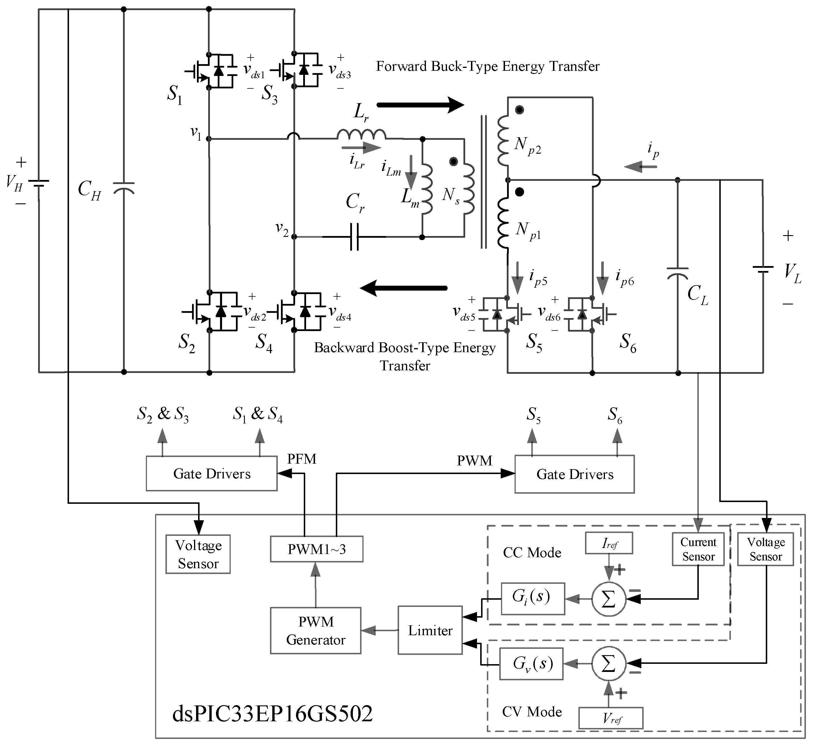
At present, battery charging methods, including constant-current (CC) mode, constant-voltage (CV) mode, constant-current constant-voltage (CC–CV) mode, and pulse mode, are commonly used. Among these methods, the CC–CV mode is the most preferable. The control framework of the proposed bidirectional LLC full-bridge resonant converter for charging and discharging modes is shown in Figure 19 and consists of two main parts. The first part comprises the power converter based on the full-bridge LLC resonant circuit, whereas the second part is built by the digital control circuit based on the dsPIC microcontroller. The first part was explained in detail earlier, so this section focuses on the design of the digital controller and the software-planning process. For the forward buck-type energy transfer, the voltage and current of the power converter were detected so that a pulse frequency modulation (PFM) signal to control the switching frequency of the switches S1 to S4 was created. At the same time, the switches S5 and S6 were turned off so that the low-voltage output was rectified by the body diodes of the switches S5 and S6. For the backward boost-type energy transfer, a pulse width modulation (PWM) signal was generated so that the duty cycles of the switching frequency for S5 and S6 were controlled. At the same time, the switches S1 to S4 were turned off so that the high-voltage output was rectified by the body diodes of the switches S1 to S4.

4.1. Software Planning Process

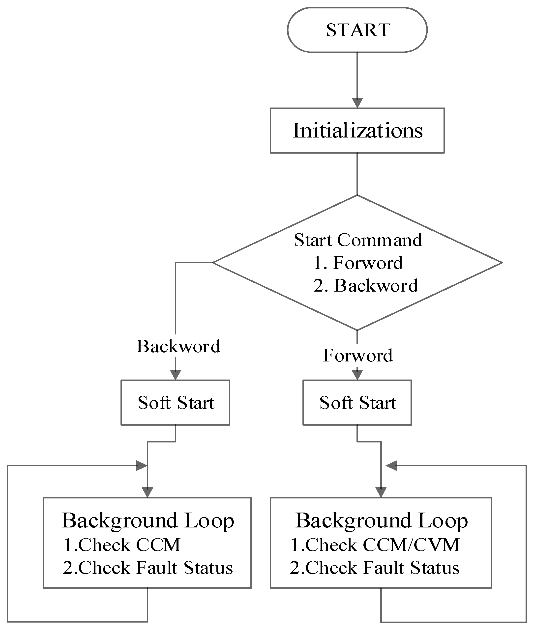
The MPLAB X IDE v6.00 software planning process is mainly divided into three parts. The first part is the main program shown in Figure 20 as a block diagram. In this part of the code, all the primary system operations and peripheral interfaces were initialized at the beginning. The switching operation of the forward buck charging behavior belongs to the PFM frequency control of the LLC full-bridge converter, which was designed to use one set of PWM1 channels containing two signals, PWM1H and PWM1L. The PWM1H drives the high-voltage-side switch S1 of the secondary-side forearm half-bridge leg and the low-voltage-side switch S4 of the secondary-side rear-arm half-bridge leg. PWM1L drives the low-voltage-side switch S2 of the secondary-side forearm half-bridge leg and the low-voltage-side switch S3 of the secondary-side rear-arm half-bridge leg. The backward boost discharge behavior belongs to the PWM duty cycle control for the push–pull converter designed to use one set of PWM3 channels containing two signals, PWM3H and PWM3L, which drives the primary-side switches S5 and S6, respectively. According to the literature [30], since the voltage source is embedded in the DC grid, the converter will be unstable when the converter is controlled under the constant voltage output. Therefore, the discharge mode proposed in this paper sets the battery to be discharged in a constant current mode according to the battery voltage to avoid the battery discharging under a high current at a low state of charge (SOC), resulting in reducing the battery temperature and increasing the battery life. When the converter was operated in the forward buck charging mode, the background loop was used to determine the status of the constant current mode/constant voltage mode and detect the fault status. When the converter was switched to the backward boost discharge mode, the background loop detected the battery voltage to set the reference value for the constant current output and the fault status.

4.2. Forward Charge Mode

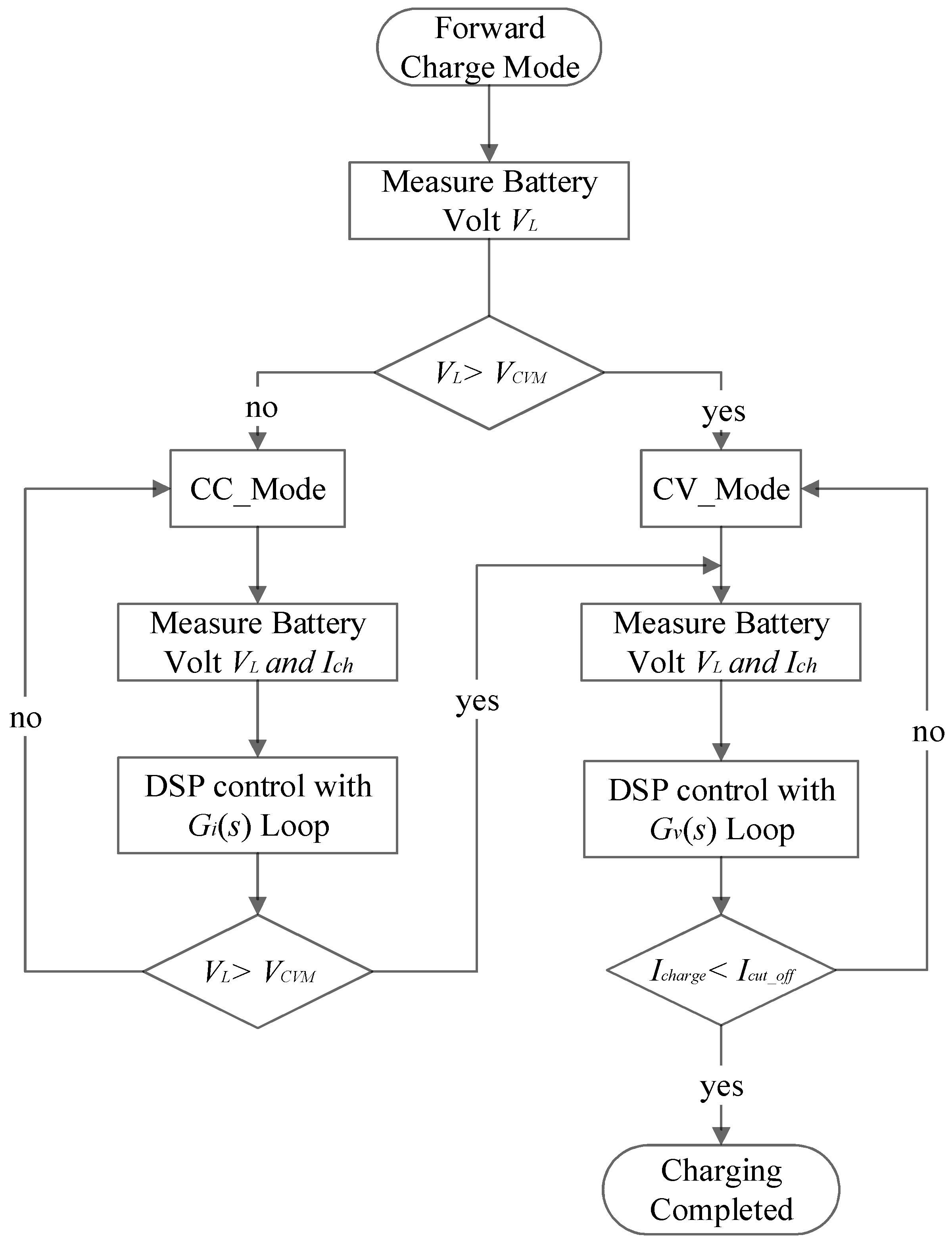
The second part of the code is the flowchart of the CC–CV mode control software for the forward buck LLC full-bridge resonant converter charging mode, as shown in Figure 21. The current sensor measured the battery charging current Ich and subtracted the battery charging current Ich from the reference current Iref to obtain the error value. After this, a proportional integral controller was used to calculate the compensation value for this error, and a PFM signal was obtained from the compensation value to drive the switches S1 to S4 to realize constant current charging. When the converter operated in constant current charging mode, the DSP digital control circuit continued to detect the battery voltage. If the battery voltage reached the preset value of the constant voltage mode VCVM, the converter switched to the CV charging mode. Therefore, the voltage sensor measured the battery voltage VL and obtained an error value by subtracting the battery voltage VL from the reference voltage Vref. Afterward, a proportional integral controller was used to calculate the compensation value for this error, and a PFM signal was obtained from the compensation value to drive the switches S1 to S4 to realize output constant voltage charging. When the converter was switched to CV charging mode, the DSP digital control circuit continued to measure the battery charging current Ich. When the battery charging current was less than or equal to the preset battery cutoff current Icut_off, the charging process was completed, and the DSP digital control circuit sent a termination signal to the switches S1 to S4 to turn off the converter.

4.3. Forward-Mode DSP Control ISR

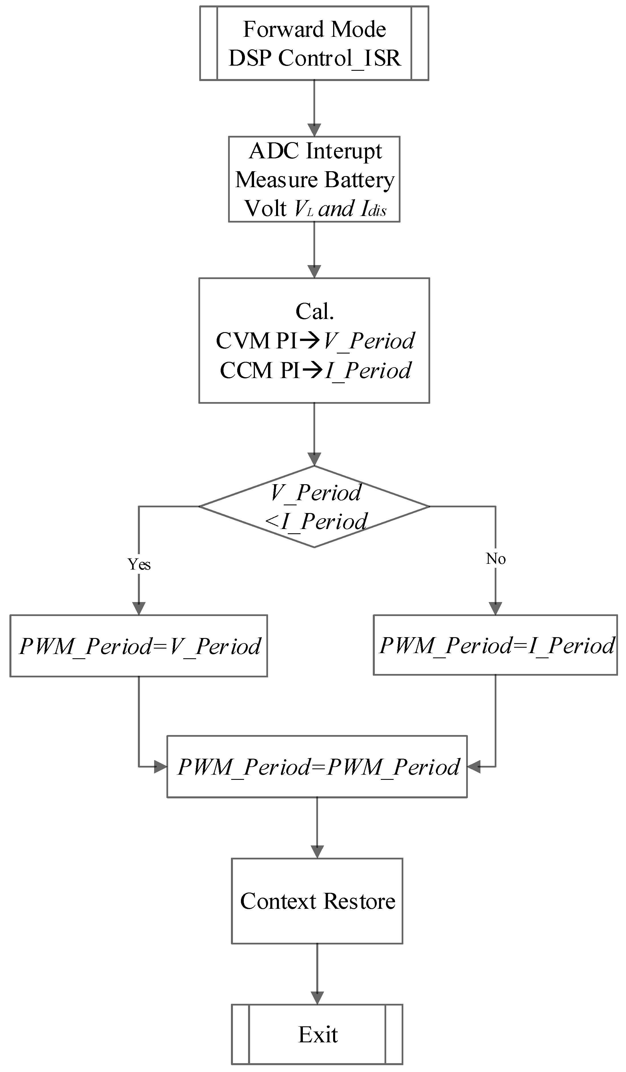
Figure 22 shows the flowchart of forward-mode DSP control ISR, where “ISR” is an abbreviation of “interrupt service routine”. The program entered the ADC interrupt subroutine to obtain information on voltage and current when the interrupt was triggered. Through try and error, the proportional gain kp and integral gain ki in the constant voltage mode (CVM) were set at 0.1 and 0.05, respectively, whereas the values of kp and ki in the constant current mode (CCM) were set at 0.1 and 0.06, respectively. At the same time, the corresponding periods in CCM and CVM were calculated out and compared together. After this, the period in CVM, called V_Period, was compared with the period in CCM, called I_Period, and the smaller one was chosen to control the switches S1 to S4.

4.4. Backward Discharge Mode

The third part of the code is the flowchart of the CC control software for the backward boost push–pull converter discharging mode, as shown in Figure 23. First, the voltage sensor measured the battery voltage VL, and the reference discharge current Idis_ref was set according to the battery voltage VL. At that time, the converter entered the CC mode, the current sensor measured the battery discharge current Idis, and subtracted the reference current Idis_ref from the battery discharge current Idis to obtain the error value. A proportional integral controller was used to calculate the compensation value for this error value, and then the duty cycles of the switching frequency were obtained according to the compensation value to drive the switches S5 and S6 to realize constant current discharge. Simultaneously, the DSP digital control circuit detected the battery voltage VL and then determined whether the battery voltage was less than the battery cutoff voltage Vcut_off. If the battery voltage VL equaled the battery cutoff voltage Vcut_off, the discharge process was terminated. In this case, the DSP digital control circuit stopped sending signals to the switches S5 and S6, thus stopping the converter and preventing damage to the battery.

4.5. Backward-Mode DSP Control ISR

Figure 24 shows the flowchart of backward-mode DSP control ISR. The program entered the ADC interrupt subroutine to obtain information on voltage and current when the interrupt was triggered. Via try and error, the proportional gain kp and integral gain ki in CCM were set at 0.15 and 0.01, respectively. After this, the duty in CCM, called I_Duty, was chosen to control the switches S5 and S6.

5. Experimental Results

First, the operating high-side voltage range of the bidirectional converter was determined to be between 360 V and 410 V for the forward buck mode fed from the high-voltage DC bus, and the low-side voltage range was between 43 V and 52 V for the backward boost mode fed from the low-voltage DC storage source. In this study, a sample 500 W bidirectional full-bridge resonant converter was presented, and its capability of bidirectional power transfer between the low-voltage system and the high-voltage DC bus was verified. The system and component specifications of the converter are listed as described in Table 2.

5.1. Instrumentation Configuration

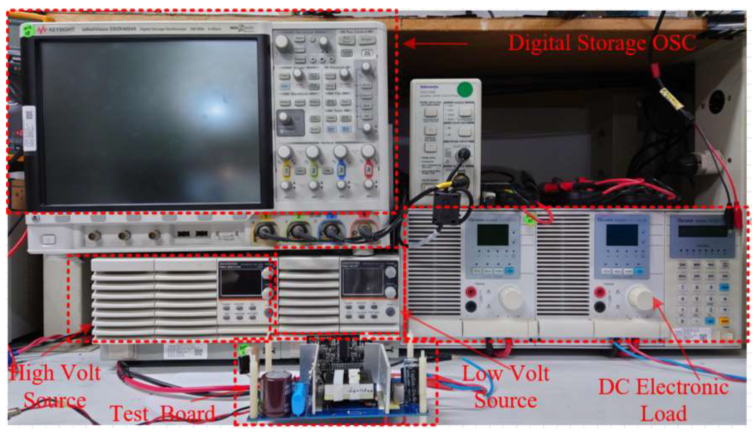
Figure 25 shows the instrumentation configuration for the experimental setup, where High Volt Source (Model: GWINSTEK PSW 800-4.32) supplied the voltage from 360 to 410 V, Low Volt Source (Model: GWINSTEK PSW 80-27) supplied the voltage 43~52 V, DC Electronic Load (Model: Chroma 63308A) provided the output load, and Digital Storage OSC (Model: KEYSIGHT DSOX4024) was used to measure the voltage and current waveforms. Test Board is the proposed prototype circuit. In addition, the measurement condition was that Electronic Load was set at the CV mode for the forward voltage-bucking and backward voltage-boosting operation.
Figure 26 shows the proposed main power stage on the top side and its peripheral circuits, where Aux. Power mainly supplies the operating voltages of the circuit board, such as 12 V for the secondary-side drive circuit, 12 V for the primary-side drive circuit and 5 V for the control board, dsPIC Controller is the control kernel of the circuit operation to measure the voltage and current signals as well as to output the gate driving signals to drive the switches, Lr/T1 is the transformer which integrates the resonant inductor, S1 to S4 are the secondary-side switches, S5 and S6 are the primary-side switches, VH is the high voltage output/input, and VL is the low voltage output/input.
Figure 27 shows the proposed main power stage on the bottom side and its peripheral circuits, where Gate Drivers_H and Gate Drivers_L are the individual drive circuits for the secondary-side high-voltage full-bridge switches and the primary-side push-pull switches, Cr is the resonant capacitor, the Volt Sensor is the isolated voltage detector on the secondary side, and the Current Sensor is the current detector on the primary side.

5.2. Forward Charge Mode

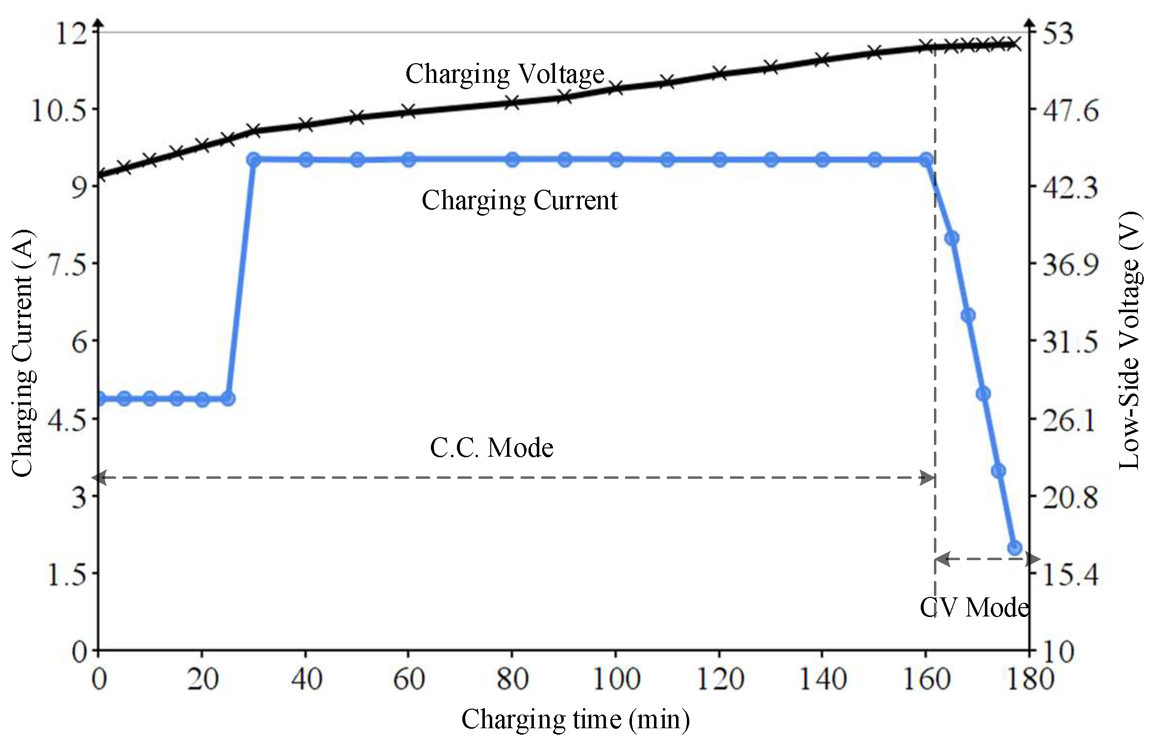
The CC–CV charging mode of the forward buck converter takes a two-stage constant current charging. As shown in Figure 28, the blue color is the constant current charging curve. When the low-side voltage was lower than 46 V, the charging current was a constant current of 5 A. When the low-side voltage exceeded 46 V, the charging current was a constant current of 9.5 A. As shown in Figure 23, the black color is the low-side voltage curve, and the voltage increased with the increase in charging time. When the low-side voltage reached 52 V, it was charged with constant voltage, and the charging current started to decrease.
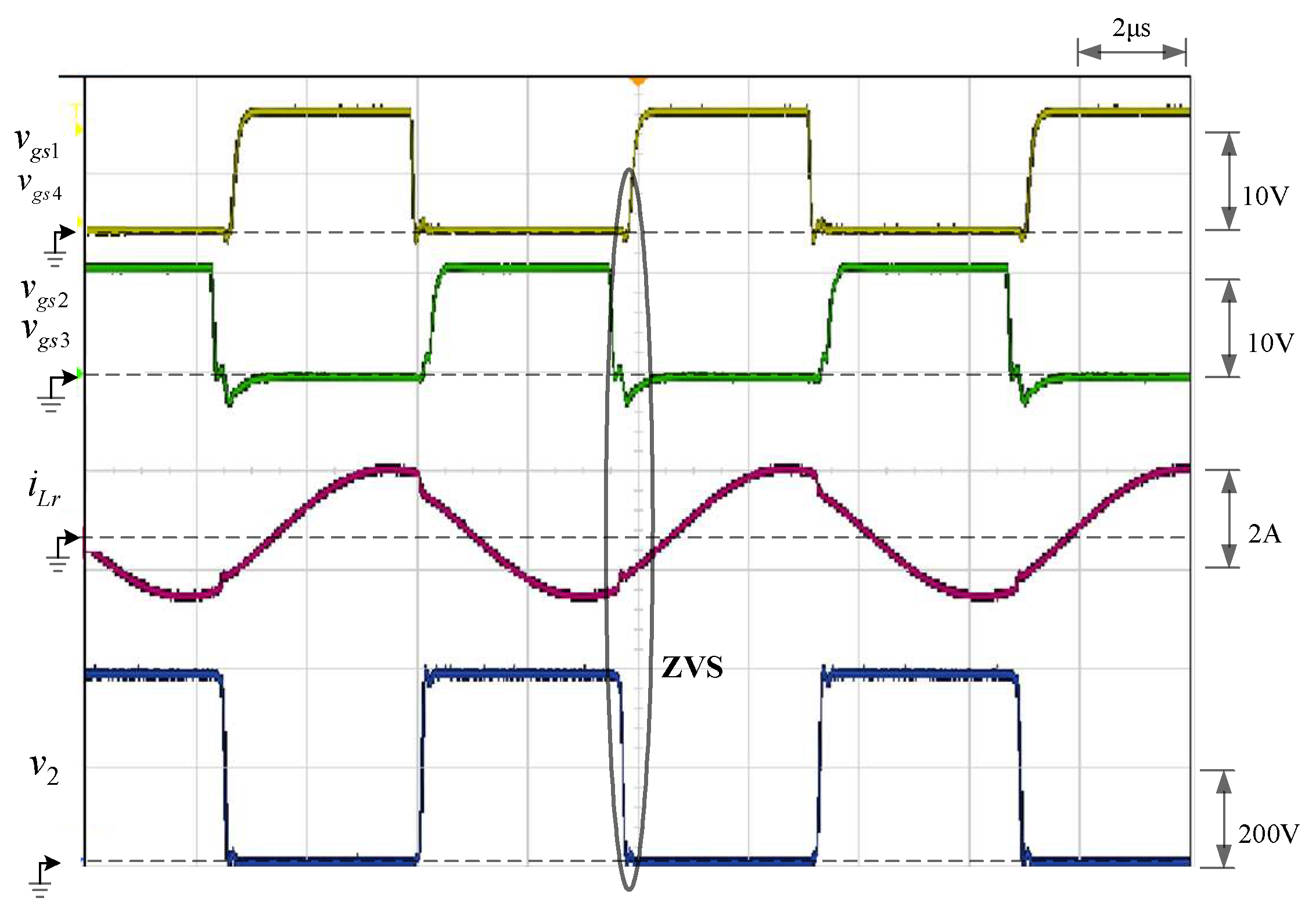
As shown in Figure 29, the waveforms are measured under a high-side input voltage DC bus of 390 V, the charging current is 5 A, the low-side voltage is 45 V, and the corresponding power was 225 W. The yellow curve is the gate drive signals vgs1 and vgs4 for the switches S1 and S4, respectively; the green curve is the gate drive signals vgs2 and vgs3 for the switches S2 and S3, respectively, and the blue curve is the voltage v2, which is the voltage across the switch S4, called vds4. From these waveforms, it can be seen that the switch S4 had a ZVS turn-on. In addition, the switching frequency fs operated at 139.3 kHz, larger than the resonance frequency fr (125 kHz). Accordingly, the resonant inductance current iLr of the red curve was larger than that of iLm at the turn-off of the switch S1.
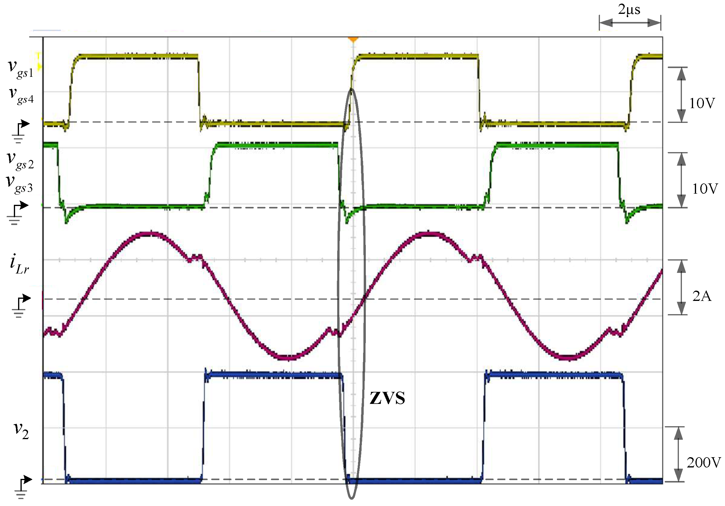
As shown in Figure 30, the waveforms are measured under a high-side input voltage DC bus of 390 V, the charging current was 9.5 A, the low-side voltage is 48 V, and the corresponding power was 450 W. The yellow curve is the gate drive signals vgs1 and vgs4 for the switches S1 and S4, respectively; the green curve is the gate drive signals vgs2 and vgs3 for the switches S2 and S3, respectively, and the blue curve is the voltage v2, which is the voltage across the switch S4, called vds4. From these waveforms, it can be seen that the switch S4 had a ZVS turn-on. In addition, the switching frequency fs operated at 110.3 kHz, which is lower than the resonance frequency fr (125 kHz). Accordingly, the resonant inductance current iLr of the red curve was larger than that of iLm at the turn-off of the switch S1.
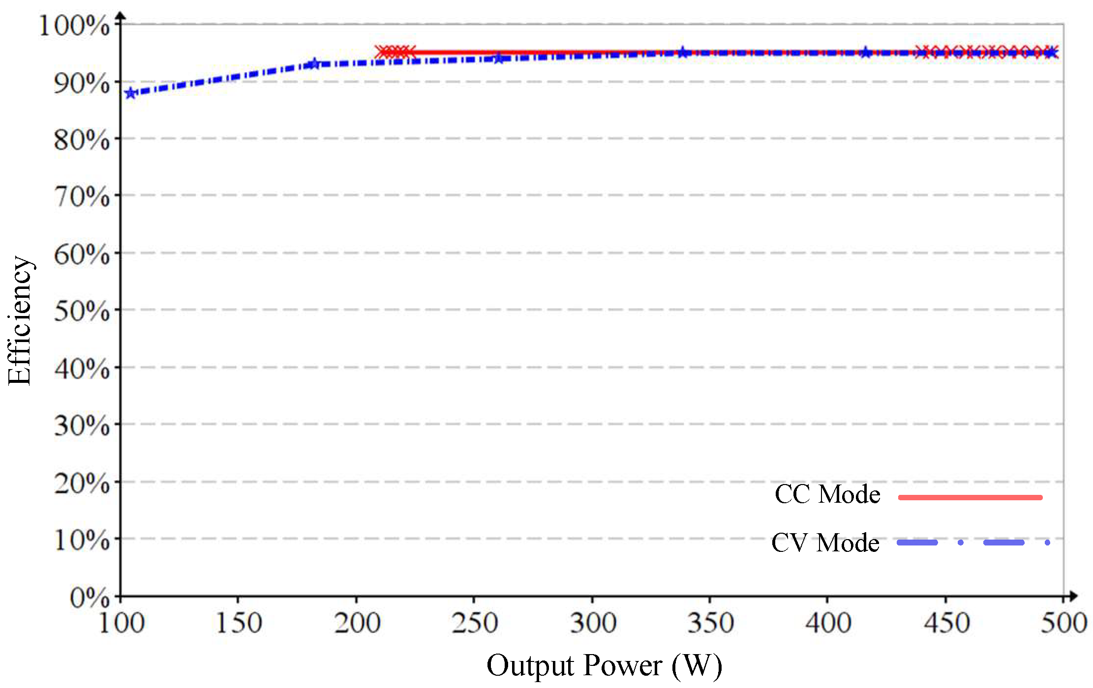
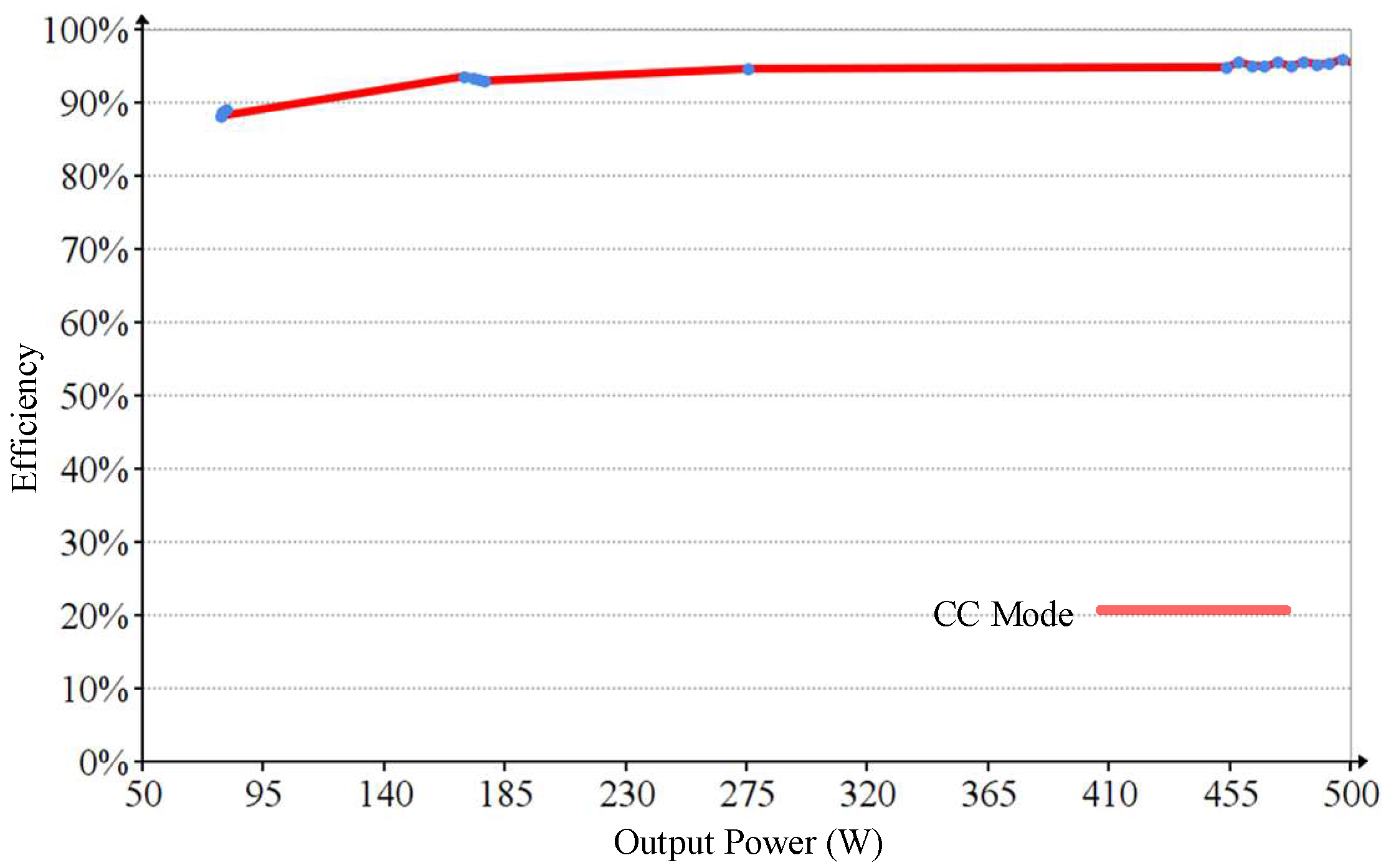
As shown in Figure 31, the efficiency curve of the CC–CV charging mode obtained from the forward buck converter, the red curve shows that the efficiency of the CC charging mode was maintained above 95%, where the output power locates between 215 W and 235 W in the first stage of 5 A charging, and the output power locates between 460 W and 500 W in the second stage of 9.5 A charging. On the other hand, the blue curve shows that the efficiency of the CV charging mode was initially maintained above 95%, drops with the decrease of the output power, and finally drops to 88% when the output power was 100 W.

5.3. Backward Discharge Mode

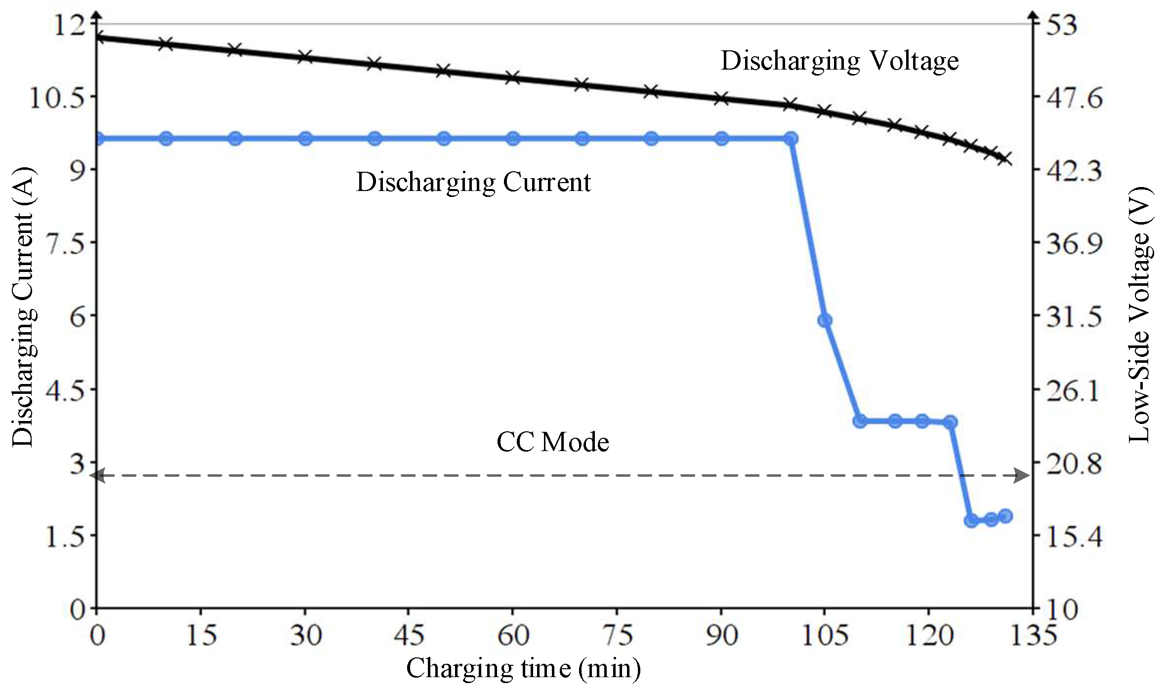
The CC discharge mode of the backward boost converter takes constant current discharge when the low-side source is discharged. As shown in Figure 32, the blue color is the CC discharge curve. When the low-side voltage exceeded 47 V, the low-side source was discharged at a constant current of 9.6 A to the high-voltage DC bus. When the low-side source voltage was between 47 V and 46 V, the low-side source was discharged at a constant current of 6 A to the high-voltage DC bus. When the low-side source voltage was between 46 V and 44.5 V, the low-side source was discharged at a constant current of 4 A to the high-voltage DC bus. When the low-side source voltage was lower than 44.5 V, the low-side source was discharged at a constant current of 2 A to the high-voltage DC bus. As shown in Figure 27, the black color is the curve of the low-side source voltage, and this voltage decreases as the discharge time increases.
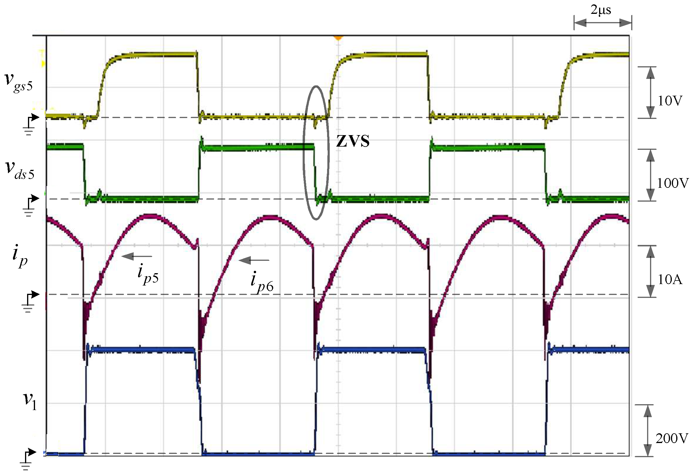
As shown in Figure 33, the high-side output voltage DC bus was 408 V and 493 W, the input constant current of the converter was 9.65 A, and the low-side source voltage was 51 V. The yellow curve is the gate driving signal vgs5 for the switch S5, and the green curve is the voltage across the switch S5, called vds5. The blue curve is the voltage v1, the input voltage of the full-bridge rectifier on the high-voltage side. This figure shows that the switch S5 had a ZVS turn-on, and the PWM switching frequency was 125 kHz with a duty cycle of 0.43.
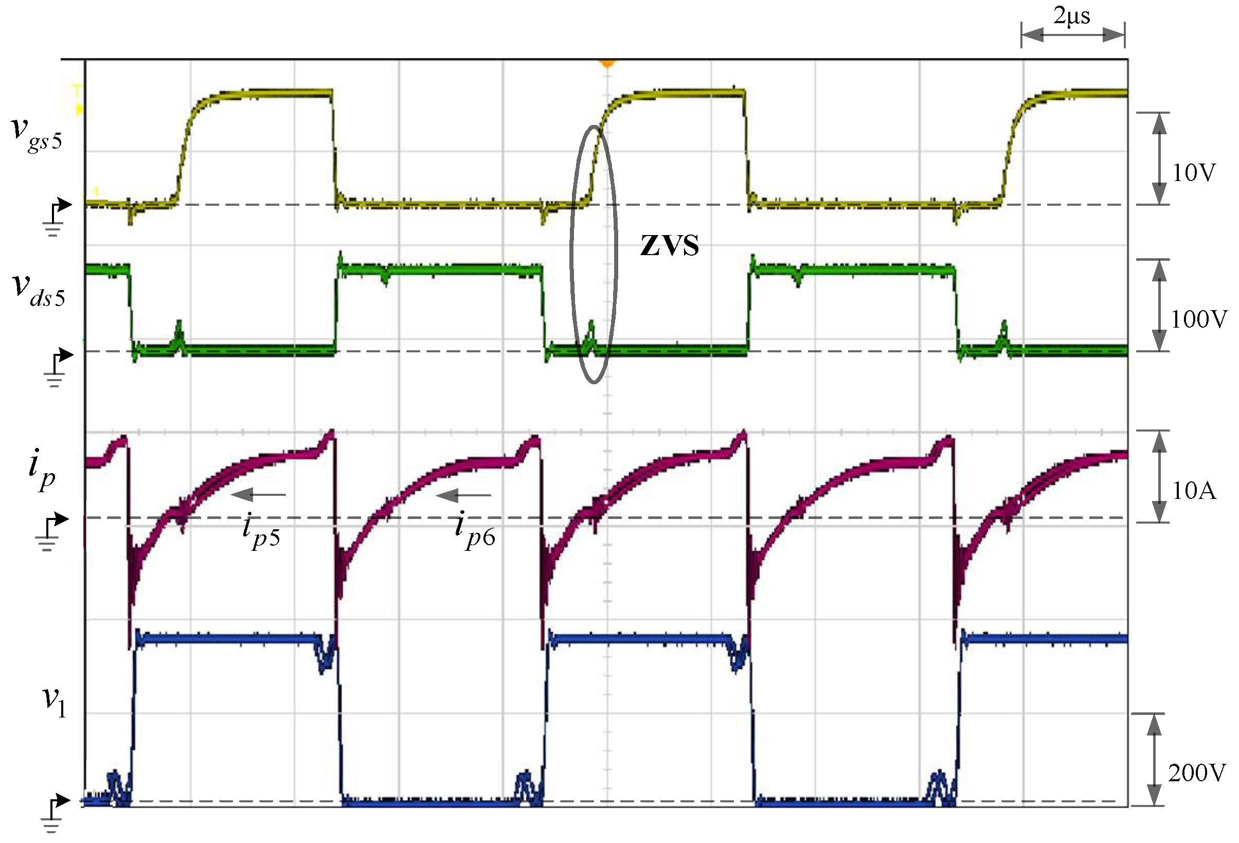
As shown in Figure 34, the high-side output voltage DC bus was 360 V, the power was 170 W, the input constant current of the converter was 4 A, and the low-side source voltage was 44.5 V. The yellow curve is the gate drive signal vgs5 for the switch S5, and the green curve is the voltage across the switch S5, called vds5. The blue curve is the voltage v1, which is the input voltage of the full-bridge rectifier on the high-voltage side. This figure shows that the switch S5 had a ZVS turn-on, and the PWM switching frequency was 125 kHz with a duty cycle of 0.36.
Figure 35 shows the efficiency curve of the CC discharge for the backward boost converter, where the red curve for the efficiency under the CC discharge mode initially maintains more than 95%. The discharge current was determined by the low-side source voltage, and the corresponding output power was concentrated in 450~500 W, 180 W, and 80 W, as shown by blue color. However, the efficiency was reduced to 88% at the output power of 100 W.

5.4. Experimental Summarization

The experimental method adopts CC and CV mode control for forward buck-type energy transfer on the low-voltage side and the CC mode control for boost-type energy transfer on the low-voltage side. Stepwise segmented current charging and discharging techniques are adopted to avoid battery temperature rise caused by high power charging and discharging at low battery capacity, and this will reduce the battery life.

6. Conclusions

This paper proposed a bidirectional control strategy, which performs the bidirectional energy transfer function without changing the topology of the LLC resonant converter. The conventional PFM switching technique was used to control the full-bridge LLC switches for forward buck mode. The push–pull switches were controlled by the PWM switching technique with a variable duty cycle for backward boost mode. The proposed system utilized the resonant tank on the high-side voltage for bidirectional energy transfer, with ZVS on both the input switches and used the battery as the main target in the control strategy. When the battery was charged, there were three charging stages, and when the battery was discharged, the discharge control method was based on the stored energy of the battery (SOC). That is, the battery was discharged with low current at a low voltage to prolong the life of the battery, as well as to minimize temperature rise and internal solid electrolyte interphase (SEI). Furthermore, as compared with Table 1, the proposed converter had an input voltage range of 43–52 V, an output voltage range of 360–410 V, an output power of 500 W, and a maximum efficiency of 95.1%. We used LLC topology, adopted the PFM/PWM control technique, six main switches, and the number of inductors/transformers/capacitors was one each. Accordingly, the proposed control strategy can achieve wide input and output ranges with relatively few components.

Author Contributions

Conceptualization, Y.-K.T. and K.-I.H.; methodology, Y.-K.T. and K.-I.H.; software, Y.-K.T.; validation, Y.-K.T. and K.-I.H.; formal analysis, Y.-K.T. and K.-I.H.; investigation, Y.-K.T.; resources, Y.-K.T.; data curation, Y.-K.T.; writing—original draft preparation, Y.-K.T. and K.-I.H.; writing—review and editing, K.-I.H.; visualization, Y.-K.T.; supervision, K.-I.H.; project administration, K.-I.H.; funding acquisition, K.-I.H. All authors have read and agreed to the published version of the manuscript.

Funding

This research was funded by the Ministry of Science and Technology, Taiwan, under the Grant Number: NSTC 112-2221-E-027-015-MY2.

Data Availability Statement

No new data were created or analyzed in this study. Data sharing is not applicable to this article.

Conflicts of Interest

The authors declare no conflict of interest.

References

  1. Mohtasham, J. Review article-renewable energies. Energy Procedia 2015, 74, 1289–1297. [Google Scholar] [CrossRef]
  2. Lawder, M.T.; Suthar, B.; Northrop, P.W.C.; De, S.; Hoff, C.M.; Leitermann, O.; Crow, M.L.; Santhanagopalan, S.; Subramanian, V.R. Battery Energy Storage System (BESS) and Battery Management System (BMS) for Grid-Scale Applications. Proc. IEEE 2014, 102, 1014–1030. [Google Scholar] [CrossRef]
  3. Rachid, A.; Fadil, H.E.; Gaouzi, K.; Rachid, K.; Lassioui, A.; Idrissi, Z.E.; Koundi, M. Electric vehicle charging systems: Comprehensive review. Energies 2023, 16, 255. [Google Scholar] [CrossRef]
  4. Attar, H.A.; Hamida, M.A.; Ghanes, M.; Taleb, M. LLC dc-dc converter performances improvement for bidirectional electric vehicle charger application. World Electr. Veh. J. 2022, 13, 2. [Google Scholar] [CrossRef]
  5. Al-Ismail, F.S. Dc microgrid planning, operation, and control: A comprehensive review. IEEE Access 2021, 9, 36154–36172. [Google Scholar] [CrossRef]
  6. Lowder, T.; Xu, K. The Evolving U.S. Distribution System: Technologies, Architectures, and Regulations for Realizing a Transactive Energy Marketplace; Technical Report; National Renewable Energy Laboratory: Golden, CO, USA, 2020. [Google Scholar]
  7. Gorji, S.A.; Sahebi, H.G.; Ektesabi, M.; Rad, A.B. Topologies and control schemes of bidirectional dc-dc power converters: An overview. IEEE Access 2019, 7, 117997–118019. [Google Scholar] [CrossRef]
  8. Alatai, S.; Salem, M.; Ishak, D.; Das, H.S.; Nazari, M.A.; Bughneda, A.; Kamarol, M. A review on state-of-the-art power converters: Bidirectional, resonant, multilevel converters and their derivatives. Appl. Sci. 2021, 11, 10172. [Google Scholar] [CrossRef]
  9. Tytelmaier, K.; Husev, O.; Veligorskyi, O.; Yershov, R. A review of non-Isolated bidirectional dc-dc converters for energy storage systems. In Proceedings of the 2016 II International Young Scientists Forum on Applied Physics and Engineering (YSF), Kharkiv, Ukraine, 10–14 October 2016. [Google Scholar]
  10. Xu, W.; Chan, H.L.; Or, S.W.; Ho, S.L.; Chan, K.W. A new control method for a bidirectional phase-shift-controlled dc-dc converter with an extended load range. Energies 2017, 10, 1532. [Google Scholar] [CrossRef]
  11. Pellitteri, F.; Miceli, R.; Schettino, G.; Viola, F.; Schirone, L. Design and realization of a bidirectional full bridge converter with improved modulation strategies. Electronics 2020, 9, 724. [Google Scholar] [CrossRef]
  12. Nene, H.; Zaitsu, T. Bidirectional PSFB dc-dc converter with unique PWM control schemes and seamless mode transitions using enhanced digital control. In Proceedings of the IEEE Applied Power Electronics Conference and Exposition (APEC), Tampa, FL, USA, 26–30 March 2017; pp. 3229–3233. [Google Scholar]
  13. Babokany, A.S.; Jabbari, M.; Shahgholian, G.; Mahdavian, M. A review of bidirectional dual active bridge converter. In Proceedings of the 9th International Conference on Electrical Engineering/Electronics, Computer, Telecommunications and Information Technology, Phetchaburi, Thailand, 16–18 May 2012; pp. 1–4. [Google Scholar]
  14. Kumar, B.M.; Kumar, A.; Bhat, A.H.; Agarwal, P. Comparative study of dual active bridge isolated dc to dc converter with single phase shift and dual phase shift control techniques. In Proceedings of the Recent Developments in Control, Automation & Power Engineering (RDCAPE), Noida, India, 26–27 October 2017; pp. 453–458. [Google Scholar]
  15. Huang, J.; Wang, Y.; Li, Z.; Lei, W. Unified triple-phase-shift control to minimize current stress and achieve full soft-switching of isolated bidirectional dc-dc converter. IEEE Trans. Ind. Electron. 2016, 64, 4169–4179. [Google Scholar] [CrossRef]
  16. Jung, J.H.; Kim, H.S.; Ryu, M.H.; Baek, J.W. Design methodology of bidirectional CLLC resonant converter for high-frequency isolation of dc distribution systems. IEEE Trans. Power Electron. 2013, 28, 1741–1755. [Google Scholar] [CrossRef]
  17. Yan, Y.H.; Cheng, H.L.; Chan, S.Y.; Chen, Y.D.; Chang, Y.N. Design of an isolated bidirectional symmetric resonant converter. Appl. Sci. 2020, 10, 8144. [Google Scholar]
  18. Zahid, Z.U.; Dalala, Z.M.; Chen, R.; Chen, B.; Lai, J.S. Design of bidirectional dc-dc resonant converter for vehicle-to-grid (V2G) applications. IEEE Trans. Transp. Electrif. 2015, 1, 232–244. [Google Scholar] [CrossRef]
  19. Reddy, R.M.; Das, M. Reconfigurable bidirectional dc-dc converter for electric vehicle onboard charging applications. In Proceedings of the IEEE Energy Conversion Congress and Exposition (ECCE), Detroit, MI, USA, 9–13 October 2022; pp. 1–6. [Google Scholar]
  20. Lin, B.R. Bidirectional resonant converter for dc microgrid applications. Processes 2021, 9, 1664. [Google Scholar] [CrossRef]
  21. Zong, S.; Fan, G.; Yang, X. Double voltage rectification modulation for bidirectional dc/dc resonant converters for wide voltage range operation. IEEE Trans. Power Electron. 2019, 34, 6510–6521. [Google Scholar] [CrossRef]
  22. Li, H.; Wang, S.; Zhang, Z.; Zhang, J.; Zhu, W.; Ren, X.; Hu, C. A bidirectional synchronous/asynchronous rectifier control for wide battery voltage range in SiC bidirectional LLC chargers. IEEE Trans. Power Electron. 2022, 37, 6090–6101. [Google Scholar] [CrossRef]
  23. Xu, J.; Yang, J.; Xu, G.; Jiang, T.; Su, M.; Sun, Y.; Wang, H.; Zheng, M. PWM modulation a control strategy for LLC-DCX converter to achieve bidirectional power flow in facing with resonant parameters variation. IEEE Access 2021, 7, 54693–54704. [Google Scholar] [CrossRef]
  24. Jiang, T.; Zhang, J.; Wu, X.; Sheng, K.; Wang, Y. A bidirectional LLC resonant converter with automatic forward and backward mode transition. IEEE Trans. Power Electron. 2015, 30, 757–770. [Google Scholar] [CrossRef]
  25. Xie, D.; Wang, L.; Zhang, Z.; Wang, S.; Kang, L.; Yao, J. Photovoltaic energy storage system based on bidirectional LLC resonant converter control technology. Energies 2022, 15, 6436. [Google Scholar] [CrossRef]
  26. Jaiswal, V.K.; Ghoshal, A. A design methodology of bidirectional LLC resonant converter for energy storage systems. In Proceedings of the 2019 IEEE Transportation Electrification Conference and Expo, Asia-Pacific (ITEC Asia-Pacific), Jeju, Republic of Korea, 8–10 May 2019; pp. 1–6. [Google Scholar]
  27. Rahman, A.N.; Chiu, H.J.; Hsieh, Y.C. Design of wide input voltage range high step-up dc-dc converter based on secondary-side resonant tank full bridge LLC. In Proceedings of the 3rd International Conference on Intelligent Green Building and Smart Grid (IGBSG), Yilan, Taiwan, 22–25 April 2018; pp. 1–6. [Google Scholar]
  28. Chen, W.; Lu, Z.; Zhang, X.; Ye, S. A novel ZVS step-up push-pull type isolated LLC series resonant dc-dc converter for UPS systems and its topology variations. In Proceedings of the Twenty-Third Annual IEEE Applied Power Electronics Conference and Exposition, Austin, TX, USA, 24–28 February 2008; pp. 1073–1078. [Google Scholar]
  29. Ma, X.; Wang, P.; Bi, H.; Wang, Z. A bidirectional LLCL resonant dc-dc converter with reduced resonant tank currents and reduced voltage stress of the resonant capacitor. IEEE Access 2020, 8, 125549–125564. [Google Scholar] [CrossRef]
  30. Yan, Y.H.; Chang, Y.N.; Peng, Z.X. Design of a bidirectional CL3C full-bridge resonant converter for battery energy storage systems. Energies 2022, 15, 412. [Google Scholar] [CrossRef]
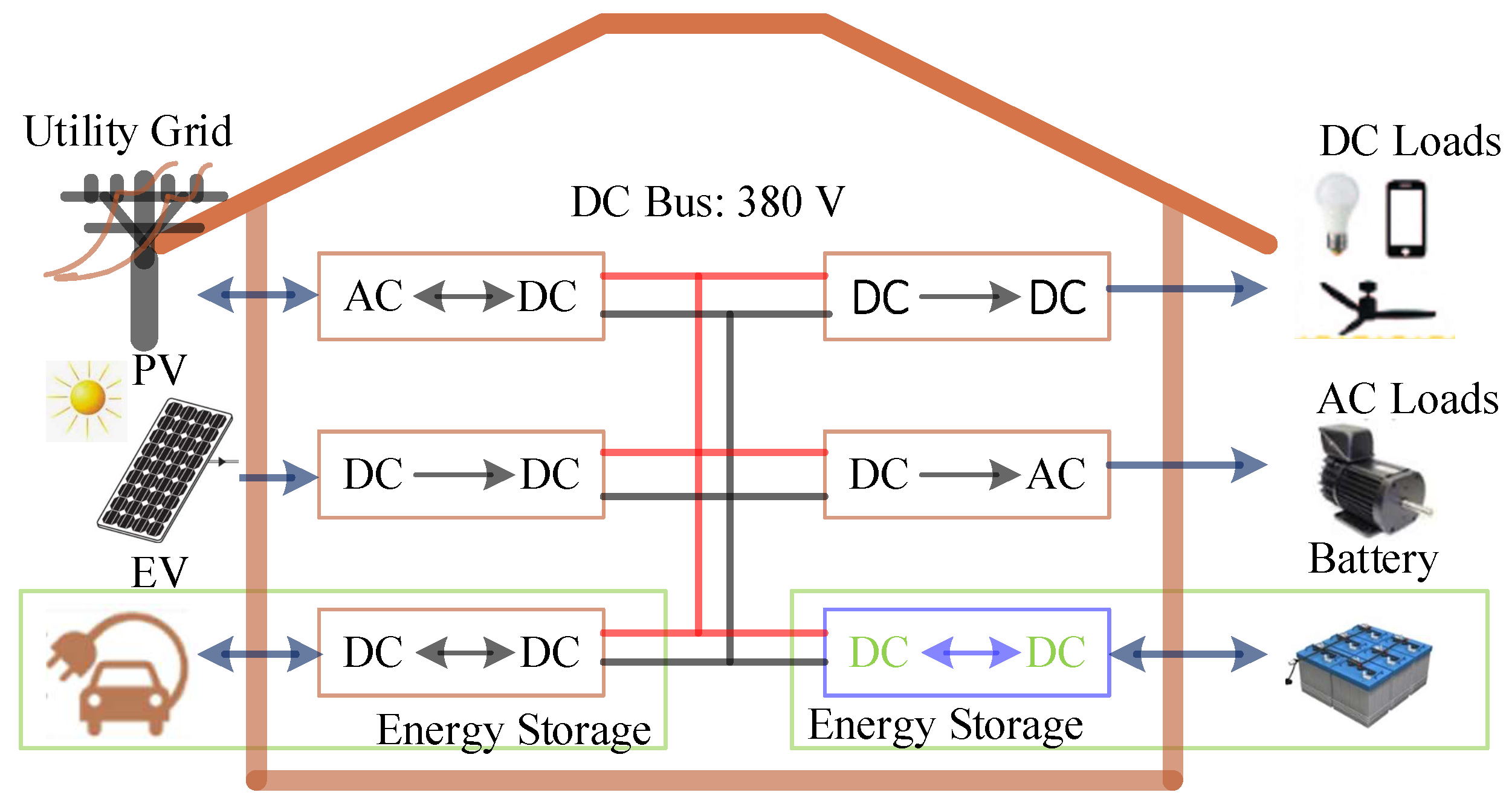
Figure 1. Block diagram of a DC microgrid system.
Energies 16 06877 g001
Figure 2. Proposed buck-type DC–DC Converter.
Energies 16 06877 g002
Figure 3. AC equivalent circuit of the LLC resonant converter based on the FHA.
Energies 16 06877 g003
Figure 4. An equivalent circuit obtained from Thévenin’s theorem based on a phasor diagram.
Energies 16 06877 g004
Figure 5. Synthetic phasor diagram.
Energies 16 06877 g005
Figure 6. Curves of voltage gain M versus normalized switching frequency fn under different quality factors of Q.
Energies 16 06877 g006
Figure 7. Curves of voltage gain M versus normalized switching frequency fn under different values of λ.
Energies 16 06877 g007
Figure 8. Illustrated waveforms at fs = fr1.
Energies 16 06877 g008
Figure 9. Case 1 current flow: (a) Mode 1; (b) Mode 2; (c) Mode 3.
Energies 16 06877 g009
Figure 10. Illustrated waveforms at fs > fr1.
Energies 16 06877 g010
Figure 11. Case 2 current flow: (a) Mode 1; (b) Mode 2; (c) Mode 3; (d) Mode 4.
Energies 16 06877 g011
Figure 12. Illustrated waveforms at fs < fr1.
Energies 16 06877 g012
Figure 13. Case 3 current flow: (a) Mode 1; (b) Mode 2; (c) Mode 3; (d) Mode 4.
Energies 16 06877 g013
Figure 14. Proposed step-up DC–DC Converter.
Energies 16 06877 g014
Figure 15. Equivalent circuit based on phasor diagram.
Energies 16 06877 g015
Figure 16. Relationship between the voltage input–output ratio and normalized frequency of the series resonant circuit.
Energies 16 06877 g016
Figure 17. Illustrated waveforms.
Energies 16 06877 g017
Figure 18. Current flow: (a) Mode 1; (b) Mode 2; (c) Mode 3; (d) Mode 4; (e) Mode 5: (f) Mode 6.
Energies 16 06877 g018
Figure 19. System configuration for the bidirectional LLC full-bridge resonant converter charge/discharge.
Energies 16 06877 g019
Figure 20. Block diagram of the main program.
Energies 16 06877 g020
Figure 21. Flowchart of battery charging.
Energies 16 06877 g021
Figure 22. Flowchart of forward-mode DSP control ISR.
Energies 16 06877 g022
Figure 23. Flowchart of battery discharge.
Energies 16 06877 g023
Figure 24. Flowchart of backward-mode DSP control ISR.
Energies 16 06877 g024
Figure 25. Instrumentation configuration for the experimental setup.
Energies 16 06877 g025
Figure 26. Proposed main power stage on the top side and its peripheral circuits.
Energies 16 06877 g026
Figure 27. Proposed main power stage on the bottom side and its peripheral circuits.
Energies 16 06877 g027
Figure 28. Forward charging mode: charging voltage (black) and charging current (blue).
Energies 16 06877 g028
Figure 29. Forward charging mode under output voltage of 44 V and current of 5 A: vgs1 and vgs4 (yellow); vgs2 and vgs3 (green); iLr (red); v2 (blue).
Energies 16 06877 g029
Figure 30. Forward power flow under output voltage of 48 V and current of 9.5 A: vgs1 and vgs4 (yellow); vgs2 and vgs3 (green); iLr (red); v2 (blue).
Energies 16 06877 g030
Figure 31. Efficiency for forward power flow: CC mode (red); CV mode (blue).
Energies 16 06877 g031
Figure 32. Backward power flow: discharging voltage (black); discharging current (blue).
Energies 16 06877 g032
Figure 33. Backward power flow: under low-side source voltage of 51 V and current of 9.5 A: vgs5 (yellow); vds5 (green); is5 and is6 (red); v1 (blue).
Energies 16 06877 g033
Figure 34. Backward power flow under input voltage 44.5 V and current 4 A: vgs5 (yellow) and vds5 (green); is5 and is6 (red); v1 (blue).
Energies 16 06877 g034
Figure 35. Efficiency for backward power flow: CC mode (red).
Energies 16 06877 g035
Table 1. Comparison of the existing converters.
Ref. No.[12][15][17][20][25]
Parameter
Input voltage12 V70–110 V280–403 V400 V30–50 V
Output voltage400 V60 V400 V200–450 V350 V
Output power300 W300 W1 kW1 kW3 kW
Max. efficiency<90%<96%94.6%93.5%95.6%
TopologyPSFBDABCLLCCLLCL-LLC
Control techniquePhase controlPhase
control
PFMPFMPFM
No. of main switches688108
No. of inductors/
transformers/
capacitors
2/1/01/1/02/1/22/1/22/1/1
Table 2. System specifications and component specifications.
ParameterSymbolSpecification
Low-side voltageVL43~52 V
High-side voltageVH360~410 V
Output powerPo100~500 W
Resonant frequencyfr125 kHz
PFM switching frequencyFllc_s96~160 kHz
PWM switching frequencyFpp_s125 kHz
Duty cycle D0.36~0.46
Transformer turns ratioNp1:Np2:Ns4:4:36
Magnetizing inductanceLms586 µH
Leakage inductanceLlk (Lr)114 µH
Resonant capacitanceCr14.1 nF
Transformer coreT1PC40 (LP2930)
Primary-side switchesS1, S2, S3, S4IPP60R120P7
Secondary-side switchesS5, S6IPP200N15N3G
DSP microcontrollerDSPdsPIC33EP16GS502
Disclaimer/Publisher’s Note: The statements, opinions and data contained in all publications are solely those of the individual author(s) and contributor(s) and not of MDPI and/or the editor(s). MDPI and/or the editor(s) disclaim responsibility for any injury to people or property resulting from any ideas, methods, instructions or products referred to in the content.