
Influence of Water Ingress on Surface Discharges Occurring on the Silicone Gel Encapsulated Printed Circuit Boards Developed for Deep-Sea Applications

 ,
,  ,
,
Abstract
:1. Introduction
2. Literature and Motivation
2.1. Partial Discharges in Liquid and Gel Materials
2.2. Dielectric Breakdown on PCB
2.3. Reasons for a Failure and Material Degradation
2.4. Impact of Water Ingress of Moisture on PCB
3. Materials and Methods
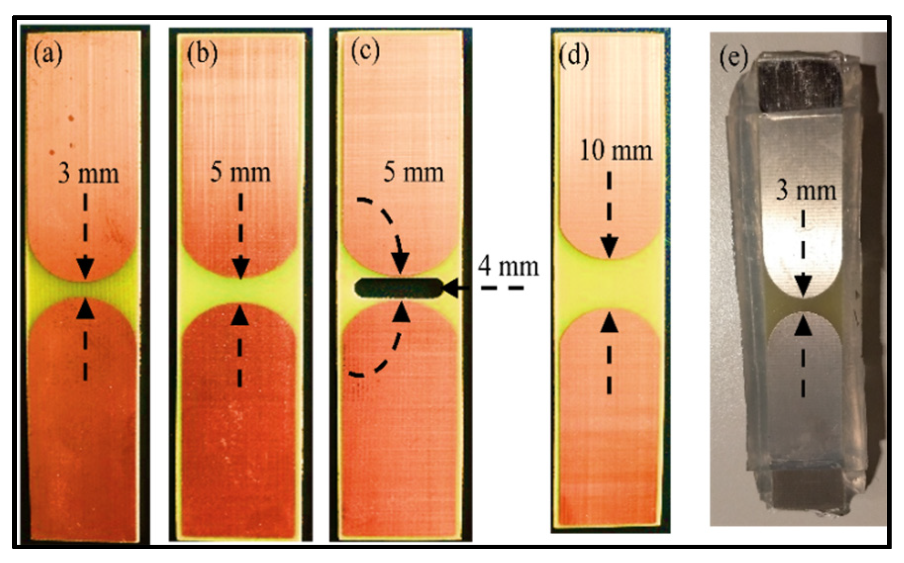
3.1. Test Samples
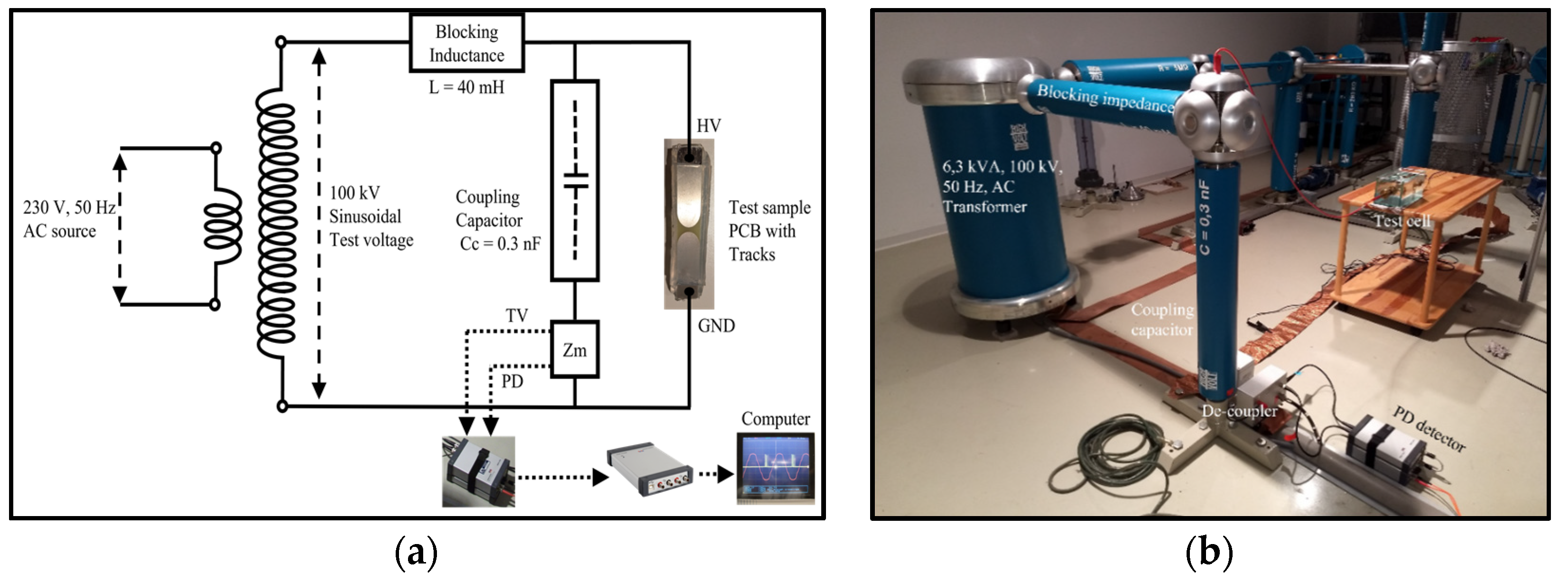
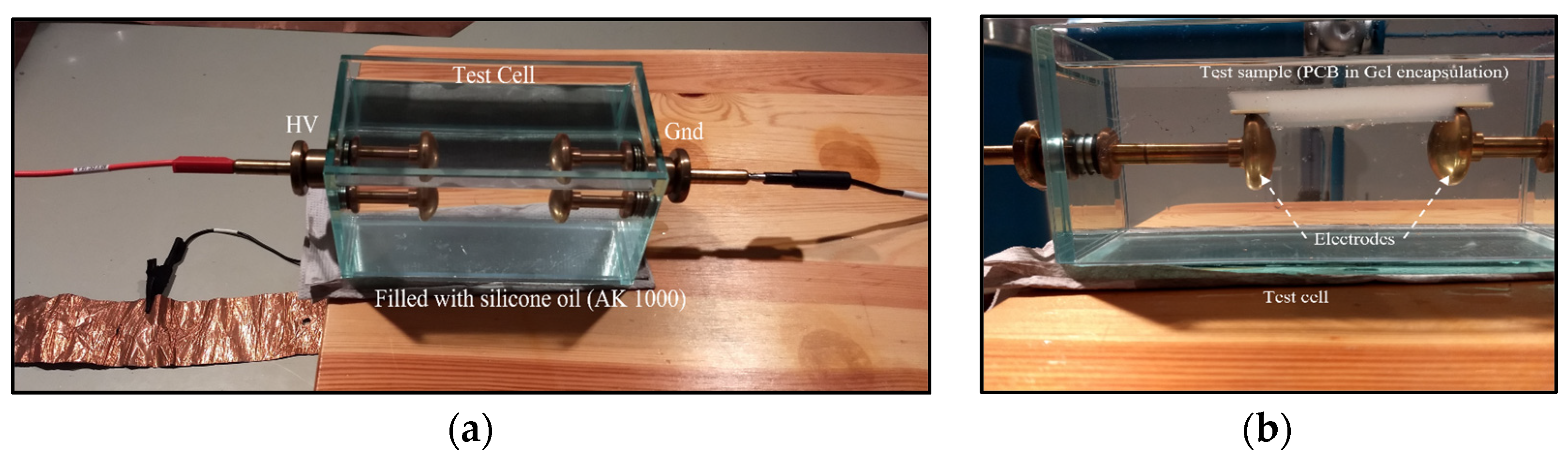
3.2. Test Setup and Test Cell
4. Results
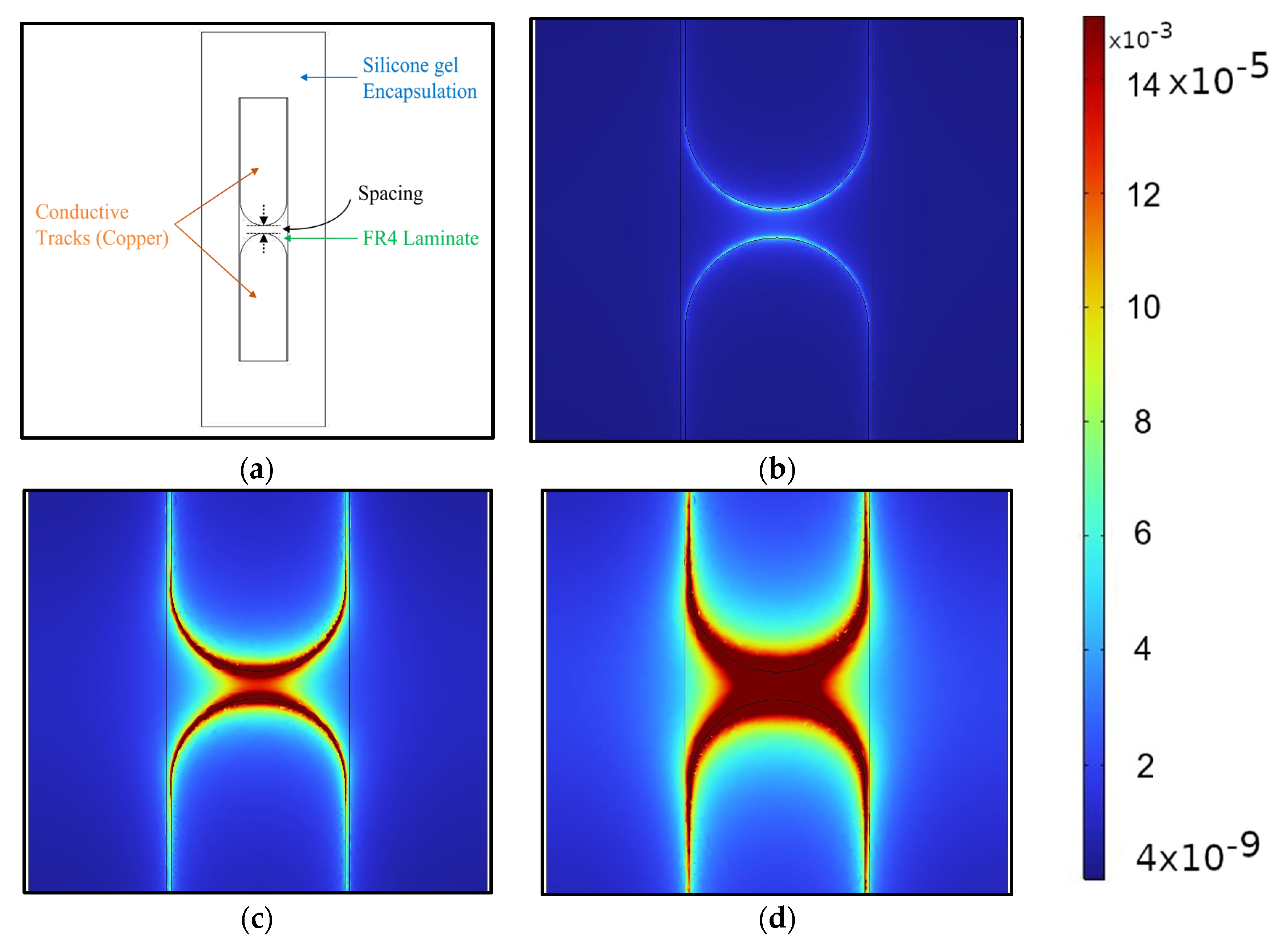
4.1. Simulation
4.2. PD Measurements
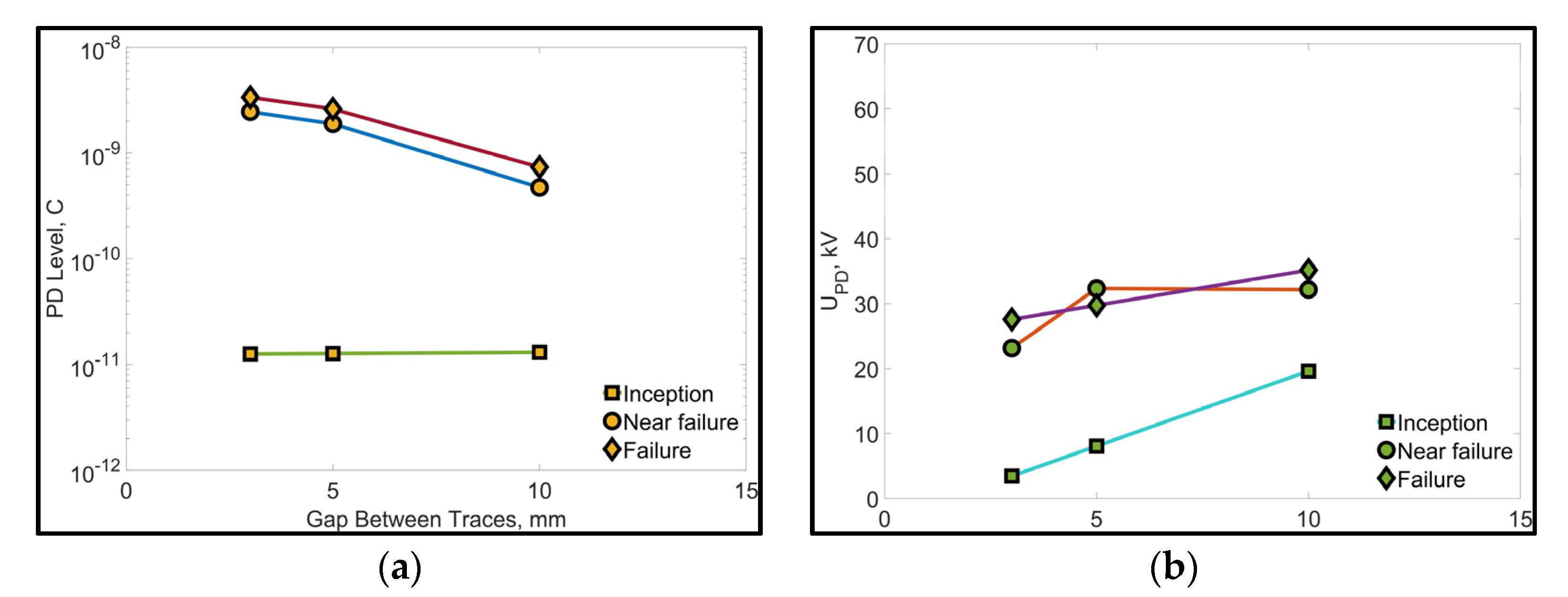
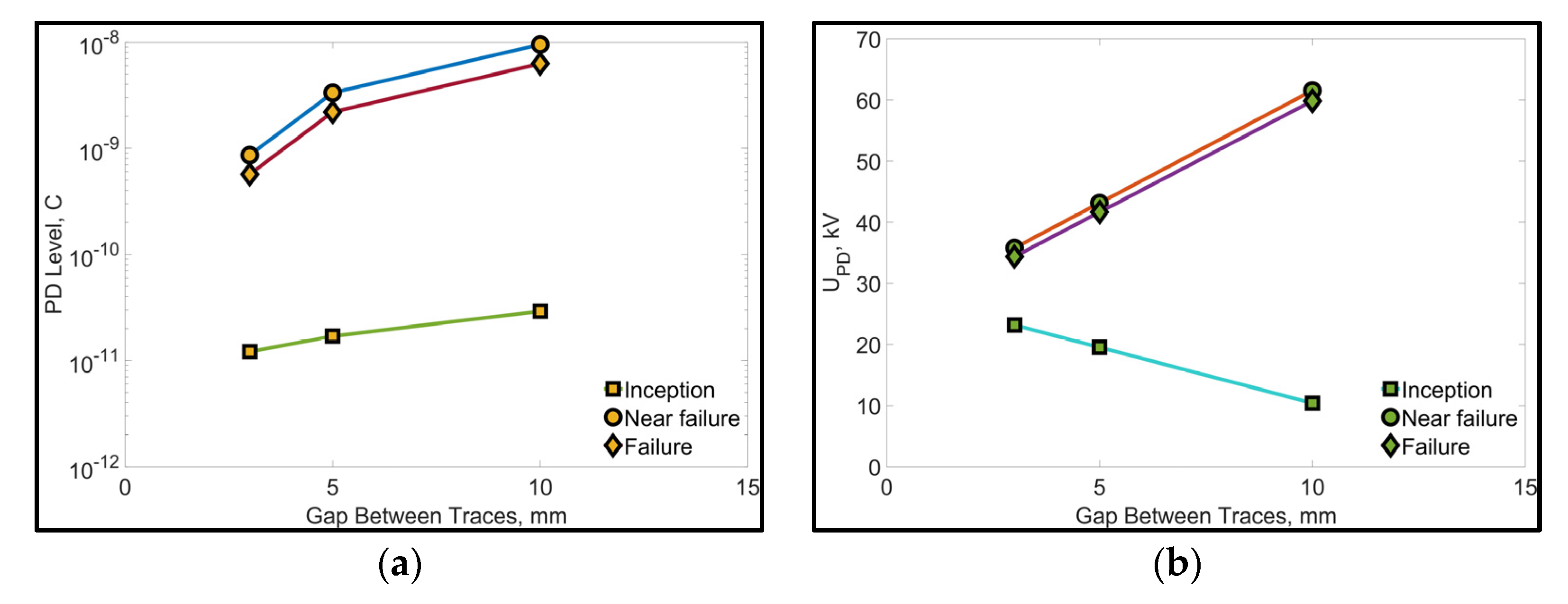
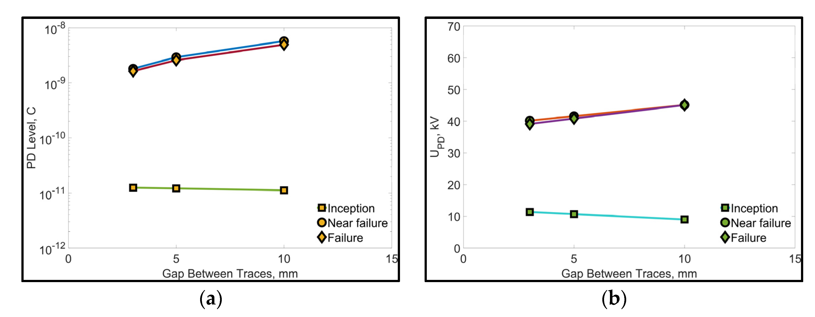
4.2.1. Influence of Spacing and Geometry
4.2.2. Influence of Deionized Water on PD Phenomena
4.2.3. Influence of Sea Water Ingress on PD Phenomena
4.3. Trend of PD Phenomenon
5. Discussion
- Simulation of a two-dimensional CAD model indicates that the electric displacement field appears predominantly at the curvature of the conductive tracks, with higher intensity at their tips. A further increase in test voltage drastically increases the intensity of the electric displacement field, not only at the curvature but also on the sides of the conductive tracks. The perpendicular displacement field increased from 192 pC (at 5 kV) to 1.15 nC (at 30 kV), respectively. It may be deduced that weaker insulation at the sides may cause a failure at these locations rather than at the semicircular ends.
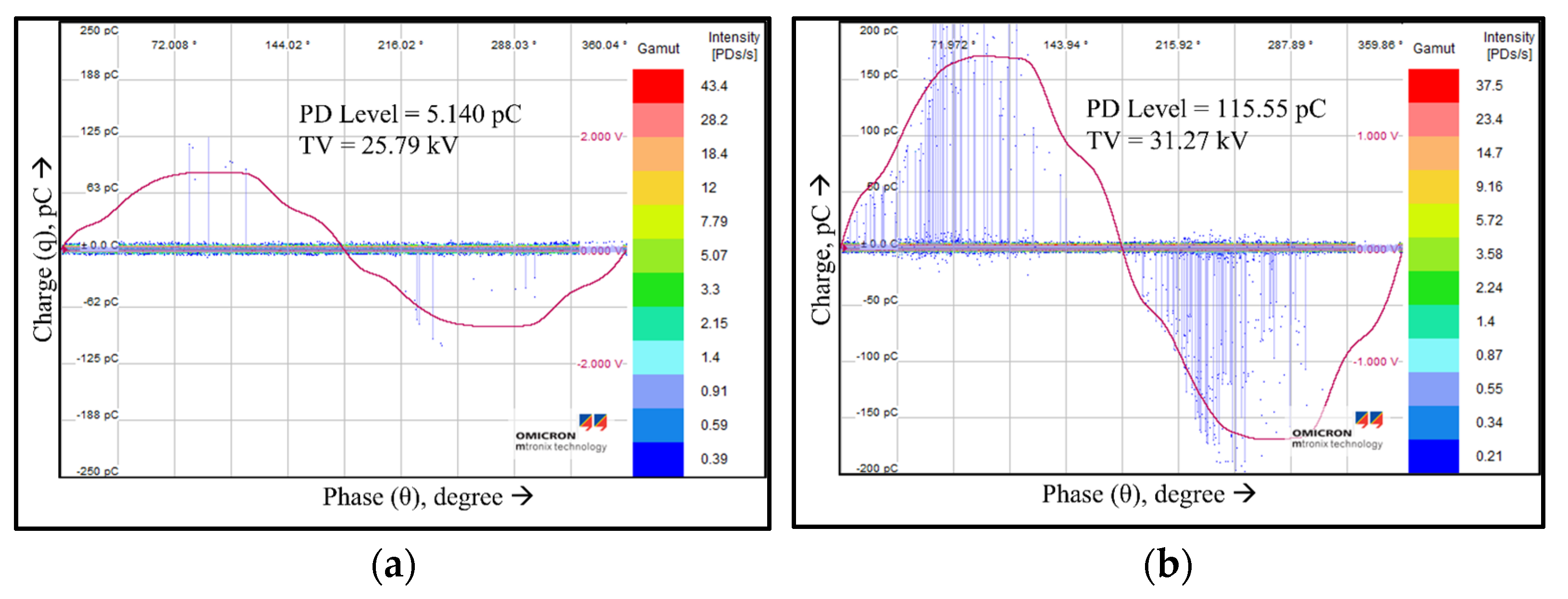
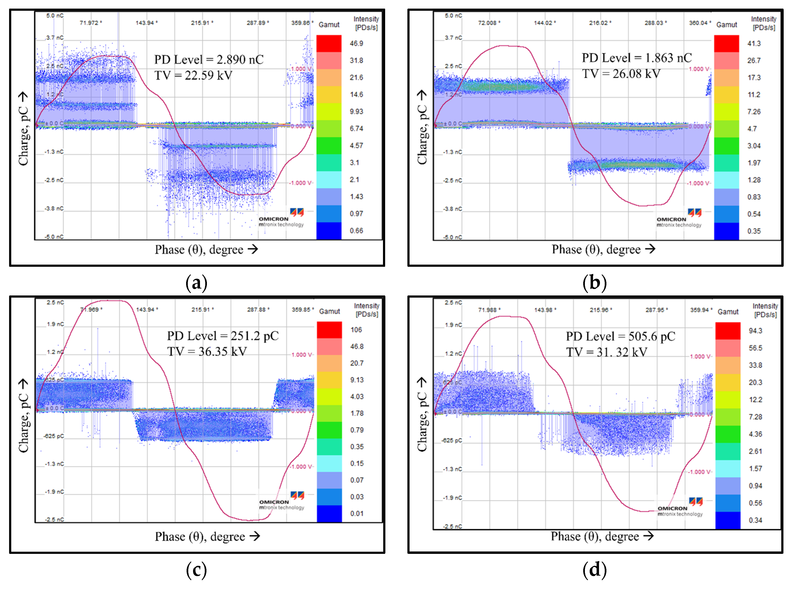
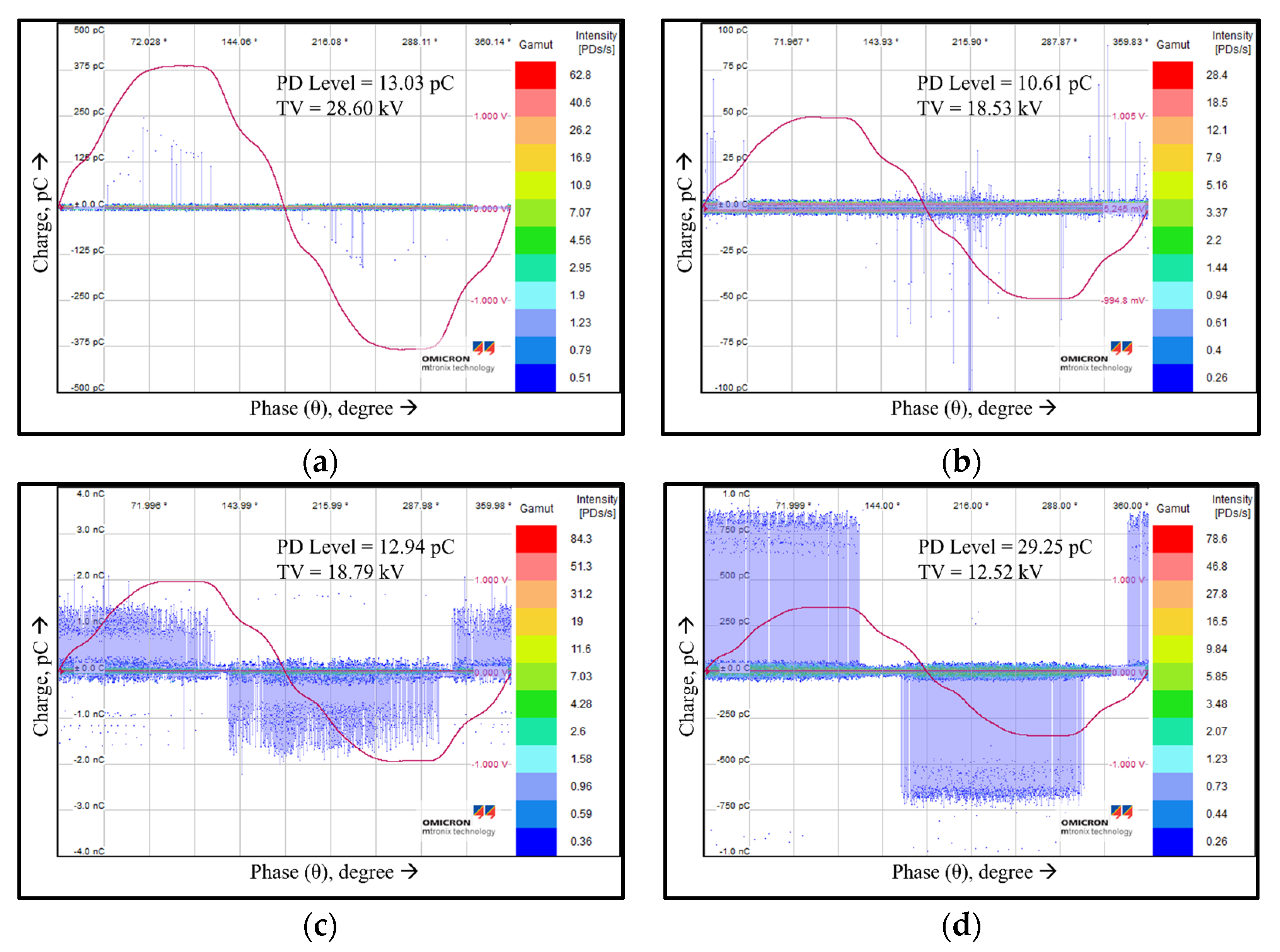
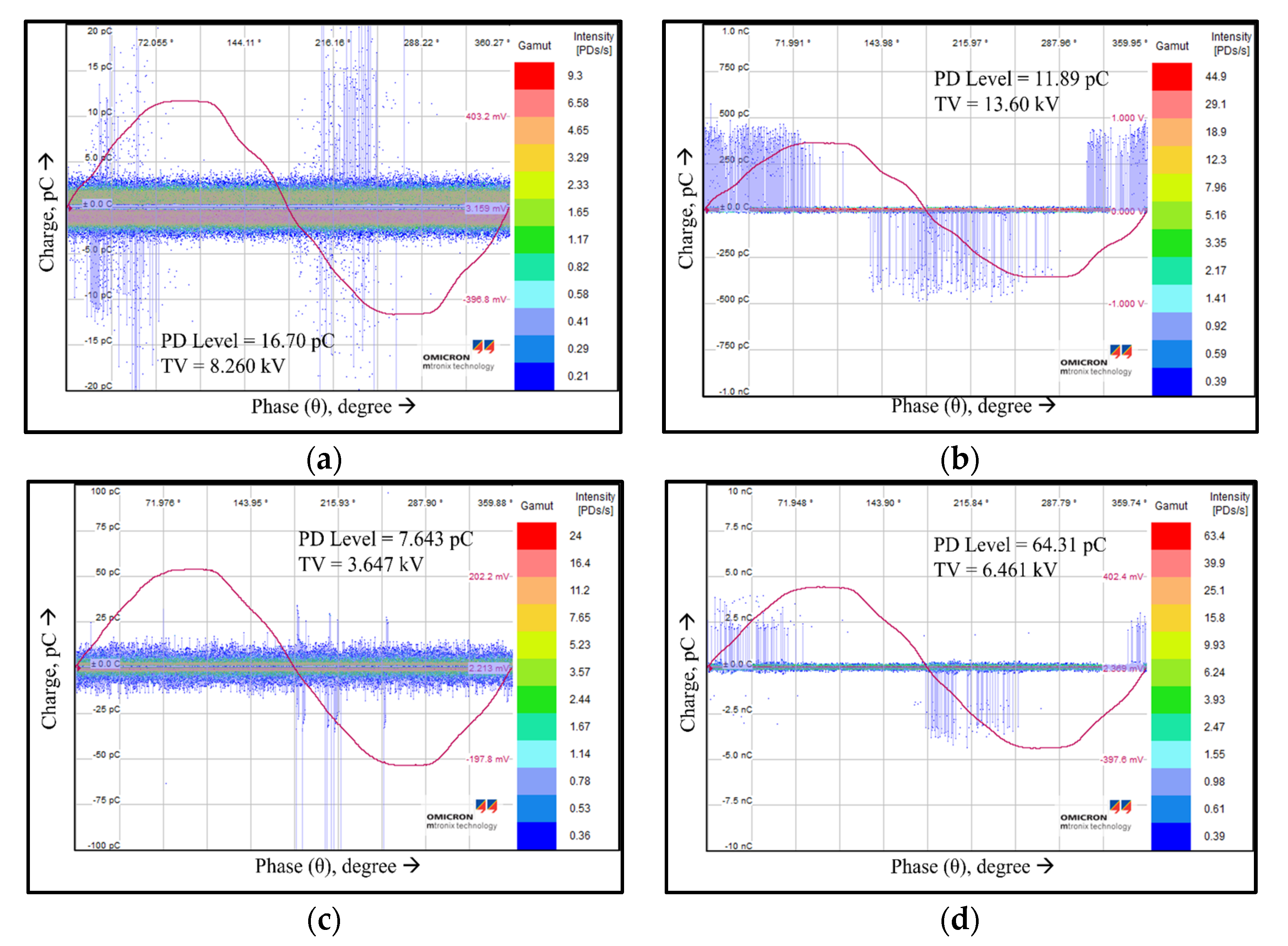
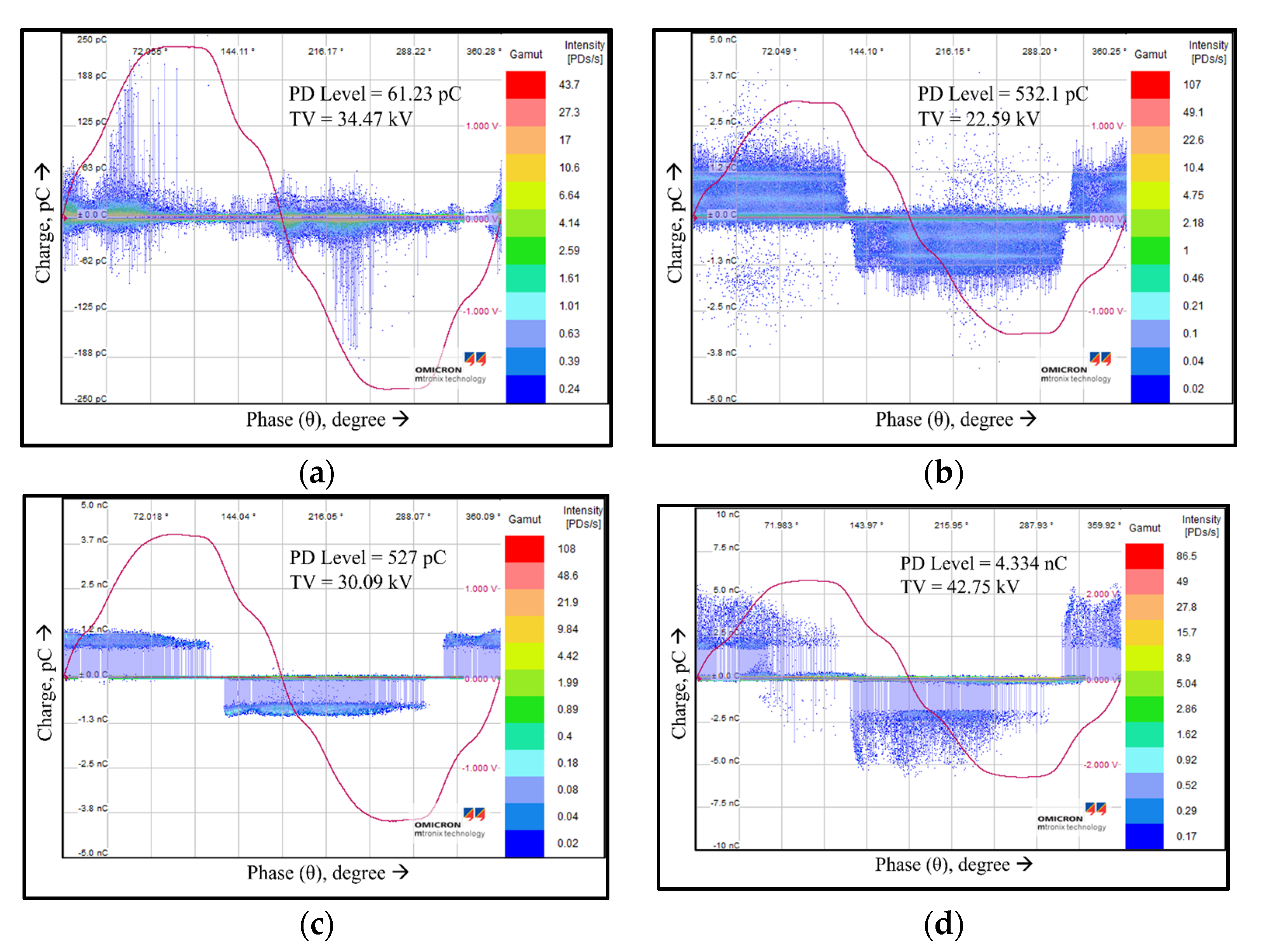
- The experiments on virgin PCB samples with and without gel encapsulation (Groups 1, 2) provide the reference values so that a comparison can be made to analyze the status of the other PCB samples aged in deionized and seawater. The PD measurements on the virgin PCB sample (Group 1) show the pattern of surface discharges directly appearing on the FR4 laminate, while the same on Group 2 shows the impact of encapsulating material on the surface discharges. Subsequent experiments revealed that the PRPD pattern of discharge events occurring on the surface of the virgin samples without gel encapsulation is similar to that of the corona. Pertinent discharge events appear as individual, strong, stable pulses that are predominantly correlated to the peaks of the applied voltage and later span into the first and third quadrants in discrete steps. As the voltage increases, so do the PD magnitude and intensity in the respective patterns. On the contrary, the discharge events occurring on the gel-encapsulated virgin sample start to appear directly in the first and third quadrants. As the applied voltage is increased, the pertinent sample reaches a near-failure condition where the discharges start to appear bipolar, predominantly negative to the applied voltage. The pulses appearing at a polarity opposite to the applied voltage indicate degradation of the gel in that location. This might be since the surface resistivity of the FR4 laminate (Ω-cm) is much lower than that of the silicone gel encapsulation ( Ω-cm). In addition to this, a certain degree of discharge pulses that are proximally positioned to each other appears but at a smaller intensity. This pattern is similar to that of brush discharges that usually arise due to curved electrode surfaces and micro-voids on the surface.
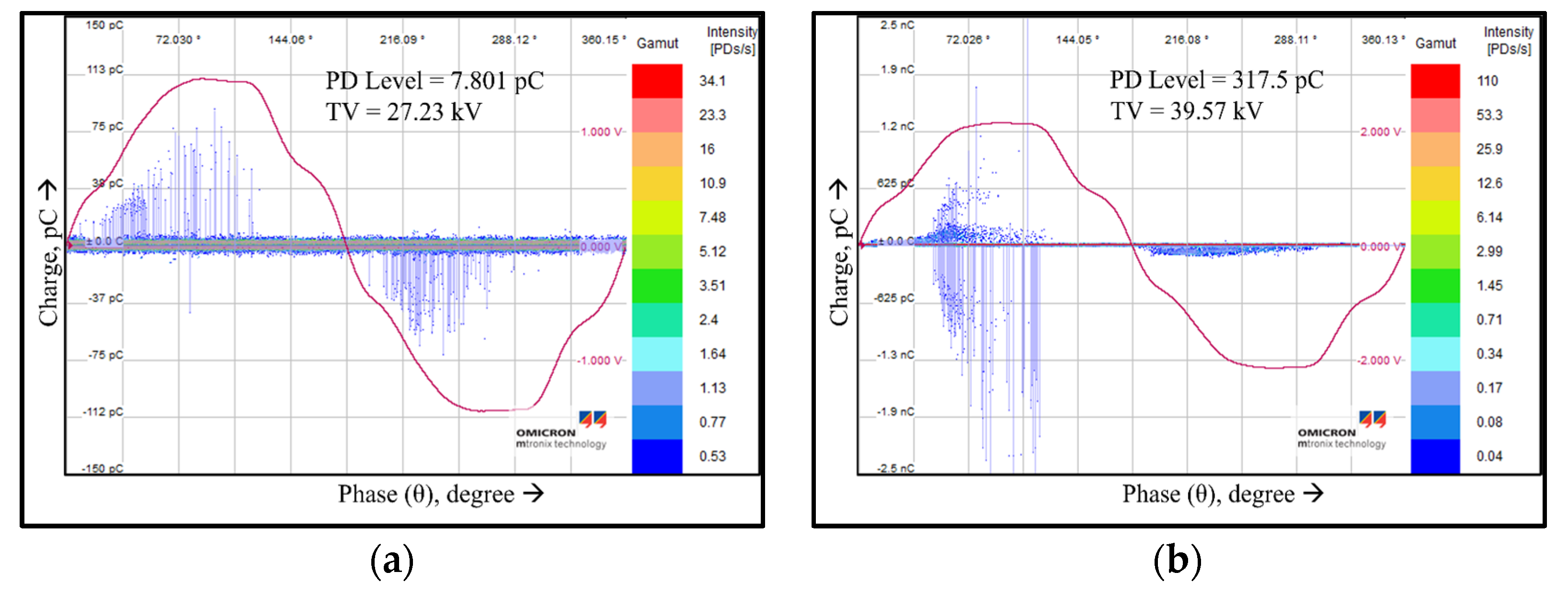
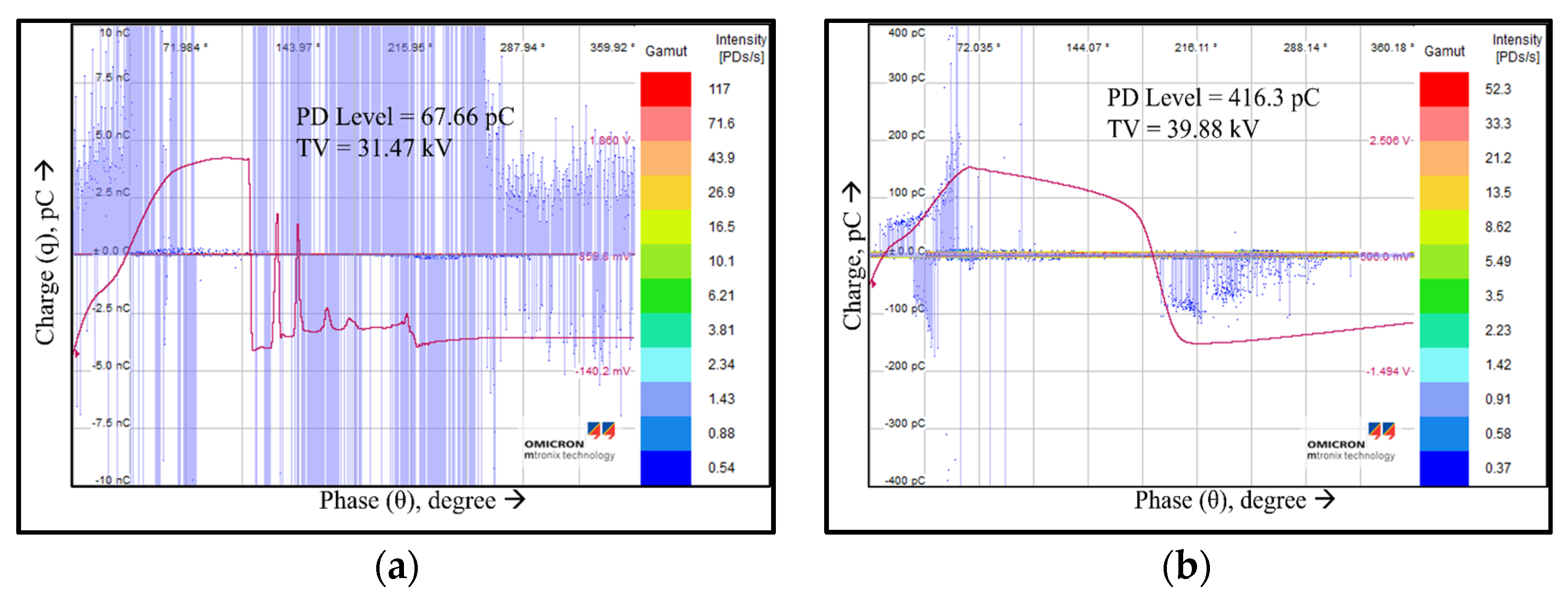
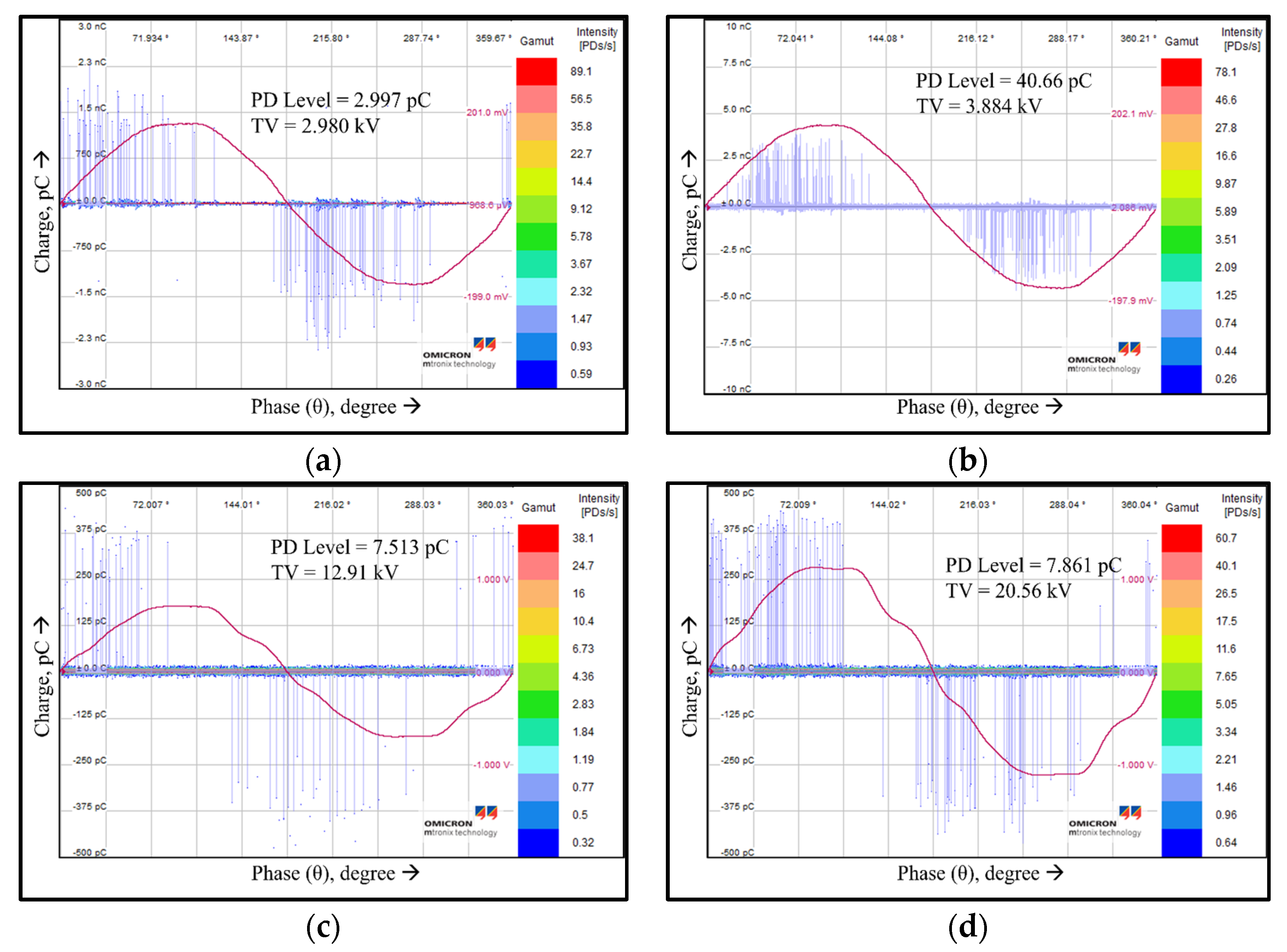
- Further experiments on gel-encapsulated PCB samples aged in deionized and seawater indicate a similar pattern but with a slight deviation in their correlation. For instance, the pattern formed by the PCB samples aged in deionized water at 90 °C seems to be more uniform. As soon as the applied voltage reaches a sufficient magnitude to initiate surface discharges, the pulses appear in the first and third quadrants with well-defined intensity levels. This behavior remains the same for all the samples with different gaps. The only difference is the intensity of PD measured and the magnitude of applied voltage. As the magnitude of applied voltage increases, the intensity of discharges increases, causing severe events that eventually cause a permanent failure. Pertinent patterns appear similar to those of brush discharges, and henceforth the location suffers degradation. On the contrary, similarities between deionized and seawater-aged samples at room temperature were observed, especially for PCB samples with a 3 mm track spacing. A prominent PRPD pattern indicated that the surface discharges are initiated by the field enhancements at the curved electrodes. At the same time, the QV diagram pointed out that the sample with 3 mm track spacing had several opportunities for momentary discharges. As the voltage is higher, the intensity of such discharges is higher, eventually resulting in brush-type discharge failure. Since the brush-type discharges have more energy than their corona counterparts, there is always a likely chance that the gel encapsulation might suffer degradation. In addition, it was observed that the PCB sample with 5 mm track spacing and an additional slit between the conductive tracks showed better PD characteristics. The operating voltage can be increased, while the apparent charge responsible for PD failure is also lower. So, the material degradation can be less than for the other geometries. In addition, the sample with 10 mm spacing also emerges with better characteristics but may not be a feasible choice where high-power density is considered.
6. Conclusions
Author Contributions
Funding
Data Availability Statement
Acknowledgments
Conflicts of Interest
References
- Gray, E.; Harrington, D. Surface Topography of Printed Wiring Boards and Its Effect on Flashover. IEEE Trans. Compon. Hybrids Manuf. Technol. 1982, 5, 142–146. [Google Scholar] [CrossRef]
- Du, B.X.; Liu, Y.; Liu, H.J. Effects of low pressure on tracking failure of printed circuit boards. IEEE Trans. Dielectr. Electr. Insul. 2008, 15, 1379–1384. [Google Scholar] [CrossRef]
- Fulnecek, J.; Kabot, O.; Prokop, L. High Voltage PCBs in Low Pressure and High Temperature Environment. In Proceedings of the 2021 Selected Issues of Electrical Engineering and Electronics (WZEE), Rzeszow, Poland, 13–15 September 2021; pp. 1–4. [Google Scholar] [CrossRef]
- Pieterse, P.J.; Bekker, M.; Arumugam, S.; Uhrlandt, D. Breakdown of Water Saturated Printed Circuit Boards in Dielectric Encapsulation for Deep-Sea Applications. In Proceedings of the 2022 IEEE Conference on Electrical Insulation and Dielectric Phenomena (CEIDP), East Rutherford, NJ, USA, 15–19 October 2022; pp. 393–396. [Google Scholar] [CrossRef]
- Arumugam, S.; Gorchakov, S.; Schoenemann, T. Dielectric and partial discharge investigations on high power insulated gate bipolar transistor modules. IEEE Trans. Dielectr. Electr. Insul. 2015, 22, 1997–2007. [Google Scholar] [CrossRef]
- Barnes, H.E.; Gennari, J.J. A Review of Pressure-Tolerant Electronics (PTE); Final Report Naval Research Lab.: Washington, DC, USA, 1976. [CrossRef]
- Gao, Y.; Wang, J.; Liang, X.; Yan, Z.; Liu, Y.; Cai, Y. Investigation on permeation properties of liquids into HTV silicone rubber materials. IEEE Trans. Dielectr. Electr. Insul. 2014, 21, 2428–2437. [Google Scholar] [CrossRef]
- Pieterse, P.; Hilbert, M.; Gortschakow, S.; Uhrlandt, D. The Effect of Water Saturation on Silicone Rubber Surface Discharge Behaviour. In Proceedings of the 21st International Symposium on High Voltage Engineering, Budapest, Hungary, 26–30 August 2019; pp. 592–601. [Google Scholar] [CrossRef]
- Arumugam, S.; Krohmann, S.; Haba, Y.; Pieterse, P.J.; Uhrlandt, D.; Kosleck, S. Electrical Studies to Understand the Water Absorption Behaviour of Polyoxymethylene used for Deep Sea Applications. In Proceedings of the 2021 IEEE Electrical Insulation Conference (EIC), Denver, CO, USA, 7–28 June 2021; pp. 651–655. [Google Scholar] [CrossRef]
- Plessow, R.; Pfeiffer, W. Influence of the frequency on the partial discharge inception voltage. In Proceedings of the IEEE Conference on Electrical Insulation and Dielectric Phenomena-(CEIDP’94), Arlington, TX, USA, 23–26 October 1994. [Google Scholar] [CrossRef]
- Vampola, A. The nature of bulk charging and its mitigation in spacecraft design. In Proceedings of the Wescon/96, Anaheim, CA, USA, 22–24 October 1996; pp. 268–273. [Google Scholar] [CrossRef]
- Maeda, T.; Haga, K.; Maeda, T. Creepage breakdown characteristics of printed wiring board in silicone gel. In Proceedings of the 1995 International Symposium on Electrical Insulating Materials, Tokyo, Japan, 17–20 September 1995. [Google Scholar] [CrossRef]
- Maeda, T.; Haga, K.; Maeda, T. Creepage breakdown characteristics of printed wiring board in silicone gel. In Proceedings of the Conference on Electrical Insulation and Dielectric Phenomena-CEIDP ’96, Millbrae, CA, USA, 23 October 1996. [Google Scholar] [CrossRef]
- Du, B.; Xiao, J.; Zhang, X. Dielectric breakdown and discharge energy on printed circuit board. In Proceedings of the 2004 IEEE International Conference on Solid Dielectrics, 2004. ICSD 2004, Toulouse, France, 5–9 July 2004. [Google Scholar] [CrossRef]
- Du, B.; Gao, Y. Dielectric breakdown of printed circuit board under magnetic field. In Proceedings of the 2005 International Symposium on Electrical Insulating Materials, 2005. (ISEIM 2005), Kitakyushu, Japan, 5–9 June 2005; Volume 2, pp. 308–311. [Google Scholar] [CrossRef]
- Du, B. Surface breakdown of printed circuit board under dc magnetic field. In Proceedings of the 2003 Annual Report Conference on Electrical Insulation and Dielectric Phenomena, Albuquerque, NM, USA, 19–22 October 2003. [Google Scholar] [CrossRef]
- Hu, C.; Zhou, L. Failure analysis for micro-short circuit between two pins in printed circuit board assembly. In Proceedings of the 2016 11th International Conference on Reliability, Maintainability and Safety (ICRMS), Hangzhou, China, 26–28 October 2016; pp. 1–4. [Google Scholar] [CrossRef]
- Lin, Z.; Zhou, Y.; Chen, Z. Failure analysis and case study of board burning. In Proceedings of the 2020 21st International Conference on Electronic Packaging Technology (ICEPT), Guangzhou, China, 12–15 August 2020; pp. 1–3. [Google Scholar] [CrossRef]
- Emersic, C.; Lowndes, R.; Cotton, I.; Rowland, S.; Freer, R. Observations of breakdown through printed circuit board polymer coatings via a surface pollution layer. IEEE Trans. Dielectr. Electr. Insul. 2017, 24, 2570–2578. [Google Scholar] [CrossRef]
- Guastavino, F.; Centurioni, L.; Coletti, G.; Ratto, A.; Torello, E. Electrical characterization of multi-layered printed circuit boards. In Proceedings of the The 17th Annual Meeting of the IEEE Lasers and Electro-Optics Society, 2004. LEOS 2004, Boulder, CO, USA, 20 October 2004. [Google Scholar] [CrossRef]
- Kasten, D.; Chen, T.; Rockwell, M.; Sebo, S.; Grosjean, D.; Schweickart, D. Flashover and breakdown investigations of aircraft wiring in low pressure environment. In Proceedings of the 2010 IEEE International Power Modulator and High Voltage Conference, Atlanta, GA, USA, 23–27 May 2010; pp. 501–504. [Google Scholar] [CrossRef]
- Lincoln, J.D.; Shapiro, A.; Saphores, J.-D.M.; Ogunseitan, O.A. Moisture absorption phenomena in green composite printed circuit board prototypes. In Proceedings of the 2008 IEEE International Symposium on Electronics and the Environment, San Francisco, CA, USA, 19–22 May 2008; pp. 1–6. [Google Scholar] [CrossRef]
- Arumugam, S.; Haba, Y.; Koerner, G.; Uhrlandt, D.; Paschen, M. Understanding partial discharges in low-power relay and silicone cable modified to suit high-voltage requirement of deep sea electrical system. Int. Trans. Electr. Energy Syst. 2018, 28, e2542. [Google Scholar] [CrossRef]
- Arumugam, S. Influence of moisture on dielectric condition of high power Insulated Gate Bipolar Transistor modules. IEEE Trans. Dielectr. Electr. Insul. 2016, 23, 1364–1374. [Google Scholar] [CrossRef]
- Abdelmalik, A.A.; Nysveen, A.; Lundgaard, L.E. Partial discharges in liquid embedded power electronics: Effects of pressure and liquid nature under negative pulse voltage stress. IEEE Trans. Dielectr. Electr. Insul. 2016, 23, 1119–1125. [Google Scholar] [CrossRef]
- Abdelmalik, A.; Nysveen, A.; Lundgaard, L. Partial discharges in narrow gaps on power electronic converter. In Proceedings of the 2014 IEEE Conference on Electrical Insulation and Dielectric Phenomena (CEIDP), Des Moines, IA, USA, 19–22 October 2014; pp. 31–34. [Google Scholar] [CrossRef]
- Zecha, H.; Fruh, C.; Ratchev, R.; Biehl, E.; Zerna, T. Absorption and diffusion of water in printed circuit boards. In Proceedings of the 36th International Spring Seminar on Electronics Technology, Alba Iulia, Romania, 8–12 May 2013; pp. 121–126. [Google Scholar] [CrossRef]
- Xie, C.; Tang, X.; Song, B.; Jin, J. Study on the Effect of Moisture Stress on Printed Circuit Board of Numerical Control System. In Proceedings of the 2012 Second International Conference on Instrumentation, Measurement, Computer, Communication and Control, Harbin, China, 8–10 December 2012; pp. 1661–1665. [Google Scholar] [CrossRef]
- Khoshnaw, F.M. Evaluation the moisture effects on the performance of electronic devices. In Proceedings of the 2010 IEEE 14th Workshop on Signal Propagation on Interconnects, Hildesheim, Germany, 9–12 May 2010; pp. 59–61. [Google Scholar] [CrossRef]
- Lahokallio, S.; Saarinen, K.; Frisk, L. Changes in water absorption and modulus of elasticity of flexible printed circuit board materials in high humidity testing. In Proceedings of the 18th European Microelectronics & Packaging Conference, Brighton, UK, 12–15 September 2011; pp. 1–6. [Google Scholar]
- DIN 50905-4:2018-03; Korrosion der Metalle-Korrosionsuntersuchungen-Teil 4: Durchführung von Chemischen Korrosionsversuchen ohne Mechanische Belastung in Flüssigkeiten im Laboratorium. Beuth Publishing DIN, 2018. Available online: https://www.beuth.de/en/standard/din-50905-4/282022110 (accessed on 9 July 2023). [CrossRef]


| Group | Test Samples | Gap between Tracks | Test Conditions |
|---|---|---|---|
| 1 | Virgin PCB 1 | 5 mm | Without gel encapsulation |
| 2 | Virgin PCB 2 | 5 mm | With gel encapsulation |
| 3 | 3 mm | ||
| PCB 3 | 5 mm | Deionized water at 90 °C | |
| 5 mm with 4 mm slit | |||
| 10 mm | |||
| 4 | 3 mm | ||
| PCB 3 | 5 mm | Deionized water at | |
| 5 mm with 4 mm slit | room temperature (RT) | ||
| 10 mm | |||
| 5 | 3 mm | ||
| PCB 3 | 5 mm | Sea water in room | |
| 5 mm with 4 mm slit | temperature | ||
| 10 mm |
| Spacing between the Tracks | |||
|---|---|---|---|
| Maximum Value Simulated at 5 kV | Maximum Value Simulated at 30 kV | Maximum Value Simulated at 60 kV | |
| C/mm2 | C/mm2 | C/mm2 | |
| 3 mm | 192 | 1.15 | 2.3 |
| 5 mm | 151 | 908 | 1.89 |
| 10 mm | 110 | 662 | 1.32 |
| Test Condition | Spacing | Discharge Inception | Nearing Failure | Failure Due to Discharge | |||
|---|---|---|---|---|---|---|---|
| App. Charge | Voltage | App. Charge | Voltage | App. Charge | Voltage | ||
| mm | C | kV | C | kV | C | kV | |
| 1 Air | 5 | 26.94 | 31.95 | 32.23 | |||
| 2 Sil. oil | 5 | 27.41 | 40.6 | 40.61 | |||
| Spacing | Discharge Inception | Nearing Failure | Failure Due to Discharge | |||
|---|---|---|---|---|---|---|
| App. Charge | Voltage | App. Charge | Voltage | App. Charge | Voltage | |
| mm | C | kV | C | kV | C | kV |
| 3 | 3.128 | 23.15 | 23.36 | |||
| 5 | 3.579 | 26.54 | 26.89 | |||
| 5 (Slit) | 13.03 | 38.14 | 38.51 | |||
| 10 | 19.48 | 32.16 | 33.48 | |||
| Spacing | Discharge Inception | Nearing Failure | Failure Due to Discharge | |||
|---|---|---|---|---|---|---|
| App. Charge | Voltage | App. Charge | Voltage | App. Charge | Voltage | |
| Mm | C | kV | C | kV | C | kV |
| 3 | 28.72 | 33.17 | 33.24 | |||
| 5 | 12.26 | 43.93 | 46.46 | |||
| 5 (slit) | 19.02 | 41.02 | 43.36 | |||
| 10 | 12.61 | 59.36 | 60.51 | |||
| Spacing | Discharge Inception | Nearing Failure | Failure Due to Discharge | |||
|---|---|---|---|---|---|---|
| App. Charge | Voltage | App. Charge | Voltage | App. Charge | Voltage | |
| Mm | C | kV | C | kV | C | kV |
| 3 | 4.177 | 35.38 | 36.65 | |||
| 5 | 8.565 | 38.93 | 39.16 | |||
| 5 (Slit) | 22.97 | 47.93 | 48.88 | |||
| 10 | 6.117 | 43.62 | 43.72 | |||
Disclaimer/Publisher’s Note: The statements, opinions and data contained in all publications are solely those of the individual author(s) and contributor(s) and not of MDPI and/or the editor(s). MDPI and/or the editor(s) disclaim responsibility for any injury to people or property resulting from any ideas, methods, instructions or products referred to in the content. |
© 2023 by the authors. Licensee MDPI, Basel, Switzerland. This article is an open access article distributed under the terms and conditions of the Creative Commons Attribution (CC BY) license (https://creativecommons.org/licenses/by/4.0/).
Share and Cite
Arumugam, S.; Haba, Y.; Pieterse, P.J.; Uhrlandt, D.; Kosleck, S. Influence of Water Ingress on Surface Discharges Occurring on the Silicone Gel Encapsulated Printed Circuit Boards Developed for Deep-Sea Applications. Energies 2023, 16, 5353. https://doi.org/10.3390/en16145353
Arumugam S, Haba Y, Pieterse PJ, Uhrlandt D, Kosleck S. Influence of Water Ingress on Surface Discharges Occurring on the Silicone Gel Encapsulated Printed Circuit Boards Developed for Deep-Sea Applications. Energies. 2023; 16(14):5353. https://doi.org/10.3390/en16145353
Chicago/Turabian StyleArumugam, Saravanakumar, Yvonne Haba, Petrus Jacobus Pieterse, Dirk Uhrlandt, and Sascha Kosleck. 2023. "Influence of Water Ingress on Surface Discharges Occurring on the Silicone Gel Encapsulated Printed Circuit Boards Developed for Deep-Sea Applications" Energies 16, no. 14: 5353. https://doi.org/10.3390/en16145353
APA StyleArumugam, S., Haba, Y., Pieterse, P. J., Uhrlandt, D., & Kosleck, S. (2023). Influence of Water Ingress on Surface Discharges Occurring on the Silicone Gel Encapsulated Printed Circuit Boards Developed for Deep-Sea Applications. Energies, 16(14), 5353. https://doi.org/10.3390/en16145353