1. Introduction
The generation of high-voltage pulses is needed for carrying out a variety of tests and research. These concern not only the simulation of lightning discharges [
1] or dielectric strength tests, but also the acceleration of particles [
2,
3,
4,
5], the generation of strong X-rays [
6], high-power microwaves [
7], biological applications [
8] or food processing [
9,
10]. Marx generators are very often used in such applications. This type of device has a number of advantages: a simple construction, low cost of components, simple voltage regulation and expandability.
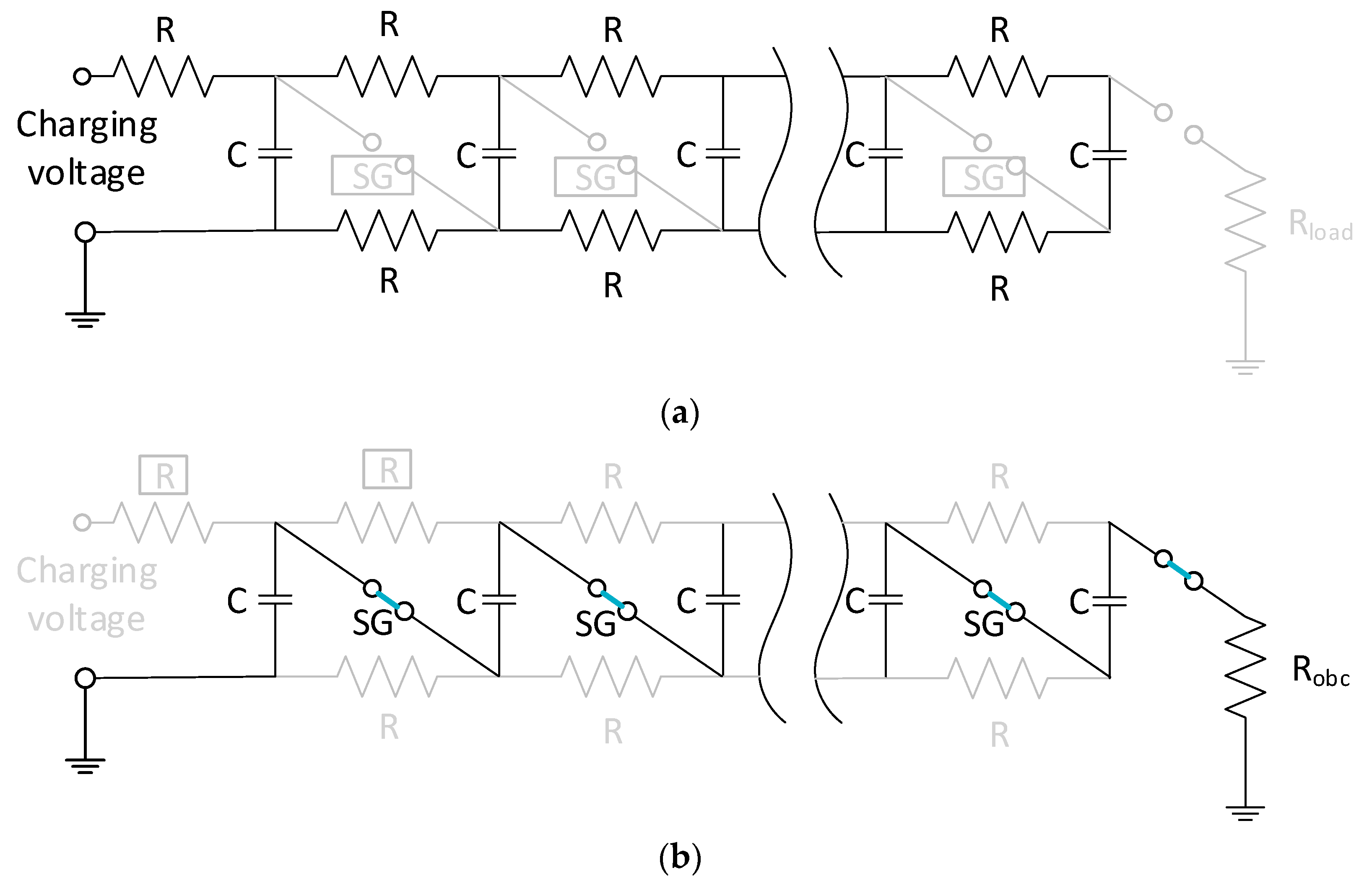
Problems may arise when it is necessary to generate many highly repetitive pulses with a high frequency, exceeding 1 pulse per second. By analyzing the construction of a conventional Marx generator (
Figure 1), it can be seen why this task is quite difficult to accomplish: the resistance of the resistors connecting the capacitors in parallel in the charging phase (
Figure 1a) must be much higher than the resistance of the spark gaps in the discharge phase (
Figure 1b). Otherwise, the efficiency of the generator will drop significantly or the device will not work at all. On the other hand, the high resistance of these resistors increases the time constant of the system during charging, which does not allow all the capacitors to be recharged in a sufficiently short time. Therefore, in such applications instead of resistors, inductors [
10] are often used, or solutions with diodes in the charging circuit and high-voltage transistors as triggers [
11].
An additional problem is the development of an appropriately efficient power supply. In order for the Marx generator to function properly, each of the stages (each of the capacitors) should be charged to a sufficiently high voltage needed to break down the spark gap. It should also be noted that a large number of stages reduces the efficiency of the device and the speed of its operation. Therefore, it is desirable that the power supply should generate the highest possible voltage. This causes a number of problems. The first is the performance of the power supply. The output current of such a device should be high enough to charge the generator capacitors to a sufficiently high voltage in an appropriately short time. In addition, the power supply should enable simple adjustment of the output voltage (preferably in a digital way), have a current limitation, compact dimensions and low weight.
For this purpose, high-frequency transformer-based converters are most commonly used. A literature review performed in the area of high-voltage power supplies for rapid capacitor charging showed that in most cases, topologies with full-bridge converters are used [
12,
13,
14,
15,
16,
17,
18,
19] due to the versatility of this topology and the possibility of implementing various control algorithms.
In [
12,
13,
14], a simple hard-switched duty cycle control method was used, but this way of control may cause significant electromagnetic disturbance and large power losses [
20]. Therefore, a method with phase-shifted modulation is much more often used [
15,
16]. In a large number of applications, a resonant converter can be found [
17,
18]. This method has several benefits. The main advantage is that switching of the transistors occurs in a deenergized state, which significantly reduces the losses and the electromagnetic disturbances caused by this process. However, the development of the resonant converters is problematic, especially when transformers with high parasitic capacitance are used.
An interesting solution was described in [
19] where a series connection of the DC-DC converters (double-boost and isolated resonant) was used.
In high-voltage power supplies, solutions involving only one transformer and a simple rectifier are not used often. To increase the voltage, popular solutions include the usage of several transformers with separated rectifiers connected in series [
14], voltage multipliers such as the Villard cascade [
17] or a combination of these solutions [
19] where SiC MOSFETs are also used.
The multitude of solutions shows that the problem of building high-voltage power supplies, in particular for rapid charging of Marx generators, is not a trivial matter.
The high-frequency high-voltage transformer is the most critical and key element of the power supply. However, due to the large number of turns of the secondary winding, such transformers will have a large value of parasitic capacitances and thus a low value of the resonance frequency.
The phenomenon of parasitic capacities is usually undesirable, as it causes a number of problems related to high-voltage high-frequency transformers, which cannot be ignored and necessitate a change in the approach to the design of HV power supplies [
21]. These capacities cause distortions of the currents flowing in the primary and secondary windings of the transformer, causing the occurrence of higher harmonics of these currents, increasing energy losses both in the windings related to the winding resistance (caused by a higher current value and the skin effect), losses on semiconductor elements and in the power supply [
22], forcing additional cooling or increasing the size of the elements used, including the transformer core [
23,
24]. Moreover, this phenomenon may also cause the occurrence of electromagnetic disturbances [
22,
25] and difficulties with control (especially in the case of resonant converters), and affect the output voltage of the transformer.
The article presents a power supply that uses a special methodology of designing and controlling transistors, which significantly reduces problems related to parasitic capacitance that occur in transformers, facilitates the process of designing the power supply and increases its reliability.
2. Parasitic Capacitance in the Secondary Winding
In cases of low-voltage low-power high-frequency transformers, a value of the parasitic capacitance is usually less than 1 pF. Due to the large area of the windings and the core used in high-power transformers, this value can reach several pF. However, due to the low voltage, this is not a big problem for this type of component. For high-voltage high-frequency transformers, parasitic capacitance can reach much higher values of tens of pF [
26] which, combined with a high generated voltage, require a large amount of energy to charge them.
Transformers with high parasitic capacitance (
Figure 2) are characterized by a high value of current already in the idle state, because a significant part of the energy supplied to the primary winding is absorbed only for charging the parasitic capacitances in the secondary winding. This energy is greater the higher the voltage at the transformer output, which reduces the transformer efficiency [
22,
26].
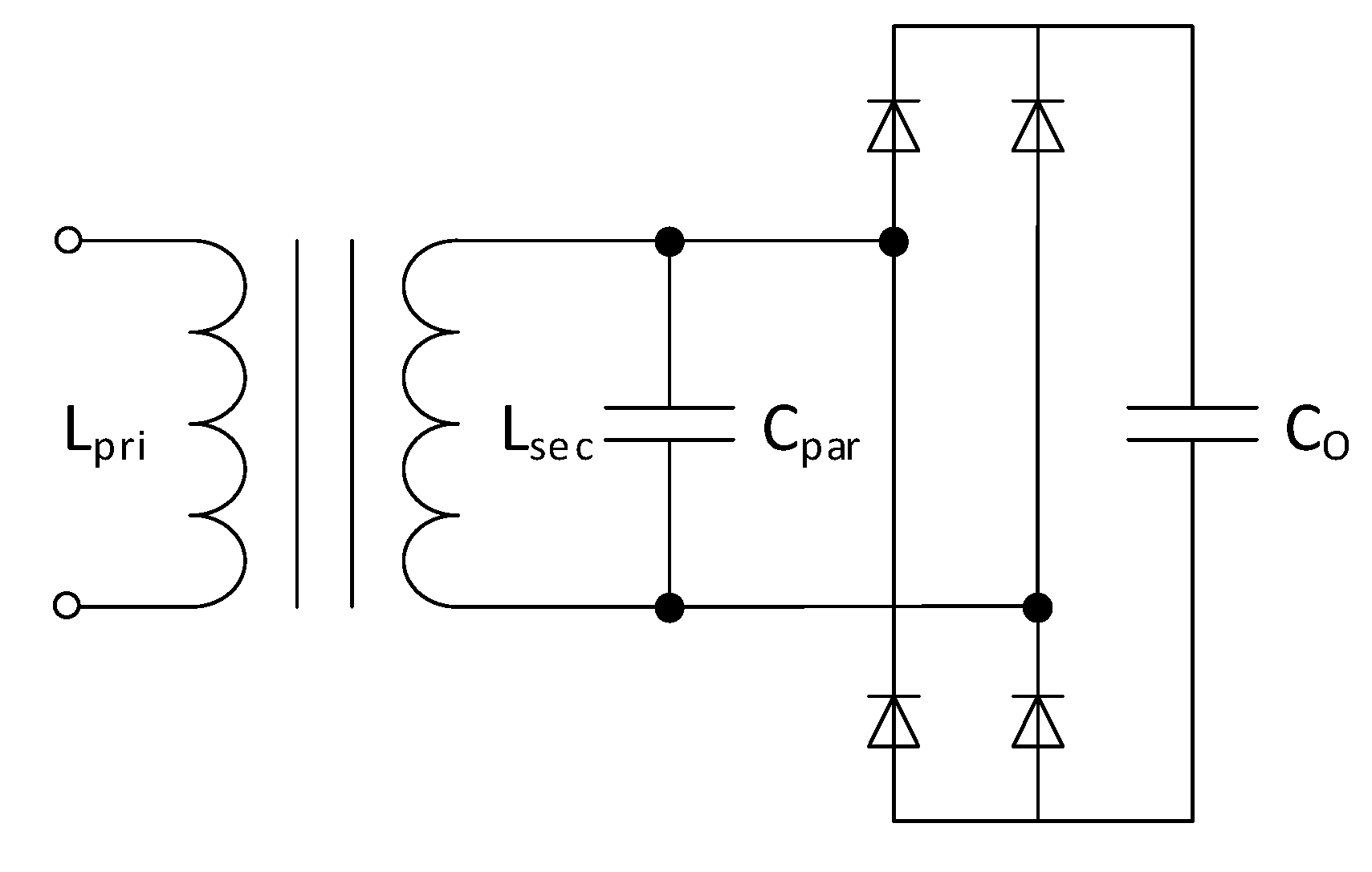
In order to demonstrate this problem, a simplified transformer model was prepared (
Figure 3), in which all of the parasitic capacitances of secondary winding are presented as a one capacitance (Cpar) connected in parallel with this winding [
27,
28,
29,
30]. The primary winding was supplied with 10 V, 10 kHz rectangular voltage. The secondary winding was connected to a discharged 10 nF capacitor by Graetz rectifier.
The simulation was performed in LTSpice—high performance SPICE simulator soft-ware. Despite certain inaccuracies of the built-in models in the program and the developed transformer simplification, the model sufficiently presents the described problem.
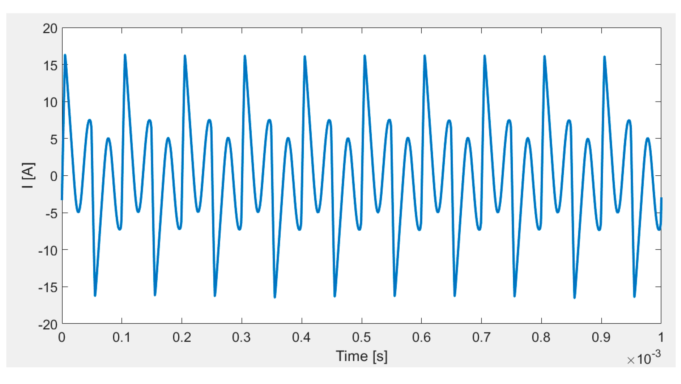
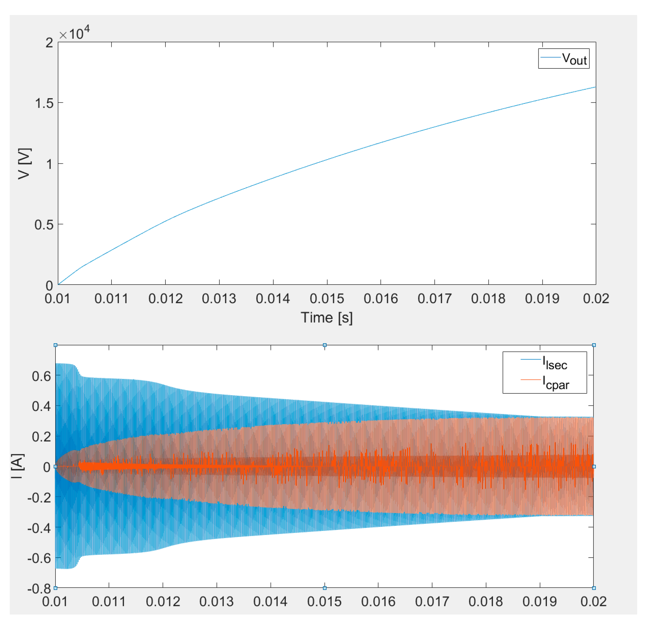
The simulation results (
Figure 4) show that with an increase in output voltage the current used to charge the parasitic capacitances increases, reducing the current that can be used for charging the load capacitor. Thus, the current flowing in the primary winding is increasingly the resonant current flowing between the parasitic capacitances of the secondary winding and the dissipation inductance, and it causes a significant additional load of the transformer and a much greater current flowing in the primary winding, it increases energy losses.
Therefore, many methods have been developed to help at least roughly estimate the capacitances values, both in classical [
24,
31] and simulation [
26,
27,
32] methods, to decrease this problem in transformers through the use of appropriate winding techniques, as well as to predict the possible impact of this phenomenon on the operation of the device, and select the appropriate design.
Based on these considerations, it can be concluded that the self-resonant frequency of the transformer should be raised as high as possible by reducing the parasitic capacitances and inductance of the secondary winding, and thus the winding (in particular the secondary winding) should contain as few turns as possible. Therefore, when designing HV transformers, it is necessary to select cores with the largest possible cross-section area and, at the same time, with the lowest possible AL value.
However, even using this approach, the high number of turns in the secondary winding means that the problem of parasitic capacitance cannot be completely eliminated. As a result, the traditional control methods used in low-voltage switching power converters cannot be used, and this forces a change in the approach to designing HV power supplies [
22].
3. The Problem of Control
As already mentioned, high-voltage high-frequency transformers are characterized by a high current value already in the idle state, because a significant part of the energy supplied to the primary winding is absorbed only for charging the parasitic capacitances in the secondary winding.
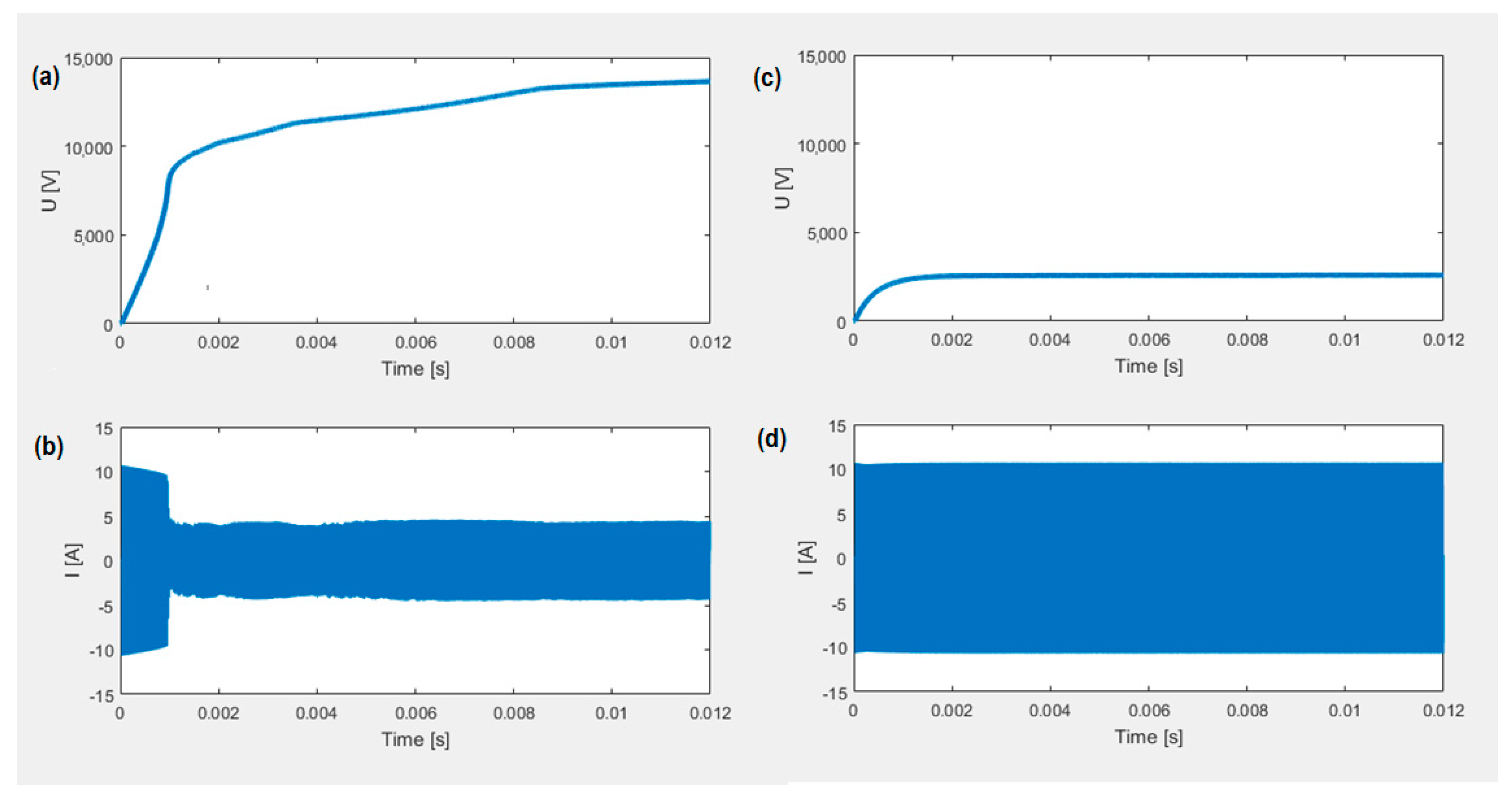
In the case of low-voltage power supplies, the problem of high current in the primary winding is solved by applying a peak or average current limitation, which in fact translates into a reduction in the duty cycle of the signal controlling the operation of the transistors, and thus decreasing the duration of the pulse supplying energy to the transformer. In the case of low-voltage power supplies, this is not a problem. However, in the case of power supplies with a transformer with the problems described, it is not possible to shorten the duration of the pulse supplying energy to the primary winding, because such a power supply may not provide a sufficiently high output voltage. This problem is illustrated by the simulation results presented in
Figure 5, where a model with an idealized transformer was compared to a transformer with parasitic capacitance.
In both cases of the simulations presented in
Figure 5, a peak current limiter was used. The current value of this limitation was set to approximately 12 A. As can be seen in the case of a model in which a transformer without parasitic capacitance was used, this protection worked only at the beginning of the operation of the power supply (
Figure 5a), while in the later phase, even with the maximum duty cycle of the signal controlling the transistors, the current is lower than the value of the protection, and the voltage on the charged capacitor after approximately 12 ms. (
Figure 5b) is approaching the voltage resulting from the transformer ratio and its supply voltage (15 kV). On the other hand, using a transformer model that reflects the real element much more closely, taking into account even a small parasitic capacitance of 10 pF, the current in the primary winding is much higher throughout the whole simulation period (
Figure 5d), the peak current limiter protection works all the time (
Figure 5c), and the voltage on the charged capacitor increases only to approximately 2.5 kV, which is a much lower value than assumed.
The simplest solution to this problem is to increase the value of the current limiter. However, this will result in the flow of a very high current in the primary winding, which may be technically difficult to implement, or not worth doing due to the additional costs of the increase in the cross-section of all connections, or the use of more durable transistors.
4. Quasi-Resonant Algorithm
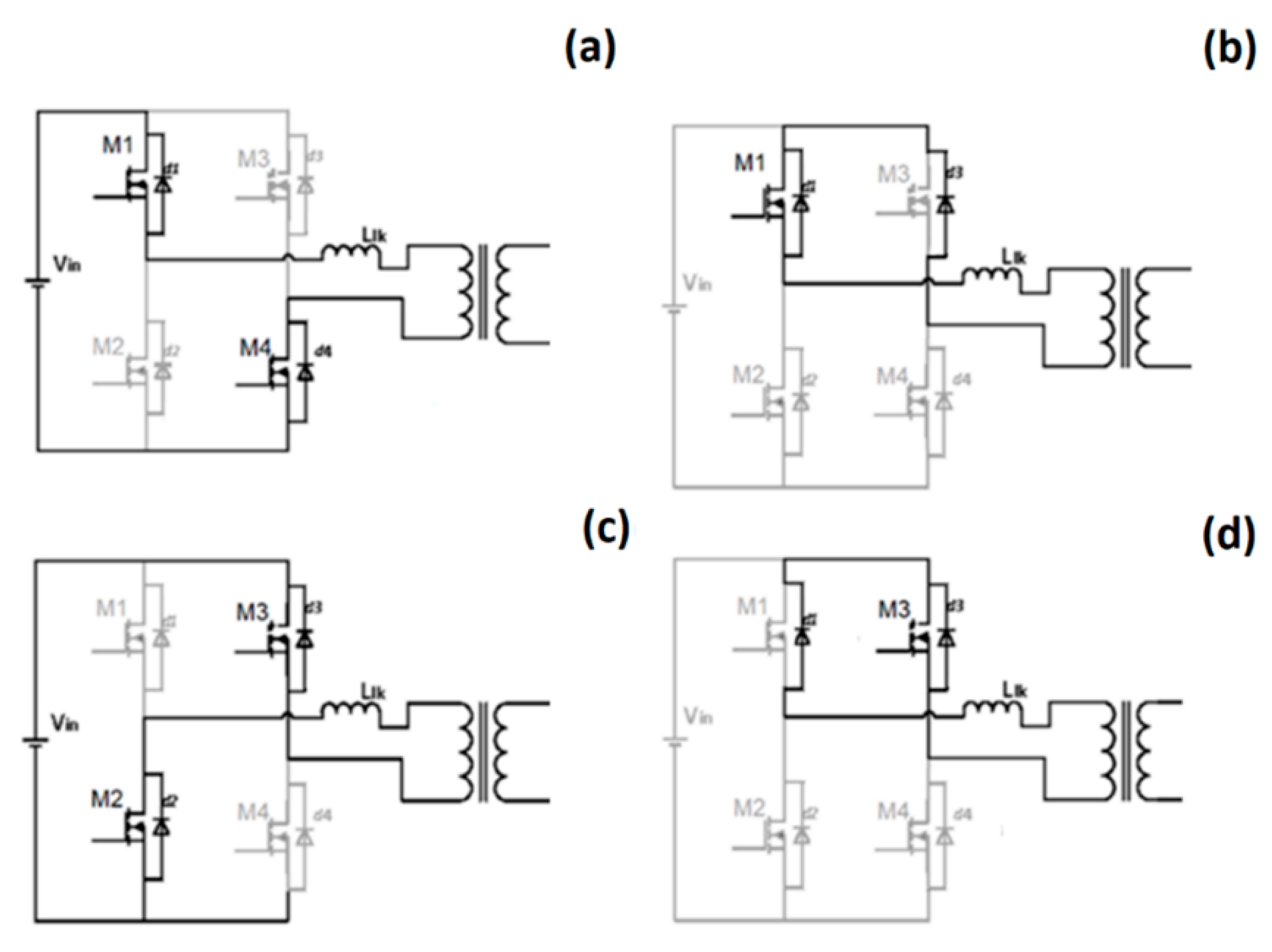
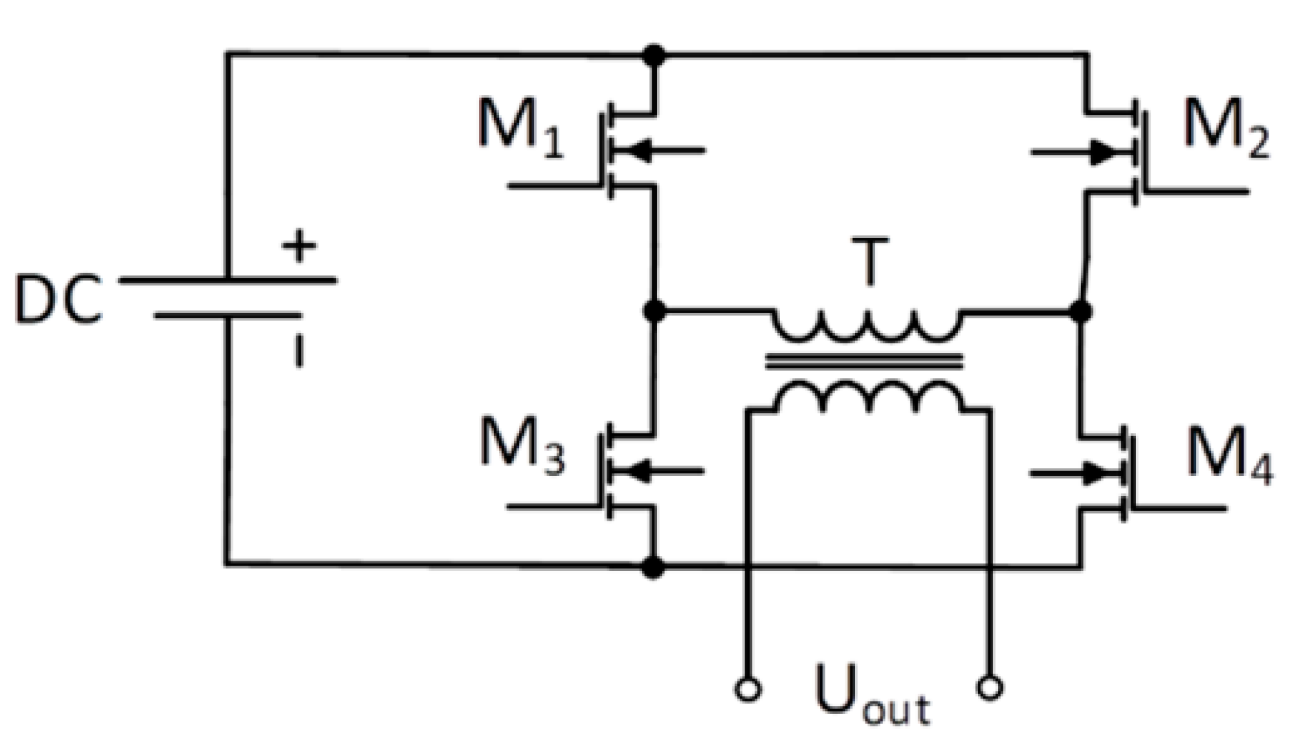
In the presented power supply, a typical full-bridge topology was used (
Figure 6), but to avoid many problems related to the low coupling between primary and secondary windings of the transformer and the large parasitic capacitance, a special transistor control algorithm was developed.
Energy is transferred to the transformer in very short pulses only when a pair of opposing transistors are turned on (
Figure 6—M1–M4 and M2–M3). The duration of these pulses is fixed, which ensures that the energy supplied to the transformer will always be constant. Meanwhile, the value of the current in the primary winding is regulated by the dead time, i.e., the time in which energy is not supplied to the transformer.
The disadvantage of using transformers with a large parasitic capacitance is that large current distortions can occur in the primary winding when using phase-shifted control (
Figure 7). This will cause problems with controlling the current and increase the losses in the windings, making this method difficult to apply.
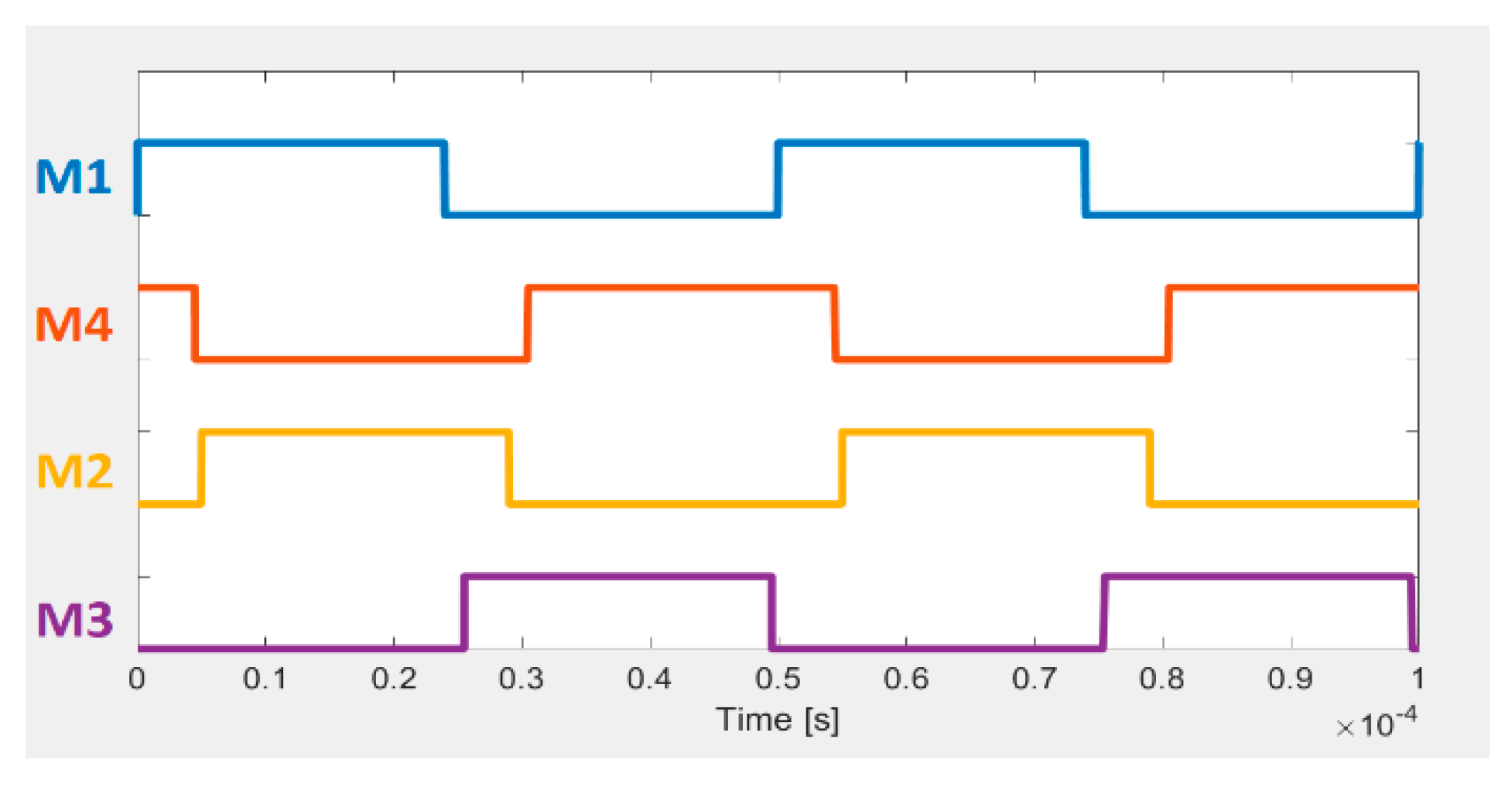
To prevent current distortion in the primary winding, increase the efficiency and reduce electromagnetic disturbances, a modified phase-shifted control was used. In the typical phase-shifted method, a pair of transistors (M1 and M2 or M3 and M4) are switched at almost 50% duty and 180 degrees out of phase with each other. The amount of overlap (phase-shift) between diagonal switches determine the amount of energy transferred to the transformer (
Figure 8). In the developed method, the supply state looks the same, when a pair of diagonal transistors were turned on (
Figure 9a,c). Then, in freewheeling state (in contrast to phase-shifted method), the low side transistor is turned off and only the one high side transistor is still on to ensure a continuous flow of current through the primary winding (
Figure 9b,d).
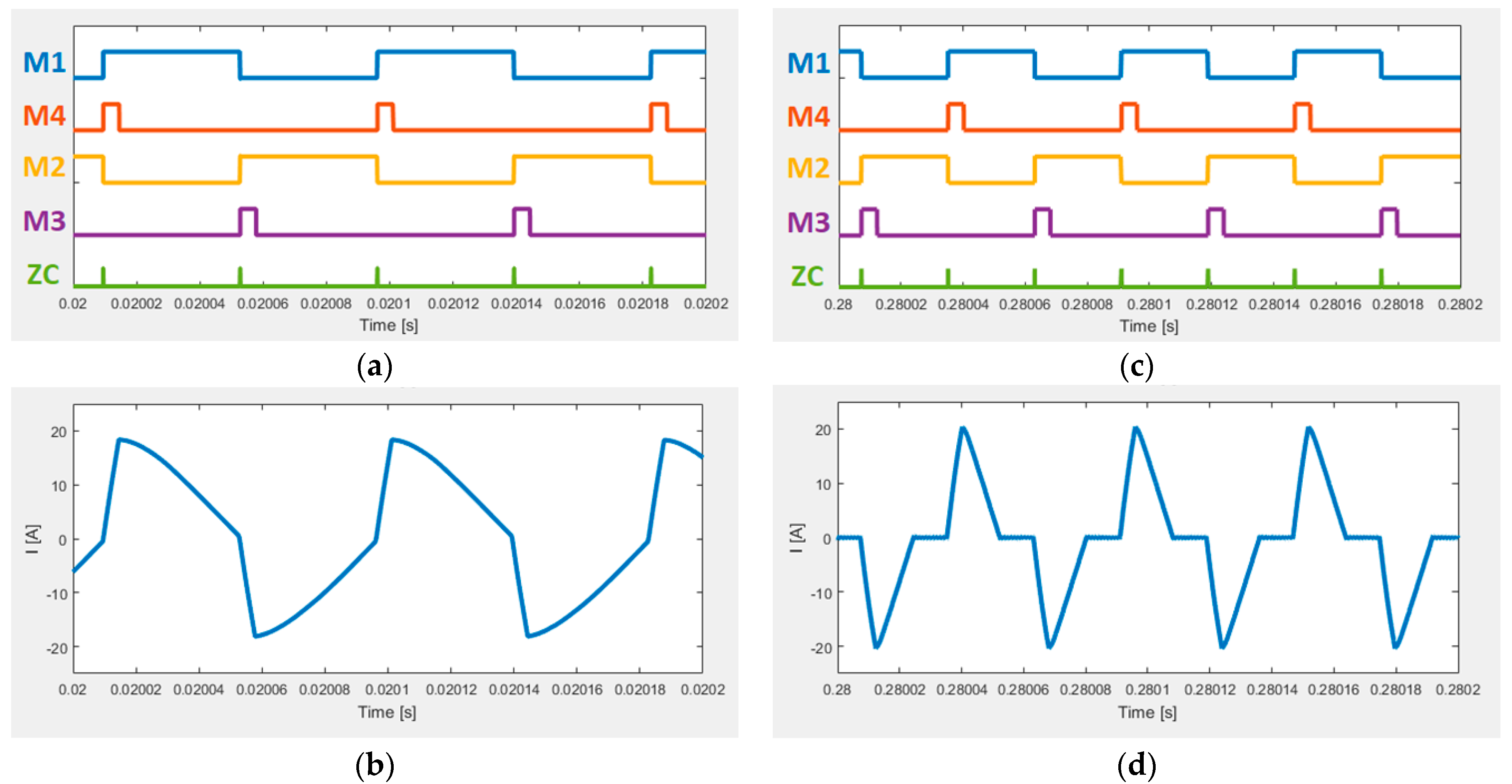
Another modification in relation to the traditional methods is that the freewheeling state is maintained until all of the energy stored in the leakage inductance of the transformer has been transferred to the secondary side, which means that the current in the primary windings drops to zero. After that, the second pair of opposing transistors is switched on and the current starts to flow in the opposite direction through the primary winding. In addition, the developed transistor control algorithm keeps the M1 or M3 (
Figure 6) transistors turned on until the current drops to zero, thus creating a quasi-resonant mode of operation. This approach enables a much better use of the transformer core as in each cycle the magnetic flux density reaches the assumed maximum value.
Figure 10a shows the transistor control signals and an additional signal indicating the drop of current to zero during the first charging state. The current in the primary winding is presented in
Figure 10b.
During this charging phase the transistors are driven with variable frequency dependent on output load and the quasi-resonant algorithm is implemented. However, in this condition there is no possibility to control the charging process. Therefore, a functionality of minimum cycle time has been added. When the load is low (the load capacitor is partially charged) the control algorithm is switched to a fixed frequency, as shown in
Figure 10c,d.
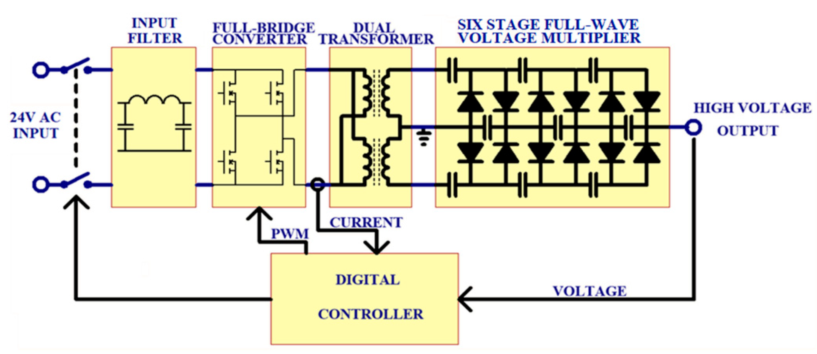
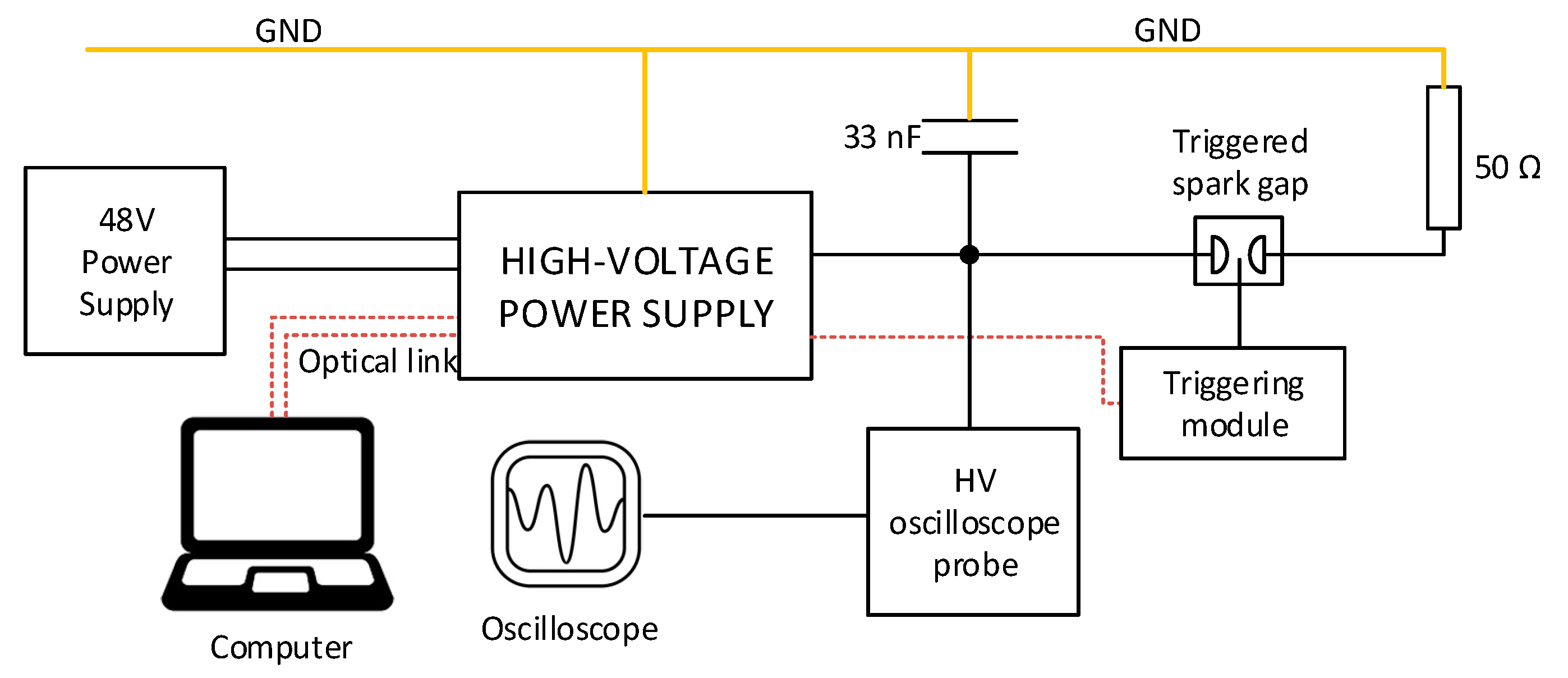
5. High-Voltage DC Power Supply
The block schema of the developed high-voltage power supply is presented in
Figure 11. The use of a voltage multiplier was chosen because it allows us to decrease the output voltage of high-voltage transformers. This solution reduces problems with isolation and parasitic capacitance of the secondary windings.
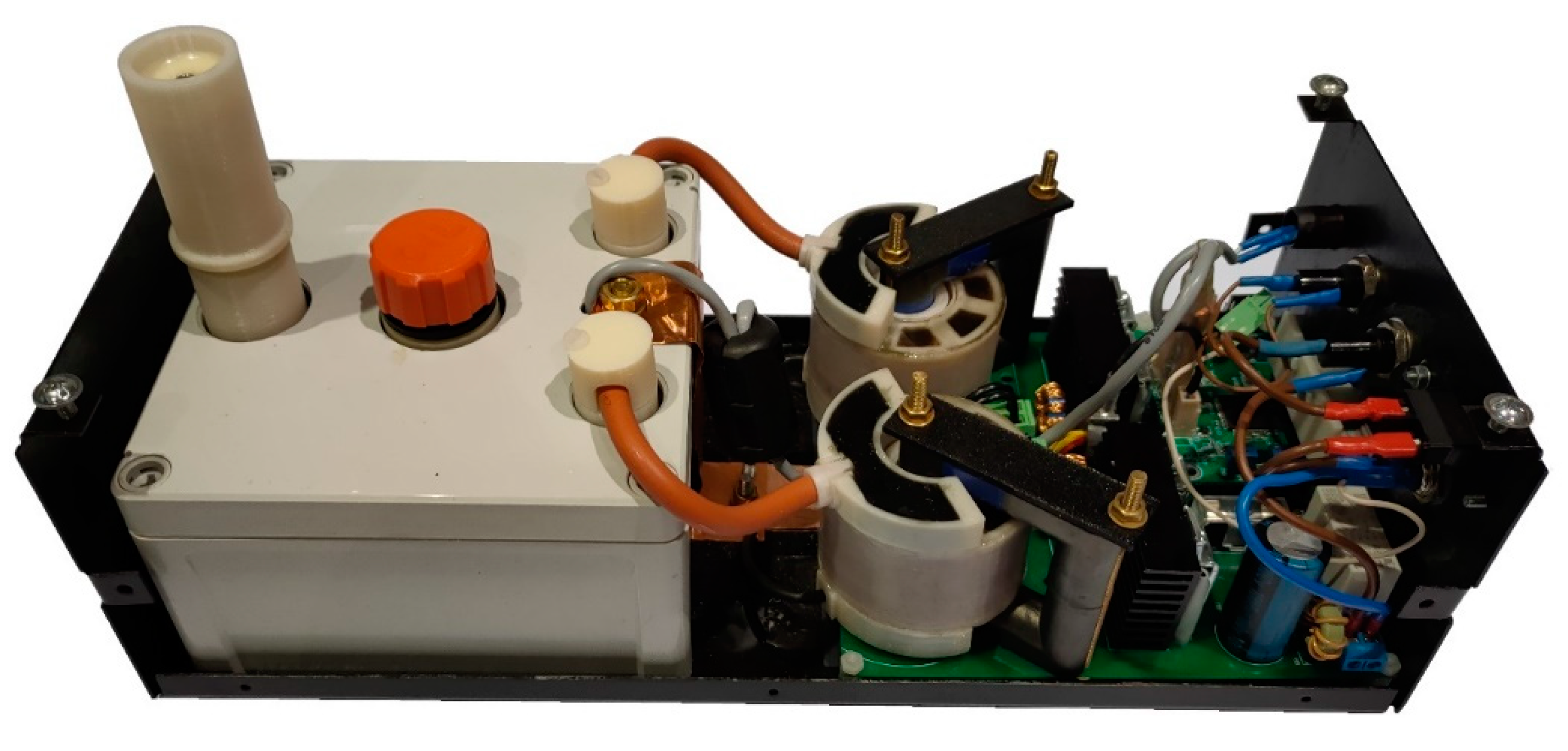
Due to the uniqueness of the presented method, none of the ICs available on the market implement it. Therefore, the digital controller was equipped with a Complex Programmable Logic Device (CPLD) which implemented the developed algorithm and functionalities of peek current limiter and overvoltage protection. This way of implementation was chosen due to fast pin to pin performance of CPLD and the ease of creating even complex logic using a diagram or code. The power supply prepared on this basis is presented in
Figure 12.
The described power supply is designed to work with a 10-stage Marx generator. In each stage, a 3300 pF capacitor was used, giving a net capacity of 33 nF. The assumed frequency of generating pulses is 3 pulses per second at a voltage of 50 kV per stage. Therefore, the power supply should charge the capacity of all stages within a maximum time of 330 ms.
In order to obtain the required parameters, the power delivery state time was set to 5 μs (
Figure 9a,c) and the minimum freewheeling state time (in non-quasi-resonant mode) was set to 20 μs (
Figure 9b,d). A longer time of the power delivery state will saturate the transformer core, while shorter will decrease the power supply performance. The opposite is true with minimum free-wheeling state time—a higher value will decrease the performance but a lower will over-load the power source.
6. Experiments
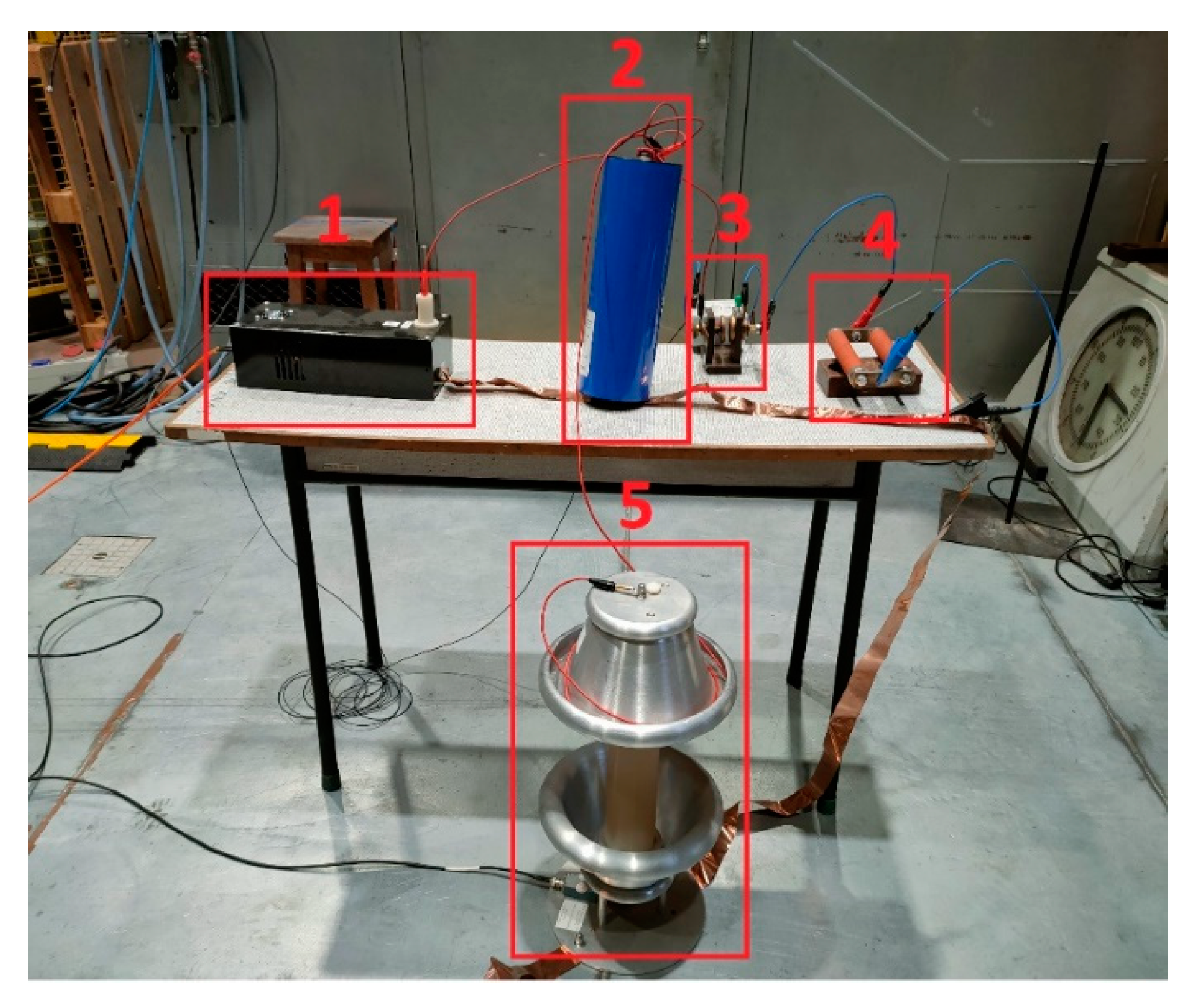
In all the tests performed, a 33 nF high-voltage capacitor was used as a load of the power supply. To measure the output voltage, a high-voltage oscilloscope probe able to measure voltage up to 70 kV DC with a divider ratio of 10,000:1 was used (
Figure 13 and
Figure 14). The accuracy of used high-voltage probe (North Star VD-100) is better than 0.1% for DC voltage and 1% for 10 Hz–1 Mhz range and fully meets the needs for presented measurements.
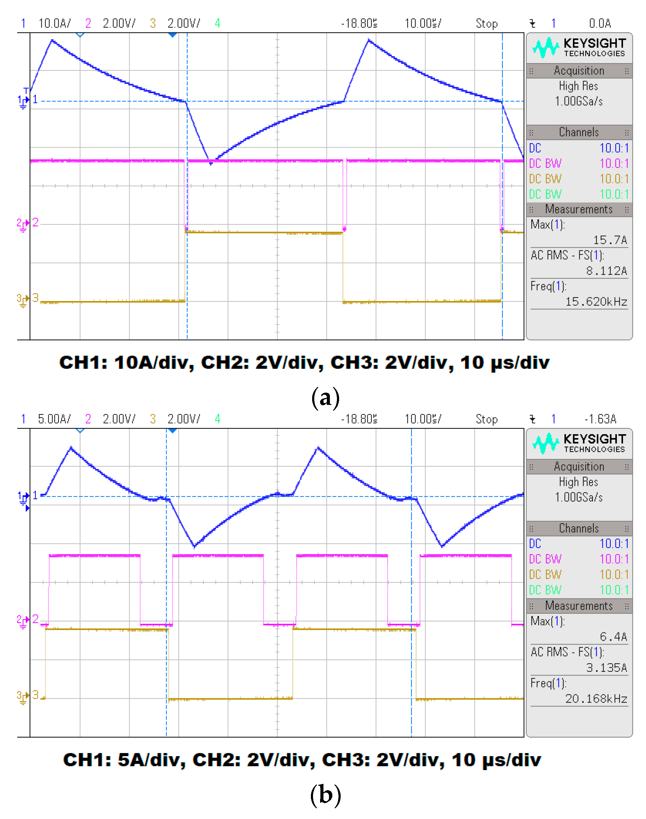
Figure 15 presents the developed transistor control algorithm. At the beginning of the charging process (
Figure 15a) the frequency of the current is approximately 15 kHz and the transistors are switched when the current drops to zero. In a later stage of charging (
Figure 15b), the transistors are switched when the minimal time of one cycle is reached and the frequency of the current is approximately 20 kHz.
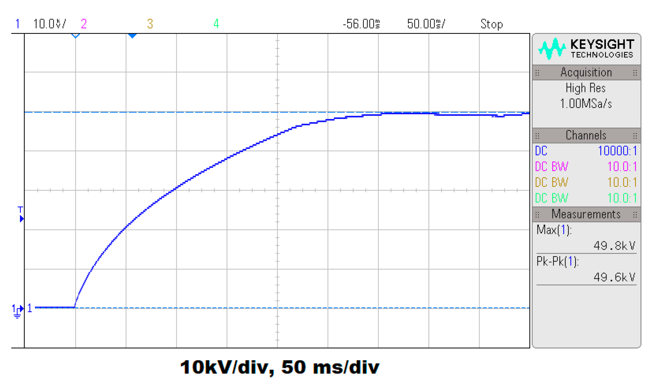
The first test was carried out to demonstrate the charging process. As the test results show (
Figure 16), the charging time up to 50 kV is approximately 300 ms. This value is lower than the required 330 ms.
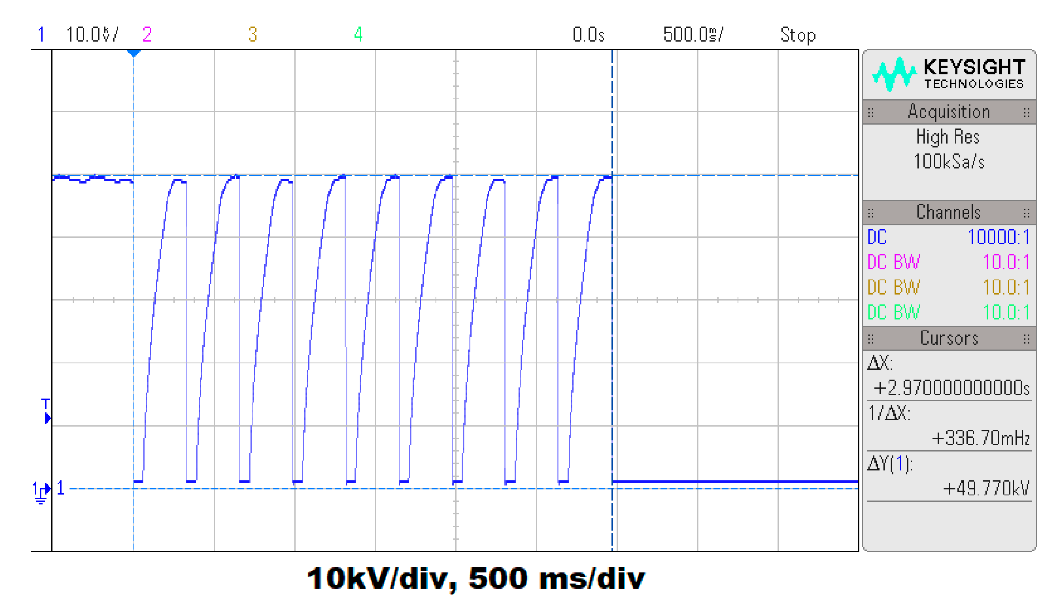
The next test was performed with a sequence of ten discharge-charge cycles. In this test the load capacitor was discharged into a resistive load using a spark gap switch controlled by the power supply. The waveform in
Figure 17 shows the Marx generator recharging process after generating a sequence of pulses. It can be seen that the recharge time is always lower than 330 ms, and after the discharge, the next charging cycle starts automatically.
7. Conclusions
The quasi-resonant control method is very effective for high-voltage power supplies used to charge capacitors. Its use causes almost all the energy supplied to the transformer, which can be stored in the leakage inductance or auxiliary inductance, to be transferred to the load. It also ensures a much better usage of the transformer core (because in each cycle the maximum assumed value of magnetic flux density is reached), reduction in losses on the transistors (in the developed method, two transistors are always switched in a de-energized state) and reduction in electromagnetic disturbances that may be generated when switching off transistors when a current of non-zero value flows in the primary winding, and the use of the CPLD chip greatly facilitates its implementation.
The rather unusual design of the power supply, using a high frequency converter, two high-voltage transformers, a voltage multiplier and a specially developed algorithm can reduce problems related to parasitic capacitance that occur in high-voltage high-frequency transformers while maintaining the required performance.
All the tests carried out showed that the designed power supply fulfilled the assumed requirements when all of the parts were properly designed. The device has a sufficiently high current efficiency, enabling the charging of 33 nF capacitance up to the assumed 50 kV voltage in a time much less than the required 330 ms. The output voltage is very stable and the value set using a dedicated computer program corresponds to the measured value.
The selected solution is easier to implement than those typically used for this purpose, increasing failure-free operation, by reducing the current distortion in the primary winding, and increasing the safety of the device (due to performance of the CPLD). The properties of the multi-stage multiplier allow for the easy expansion of the capabilities of the power supply by adding voltage multiplier stages and easily adapting the power supply to different requirements.

