Article

Research on ZVS Phase-Shifted Full-Bridge Broadband Inverter Based on Auxiliary Current Source

School of Automation, Wuhan University of Technology, Wuhan 430070, China
*
Author to whom correspondence should be addressed.
Energies 2022, 15(22), 8661; https://doi.org/10.3390/en15228661
Submission received: 29 September 2022 / Revised: 10 November 2022 / Accepted: 15 November 2022 / Published: 18 November 2022
(This article belongs to the Special Issue Design, Optimization and Applications of Power Converters)

Abstract

:
Phase-shifted full-bridge topologies are widely used in medium- and high-power DC/DC converters due to their small size and high switching frequency. However, there are few studies on the application of broadband inverters. In the traditional phase-shift full-bridge inverter with a fully resonant load, the problem of current commutation which leads to hard switching is often encountered, to overcome such an issue, an auxiliary current source network is introduced to realize the zero-voltage turn-on of the lagging bridge arm. The working modes of the converter are analyzed in detail, and the parameters of the auxiliary current source network are designed. The simulation verification is carried out by MATLAB/Simulink in a wide frequency range from 10 kHz to 500 kHz. Finally, an experimental circuit board is designed, and the experimental results show that the topology can achieve soft switching in a frequency range from 10 kHz to 200 kHz and has a certain applicability.

1. Introduction

In recent years, with the rapid development of power electronics technology, various electrical equipment are increasingly inseparable from switch converters. The development of this technology also puts forward higher requirements on the performance, weight, volume, efficiency and reliability of the switch power supply. If the voltage and current waveforms overlap during the turn-on and turn-off of the switching device, it is called hard switching. As the operating frequency increases, the number of hard switching per unit time increases, and the loss of the inverter increases accordingly [1,2,3]. To reduce the loss, soft switching technology emerges as the time required. Many scholars have successively proposed resonant converter (RC), quasi-resonant converter (QRC) and multi-resonant converter (MRC) [4,5,6], which realize the zero-voltage soft switching or zero-current soft switching of the transistors, reduce the switching loss, improve the efficiency of the converter, greatly improve the switching frequency, and reduce the volume and weight.
The full-bridge inverter circuit is the most widely used topology in single-phase inverter power supplies, with the advantages of a simple, symmetrical structure and a flexible, simple control method. Using the full-bridge high-frequency inverter topology in the high-frequency power supply can obtain higher efficiency. According to the different turn-on signals of the switching devices, the common control methods of the full-bridge converters include bipolar control methods, finite unipolar control methods and phase-shift control methods. In the phase-shifted full-bridge control method, the current and voltage stress of the switching device is small, which is easier to realize soft switching, the load circuit itself has a good filtering effect, and the switching frequency remains unchanged, avoiding the problem of frequency runaway. Since the phase-shift control method has the above advantages, this paper chooses the phase-shift control method [7].
At present, the full-bridge circuit using phase-shift control has been deeply studied in various situations: in biological applications, the article [8] proposed a high-frequency high-voltage composite pulse generator, in which eight switches are connected in series on one bridge arm. To study the mechanism of tumor ablation under the high-frequency composite pulse and reduce the number and intensity of muscle contractions, the transistor generates a composite pulse with a frequency of 2 MHz and a pulse amplitude of 3 kV. In terms of induction heating, the article [9,10] uses the principle of induction heating to propose a power control scheme of a series resonant full-bridge inverter to heat cookware at a frequency of 35 kHz. The article [11] presents a novel high-performance high-frequency soft-switching inverter for induction heating applications. For multiple load induction heating applications, the article [12] proposed a three-switch inverter composed of only three switches and two split capacitors. Asymmetric duty cycle control is used to obtain independent control over two loads simultaneously. In addition to the structure of the inverter, research on the control method is also essential. The article [13] proposed a new control method for induction cookware applications with a series resonant inverter, which simplified the design of the control circuit. However, this method used a sampling circuit, which could bring some interference to the experimental results. In the article [14], an extended series-resonant inverter (SRI) with the output current control based on the pulse-density-modulation (PDM) control technique has been presented. The disadvantage of the PDM control technique is that it can lead to different output current amplitudes. Due to the soft switching characteristics of the full load range, the inverter has low EMI noise and high efficiency, which can be suitable for higher frequency induction heating applications. In terms of wireless energy transmission, in the article [15], a magnetically coupled resonant wireless transmission method is proposed, and a 1.2 kW/48 V prototype is built by taking advantage of the phase-shifted full-bridge soft-switching technology, which not only realizes the soft-switching of the full-bridge circuit but also improves the transmission efficiency of the wireless transmission system.
Of the above applications, most of them are designed for a single switching frequency. Less research has been done in applications where a broadband switching frequency is required, such as driving Helmholtz coils for magnetic field probe correction [16]. When the phase-shifted full-bridge inverter is connected to the RLC series resonant load, the current in the switching device sometimes flows in the reverse direction. At this time, the turn-off signal cannot effectively turn off the switching device, resulting in hard switching. The topology of a ZVS phase-shifted full-bridge inverter based on an auxiliary current source is used to achieve soft switching by injecting a current into the switching devices to charge their parallel capacitors. The relationship between the parameters of the auxiliary current source network and the frequency band used for soft switching is studied.
The remainder of this paper is organized as follows. The inverter circuit and its working modes are analyzed in Section 2. In Section 3 and Section 4, a simulation model is built and analyzed, and a 30 V input and 18.2 V/1.2 A output prototype was designed and tested to verify the feasibility of this topology. Finally, the conclusion is drawn in Section 5.

2. Full-Bridge Inverter Circuit and Its Working Modes Analysis

2.1. Full-Bridge Inverter Topology

The circuit topology used in this paper is shown in Figure 1. The circuit consists of a typical full-bridge inverter circuit and an auxiliary injection current source. For the Full-bridge inverter circuit, VDC is the DC input voltage source, Q1–Q4 are power MOSFETs, Q1 and Q3 form the leading bridge arm, Q2 and Q4 form the lagging bridge arm, and the two transistors on the same bridge arm cannot be simultaneously conducted, otherwise, it will cause a short circuit to the DC voltage source, so that the current flowing through the transistors is too large, and the components will be burned. L, C and R are resonant inductance, resonant capacitance and resistive load, respectively. During operation, L and C resonate in series, so that the load current presents a sine wave. For the auxiliary current source [17], the network consists of auxiliary inductance La, auxiliary diodes Da1, Da2 and auxiliary capacitors Ca1, Ca2. The auxiliary inductor La is connected to the midpoint of the lagging bridge arm and the midpoint of the bridge arm formed by the auxiliary diodes Da1 and Da2.
The drive signals of four switches Q1–Q4, the waveforms of the AB port voltage uAB, and the load current io are shown in Figure 2. The main waveform diagram of the auxiliary current source network is shown in Figure 3. It can be seen that the conduction signals of the switches on the same bridge arm are 180° complementary (to ensure soft switching, a certain dead time is set), the difference between the driving signals of the switches at the diagonal position, i.e., the phase shift angle, and the output voltage can be adjusted by adjusting the size of the phase shift angle θ.
Within one cycle, the expression for the output port voltage is:
u A B = { 0 , 0 < ω t < θ , π < ω t < π + θ V D C , θ < ω t < π V D C , π + θ < ω t < 2 π
Fourier decomposition of this voltage waveform yields:
u A B = n = 1 4 V D C n π cos n θ 2 sin ( n ω t ) , n = 1 , 3 , 5
Then, its fundamental component is:
u A B 1 = 4 V D C π cos θ 2 sin ( ω t )
If ω is the resonant angular velocity of the LC load, i.e.,
ω = ω 0 = 1 L C
Then, at this angular velocity, the RLC load can be regarded as a purely resistive load. So, the current io flowing through the load is:
i o = 4 V D C R π cos θ 2 sin ( ω t )

2.2. Circuit Working Modes Analysis

When the load works at the resonant frequency, the waveforms of the port voltage uAB and the load current io are shown in Figure 2 [18]. The waveform analysis of the circuit topology shown in Figure 1 is presented, and the following assumptions are made to facilitate the analysis:
  • All switches and diodes are ideal devices. The conduction voltage drop of the diode is vd.
  • All inductors and capacitors are ideal devices.
  • C1 = C2 = C3 = C4 = Cp, Ca1 = Ca2 = Ca.
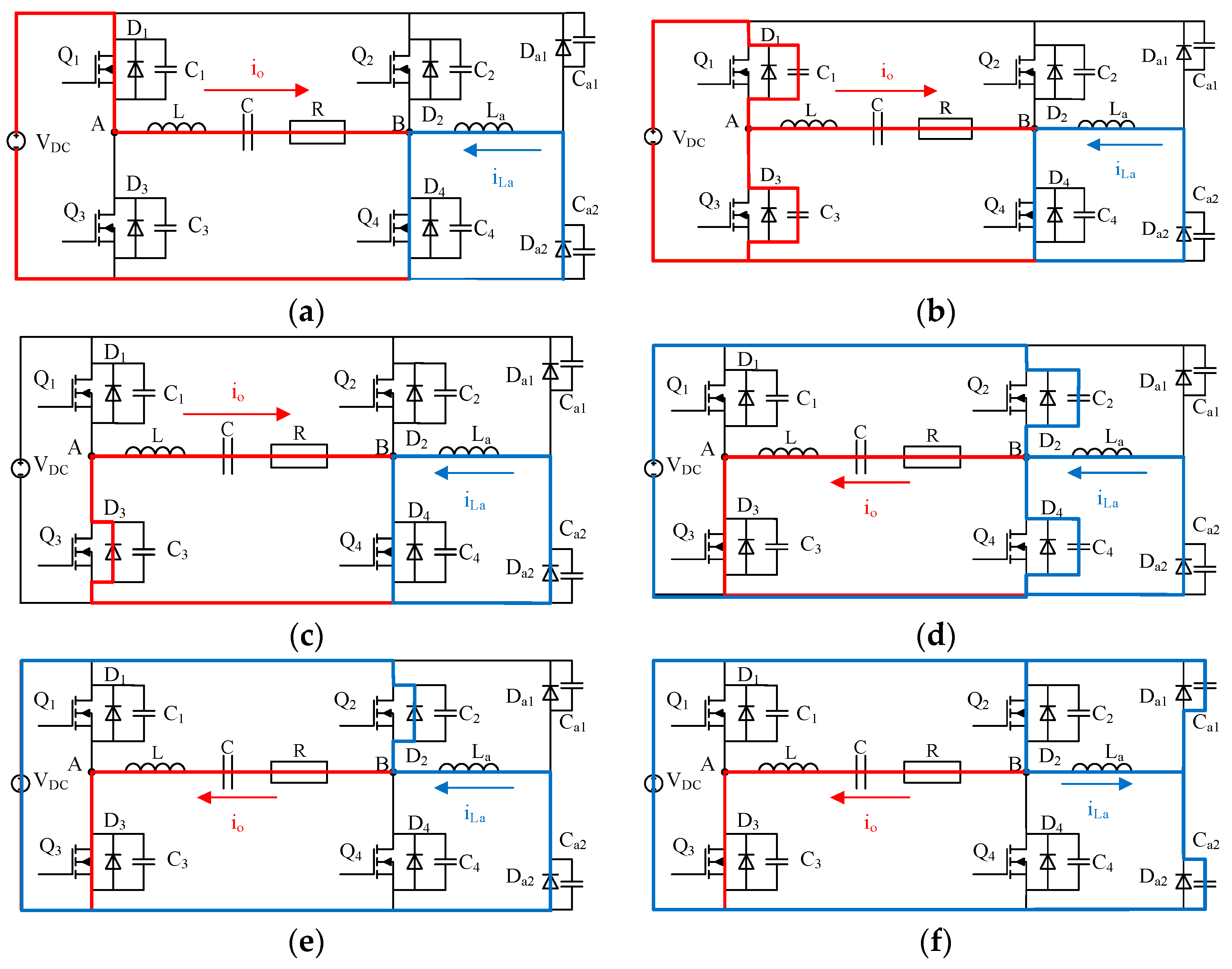
Switching mode 1 (t0–t1): At time t0, Q4 is turned on. The voltage of port AB is the power supply voltage VDC, and the current io flows from the power supply through Q1, resonant inductor L, resonant capacitor C, resistor R and Q4, and finally returns to the power supply, and this mode lasts until time t1. The injection current iLa flows through the auxiliary diode Da2, the auxiliary inductance La, and the switch Q4 to form a loop, which corresponds to Figure 4a.
Switching mode 2 (t1–t2): At time t1, Q1 is turned off. Due to the freewheeling effect of the resonant inductor L, the current will be transferred from Q1 to the capacitors C1 and C3 of the switches, charging C1, whereas discharging C3 at the same time. The voltage of point A will gradually decrease. When it drops to zero, D3 will be turned on naturally, and then the turn-on signal of Q3 will come at time t2, realizing the zero-voltage turn-on of Q3. The injected current keeps the path of the previous mode, which corresponds to Figure 4b.
During the charging process of C1, by KVL, there are:
v C 1 + v C 3 = V D C
The derivative of the voltage is:
d v C 1 d t = d v C 3 d t
Because i C = C d v C d t , there are:
i C 1 = i C 3 = 1 2 i o
Because in switching mode 2, the amount of current change is small, it may be considered that the current during this period is constant, and its value is the current value at time t2. Then, there are:
i C 1 ( t 2 ) = i C 3 ( t 2 ) = 1 2 i o ( t 2 ) = 2 V D C R π cos θ 2 sin θ 2
Switching mode 3 (t2–t3): Q3 is turned on at time t2. Although Q3 is in on state at this time, the current does not flow through Q3, but freewheels through D3, which is naturally turned on. Since Q4 is also in on state, the voltage across port AB is zero, and this mode lasts until time t3. In this switching mode, the load current changes from positive to negative. The injected current path continues to remain unchanged. This mode corresponds to Figure 4c.
Switching mode 4 (t3–ta): Q4 is turned off at time t3. Since the current has commutated at this moment, if there is no injection current iLa, the load current will flow through D4 for freewheeling, realizing zero-voltage turn-off of Q4. However, in this mode, no current flows through capacitor C4, which cannot be charged, so the voltage at point B remains zero. When Q2 is turned on, the voltage at point B is forcibly pulled high, and the zero-voltage turn-on of the lagging bridge arm is not realized. Additionally, when 1/2 of the injected current iLa at this moment is greater than the load current at this moment, C4 can be charged, creating conditions for the soft switching of the lagging bridge arm. The injection current path is shown in Figure 4d.
Note the magnitude of the injected current iLa(t3) at time t3 as iLal. When charging and discharging the capacitor, it is approximately considered that the current keeps iLal unchanged. Then, in the process of charging and discharging, there are:
0.5 ( i L a l i o ) = C p d v C 4 d t
Then, the charging and discharging duration t3a is:
t 3 a = C p V D C 0.5 ( i L a l i o )
If the time is less than the dead time, the soft switching of the lagging bridge arm can be guaranteed.
Switching mode 5 (ta–t4): At time ta, after charging and discharging the lagging bridge arm capacitor by the injected current in the previous mode, the voltage at point B rises to the power supply voltage, and D2 is naturally turned on. The main circuit and the flow of the injected current are shown in Figure 4e. Since the voltage across the auxiliary inductor La is the power supply voltage at this time, the injection current iLa will decrease with the slope of −VDC/La, and the injection current will decrease to zero for ta4:
t a 4 = L a i L a l V D C
Switching mode 6 (t4–tb): At the moment of t4, the switch Q2 is turned on. Since its body diode D2 is naturally turned on, it leads to zero-voltage turn-on. The main circuit and the flow of the injected current are shown in Figure 4f. The injected current is commutated, the auxiliary inductor La and the auxiliary capacitors Ca1 and Ca2 work in resonance, iLa charges Ca2 and discharges Ca1 at the same time.
The injected current iLa and the voltages of Ca1 and Ca2 in this period are:
i L a ( t ) = V D C Z a 2 sin ω a ( t t 4 )
v C a 1 ( t ) = V D C cos ω a ( t t 4 )
v C a 2 ( t ) = V D C cos ω a ( t t 4 ) + V D C
where ω a = 1 / 2 L a C a , Z a = L a / ( 2 C a ) . The time required to charge the auxiliary capacitor Ca2 is:
t 4 b = π 2 2 L a C a
At time tb, the injected current is:
i L a ( t b ) = V D C Z a
The injected current at this moment is denoted as iLah. As can be seen from Figure 3, the slope of the auxiliary inductor current changes in a sinusoidal manner, so the auxiliary inductor voltage will not have a large mutation.
After time tb, the auxiliary diode Da1 is naturally turned on, and the injection current iLa flows through the switch Q2, the auxiliary inductance La, and the auxiliary diode Da1 to form a loop. Due to the conduction voltage drop vd of the diode, the auxiliary inductor current will gradually decrease, and the slope of the current decrease is vd/La. Until the time t7, the switch Q2 is turned off, and the second half cycle begins, and the analysis is similar to the first half cycle. In order to save space, it will not be described in detail here.
From the above analysis, it can be concluded that:
  • To realize the soft switching of the leading bridge arm, it is necessary to ensure that the current flowing through the capacitor can charge the capacitor to the power supply voltage VDC within the dead time. According to i C = C d v C d t , combined with (9), the time required to charge the capacitor to the power supply voltage VDC can be obtained as:
    t r = C p R π sin θ
    This time is less than the dead time to ensure soft switching.
  • To realize the soft switching of the lagging bridge arm, it is necessary to ensure that the charging and discharging time t3a of the lagging bridge arm is less than the dead time.
  • The maximum value iLah of the auxiliary inductor current iLa is only related to the parameters of the DC voltage source and the auxiliary network, i L a h = V D C Z a = V D C L a / ( 2 C a ) , therefore, as long as the parameters of the auxiliary network are determined, the magnitude of the current injected into the desired bridge arm can be determined.
  • The voltage stress of the auxiliary capacitor is the DC voltage source voltage VDC.
  • The voltage stress of the auxiliary diode is VDC and its current stress is iLah.
  • When Q4 (or Q2) is off, the auxiliary inductor current iLa flows into (or out of) node B. Its amplitude is:
    | i L a l | = V D C L a / ( 2 C a ) v d L a t c
    where t c = 1 2 f ( t 3 a + t a 4 + t 4 b ) .

2.3. Applicable Frequency Range

When the frequency decreases, the current iLal injected by the auxiliary current source decreases due to the extended time that the conduction voltage drop of the auxiliary diode acts on the auxiliary inductor. When the frequency increases, the switch Q2 (or Q4) will be turned off when the auxiliary capacitor Ca2 is fully charged (or discharged), so that the injection current is maximized. Therefore, as long as the injection current iLal and the maximum current iLah are slightly larger than iLal, a certain frequency range can be found, so that the parameters of the auxiliary current source designed in this paper can achieve soft switching within this range.
Calculation of the lowest frequency: When the injected current drops from iLah to iLal, the corresponding switch will act. According to the current falling time, resonance time and linear falling time, the lowest frequency can be calculated. Since iLah and iLal are given, the current falling time tc can be calculated:
t c = ( i L a h i L a l ) L a v d
The lowest frequency fL can be calculated by substituting (20) into (19):
f L = 1 2 ( t 01 + t 12 + t 23 + t c )
Calculation of the highest frequency: When the resonance of the auxiliary inductor and capacitor is completed, the corresponding switch will act when the injected current is the largest. From the resonance time and the linear falling time, the highest frequency fH can be calculated:
f H = 1 2 ( t 01 + t 12 + t 23 )
Therefore, for the auxiliary inductance La, the auxiliary capacitance Ca can be calculated from iLah and (17). Then, the applicable frequency range of soft switching corresponding to the parameters of the auxiliary current source can be obtained.

3. Simulation Results Analysis

3.1. Simulation Parameter Setting

The DC voltage source used in the simulation is VDC = 30 V, the load inductance L is set to 1 mH, and the load resistance R is 15 Ω. The load capacitance C working in the resonance state can be determined by (4):
C = 1 4 π 2 f 2 L
Set the dead time to 100 ns. To realize the adjustable ability of the load current, the phase shift angle θ needs a certain adjustment range. In this paper, the range of the phase shift angle θ is set to 10°–170°. According to (18), when the switch Q1 is turned off, the time required for C1 to charge to the power supply voltage is:
t r = C p R π sin θ = 15 π sin θ C p
In order to ensure that the phase shift angle θ is in the range of 10°–170°, the leading bridge arm can achieve soft switching, it is necessary to take θ 10° (or 170°) when the calculated charging time tr is less than the dead time 100 ns. Setting Cp = 350 pF in this paper. In this case, the load current when switch Q1 is turned off is 0.22 A.
For the lagging bridge arm, according to Figure 2, the current magnitude of the load current io when Q4 is turned off |io(t3)| is slightly smaller than the current magnitude |io(t4)| when Q2 is turned on. From the symmetry of the sine function and (9), the magnitude of the reverse load current |io(t3)| when Q4 is turned off can be calculated:
| i o ( t 3 ) | | i o ( t 4 ) | = | i o ( t 2 ) | = 2 V D C R π sin θ
To ensure that the injected current can compensate for the reverse load current within the required phase shift angle and to charge and discharge the parallel capacitor of the lagging bridge arm, the maximum reverse load current is required when Q4 is turned off, i.e., the phase shift angle θ is 90°. The maximum reverse load current when Q4 is turned off is obtained by (25) as 1.27 A. It has been deduced before that the minimum load current required for charging and discharging the parallel capacitor of the switch is 0.22 A, with a certain margin, the iLal of the injected current source is set to 2 A.
Taking the maximum injection current iLah as 3 A, and using (11), (17) and their corresponding analysis, there are:
t 3 a = C p V D C 0.5 i L a l i o 100   ns
C a = i L a h 2 2 V D C 2 L a
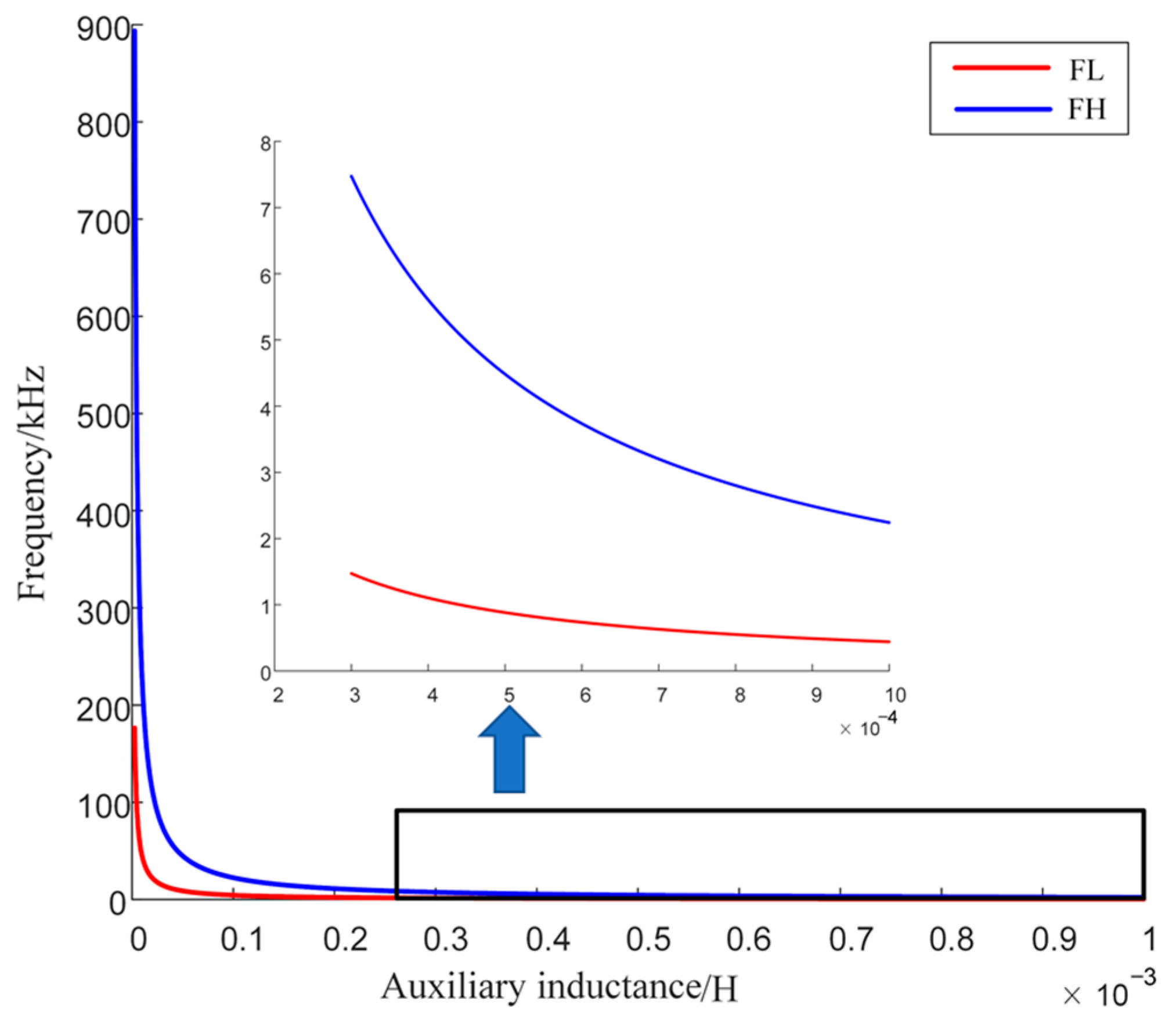
For the calculation of the lowest and highest frequencies, from the parameters given by the simulation and (21), (22), the relationship between the lowest frequency, the highest frequency and the auxiliary inductance can be obtained as:
f L = 1 2 ( 2 × 10 9 + 1.132 L a )
f H = 1 2 ( 2 × 10 9 + 0.223 L a )
The relationship between the two frequencies and the auxiliary inductance is shown in Figure 5, it can be seen that the smaller the auxiliary inductance, the higher the frequency range in which the auxiliary current source can achieve soft switching. However, the minimum frequency at which a smaller auxiliary inductor can achieve soft switching is still very large. Therefore, to achieve the widest possible range of soft switching, it is necessary to use multiple sets of auxiliary inductor-capacitor parameters.
In order to realize the soft switching in the frequency range of 10 kHz–500 kHz, the selected auxiliary inductance and capacitance parameters are shown in Table 1. For example, when the LC parameter of number 1 is selected, soft switching can be realized in the range of 10–50 kHz, which is the advantage of the auxiliary circuit. By changing the number of the auxiliary circuit, the frequency range of the soft switching can be broadened.

3.2. Simulation Circuit and Results Analysis

According to the parameters in the previous section, the simulation model of the phase-shifted full-bridge inverter is built using MATLAB/Simulink simulation software, as shown in Figure 6.
In this circuit, switches connected in series are used to realize the access of the corresponding auxiliary current source. Once the switching frequency is determined, three switch sets Sa, Sb and Sc are used to select appropriate auxiliary circuits to help achieve soft switching. When the switching frequency is in the range of 10 kHz to 50.80 kHz, only the switch set Sa corresponding to the auxiliary current source of serial number 1 is turned on, so that it is connected to the circuit; when the switching frequency is in the range of 50.80 kHz to 257.50 kHz), only the switch set Sb is turned on to involve the auxiliary current source of serial number 2. When the switching frequency is 257.50 kHz to 500 kHz, only the switch set Sc is turned on, and the auxiliary current source of number 3 is connected to the circuit. The switching frequency of the inverter remains unchanged during operation, so the state of the switch sets Sa, Sb and Sc also remains unchanged. As the bidirectional switch controlling the auxiliary circuit is always on, the loss is almost only conduction loss, which is a small part of the total loss. By selecting the connected auxiliary current sources according to the frequency range, a broadband zero-voltage soft-switching can be achieved.
Taking 90° phase shift angle as an example, set the simulation parameters as follows: switching frequency f = 10 kHz, dead time 100 ns, DC voltage source VDC = 30 V, voltage source series resistance Rs = 0.01 Ω, load inductance L = 1 mH, load resistance R = 15 Ω, load capacitance C = 253.3 nF, the parallel capacitance of the switch Cp = 350 pF.
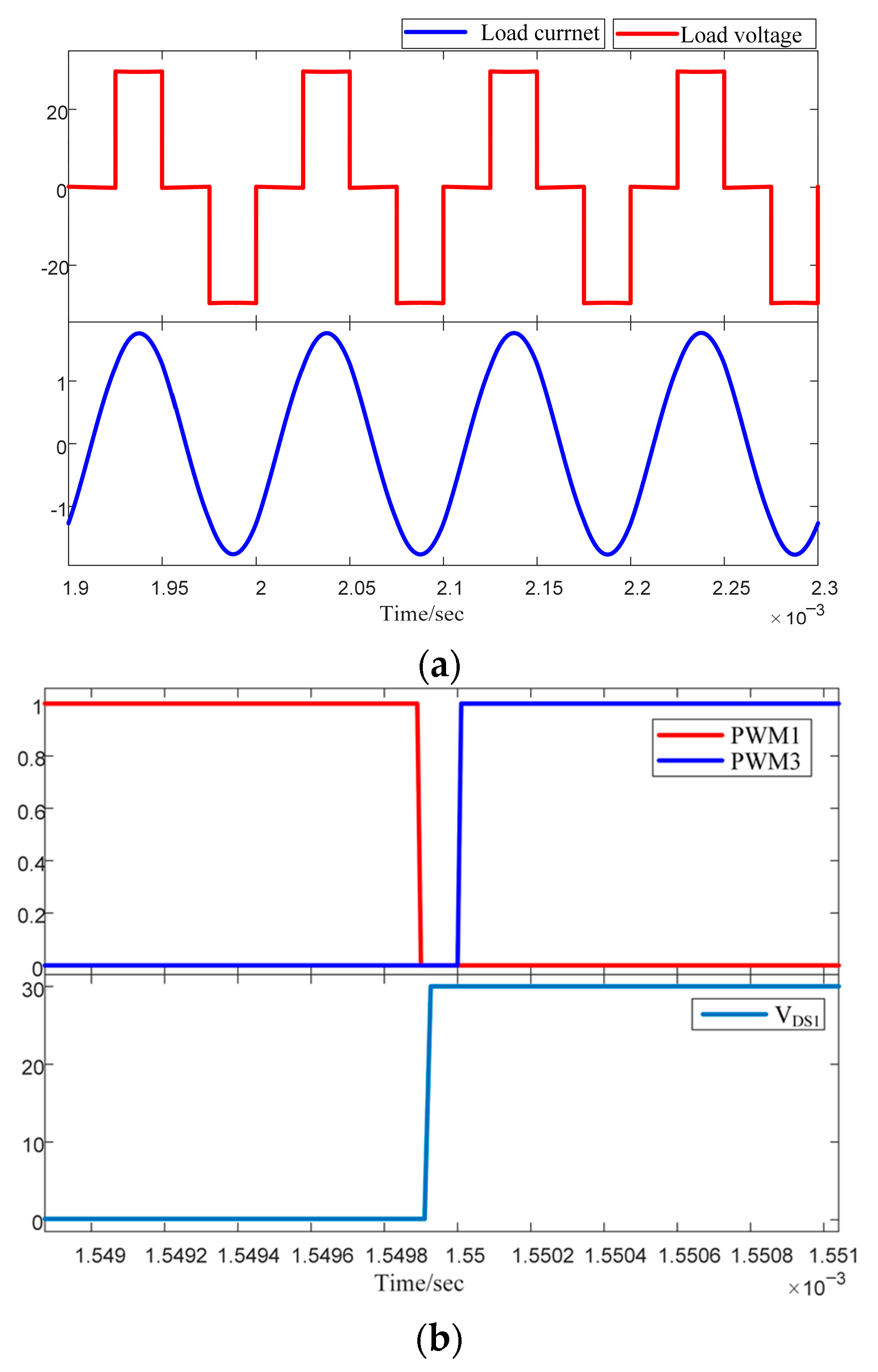
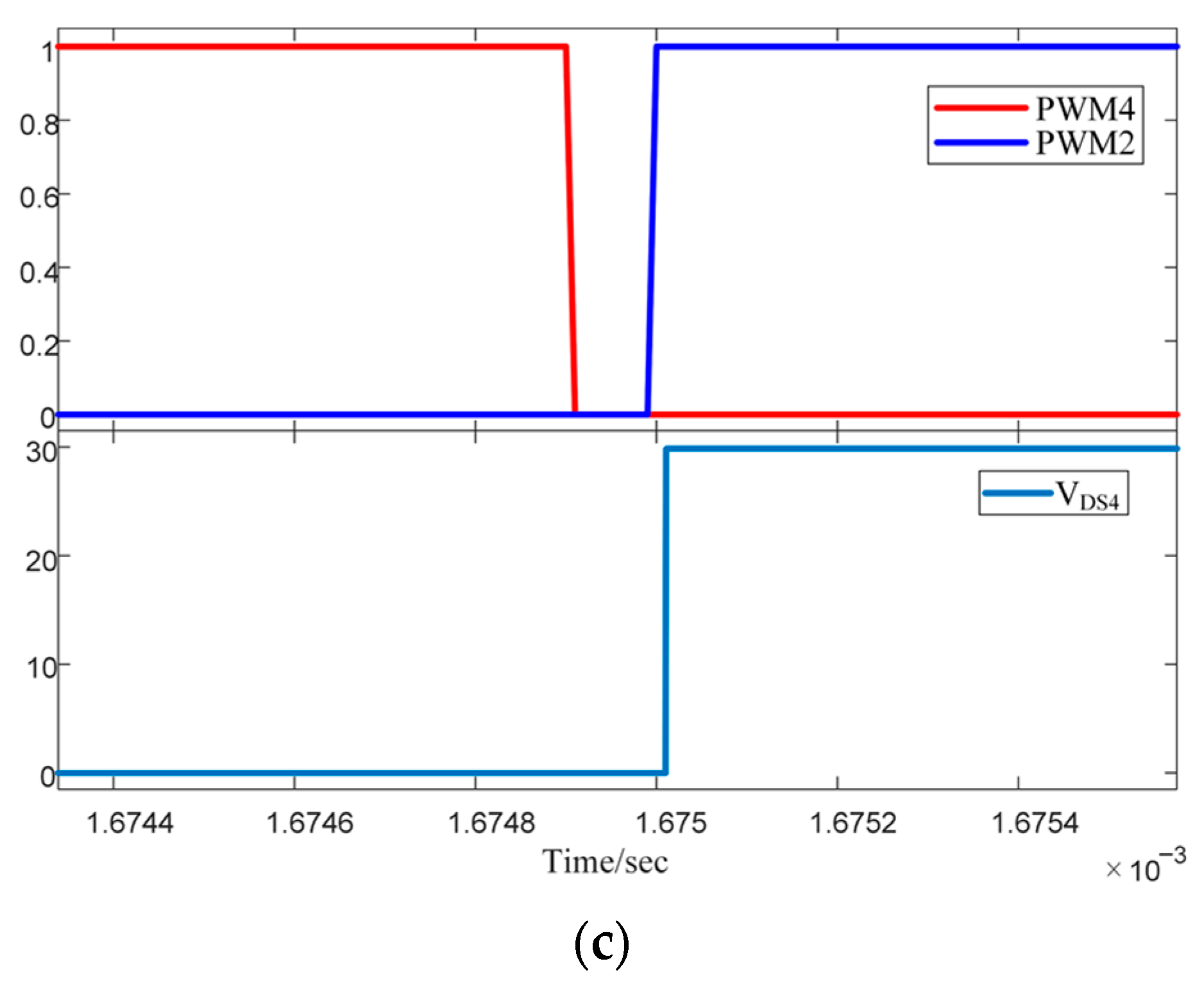
Without the auxiliary current source network, the load voltage and current waveforms are shown in Figure 7a; the trigger signals PWM1, PWM3 of the switch Q1 and the drain-source voltage waveform are shown in Figure 7b; the trigger signals PWM2 and PWM4 of the switches Q2, Q4, and the drain-source voltage waveform of the switch Q4 are shown in Figure 7c.
As can be seen, when switch Q1 is turned off, its drain-source voltage gradually increases and rises to the power supply voltage VDC before Q3 is turned on, which can realize the soft turn-on of Q3. As for the switches Q2 and Q4, since the current has been commutated, the current cannot charge the capacitor when Q4 is turned off, and soft switching cannot be realized, which is consistent with the previous analysis. The output power is calculated as 23.59 W, and the efficiency is 98.6%, thus, the simulation and experiment are carried out at a low power level.
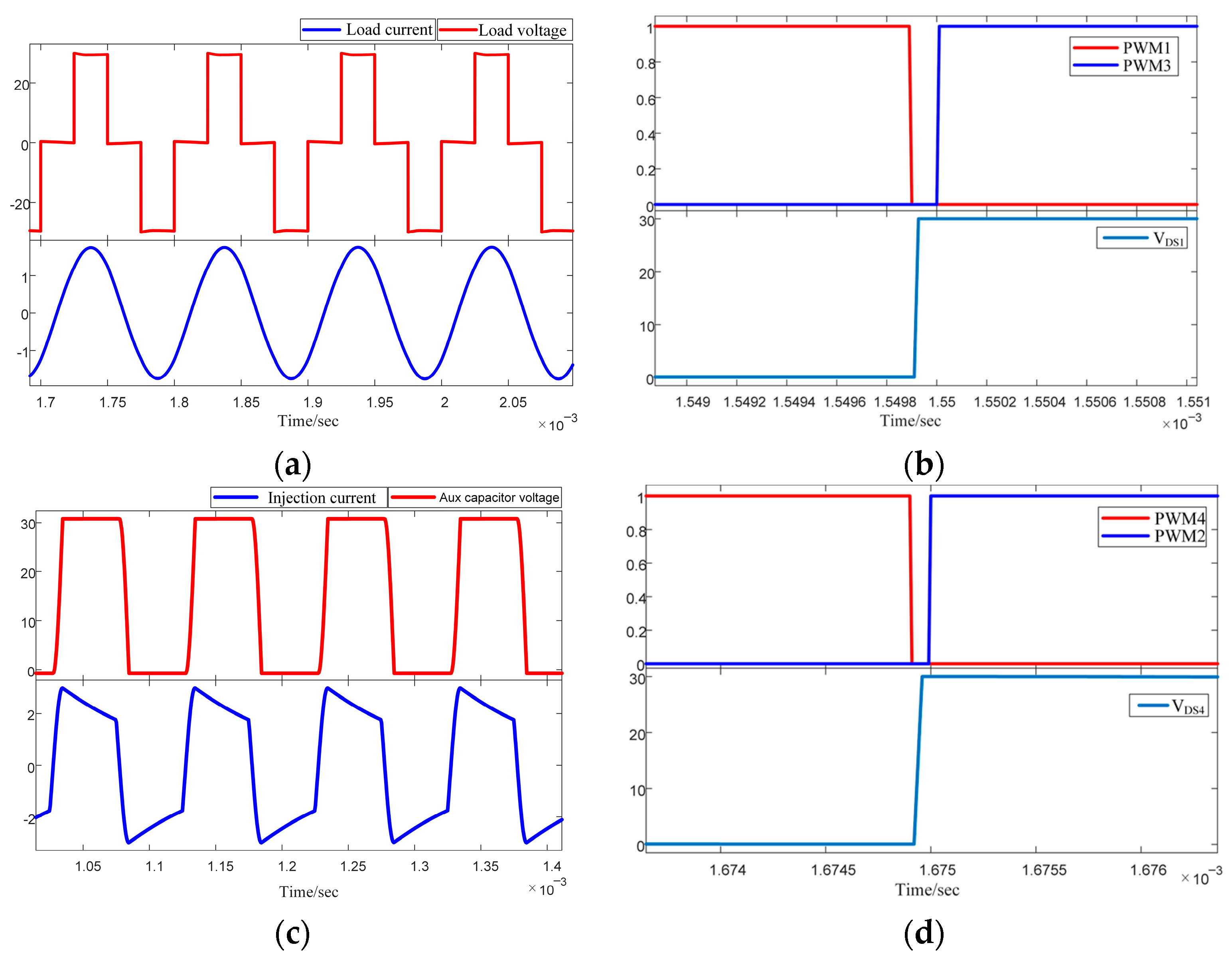
When connected to the auxiliary current source network, the load voltage and current waveforms are shown in Figure 8a; the trigger signals PWM1, PWM3 of the switch Q1, Q3, and the drain-source voltage waveform of the switch Q1 are shown in Figure 8b; the voltage waveform of the auxiliary capacitor and the current waveform injected by the current source is shown in Figure 8c; the trigger signals PWM2 and PWM4 of the switch Q2, Q4, and the drain-source voltage waveform of the switch Q4 are shown in Figure 8d.
As can be seen from the figure, since the auxiliary current source is connected, the commutated current is compensated by the injected current and charges the capacitor connected in parallel with the switches. Therefore, when Q4 is turned off, its drain-source voltage can increase, which creates conditions for soft turn-on of Q2. By using the auxiliary current source, the zero-voltage turn-on and turn-off of the four switches can be realized, which ensures the reliable operation of the switches. The voltage stress of the auxiliary capacitor is the voltage of the source, 30 V, the current stress of the auxiliary inductance is iLah, 3 A, which is in accordance with the previous analysis. The output power can be calculated as 23.33 W; however, the efficiency is 84.7%. It is the auxiliary current source that adds the source current, which leads to the input power rising and the efficiency decreasing.
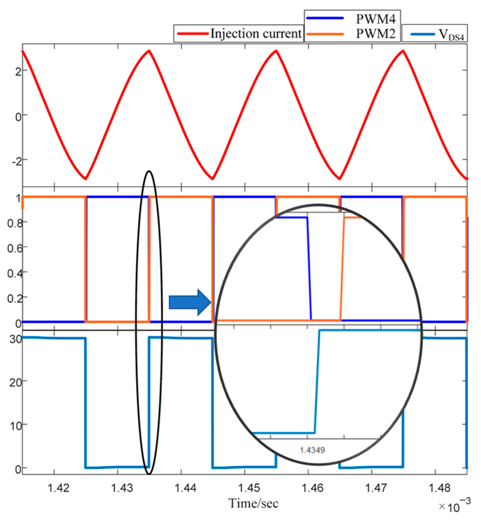
Since the leading bridge arm has been soft-switched by the load current, the following studies are related to the waveforms of the lagging bridge arm. When the switching frequency is increased to 50 kHz, the load capacitance working in the resonance state is calculated by (23) to be 10.13 nF, and the relevant waveforms of the injected current and the lagging bridge arm are shown in Figure 9.
As the frequency increases, the drop time tc of the injected current becomes shorter, and the drain-source voltage of the switch Q4 can be charged to the power supply voltage VDC before the switch Q2 conduction signal, realizing a soft switching of the lagging bridge arm.
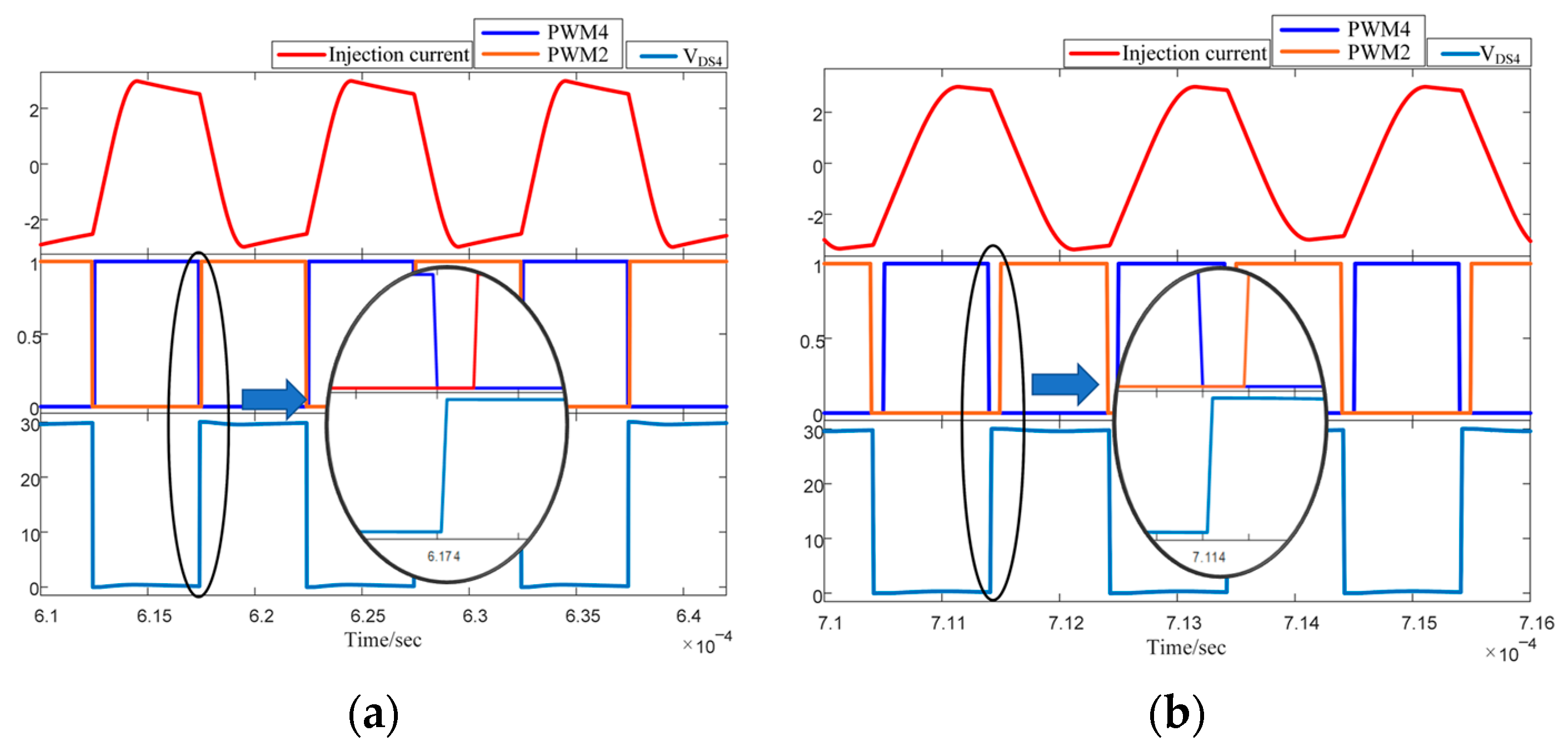
When the switching frequency is 100 kHz and 500 kHz, the injected current and the related waveforms of the lagging bridge arm are recorded, respectively, as shown in Figure 10.
By switching the network parameters of the auxiliary current source with different numbers, soft switching with a switch frequency range of 10 kHz–500 kHz can be realized.
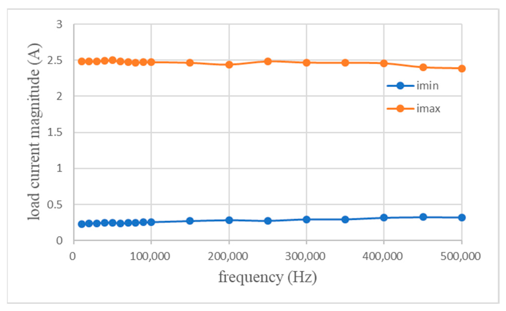
In order to determine the range of the phase shift angle corresponding to each frequency band, the range of the load current waveform magnitude when soft switching can be achieved at each frequency is now measured and recorded in Figure 11.
It can be seen from the figure that in the frequency range of 10 kHz–500 kHz, the magnitude of the load current that can achieve soft switching is 0.23 A–2.5 A, which is converted to a phase shift angle of 10°–170°, and that is consistent with the previous analysis.

3.3. Loss and Efficiency Analysis

The losses of the inverter mainly include losses of the switches and the auxiliary inductors. For losses of the full bridge switches, which can be distributed in turn-on losses, turn-off losses and conduction losses. In the proposed inverter, ZVS operation has been achieved in all four switches, the losses of the turn-on and the turn-off are insignificant and can be eliminated [19]. The conduction losses of the full bridge switches can be calculated according to (30):
P l o s s _ f b c o n = 2 R f b _ o n ( I 2 13 R M S + I 2 24 R M S )
where Rfb_on is the ON-state resistance of MOSFETs, I13RMS and I24RMS are the RMS current of the leading and lagging bridge, respectively.
There are only conduction losses for the bidirectional switches, which can be calculated according to (31):
P l o s s _ b i c o n = 2 R b i _ o n I 2 l a R M S
where Rbi_on is the ON-state resistance of the bidirectional switches, IlaRMS is the RMS current of the injected current.
For the losses of the auxiliary inductors, which can be derived by (32):
P l o s s _ i n d = I 2 l a R M S R L a
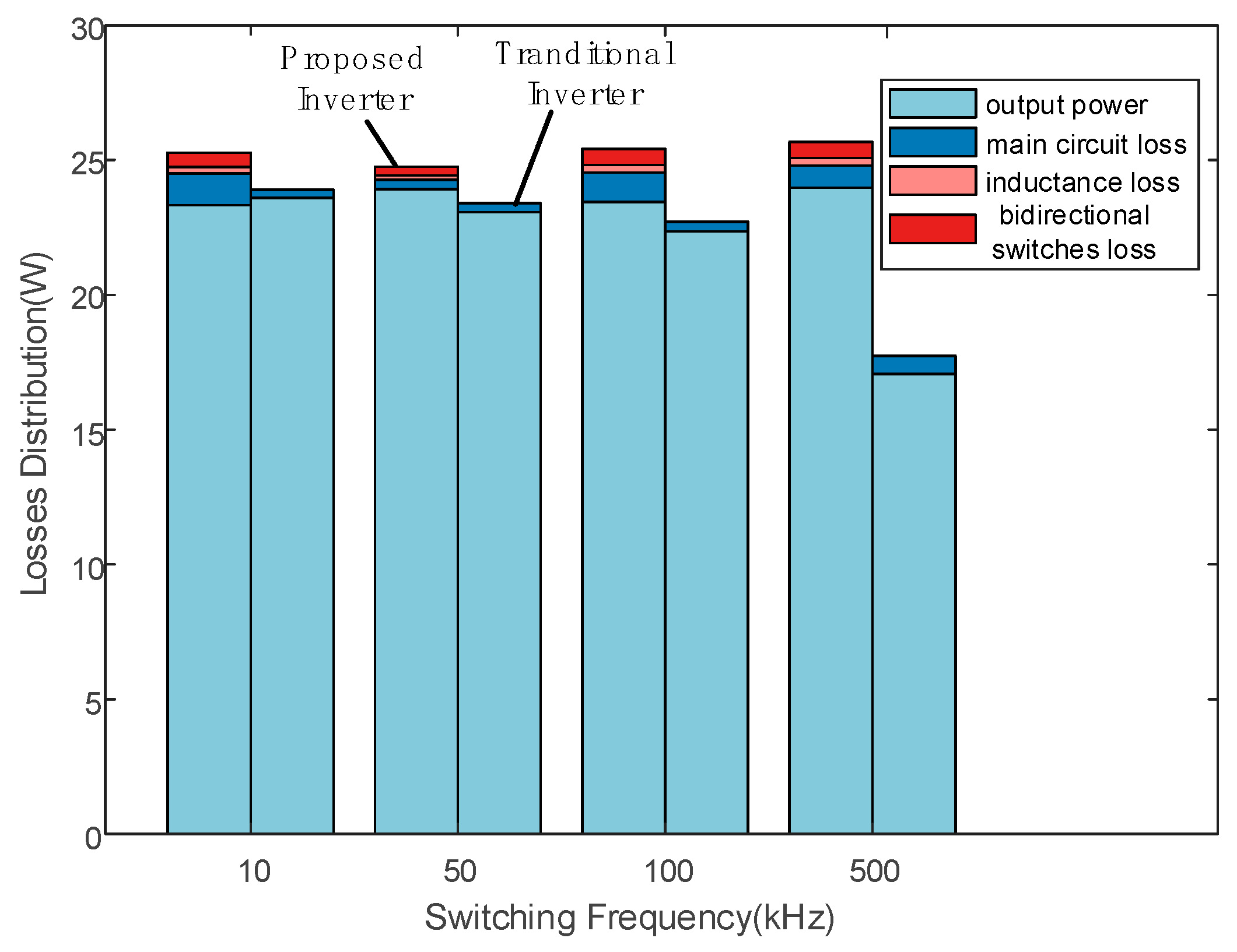
where RLa is the ESR of the auxiliary inductor. The power loss analysis is conducted, as shown in Figure 12.
It can be seen from Figure 12 that as the switching frequency increases, the output power of the traditional inverter decreases. In the proposed inverter, because of the injection current, the losses of the main circuit switches are larger than that in the traditional inverter. Although the loss of the proposed inverter is large, the output power does not change significantly with the increase of frequency and remains at a high level.
The efficiency of the inverter can be calculated as the ratio between its output to input power:
η = P o P i n = P o P o + P l o s s s e s
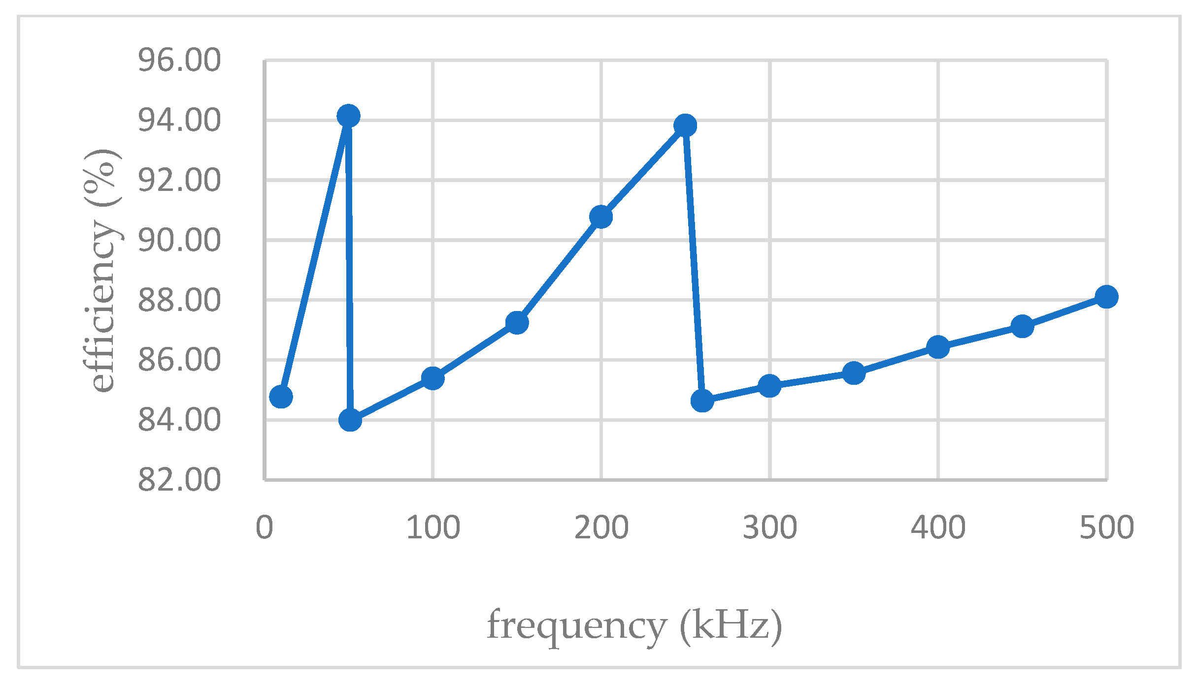
Based on the above analysis, the efficiency of the inverter at different frequency can be drawn and is indicated in Figure 13.
With the frequency increases, the efficiency of the inverter increases within the corresponding region and decreases to about 84% at the critical frequency. The maximum efficiency can reach 94.14% from Figure 13. In each frequency range, with the increase of frequency, the time of current flowing through the auxiliary circuit elements decreases, and the loss decreases accordingly, the frequency will increase. When switching the number of the auxiliary circuit, the frequency is the lowest frequency of the group, so the time of current flowing is prolonged, resulting in reduced efficiency. Although the efficiency is reduced, the soft switching in a wide frequency domain can be realized, the electrical stress of the MOSFETS is reduced, and larger output power can be achieved.

3.4. Scalability to High Power Application

In order to study the scalability of the proposed architecture to large size high voltage converter, only the input voltage is increased to 400 V, and other conditions remain unchanged.
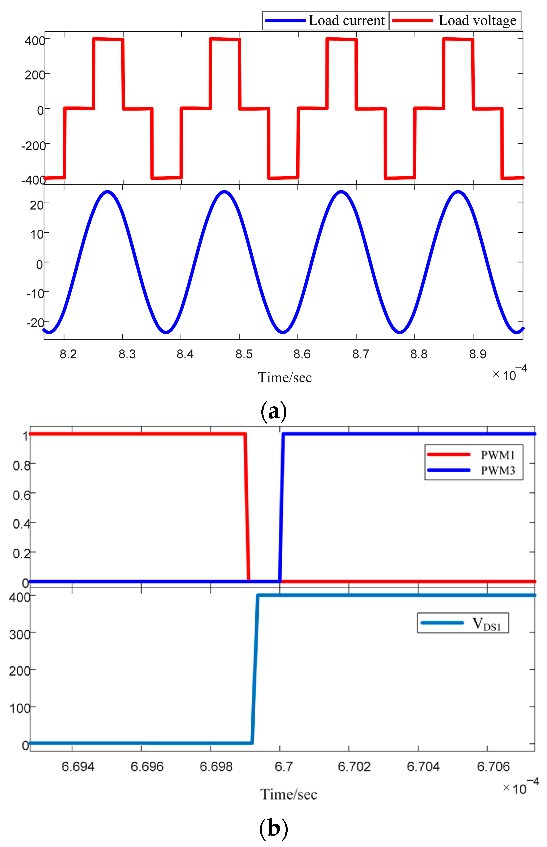
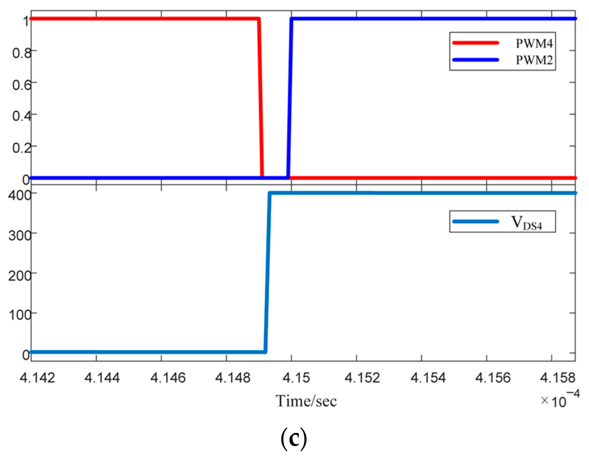
Taking the frequency of 50 kHz as an example, the load voltage and current waveforms are shown in Figure 14a; the trigger signals PWM1, PWM3 of the switch Q1, Q3, and the drain-source voltage waveform of the switch Q1 are shown in Figure 14b; the trigger signals PWM2 and PWM4 of the switch Q2, Q4, and the drain-source voltage waveform of the switch Q4 are shown in Figure 14c.
It is obvious that the proposed inverter can still achieve soft switching under high power level, and the output power is 4.25 kW, the efficiency is 94.9%, which proves the scalability of the architecture.

4. Experimental Results and Analysis

To verify the ability of the proposed circuit to achieve soft switching within a certain frequency range, an experimental circuit board is now developed based on the circuit topology shown in Figure 6. Its parameters are shown in Table 2. In this experiment, due to the limitation of laboratory conditions, the power level is not high, and efficiency is not the primary consideration. According to the different switching frequencies, the network parameters of each auxiliary current source are selected according to Table 1.

4.1. Without Auxiliary Current Source

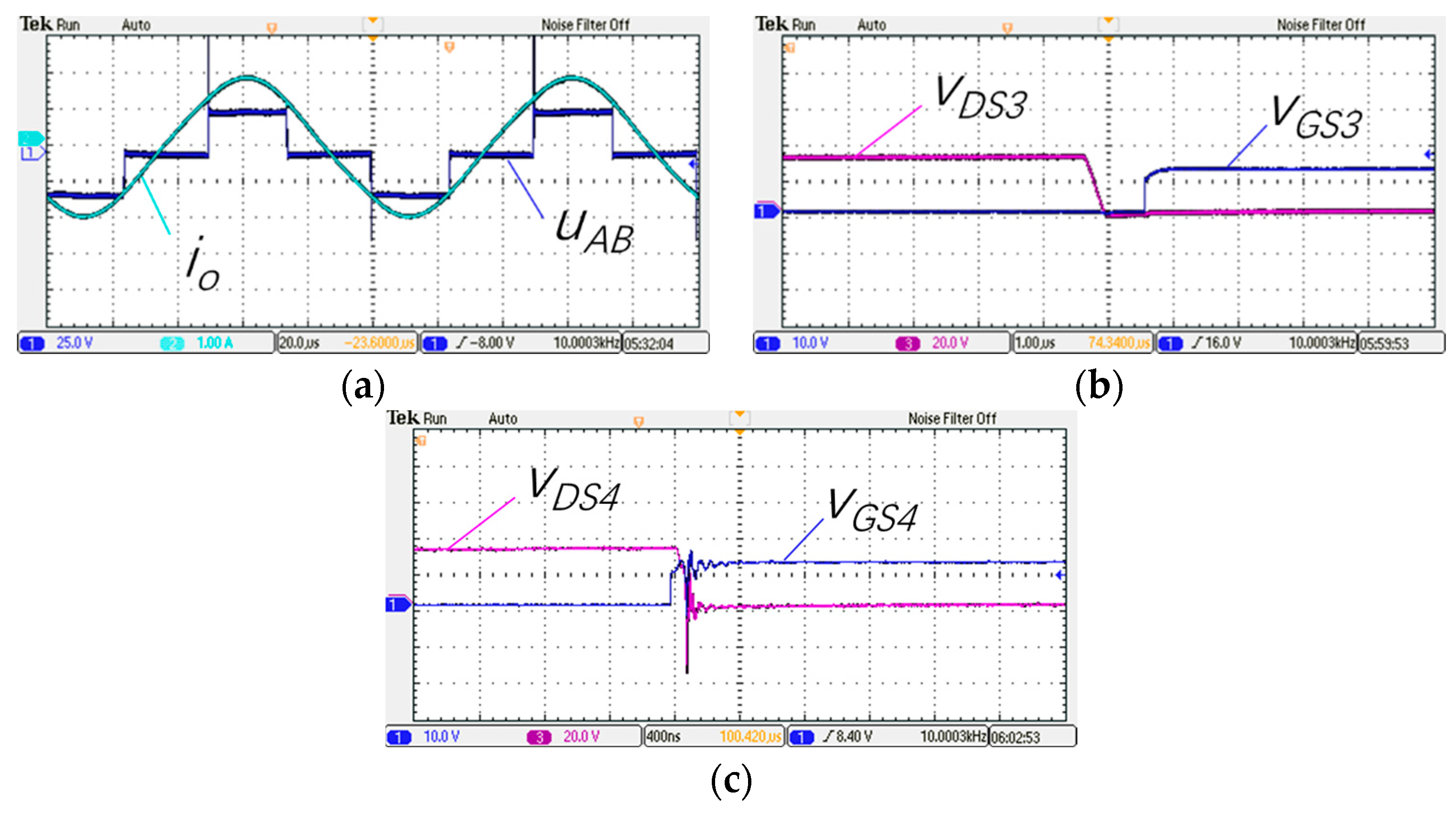
Without the auxiliary current source, the load voltage and current, and the related waveforms of the leading and lagging bridge arms of the basic PSFB topology at a switching frequency of 10 kHz are measured, as shown in Figure 15. It can be seen that when the load inductance and the load capacitor resonate in series, the drain-source voltage vds3 of the leading bridge arm switch Q3 has dropped to zero before the turn-on signal, indicating that the leading bridge arm can achieve zero-voltage soft switching. However, the lagging bridge arm switch Q4 cannot discharge its parallel capacitor C4 due to the reverse current, and its drain-source voltage vds4 has not yet dropped to zero when the turn-on signal comes, which leads to hard switching and the waveform of the load voltage shows an obvious overshoot.

4.2. With Auxiliary Current Source

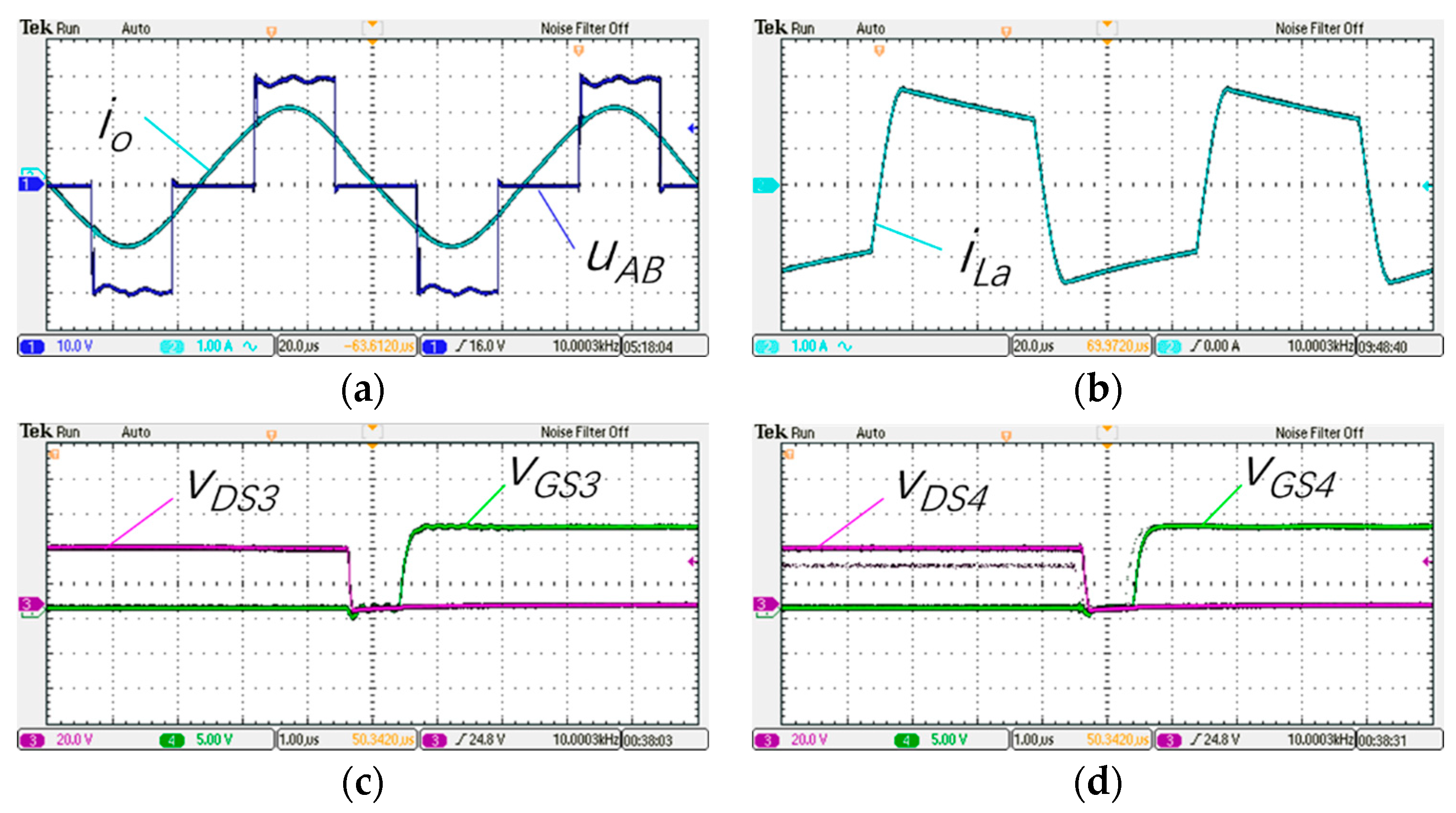
With the auxiliary current source, the load voltage and current, the current injected by the auxiliary current source, and the related waveforms of the leading and lagging bridge arms at 10 kHz are measured, as shown in Figure 16.
It can be seen from the figure that the leading bridge arm can still achieve zero-voltage soft switching, and the drain-source voltage vds4 of the switch Q4 can be discharged when the turn-on signal comes, and is completely discharged before the turn-on signal, indicating that the lagging bridge arm can also achieve zero-voltage soft switching due to the auxiliary current source. The current stresses of the auxiliary inductance and the auxiliary capacitor are 2.56 A, 1.52 A, which are lower than their respective current ratings of 3 A, 2 A. Additionally, the voltage stresses of the auxiliary inductance and the auxiliary capacitor are both the voltage of the source, i.e., 30 V. Because of the addition of an auxiliary current source, the overshot of the load voltage is significantly alleviated.

4.3. Operation of the Broadband Auxiliary Current Source

Since the actual coil inductance has a higher equivalent series resistance at high frequency, the actual frequency range is selected as 10 kHz–200 kHz. In order to verify the soft switching capability of this topology in the 10 kHz–200 kHz broadband, the frequency of 50 kHz, 100 kHz and 200 kHz is selected as the test frequency points in this paper, and the relevant waveforms of the lagging bridge arm are measured to verify the capability of soft switching.
At each test frequency point, each auxiliary current source network is selected and the injected current at the corresponding operating frequency and the related waveforms of the lagging bridge arm are measured, and the results are shown in Figure 17, Figure 18 and Figure 19, respectively.
At each test frequency point, the selected auxiliary current source network parameters can ensure the zero-voltage soft switching of the lagging bridge arm at this frequency. By selecting each auxiliary current source network, zero-voltage soft-switching in the wide frequency range of 10 kHz–200 kHz can be realized.

5. Conclusions

In order to solve the problem of the current commutation in the lagging leg of full-bridge converter under broadband conditions, a current injection method is utilized in this paper, which can realize the function of soft switching of the lagging leg by injecting current into the lagging bridge arm. This paper analyses the influence of the injected current source on the circuit in different operating modes, gives the calculation method of the parameters of the auxiliary circuit adapted to different frequency ranges, analyses and discusses the influence of the auxiliary circuit on the power distribution of the converter. The feasibility of the scheme is verified by simulation and experiments. The results show that the load power can fully meet the requirements of soft switching in the frequency range from 10 kHz to 200 kHz.

Author Contributions

Conceptualization, investigation, supervision, project administration and funding acquisition, X.Z. and D.L.; resources, methodology, software and validation, Q.X. and Z.Z.; writing—original draft preparation, formal analysis and data curation, Y.Z. All authors have read and agreed to the published version of the manuscript.

Funding

This research received no external funding.

Conflicts of Interest

The authors declare no conflict of interest.

References

  1. Chudjuarjeen, S.; Sangswang, A.; Koompai, C. LLC resonant inverter for induction heating with asymmetrical voltage-cancellation control. In Proceedings of the 2009 IEEE International Symposium on Circuits and Systems (ISCAS), Taiwan, China, 24–27 May 2009; pp. 2874–2877. [Google Scholar]
  2. Wang, Q.; Wang, Y. Resonant DC link soft-switching inverter with low-loss auxiliary circuit. Int. J. Electron. 2019, 106, 1602–1615. [Google Scholar] [CrossRef]
  3. SFeng, X.; DianGuo, X.; YuXiu, L. A novel zero-voltage and zero-current-switching full-bridge PWM converter. In Proceedings of the IECON’03 29th Annual Conference of the IEEE Industrial Electronics Society (IEEE Cat. No. 03CH37468), Roanoke, VA, USA, 2–6 November 2003; pp. 383–390. [Google Scholar]
  4. Tabisz, W.; Jovanic, M.; Lee, F. High-frequency multi-resonant converter technology and its applications. In Proceedings of the 1990 Fourth International Conference on Power Electronics and Variable-Speed Drives (Conf. Publ. No. 324), London, UK, 17–19 July 1990; pp. 1–8. [Google Scholar]
  5. Lee, F.C. High-frequency quasi-resonant converter technologies. Proc. IEEE 1988, 76, 377–390. [Google Scholar] [CrossRef]
  6. Steigerwald, R.L. A comparison of half-bridge resonant converter topologies. IEEE Trans. Power Electron. 1988, 3, 174–182. [Google Scholar] [CrossRef]
  7. Cai, H.; Shi, L.; Li, Y. Harmonic-based phase-shifted control of inductively coupled power transfer. IEEE Trans. Power Electron. 2013, 29, 594–602. [Google Scholar] [CrossRef]
  8. Yao, C.; Dong, S.; Zhao, Y.; Zhou, Y.; Mi, Y.; Li, C. High-frequency composite pulse generator based on full-bridge inverter and soft switching for biological applications. IEEE Trans. Dielectr. Electr. Insul. 2016, 23, 2730–2737. [Google Scholar] [CrossRef]
  9. Bhaskar, D.V.; Vishwanathan, N. Full bridge series resonant inverter for induction cooking application. In Proceedings of the 2012 IEEE 5th India International Conference on Power Electronics (IICPE), Delhi, India, 6–8 December 2012; pp. 1–5. [Google Scholar]
  10. Mishima, T.; Takami, C.; Nakaoka, M. A new current phasor-controlled ZVS twin half-bridge high-frequency resonant inverter for induction heating. IEEE Trans. Ind. Electron. 2013, 61, 2531–2545. [Google Scholar] [CrossRef] [Green Version]
  11. Takami, C.; Mishima, T.; Nakaoka, M. A new ZVS phase shift-controlled class D full-bridge high-frequency resonant inverter for induction heating. In Proceedings of the 2012 15th International Conference on Electrical Machines and Systems (ICEMS), Sapporo, Japan, 21–24 October 2012; pp. 1–6. [Google Scholar]
  12. Salvi, B.; Porpandiselvi, S.; Vishwanathan, N. A Three Switch Resonant Inverter for Multiple Load Induction Heating Applications. IEEE Trans. Power Electron. 2022, 37, 12108–12117. [Google Scholar] [CrossRef]
  13. Kim, J.-W.; Lee, M.; Lai, J.-S. A new control method for series resonant inverter with inherently phase-locked coil current with induction cookware applications. In Proceedings of the 2018 IEEE Applied Power Electronics Conference and Exposition (APEC), San Antonio, TX, USA, 4–8 March 2018; pp. 3517–3522. [Google Scholar]
  14. Herasymenko, P.; Yurchenko, O. An Extended Pulse-Density-Modulated Series-Resonant Inverter for Induction Heating Applications. In Proceedings of the 2020 IEEE 61th International Scientific Conference on Power and Electrical Engineering of Riga Technical University (RTUCON), Riga, Latvia, 5–7 November 2020; pp. 1–8. [Google Scholar]
  15. Leyh, G.; Kennan, M. Efficient wireless transmission of power using resonators with coupled electric fields. In Proceedings of the 2008 40th North American Power Symposium, Calgary, AB, Canada, 28–30 September 2008; pp. 1–4. [Google Scholar]
  16. Doan, V.D.; Jeng, J.T.; Tsao, T.H.; Pham, T.T.; Huang, G.W.; Dinh, C.H.; Lee, T.H.; Mei, P.I. Development of a Broad Bandwidth Helmholtz Coil for Biomagnetic Application. IEEE Trans. Magn. 2021, 57, 1–5. [Google Scholar] [CrossRef]
  17. Ruan, X.; Yan, Y. An improved phase-shifted zero-voltage and zero-current switching PWM converter. In Proceedings of the APEC’98 Thirteenth Annual Applied Power Electronics Conference and Exposition, Anaheim, CA, USA, 15–19 February 1998; pp. 811–815. [Google Scholar]
  18. Xiao, Q.; Zhao, J.; Wang, M. Research on frequency tracking capacitive PWM of induction heating power supply. In Proceedings of the 2010 International Conference on Challenges in Environmental Science and Computer Engineering, Wuhan, China, 6–7 March 2010; pp. 377–380. [Google Scholar]
  19. Chen, G.; Zhou, Y.; Ding, Z.; Zeng, J.; Huang, L. A Three-Leg-Based Full-Bridge Converter with Wide Input Voltage Range. IEEE Trans. Ind. Electron. 2021, 69, 5690–5699. [Google Scholar] [CrossRef]
Figure 1. Diagram of Full bridge inverter structure.
Energies 15 08661 g001
Figure 2. Phase-shift control signal and load voltage and current waveforms.
Energies 15 08661 g002
Figure 3. Main waveforms of the auxiliary current source network.
Energies 15 08661 g003
Figure 4. Current path diagrams for various switching modes. (af) Switching mode 1–6.
Energies 15 08661 g004
Figure 5. Relationship between frequency and auxiliary inductance.
Energies 15 08661 g005
Figure 6. Simulation circuit model. (a) Main circuit diagram; (b) Auxiliary current source network.
Energies 15 08661 g006
Figure 7. Main waveforms without auxiliary current source. (a) Load voltage and current waveform; (b) Q1Q3 trigger signal and Q1 drain-source voltage waveform; (c) Q2Q4 trigger signal and Q4 drain-source voltage waveform.
Energies 15 08661 g007aEnergies 15 08661 g007b
Figure 8. Main waveforms with auxiliary current source. (a) Load voltage and current waveform; (b) Q1Q3 trigger signal and Q1 drain-source voltage waveform; (c) Voltage waveform of the auxiliary capacitor and the auxiliary current source injection current waveform; (d) Q2Q4 trigger signal and Q4 drain-source voltage waveform.
Energies 15 08661 g008
Figure 9. The main waveforms of the injected current and lagging bridge arm at 50 kHz with auxiliary current source.
Energies 15 08661 g009
Figure 10. The main waveforms of the injected current and lagging bridge arm at 100 kHz and 500 kHz. (a) The main waveforms of the lagging bridge arm and the injected current at 100 kHz; (b) The main waveforms of the lagging bridge arm and the injected current at 500 kHz.
Energies 15 08661 g010
Figure 11. Range of load current amplitudes for soft switching at each frequency.
Energies 15 08661 g011
Figure 12. Comparison of power distribution in different frequencies.
Energies 15 08661 g012
Figure 13. The efficiency of the inverter with variation in frequency.
Energies 15 08661 g013
Figure 14. Main waveforms of the inverter under high power level. (a) Load voltage and current waveform; (b) Q1Q3 trigger signal and Q1 drain-source voltage waveform; (c) Q2Q4 trigger signal and Q4 drain-source voltage waveform.
Energies 15 08661 g014aEnergies 15 08661 g014b
Figure 15. The relevant waveforms without auxiliary current source. (a) Load voltage and current waveforms; (b) Q3 trigger signal and Q3 drain-source voltage waveform; (c) Q4 trigger signal and Q4 drain-source voltage waveform.
Energies 15 08661 g015
Figure 16. The relevant waveforms with auxiliary current source. (a) Load voltage and current waveforms; (b) Injection current waveform; (c) Q3 trigger signal and Q3 drain-source voltage waveform; (d) Q4 trigger signal and Q4 drain-source voltage waveform.
Energies 15 08661 g016
Figure 17. Injection current and lagging bridge arm waveform at 50 kHz. (a) Injection current; (b) Related waveform.
Energies 15 08661 g017
Figure 18. Injection current and lagging bridge arm waveform at 100 kHz. (a) Injection current; (b) Related waveform.
Energies 15 08661 g018
Figure 19. Injection current and lagging bridge arm waveform at 200 kHz. (a) Injection current; (b) Related waveform.
Energies 15 08661 g019
Table 1. Auxiliary current source parameters and corresponding frequency ranges.
NumberLa (μH)Ca (nF)Lowest Frequency fL (kHz)Highest Frequency fH (kHz)
144.18220.99.9950.80
28.6943.4750.80257.66
32.7813.9158.78803.94
Table 2. Circuit component parameters.
ParameterValue
power supply voltage VDC (V)30
Phase shift angle θ (°)90
Load inductance L (mH)1
Load Resistance R (Ω)15
Gate Signal Duty Cycle D (%)50
MOSFETNCE8290AC
Bidirectional switchAOD482
ESR of the inductance La1 (mΩ)150
ESR of the inductance La2 (mΩ)55
ESR of the inductance La3 (mΩ)35
Auxiliary diodeSS510
Gate driver chipUCC27712
Publisher’s Note: MDPI stays neutral with regard to jurisdictional claims in published maps and institutional affiliations.