1. Introduction
Due to the ever-increasing installed capacity of photovoltaics (PV) and wind power, new energy penetration is gradually increasing, especially for PV systems. The compound annual growth rate of PV over the last decade has exceeded 40%, and it has become one of the fastest growing renewable energy generation technologies [
1,
2]. The proportion of PV power generation in global electricity production will be a further breakthrough. Moreover, PV systems are extensively applied to the DC side of converters in the future.
The new energy uses a power electronic converter as the grid-connected interface. The traditional voltage-source or current-source inverters can only realize boost or buck; thus, they cannot achieve wide-range output voltage. Meanwhile, the upper and lower legs of traditional inverters cannot be switched on simultaneously, which affects its reliability. Z-source (ZS) and quasi-Z-source (qZS) inverters have been broadly investigated because they are able to deal with the problems in traditional inverters. Conventionally, PV and other DC power should be connected to the inverter through an intermediate bidirectional converter, which requires more power electronic elements, additional conversion stage, and increased power losses [
3]. ZS and qZS inverters have their unique structure that can realize both buck or boost features without any extra component in the circuit, resulting in a cheap and less sizable solution [
4]. However, ZSI is usually connected to the grid through the
LCL filter, which has characteristics of a third-order system [
5]. This causes an amplitude peak at the resonant frequency and phase variation, leading to the output oscillation and increasing the difficulty of the control system design.
Grid-connected inverters without isolation transformers have the merits of small size, high efficiency, and low cost, becoming more attractive. However, they are unable to suppress DC injection automatically, resulting in poor power quality and excessive heat and loss. Hence, the international standard for the dc current injection of the grid-connected inverter has been formulated, limited to less than 0.5% of the rated current [
6]. The main causes of the DC component in grid-connected inverters without isolated transformers are zero drift and detection error of the sensor, inconsistent saturation voltage drop between upper and lower switches of the same leg under pulse width modulation (PWM), asymmetry of gate drive pulse, etc. [
7]. At present, much research has been conducted on the DC component suppression inside. The main methods include the inverter topology method, detection compensation method, capacitor blocking method, intelligent control method and other solutions. Reference [
8] proposed a single-phase half-bridge inverter topology with DC component suppression, but it has a small capacity and is only suitable for low-power applications. Reference [
9] proposed an improved single-phase three-level diode clamped inverter, which overcame the disadvantages in reference [
8] and also improved the ability to suppress the DC component. The character of DC mitigation behavior of the capacitor can play an ‘open circuit’ role in the DC component. Thus, references [
10,
11] inserted the physical capacitor or virtual capacitor into the grid-connected inverter side to replace the transformer to suppress the DC component. However, this method makes the system unable to work in an ideal state and cannot fundamentally compensate for the DC component of the output voltage. References [
12,
13] used hardware to detect the DC component of the inverter output current. Based on the conventional grid-connected control method, they added a newly designed DC component compensation controller to adjust the reference signal or modulation signal to realize the compensation so as to suppress the DC component, but it requires higher detection methods and accuracy. Except for the hardware to extract the DC component, reference [
14] proposed software technology of a sliding window double-iteration method to obtain a DC component and to utilize an adaptive back-propagation (ABP) neural network to adjust the coefficient of the PID controller online to minimize the DC component injection, but it requires complex algorithms and needs high-speed microprocessors for data storage and calculation. The other solutions designed in Reference [
15] were an accurate sensor that can measure milliamperes of dc current mixed in more than 10 A of ac current; thus, the DC component can be suppressed below the standard limit of 5 mA. However, the design of this accurate sensor is complex and costly. Another solution in reference [
16] used a proportional integral resonant (PIR) controller to realize high gain in low frequency to mitigate the DC component caused by the grid voltage measurement errors and disturbances. Then, the DC component arising from the grid current measurement errors was extracted by a second-order low pass filter, which was utilized for dc suppression compensation. This solution requires a difficult design of the PIR controller and a high accuracy of sensors.
Considering the disadvantages of the existing DC component suppression methods and complicated design of the LCL grid-connected filter third-order system, this paper proposes a novel DC component suppression strategy for grid-connected ZSI based on the split capacitor method of DOB.
The main contributions of this paper are summarized as follows:
- (1)
The problems of resonance and the DC component in a grid-connected ZSI are analyzed, and the control strategy of a grid-connected ZSI is established.
- (2)
A split capacitor method is researched in detail to eliminate resonance problems and to increase low-frequency gain and crossing frequency of the system; thus, the system performance is improved.
- (3)
The basic principle of DOB is presented in detail, and the DC component suppression strategy based on DOB is proposed. The stability analysis of the proposed strategy is proven, and the effectiveness is verified by various comparison results of the simulation and experiment.
This paper is organized as follows:
Section 1 introduces the causes of the DC component and the existing dc current injection suppression strategy for the grid-connected inverter.
Section 2 builds the grid-connected ZSI system and its control strategy.
Section 3 describes the split capacitor method in detail.
Section 4 analyzes the disturbance suppressing effect with and without the proposed DOB, and the stability analysis of it is demonstrated. The simulated and experimental results are presented in
Section 5.
2. System Topology Model
ZSI is a new inverter topology. The inverter is coupled with a DC source by using the Z-source network composed of inductance and capacitance so that the upper and lower legs of inverter can shoot through. By inserting the shoot through the zero vector in the modulation and by changing the voltage gain, the step up or step down can be realized, achieving the wide-range output voltage. It effectively overcomes the disadvantages of the traditional voltage source and current source inverter [
17].
Figure 1 shows the topology of ZSI, including DC power, Z-source single-phase full-bridge inverter,
LCL filter, etc. The DC power supply of ZSI is different from the traditional inverter, which can be either a voltage source or a current source. It can be a battery, fuel cell stack, PV system, capacitor or a combination of them.
,
,
,
are the capacitor and inductor of the Z-source network;
,
,
are the capacitor and inductor of the
LCL filter;
is the Z-source capacitor voltage;
UAB is the voltage between the middle points A and B of the inverter full bridge, i.e., the output voltage of the inverter switch side;
is grid voltage;
iL is the inductance current of the Z-source network;
if is the grid current.
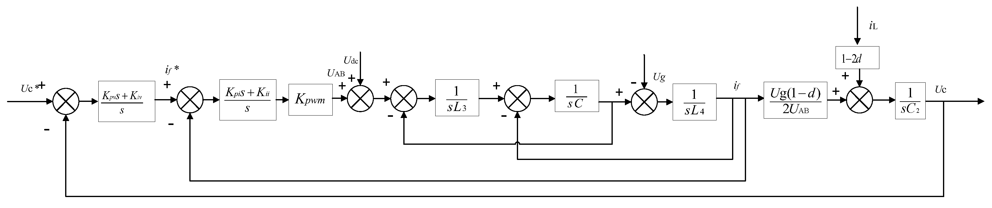
System Closed-Loop Control Scheme
The grid-connected control system of ZSI adopts a voltage and current double closed-loop control, i.e., the inner loop of the grid-connected current and the outer loop of the Z-source capacitor voltage. Since there is a certain relationship between the Z-source capacitor voltage and the inverter dc-link voltage, controlling the Z-source capacitor voltage can stabilize the inverter dc-link voltage [
18]. As shown in
Figure 1, the output amplitude of the Z-source capacitor voltage outer loop regulator is given as the input amplitude of current inner loop. The input amplitude is synchronized with the grid voltage through the phase-locked loop (PLL) to obtain the current inner loop reference signal. This reference signal is compared with the feedback grid current, and the current regulator adjusts the PWM modulation signal to drive the inverter S1~S4 switch tube. The overall control block diagram is shown in
Figure 2.
Udc is equivalent to the DC disturbance component; d is the shoot-through duty; Kpwm is the PWM inverter gain coefficient; Kpi, Kii are the proportional gain and integral gain of the grid side current control loop, respectively; Kpv, Kiv are the proportional gain and integral gain of the capacitance voltage control loop, respectively.
Figure 3 and
Figure 4 show the design of the inner and outer control loop for a grid-connected ZSI.
3. Split Capacitor Method
The
LCL filter is used to filter the high-frequency harmonics caused by the PWM switch, which has a great filtering effect. However, the
LCL filter is a third-order system, which has an amplitude peak at a resonant frequency, resulting in a phase sharp change, affecting system stability, and increasing the difficulty of the control system design. By using the split capacitor method to select the appropriate inductance–capacitance ratio, the third-order
LCL filter system turns into a first-order one [
19].
Figure 5 is the traditional grid-side current feedback control. According to
Figure 5, the transfer function from the grid-side current
i2 to inverter output voltage
UAB and the feedback control system loop gain can be derived as:
L is the total inductance of the filter, and , ;
According to the split capacitor method, the middle bypass capacitor
C of the
LCL filter is split into the front and rear parts
C1 and
C2 (
,
) in parallel. Afterward, the middle current
is taken as the feedback control, as shown in
Figure 6.
The transfer function of the inverter output voltage
to feedback current
can be expressed as:
When
, Formula (3) can simplify a third-order system to first-order, as shown in Formula (4). In addition, the feedback control system loop gain can also be simplified as Formula (5):
is the simplified condition. It can be represented by inductance and capacitance:
The bode plot of the current control open loop transfer functions with and without the split capacitor method can be drawn using the parameters in
Table 1. As shown in
Figure 7, without the split capacitor method, the original control system has a resonant peak at the resonant frequency, and the phase offset is close to 180°. Hence, the control system loop gain at the filter resonant frequency should be within 0 dB, which requires the proportional gain of the
regulator to be reduced. The low-frequency gain and crossover frequency of the system also decrease, which makes the disturbance and harmonic suppression ability low. The system is prone to instability. When adopting the split capacitor method, there is no resonance in the system. The
controller is no longer limited, which can design a larger proportional gain. Compared with the original system, the low-frequency gain is significantly increased, and the crossing frequency is improved, which improves the performance of the system.
In
Figure 8,
Udc is equivalent to the DC disturbance component. The DC offset of the inverter output is hypothetically generated by the equivalent DC disturbance component
Udc. The transfer function of the DC disturbance component
Udc to output current
if is:
is the total inductance of the filter simplified by the split capacitor method.
4. DC Component Suppression Based on a Disturbance Observer
Before proposing the strategy of DOB to suppress the DC component, the basic principle of DOB is analyzed, and the basic model of DOB is established, which provides a basis for suppressing the DC component of the grid-connected inverter.
4.1. Basic Principle of the Disturbance Observer
The basic principle of the disturbance observer [
20,
21] is shown in
Figure 9.
is the actual controlled object,
is the nominal model,
is the controller,
and
are the input and output of the system, respectively,
is the intermediate operation variable, and
is the low-pass filter. Its principle is that the external disturbance of the controlled object and the difference between the actual output model and the nominal model caused by the change in model parameters is regarded as system disturbance
. Through the DOB, the disturbance estimation
is fed back to the controller output
immediately and accurately; thus, the system disturbance
can be eliminated in time before feedback.
From
Figure 9, in a system without DOB, the system output can be expressed as:
is the transfer function from input to output; is the transfer function from disturbance to output.
When a system employs DOB, the system output is:
is the transfer function from input to output; is the transfer function from disturbance to output.
Compared with (8) and (9), if the model is accurate, that is, if and = exist, it indicates that DOB can maintain a nominal system. For =, in the low and middle frequency, , the disturbance relative to output gain is zero, explaining that DOB can completely suppress the influence of disturbance on the output; at high frequency, , =, meaning that the DOB has no effect on the system at high frequency. Therefore, the designed low-pass filter can meet the demands.
4.2. Proposed Suppressed DC Component with the Disturbance Observer
The control block diagram of the current control loop system of the split capacitor method with DOB is shown in
Figure 10.
From
Figure 10, the transfer function from the DC disturbance component
Udc to output current
is:
In the DOB design, the relative order of
must be greater than or equal to the relative order of
[
22]. In this paper, the controlled object is a first-order system; thus, the
is designed as a first-order low-pass filter in (11).
is the filter time constant, and is the cut-off frequency. In order to improve the ability of the system to suppress the disturbance, the cut-off frequency should be as small as possible and higher than the harmonic frequency in the voltage signal. Here, .
Based on Formulas (7) and (10), the amplitude–frequency Bode diagram of the equivalent DC disturbance component to system output with and without a DOB can be derived, as shown in
Figure 11.
From
Figure 11, in the low-frequency range, when the DOB suppresses the DC disturbance component, the attenuation multiple of the DC disturbance component to the system output is significantly greater than that without the DOB. Furthermore, when the DOB exists, the lower the frequency is, the more obvious the attenuation of the DC disturbance component. Therefore, the DC component of the output current can be effectively suppressed by using a DOB so as to successfully mitigate the influence of the DC disturbance component on system output.
4.3. Stability Analysis of the System with the Proposed Scheme
In the proposed scheme, introducing the DOB may cause instability of the system. Hence, the stability of the system should be analyzed.
Figure 10 shows the block diagram of the system based on DOB. From
Figure 10, the open and closed loop transfer function of the system is given by (12) and (13), respectively:
In order to ensure the stability of the system, it must ensure that all the roots of (12) are located on the left-side of s-plane. The characteristic equation of the closed loop transfer function with the data of
Table 1 is expressed as:
According to (14), the Rouse criterion table is listed, as shown in (15).
From Formula (14) and (15), the coefficients of the characteristic equation of the closed loop transfer function and the elements in the Routh criterion table are all greater than zero. According to the Routh stability criterion [
23], the roots of the system are all located on the left-side of the s-plane, which means that the system is stable.
5. Simulation and Experiment Verification Results
The simulation model of the ZSI grid-connected system was built by Matlab/Simulink software to analyze the influence of a DC disturbance component on output current, and the proposed DOB suppression strategy in this paper is simulated and analyzed. The topology of ZSI is shown in
Figure 1, and the simulation parameters are shown in
Table 1.
Table 1.
Simulation Parameters.
Table 1.
Simulation Parameters.
| Parameter | Symbol | Value |
|---|
| DC source | Vdc | 500 V |
| Z-source capacitor | C1/C2 | 1000 μF |
| Z-source inductor | L1/L2 | 4 mH |
| Shoot-through duty | d | 0.2 |
| Filter inductor | L3/L4 | 2.5 mH |
| Filter capacitor | C3 | 12 μF |
| Total filter inductor | | 5 mH |
| Switch frequency | fs | 10 kHz |
Grid voltage/frequency
inverter gain coefficient | Ug/f
Kpwm | 220 V/50 Hz
380 |
| Current loop proportional gain | Kpi | 0.5 |
| Current loop integral gain | Kii | 0.05 |
| Voltage loop proportional gain | Kpv | 0.28 |
| Voltage loop integral gain | Kiv | 0.03 |
- A.
The ZSI grid-connected system operates normally
The grid-connected system operates without DOB, and the waveforms of the Z-source capacitor voltage and grid-connected current are shown in
Figure 12 and
Figure 13.
From
Figure 12,
Figure 13 and
Figure 14, in steady-state operation, the Z-source capacitor voltage can fluctuate around a constant DC voltage, and the fluctuation is small, which meets the requirements of voltage stabilization. The grid-side current can maintain the same phase operation with grid voltage, and the harmonic is small, indicating that the designed capacitor voltage outer loop and grid-side current inner loop control system can operate normally.
- B.
The comparison without an isolation transformer of the simulation results without and with the proposed DOB
Due to the ideal simulation conditions, the causes of the grid-connected inverter DC component in this paper will not be shown. In order to simulate the real situation, the DC disturbance component is added to the inverter output bridge arm to verify the effectiveness of the proposed DOB strategy. As shown in
Figure 15a, a 1.8% DC disturbance component is inserted, and Powergui FFT Analysis is used for analysis.
The proposed DOB is added to the simulation to verify the effectiveness of this scheme to suppress the DC component. As shown in
Figure 15b, the DC component of the grid-side current is suppressed to about 0.1% with DOB, which can basically eliminate the disturbance of the DC component and meet the 0.5% requirements of the grid-connected DC component.
- C.
The comparison results between the primary side and the secondary side of the isolation transformer
To verify the validity of the DC component suppression with the isolation transformer, ZSI is connected with the isolation transformer in
Figure 16. The current waveform and THD of the primary side and secondary side of the isolation transformer are compared, as shown in
Figure 17.
It can be seen from
Figure 17 that when the ZSI is connected with the isolation transformer, the DC component of the isolation transformer secondary side is almost zero, which means that the isolation transformer can isolate the DC component injected into the grid.
- D.
The comparison results with the isolation transformer and without the isolation transformer (with the DOB)
To demonstrate the effectiveness of the proposed DOB strategy in DC component suppression,
Figure 18 shows the comparison of the simulation results with the isolation transformer and without the isolation transformer (with the DOB).
Figure 18a shows that when ZSI is connected with the isolation transformer, there will be no DC component injected into the grid, resulting from the existence of the isolation transformer. Compared with
Figure 18b, the strategy proposed in this paper can suppress the DC component about 0.1% and meet the international standard of less than 0.5%. This means that the ZSI connected without the isolation transformer by DOB can achieve considerable DC component suppression results with the isolation transformer. Therefore, this strategy eliminates the need for the isolation transformer and serves the purpose of minimizing the cost and the complexity of the design.
- E.
Dynamic simulation of the proposed DOB strategy
To test the dynamic effect of the proposed DOB in a real process, the DOB is dynamically added in the simulation at 0.1 s, comparing the DC component of the output current before and after 0.1 s to verify its dynamic effect. The comparison results are shown in
Figure 19.
From
Figure 19a, when the DOB is not connected before 0.1 s, the DC component of the 0.08 s period is about 1.8%. As shown in
Figure 19b, when the DOB is connected at 0.1 s, the DC component of the output current is suppressed to about 0.1%, indicating that the DOB is effectively connected to the system at 0.1 s and that it suppressed the DC component of the output current.
- F.
Simulation of the proposed DOB strategy under distorted grid voltage
In order to simulate the worse operation condition that may occur in the power grid, the proposed DOB strategy was tested under distorted grid voltages containing fifth- and seventh-order harmonic components, with a 5% magnitude of the fundamental grid voltage, as represented in
Figure 20a.
Figure 20b shows the simulation results of THD of output current with the proposed DOB strategy under the grid condition in
Figure 20a. The simulation results show that the proposed DOB strategy can still work well when the grid voltage is perturbed by voltage distortion, reducing the DC component to less than 0.5% of the standard.
- G.
Comparisons with existing techniques
To further illustrate the performance of the proposed DOB strategy for suppressing the DC component, the proposed strategy is compared with the existing techniques. As aforementioned, the sliding window double-integration method was used to extract the DC component in [
14], and then, it utilized ABP-PID to suppress it. However, this technique cannot eliminate the dc bias by current feedback control caused in the current measurement error. The simulation results in [
14] show that the DC component decreases from 0.9 A to 78 mA, a total reduction of 91.03%, while the simulation results of the proposed DOB strategy are shown in
Figure 15, which decreases the DC component from 1.8% to 0.1%, a reduction of 94.4%; thus, the suppression effect is better.
Compared with the technique in [
16], the proposed DOB strategy uses a split capacitor to make the controller design simple and does not require an additional PIR controller in [
16] to increase the complexity of the control system. In this paper, the DOB is used to directly regard the DC component as an external disturbance, and no extra high-accuracy sensors are needed to detect the DC component; thus, it can also reduce the cost. From the suppression effect, the proposed DOB strategy in this paper can suppress the DC component at 0.1% lower than 0.24% in [
16].
- H.
Experimental results
The experimental platform uses the Modeling Tech StarSim MT6020 hardware to verify the above theory. The experimental parameters are shown in
Table 1, and the hardware equipment is shown in
Figure 21.
Figure 22 shows the grid-connected output current waveform and THD analysis of ZSI under normal operation. It can be seen that the output current contains about 1% of the DC component, which does not meet the DC component requirements of the grid-connected current.
Figure 23 shows the output current waveform and THD analysis when the proposed DC component suppression strategy based on DOB is employed. In this case, the DC component is suppressed to about 0.1%, implying that the proposed strategy in the experiment can effectively suppress the DC component of the output current to meet the requirements of the grid-connected DC component.


