Article

Design and Validation of a SEPIC-Based Novel Multi-Input DC-DC Converter for Grid-Independent Hybrid Electric Vehicles

by
Saikumar Bairabathina
and
Balamurugan S
*
School of Electrical Engineering, Vellore Institute of Technology, Vellore 632014, India
*
Author to whom correspondence should be addressed.
Energies 2022, 15(15), 5663; https://doi.org/10.3390/en15155663
Submission received: 7 July 2022 / Revised: 27 July 2022 / Accepted: 28 July 2022 / Published: 4 August 2022

Abstract

:
The multi-input converters play a significant role in developing grid-independent hybrid electric vehicles (GIHEVs). This article describes the design and analysis of a single-ended primary-inductor converter (SEPIC)-based novel multi-input DC-DC converter (MIC) for grid-independent hybrid electric vehicles (GIHEVs) that is powered by a solar photovoltaic (PV) panel and a fuel cell. The average large-signal, small-signal, and steady-state modelings are demonstrated to achieve high-quality design and analysis. The proposed converter promises wide output voltage and power flow management at lower duty cycle values. The sources can transfer energy to the load either jointly or individually in this converter with the appropriate operation of the power switches. A hardware prototype is also developed and tested efficiently to uphold the mathematical modeling, design, and operation. With fewer switches, lower voltage stress, and fewer circuit components, the suggested converter claims better gain and higher (96%) efficiency.

1. Introduction

To serve the increased electricity demand, both conventional and non-conventional sources are being overused [1,2,3]. Conventional energy sources are insufficient to meet excess electricity needs in the current context since they are rapidly decreasing [4,5,6]. Additionally, the combustion of fossil fuels to produce electricity has major environmental consequences, including climate change and poor air quality [7,8,9,10]. As a result, electricity production by non-conventional energy sources such as solar, wind, biomass, fuel cells, and many others is quickly expanding, notably in distributed generation [11,12,13,14,15,16]. However, the standalone usage of solar, wind, and other renewables is not suggested due to their highly varying nature [17,18,19,20]. As a result, there is a strong need to develop hybrid energy systems that use a variety of renewable energy sources to continually deliver power to the load [21,22,23,24].
The majority of electric vehicles (EVs) are battery-powered, which is determined by two factors: the current power system and lithium supplies [25,26,27,28,29]. As the number of BEVs grows, the strain on the existing power infrastructure grows, and the transportation industry, like crude oil now, may face a lithium shortage in one day [27,30]. To avoid the problems mentioned above, parallel research and development in fuel cell technologies, as well as fuel cell and solar cell integrated hybrid electric automobiles, should be conducted [31]. These cars are unaffected by the availability of lithium or the existing grid. In terms of energy and power density, hydrogen-based energy storage outperforms batteries [32,33,34]. According to the World Nuclear Association’s latest report, the usage of hydrogen has increased dramatically in recent years in a variety of applications [35]. Due to the high cost of hydrogen at the moment, it is preferable to use solar cells in conjunction with fuel cells to minimize hydrogen usage [36,37,38,39]. As illustrated in Figure 1, this grid-independent hybrid electric vehicle comprises a fuel cell, solar cell, MIC, and/or inverter, as well as an electric motor. In Figure 1, the MIC plays a critical role in determining system stability and performance [40,41,42,43]. Numerous MICs have been created, however, no converter is universally suitable for all applications [31,44,45,46,47]. The topology and design of each converter vary depending on the application, and each converter has its own set of advantages and limitations. For low- and medium-power GIHEVs, non-isolated MICs are more convenient than other types of MICs [31,48,49].
A new MIC topology that had been built using a basic single-ended primary-inductor converter (SEPIC) is discussed in [50]. It can be used to combine various sources, but at least one of them should always be a battery or energy storage system. On the other hand, the voltage stress on the semiconductor switches is high. In [51], a novel MIC configuration for integrating a battery with a super-capacitor for EVs is presented. In this converter, one input can energize the other input without the usage of external circuitry, and relays are employed to accomplish the desired operation, increasing the component count. The authors of [52] demonstrated the implementation of a super-boost MIC for solar-powered EVs. The converter had fewer components than [51], but the turn-on time of power switches remains high in order to attain higher voltage levels, resulting in increased losses. This converter is unable to provide electricity to both the load and the battery at the same time, therefore one source must always have a greater voltage than another. A novel bridge-type MIC for interconnecting different renewable energy systems is introduced in [53]. With the combination of unidirectional and bidirectional power electronic switches, it used fewer components and achieved high gain. There is a polarity difference between input and output voltages, and the number of switches functioning in each mode of operation increases the burden on each power semiconductor switch in the circuit. In [54], the authors presented a bidirectional MIC with critical inductance and voltage ripple calculations. This converter can perform bidirectional power transfer, but the number of power electronic switches is larger, and one of the inputs should be a battery. A multi-port MIC’s design and analysis are illustrated in [55]. The main objectives of this converter are to reduce component count and peak inverse voltage on the power switches. Unfortunately, the efficiency of this converter is low and, still, the number of components is very high. A modular non-isolated MIC with high gain and reduced voltage stress and component count is proposed in [56]. However, this converter has a high component count, and a few switches have higher voltage stress. Moreover, it has eight energy storage elements for the two-input circuit, and it is challenging to analyze the system and design a control logic. A non-isolated MIC with a non-coupled inductor is proposed for high gain and reduced component count for renewable energy applications in [57]. The component count is lower than in [55,56], but voltage stress is moderate, and the order of the system is still high. In addition, it is complicated to design a control logic for this converter.
Regardless of the fact that various types of MICs have been reported in the literature [31,45,46], a high-gain, high-efficiency, low-stress, and low-component MIC with the same input and output voltage polarity is required for GIHEVs to supply continuous power to the EV motor independently and simultaneously. The SEPIC has a higher gain, lower current consumption, less loss, higher efficiency, and lower overall harmonic distortion than traditional and advanced DC-DC converters [58,59]. There is no polarity difference between the input and output signals with this SEPIC converter. As a result, the suggested converter builds on the SEPIC converter concept to provide a new MIC for GIHEVs.
Section 2 of this study report delves into the operation and modeling of the designed fuel cell and solar photovoltaic panel-powered novel multi-input DC-DC converter for GIHEVs. We discuss the voltage stress and efficiency calculations for the suggested converter in Section 3, and we depict possible operating scenarios for the proposed converter in Section 4 to demonstrate the independent and simultaneous operation of sources. The experimental data are examined and discussed in Section 5. Finally, in Section 6, the conclusion and potential future research are outlined.

2. A SEPIC-Based Novel Multi-Input DC-DC Converter for Grid-Independent Hybrid Electric Vehicles

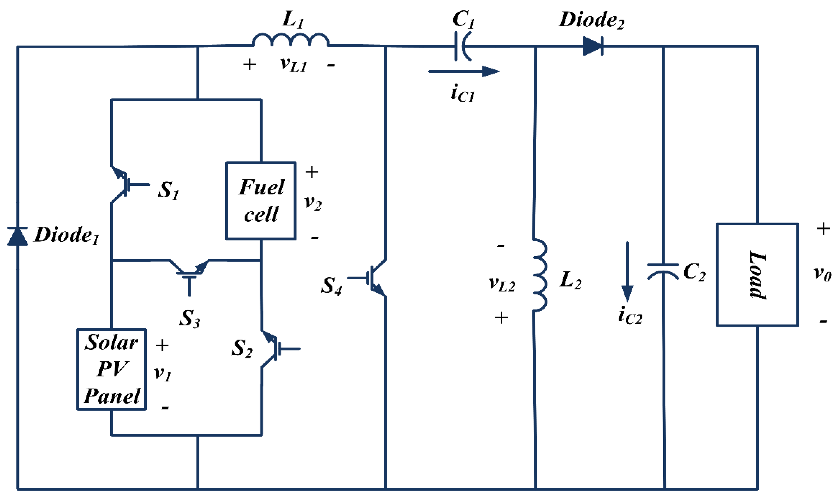
The working principles of the MIC and traditional single input DC-DC converters are nearly identical. In all instances, the L and C components of the converter charge for a period of time before transmitting the stored energy to the load. The proposed converter follows the same operational mechanism. Figure 2 depicts the newly built multi-input DC-DC power electronic converter for GIHEV applications.
We adopted a scientifically approved design approach to develop this converter, as illustrated in Figure 3 [60]. The steps of this design approach are discussing multiple modes of operation, formulating dynamic equations for each mode, constructing a state-space model for each mode, average large-signal modeling, small-signal modeling, and steady-state modeling. Finally, inductor and capacitor values are calculated based on the power level and application. In this converter, the sources can transfer power to the load either collectively or independently using the exemplary action of the power switches. The duty cycles of the power switches S 1 , S 2 , S 3 , and S 4 are regulated to control the flow of power from both inputs to output, as well as to regulate output voltage over a large range.

2.1. Modes of Operation, Dynamic Equations, and State-Space Model

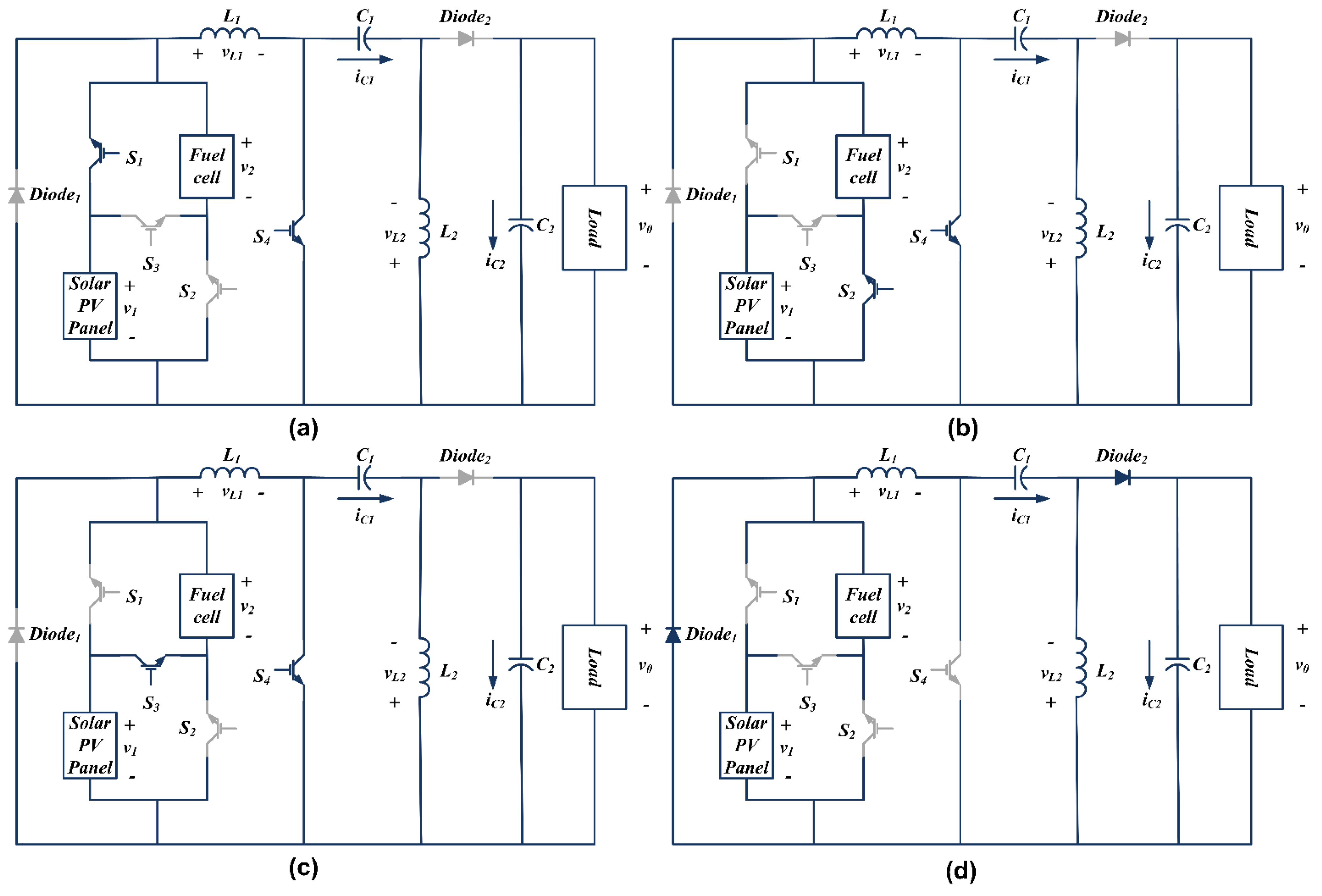
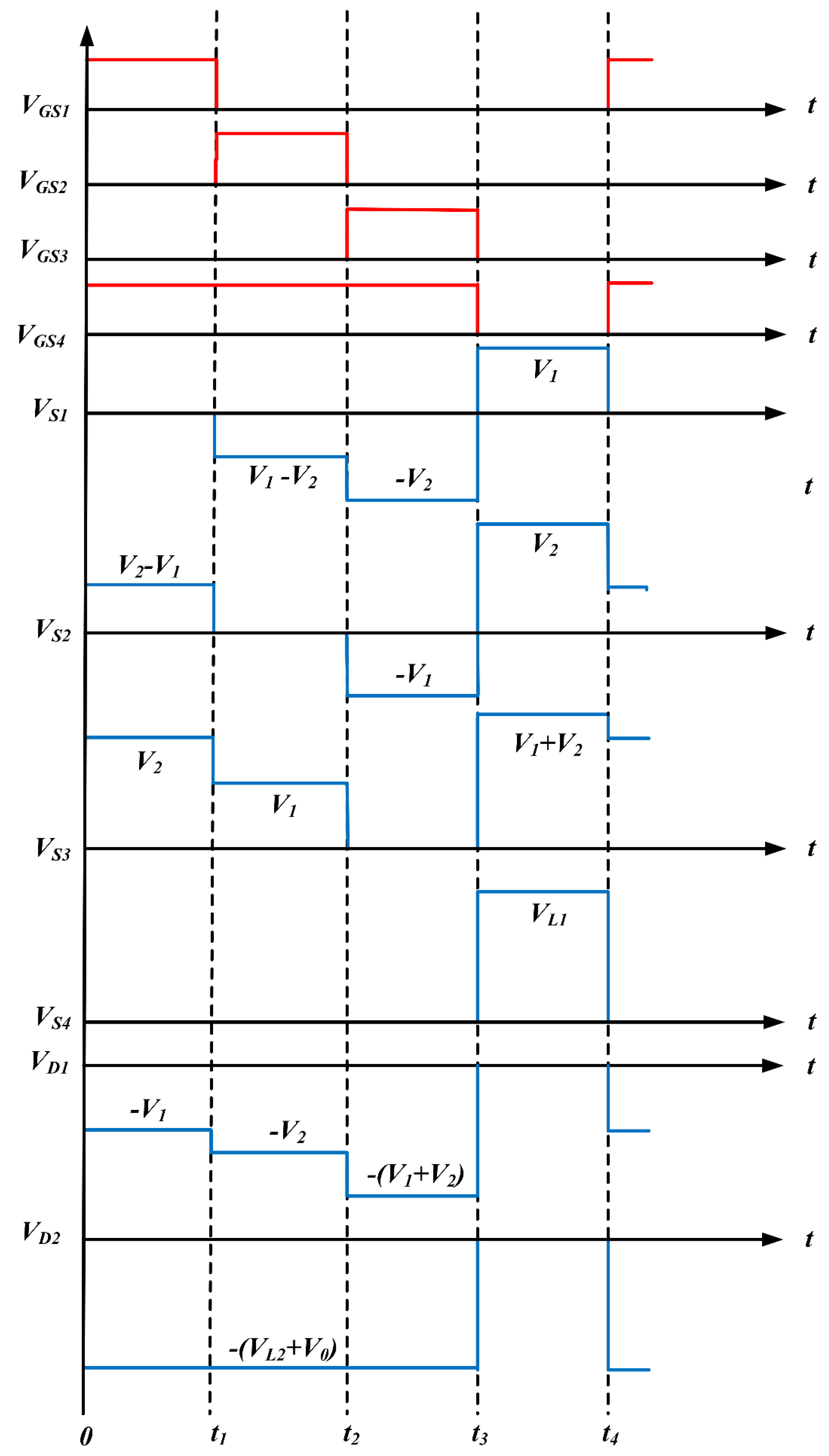
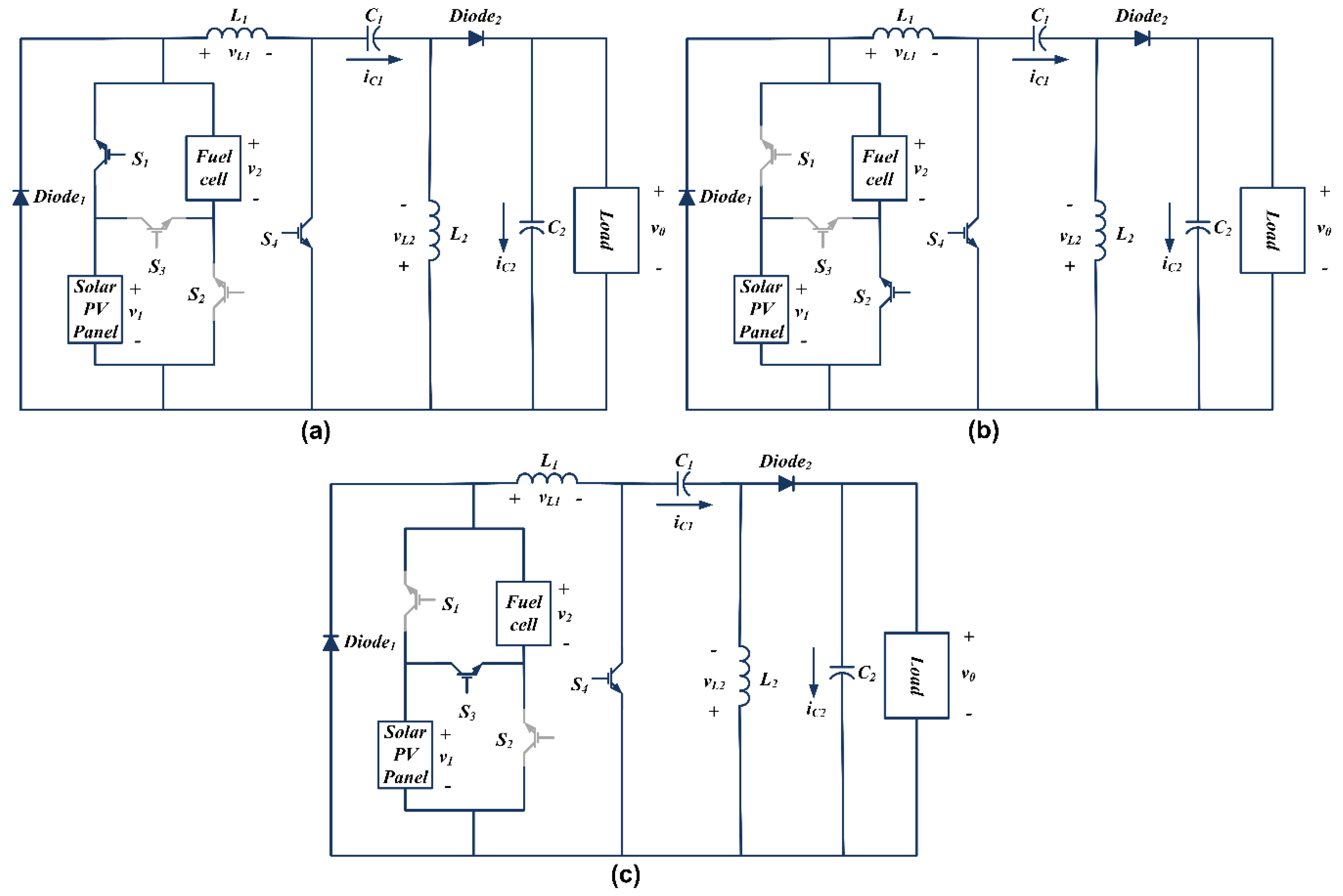
The proposed converter has four modes of operation and the respective equivalent circuits are shown in Figure 4. The ideal waveforms of the proposed fuel cell and solar photovoltaic panel-powered SEPIC-based novel multi-input DC-DC converter for GIHEVs under CCM are shown in Figure 5. In Figure 2, v 1 and v 2 are the large-signal terminal voltages of solar panel and fuel cell, respectively, S 1 to S 4 are the four IGBT switches, D i o d e 1 and D i o d e 2 are two diodes, L 1 and L 2 are the two inductors, C 1 and C 2 are the two capacitors, and R is the load resistance. v L 1 and v L 2 are the large-signal voltages across L 1 and L 2 , respectively, and i L 1 and i L 2 are the large-signal currents flowing through L 1 and L 2 , respectively. i C 1 and i C 2 are the large-signal currents flowing through C 1 and C 2 , respectively, and v 0 is the large-signal voltage across R . In Figure 5, V G S 1 to V G S 4 are the gating pulses of the switches S 1 to S 4 , respectively. v C 1 and v C 2 are the large-signal voltages across C 1 and C 2 , respectively, and i 0 is the large-signal current flowing through R . V 0 is the steady-state voltage across R and I 0 = V 0 / R is the steady-state current flowing through R .
The designed converter is capable of operating at any combination of inputs. To analyze the designed converter’s operation, assume v 2 is greater than v 1 . Consider δ 1 to δ 3 to be the large-signal duty cycles of Mode–1 to Mode–3, respectively, and T to be the time period of the switching pulse. The switching frequency of switches S 1 to S 4 is f s = 1 / T . The intermittent nature of solar energy and the fuel cell system dynamics are not considered in the design process and analysis of the proposed converter. The detailed operation of the proposed converter along with respective dynamic equations and state-space model in each operating mode is discussed from Section 2.1.1, Section 2.1.2, Section 2.1.3 and Section 2.1.4.

2.1.1. Mode–1

In Mode–1, the switches S 1 and S 4 are in the ON condition and S 2 , S 3 , D i o d e 1 , and D i o d e 2 are in the OFF condition. The time period of this mode of operation is from 0 to S 3 , which is equivalent to δ 1 T , as shown in Figure 5. The equivalent circuit of the converter under this mode of operation is shown in Figure 4a. The inductors L 1 and L 2 start charging, the slopes of the inductor currents i L 1 and i L 2 are v 1 / L 1 and v C 1 / L 2 , respectively. The capacitor C 2 starts discharging through the load resistance R , the slope of the capacitor voltage v C 2 is v 0 / R C 2 . The capacitor C 1 starts discharging and helps L 2 to charge, the slope of the capacitor voltage v C 1 is i L 2 / C 1 .
By performing KVL and KCL on Figure 4a, the following equations from (1) to (5) can be derived.
v L 1 = v 1
v L 2 = v C 1
i C 1 = i L 2
i C 2 = i 0
v 0 = v C 2 = i 0 R = i C 2 R
The dynamic equations of Mode–1 are given below.
d i L 1 d t = v 1 L 1
d i L 2 d t = v C 1 L 2
d v C 1 d t = i L 2 C 1
d v C 2 d t = v 0 R C 2
v 0 = v C 2
The order of the proposed system is four, the inductor currents i L 1 and i L 2 and capacitor voltages v C 1 and v C 2 are selected as state variables. By utilizing dynamic equations of Mode–1, the state-space model can be derived as shown in Equations (6) and (7).
[ d i L 1 d t d i L 2 d t d v C 1 d t d v C 1 d t ] = [ 0 0 0 0 0 0 1 L 2 0 0 1 C 1 0 0 0 0 0 1 R C 2 ] [ i L 1 i L 2 v C 1 v C 2 ] + [ 1 L 1 0 0 0 0 0 0 0 ] [ v 1 v 2 ]
v 0 = [ 0 0 0 1 ] [ i L 1 i L 2 v C 1 v C 2 ] + 0

2.1.2. Mode–2

In Mode–2, the switches S 2 and S 4 are in the ON condition and S 1 , S 3 , D i o d e 1 , and D i o d e 2 are in the OFF condition. The time period of this mode of operation is from t 1 to t 2 , which is equivalent to δ 2 T , as shown in Figure 5. The equivalent circuit of the converter under this mode of operation is shown in Figure 4b. The inductors L 1 and L 2 start charging, the slopes of the inductor currents i L 1 and i L 2 are v 2 / L 1 and v C 1 / L 2 , respectively. The capacitor C 2 starts discharging through the load resistance R , the slope of the capacitor voltage v C 2 is v 0 / R C 2 . The capacitor C 1 starts discharging and helps L 2 to charge, the slope of the capacitor voltage v C 1 is i L 2 / C 1 .
By performing KVL and KCL on Figure 4b, the following equations from (8) to (12) can be derived.
v L 1 = v 2
v L 2 = v C 1
i C 1 = i L 2
i C 2 = i 0
v 0 = v C 2 = i 0 R = i C 2 R
The dynamic equations of Mode–2 are given below.
d i L 1 d t = v 2 L 1
d i L 2 d t = v C 1 L 2
d v C 1 d t = i L 2 C 1
d v C 2 d t = v 0 R C 2
v 0 = v C 2
By utilizing dynamic equations of Mode–2, the state-space model can be derived as shown in Equations (13) and (14).
[ d i L 1 d t d i L 2 d t d v C 1 d t d v C 1 d t ] = [ 0 0 0 0 0 0 1 L 2 0 0 1 C 1 0 0 0 0 0 1 R C 2 ] [ i L 1 i L 2 v C 1 v C 2 ] + [ 0 1 L 1 0 0 0 0 0 0 ] [ v 1 v 2 ]
v 0 = [ 0 0 0 1 ] [ i L 1 i L 2 v C 1 v C 2 ] + 0

2.1.3. Mode–3

In Mode–3, the switches S 3 and S 4 are in the ON condition and S 1 , S 2 , D i o d e 1 , and D i o d e 2 are in the OFF condition. The time period of this mode of operation is from t 2 to t 3 , which is equivalent to δ 3 T , as shown in Figure 5. The equivalent circuit of the converter under this mode of operation is shown in Figure 4c. The inductors L 1 and L 2 start charging, the slopes of the inductors currents i L 1 and i L 2 are ( v 1 + v 2 ) / L 1 and v C 1 / L 2 , respectively. The inductor currents i L 1 and i L 2 reach their maximum values i L 1 max and i L 2 max , respectively. The capacitor C 2 starts discharging through the load resistance R , the slope of the capacitor voltage v C 2 is v 0 / R C 2 . The capacitor C 1 starts discharging and helps L 2 to charge, the slope of the capacitor voltage v C 1 is i L 2 / C 1 .
By performing KVL and KCL on Figure 4c, the following equations from (15) to (19) can be derived.
v L 1 = v 1 + v 2
v L 2 = v C 1
i C 1 = i L 2
i C 2 = i 0
v 0 = v C 2 = i 0 R = i C 2 R
The dynamic equations of Mode–3 are given below.
d i L 1 d t = v 1 + v 2 L 1
d i L 2 d t = v C 1 L 2
d v C 1 d t = i L 2 C 1
d v C 2 d t = v 0 R C 2
v 0 = v C 2
By utilizing dynamic equations of Mode–3, the state-space model can be derived as shown in Equations (20) and (21).
[ d i L 1 d t d i L 2 d t d v C 1 d t d v C 1 d t ] = [ 0 0 0 0 0 0 1 L 2 0 0 1 C 1 0 0 0 0 0 1 R C 2 ] [ i L 1 i L 2 v C 1 v C 2 ] + [ 1 L 1 1 L 1 0 0 0 0 0 0 ] [ v 1 v 2 ]
v 0 = [ 0 0 0 1 ] [ i L 1 i L 2 v C 1 v C 2 ] + 0

2.1.4. Mode–4

In Mode–4, the diodes D i o d e 1 and D i o d e 2 are in the ON condition and S 1 , S 2 , S 3 , and S 4 are in the OFF condition. The time period of this mode of operation is from t 3 to t 4 , which is equivalent to ( 1 δ 1 δ 2 δ 3 ) T , as shown in Figure 5. The equivalent circuit of the converter under this mode of operation is shown in Figure 4d. The inductors L 1 and L 2 start discharging, the slopes of the inductor currents i L 1 and i L 2 are ( v C 1 v C 2 ) / L 1 and v C 2 / L 2 , respectively. The inductor current i L 1 reaches its minimum value i L 1 min from its maximum value i L 1 max . The inductor current i L 2 reaches its minimum value i L 2 min from its maximum value i L 2 max . The capacitors C 1 and C 2 starts charging with the help of L 1 and L 2 , the slopes of the capacitor voltages v C 1 and v C 2 are i L 1 / C 1 and ( ( i L 1 / C 2 ) + ( i L 2 / C 2 ) ( v C 2 / R C 2 ) ) , respectively.
By performing KVL and KCL on Figure 4d, the following equations from (22) to (25) can be derived.
v L 1 = v C 1 v C 2
v L 2 = v 0
i L 1 = i C 1
i L 2 = i 0 + i C 2 i L 1
The dynamic equations of Mode–4 are given below.
d i L 1 d t = v C 1 v C 2 L 1
d i L 2 d t = v C 2 L 2
d v C 1 d t = i L 1 C 1
d v C 2 d t = i L 1 C 2 + i L 2 C 2 v C 2 R C 2
v 0 = v C 2
By utilizing dynamic equations of Mode–4, the state-space model can be derived as shown in Equations (26) and (27).
[ d i L 1 d t d i L 2 d t d v C 1 d t d v C 1 d t ] = [ 0 0 1 L 1 1 L 1 0 0 0 1 L 2 1 C 1 0 0 0 1 C 2 1 C 2 0 1 R C 2 ] [ i L 1 i L 2 v C 1 v C 2 ] + [ 0 0 0 0 0 0 0 0 ] [ v 1 v 2 ]
v 0 = [ 0 0 0 1 ] [ i L 1 i L 2 v C 1 v C 2 ] + 0

2.2. Average Large-Signal Modeling

The proposed converter is a non-linear circuit. The average large-signal modeling approach takes non-linearity and the effects of the circuit’s real voltages into account, so the obtained results are very near to those of the real circuit.
The state-space representation of average large-signal model is as follows.
x ˙ = A x + B u
y = C x + D u
where A is an average large-signal model system matrix, B is an average large-signal model input matrix, C is an average large-signal model output matrix, and D is an average large-signal model feed forward matrix.
From Equations (6), (7), (13), (14), (20), (21), (26) and (27), the matrices A , B , and C are calculated as shown in Equations (28) to (30) and the matrix D is a null matrix.
A = [ 0 0 0 0 0 0 1 L 2 0 0 1 C 1 0 0 0 0 0 1 R C 2 ] ( δ 1 + δ 2 + δ 3 ) + [ 0 0 1 L 1 1 L 1 0 0 0 1 L 2 1 C 1 0 0 0 1 C 2 1 C 2 0 1 R C 2 ] ( 1 δ 1 δ 2 δ 3 )
B = [ 1 L 1 ( δ 1 + δ 3 ) 1 L 1 ( δ 2 + δ 3 ) 0 0 0 0 0 0 ]
C = [ 0 0 0 1 ]

2.3. Small-Signal Modeling

The small-signal modeling linearizes the entire system’s components. In order to develop the small-signal model of the proposed converter, we introduce perturbations in state variables, input variables, and control variables. The state variables, input variables, and control variables consist of two components, a DC component and perturbation component.
v 1 = V 1 + v ^ 1
v 2 = V 2 + v ^ 2
i L 1 = I L 1 + i ^ L 1
i L 2 = I L 2 + i ^ L 2
v C 1 = V C 1 + v ^ C 1
v C 2 = V C 2 + v ^ C 2
δ 1 = d 1 + δ ^ 1
δ 2 = d 2 + δ ^ 2
δ 3 = d 3 + δ ^ 3
where V 1 and V 2 are the steady-state (DC component) voltages of the solar panel and fuel cell, respectively. I L 1 and I L 2 are the steady-state current flowing through L 1 and L 2 , respectively. V C 1 and V C 2 are the steady-state voltages across C 1 and C 2 , respectively. d 1 to d 3 are the steady-state duty cycle of Mode–1 to Mode–3, respectively. v ^ 1 and v ^ 2 are the small-signal (perturbation component) voltages of the solar panel and fuel cell, respectively. i ^ L 1 and i ^ L 2 are the small-signal current flowing through L 1 and L 2 , respectively. v ^ C 1 and v ^ C 2 are the small-signal voltages across C 1 and C 2 , respectively. δ ^ 1 to δ ^ 3 are the small-signal duty cycle of Mode–1 to Mode–3, respectively.
Including perturbations in Equations (28)–(30), the resultant state-space representation is given by Equations (31) and (32).
[ d i ^ L 1 d t d i ^ L 2 d t d v ^ C 1 d t d v ^ C 2 d t ] = [ 0 0 1 L 1 ( 1 d 1 d 2 d 3 ) 1 L 1 ( 1 d 1 d 2 d 3 ) 0 0 1 L 2 ( d 1 + d 2 + d 3 ) 1 L 2 ( 1 d 1 d 2 d 3 ) 1 C 1 ( 1 d 1 d 2 d 3 ) 1 C 1 ( d 1 + d 2 + d 3 ) 0 0 1 C 2 ( 1 d 1 d 2 d 3 ) 1 C 2 ( 1 d 1 d 2 d 3 ) 0 1 R C 2 ] [ i ^ L 1 i ^ L 2 v ^ C 1 v ^ C 2 ] + [ 1 L 1 ( V C 1 + V C 2 + V 1 ) 1 L 1 ( V C 1 + V C 2 + V 2 ) 1 L 1 ( V C 1 + V C 2 + V 1 + V 2 ) 1 L 1 ( d 1 + d 3 ) 1 L 1 ( d 2 + d 3 ) 1 L 2 ( V C 1 + V C 2 ) 1 L 2 ( V C 1 + V C 2 ) 1 L 2 ( V C 1 + V C 2 ) 0 0 1 C 1 ( I L 1 + I L 2 ) 1 C 1 ( I L 1 + I L 2 ) 1 C 1 ( I L 1 + I L 2 ) 0 0 1 C 2 ( I L 1 + I L 2 ) 1 C 2 ( I L 1 + I L 2 ) 1 C 2 ( I L 1 + I L 2 ) 0 0 [ δ ^ 1 δ ^ 2 δ ^ 3 v ^ 1 v ^ 2 ]
v ^ 0 = [ 0 0 0 1 ] [ i ^ L 1 i ^ L 2 v ^ C 1 v ^ C 2 ]
By comparing Equations (31) and (32) above with general state-space representation as shown in Equation (33) below, the matrix A ^ is identified.
x ^ ˙ = A ^ x ^ + B ^ u ^ y ^ = C ^ x ^ + D ^ u ^ }
where A ^ is a small-signal model system matrix, B ^ is a small-signal model input matrix, C ^ is a small-signal model output matrix, and D ^ is a small-signal model feed forward matrix. x ^ is a small-signal model state vector matrix, x ^ ˙ is a first derivative of the small-signal model state vector matrix, u ^ is a small-signal model input vector matrix, and y ^ is a small-signal model output vector matrix.
The characteristic equation is
| A ^ S I | = 0
where S is the Laplace transform variable and I is the identity matrix of order 4 × 4.
S 4 + S 3 1 R C 2 + S 2 ( ( d 1 + d 2 + d 3 ) 2 C 1 L 2 + ( 1 d 1 d 2 d 3 ) 2 C 2 L 2 + ( 1 d 1 d 2 d 2 ) 2 C 1 L 1 + ( 1 d 1 d 2 d 3 ) 2 C 2 L 1 ) + S ( ( d 1 + d 2 + d 3 ) 2 R C 1 C 2 L 2 + ( 1 d 1 d 2 d 3 ) 2 R C 1 C 2 L 1 ) + 1 C 1 C 2 L 1 L 2 ( ( 1 d 1 d 2 d 3 ) 4 + 2 ( 1 d 1 d 2 d 3 ) 3 ( d 1 + d 2 + d 3 ) + ( 1 d 1 d 2 d 3 ) 2 ( d 1 + d 2 + d 3 ) 2 ) = 0
Compare Equation (34) with the equation below:
S 4 + S 3 a + S 2 b + S c + d = 0 .
As the order of the system is four, instead of using a pole-zero plot, the RHSC technique is employed to find the stability of the proposed converter to avoid the difficulty of finding poles and zeros of higher order systems. The R-H stability criterion table is shown below.
S 4 S 3 S 2 S 1 S 0 | 1 b d a c 0 a b c a d 0 a b c c 2 a 2 d a b c 0 0 d 0 0
From the R-H stability criterion table, all the coefficients of Equation (34) are positive, real, and non-zero. Furthermore, all the elements of the first column of the R-H stability criterion table are positive. Therefore, the system is stable under any duty cycle value, which is less than the maximum allowable value.

2.4. Steady-State Modeling

The steady-state modeling helps to find output voltage and current expressions in terms of duty cycle and also helps to design the system parameters. We replace variables with steady-state variables in all average large-signal equations. Consider that V 1 and V 2 are the steady-state solar panel and fuel cell voltages, respectively. V L 1 and V L 2 are the steady-state voltage across L 1 and L 2 , respectively, and I L 1 and I L 2 are the steady-state current flowing through L 1 and L 2 , respectively. V C 1 and V C 2 are the steady-state voltages across C 1 and C 2 , respectively, and I C 1 and I C 2 are the steady-state current flowing through C 1 and C 2 , respectively. I D 1 and I D 2 are the steady-state currents flowing through diodes D i o d e 1 and D i o d e 2 . I 1 and I 2 are the steady-state current flowing from the source solar panel and fuel cell, respectively.
From Equations (1)–(5), (8)–(12), (15)–(19) and (22)–(25),
Volt-Sec balance equation at L 1 ,
V 1 d 1 T + V 2 d 2 T + ( V 1 + V 2 ) d 3 T + ( V C 1 V 0 ) ( 1 d 1 d 2 d 3 ) T = 0 .
By simplifying the above equation,
V 1 ( d 1 + d 3 ) + V 2 ( d 2 + d 3 ) V C 1 ( 1 d 1 d 2 d 3 ) V 0 ( 1 d 1 d 2 d 3 ) = 0 .
Volt-Sec balance equation at L 2 ,
V C 1 d 1 T + V C 1 d 2 T + V C 1 d 3 T V 0 ( 1 d 1 d 2 d 3 ) T = 0 .
By simplifying the above equation,
V C 1 = V 0 ( 1 d 1 d 2 d 3 d 1 + d 2 + d 3 ) .
Substitute Equation (35) in (36) to find the expression for output voltage as shown in Equation (37).
V 0 = d 1 + d 2 + d 3 1 d 1 d 2 d 3 ( V 1 ( d 1 + d 3 ) + V 2 ( d 2 + d 3 ) )
Amp-Sec balance equation at C 1 ,
I L 2 d 1 T I L 2 d 2 T I L 2 d 3 T + I L 1 ( 1 d 1 d 2 d 3 ) T = 0 .
By simplifying the above equation,
I L 2 ( d 1 + d 2 + d 3 ) + I L 1 ( 1 d 1 d 2 d 3 ) = 0 .
Amp-Sec balance equation at C 2 ,
I 0 d 1 T I 0 d 2 T I 0 d 3 T + ( I L 1 + I L 2 I 0 ) ( 1 d 1 d 2 d 3 ) T = 0 .
By simplifying the above equation,
I L 2 ( 1 d 1 d 2 d 3 ) + I L 1 ( 1 d 1 d 2 d 3 ) = I 0 .
By solving Equations (38) and (39),
I L 2 = I 0 = V 0 R
I L 1 = V 0 R d 1 + d 2 + d 3 1 d 1 d 2 d 3 .

2.4.1. Effect of Parasitic Elements

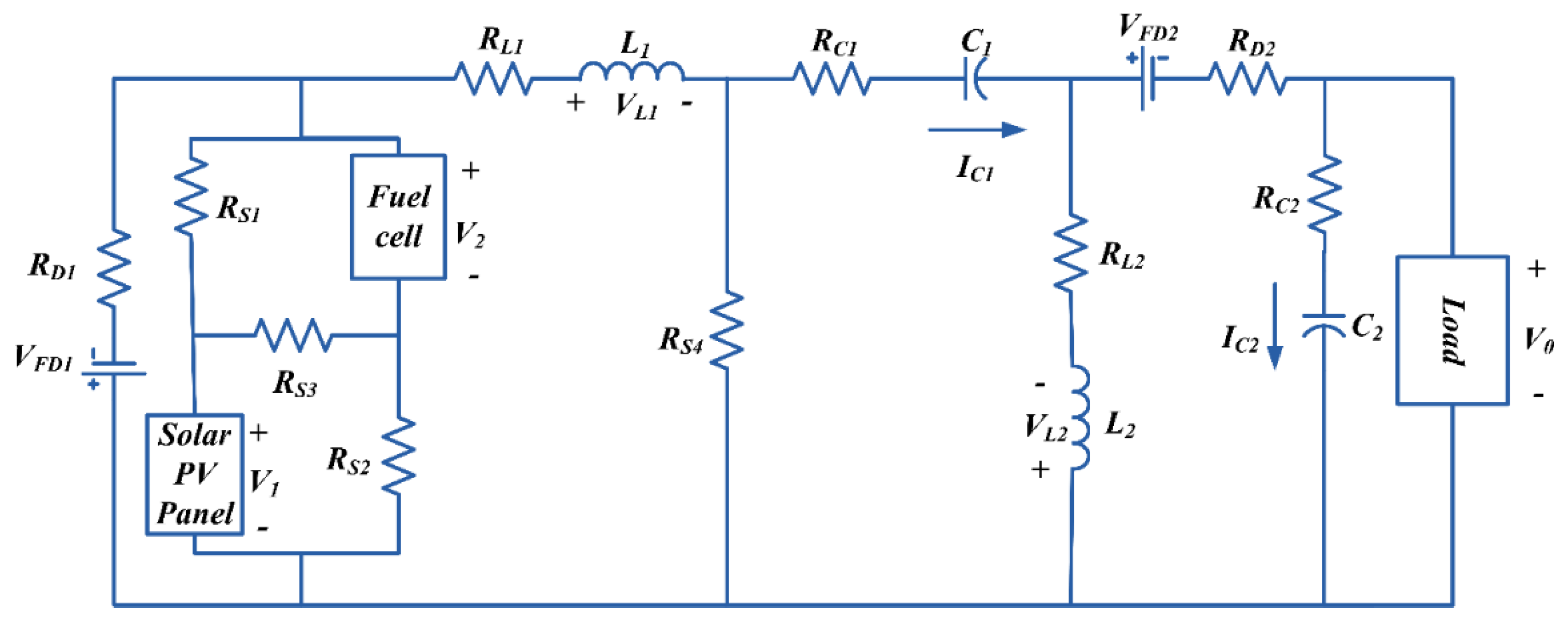
Figure 6 shows the proposed converter with parasitic elements, where R L 1 , R L 2 , R C 1 , and R C 2 are the internal resistance of L 1 , L 2 , C 1 , and C 2 , respectively, and R S 1 , R S 2 , R S 3 , R S 4 , R D 1 , and R D 2 are the on-state resistance of S 1 , S 2 , S 3 , S 4 , D i o d e 1 , and D i o d e 2 . V F D 1 and V F D 2 are the forward bias voltages of diodes D i o d e 1 and D i o d e 2 .
The output voltage expression by considering parasitic elements is given in Equation (42).
V 0 = d 1 + d 2 + d 3 1 d 1 d 2 d 3 ( V 1 ( d 1 + d 3 ) + V 2 ( d 2 + d 3 ) V F D 1 ( 1 d 1 d 2 d 3 d 1 + d 2 + d 3 ) V F D 2 ( 1 d 1 d 2 d 3 ) )   1 + A 10 + A 11 + A 12 + A 13 + A 14 + A 15 + A 16
where
A 10 = R L 2 R
A 11 = R D 2 R 1 1 d 1 d 2 d 3
A 12 = R D 1 R ( ( d 1 + d 2 + d 3 ) 2 1 d 1 d 2 d 3 )
A 13 = ( d 1 + d 2 + d 3 ) 2 ( 1 d 1 d 2 d 3 ) 2 ( R S 1 R d 1 + R S 2 R d 2 + R S 3 R d 3 )
A 14 = R S 4 R ( d 1 + d 2 + d 3 ) ( 1 + 2 ( d 1 + d 2 + d 3 ) ( 1 d 1 d 2 d 3 ) + ( d 1 + d 2 + d 3 ) 2 ( 1 d 1 d 2 d 3 ) 2 )
A 15 = R L 1 R ( ( d 1 + d 2 + d 3 ) 2 ( 1 d 1 d 2 d 3 ) 2 )
A 16 = R C 1 R ( ( 2 ( d 1 + d 2 + d 3 ) 1 ) ( d 1 + d 2 + d 3 ) ( 1 d 1 d 2 d 3 ) ) .
The parasitic elements have a big influence on the converter’s gain and efficiency. Equation (42) can be used to compute the gain, and Section 3 discusses power losses and efficiency calculations.

2.4.2. Inductor and Capacitor Selection

The proper selection of inductors and capacitors impacts the system performance by allowing the converter to function in the desired conduction mode.
The value of L 1 is given by Equation (43).
L 1 = ( V 1 ( d 1 + d 3 ) + V 2 ( d 2 + d 3 ) ) T Δ I L 1
where Δ I L 1 is the change in I L 1 . The expression of Δ I L 1 is shown in Equation (44).
Δ I L 1 = I L 1 m a x I L 1 m i n
The value of L 2 is given by Equation (45).
L 2 = V 0 ( 1 d 1 d 2 d 3 ) T Δ I L 2
where Δ I L 2 is the change in I L 2 . The expression of Δ I L 2 is shown in Equation (46).
Δ I L 2 = I L 2 m a x I L 2 m i n
The value of C 1 is given by Equation (47).
C 1 = V 0 ( d 1 + d 2 + d 3 ) T R Δ V C 1
where Δ V C 1 is the change in V C 2 . The expression of Δ V C 1 is shown in Equation (48).
Δ V C 1 = V C 1 m a x V C 1 m i n
The value of C 2 is given by Equation (49).
C 2 = V 0 ( d 1 + d 2 + d 3 ) T R Δ V C 2
where Δ V C 2 is the change in V C 2 . The expression of Δ V C 2 is shown in Equation (50).
Δ V C 2 = V C 2 m a x V C 2 m i n

2.4.3. Condition for DCM

The proposed converter’s CCM operation in discussed in this paper. The condition to maintain its operation in CCM is given below and also shown in Figure 7.
The design and selection of inductor L 1 and L 2 should follow Equations (51) and (52), respectively, to maintain the system operation in CCM.
2 L 1 R T > V 1 ( d 1 + d 3 ) + V 2 ( d 2 + d 3 ) V 0 ( 1 d 1 d 2 d 3 ) ( d 1 + d 2 + d 3 )
2 L 2 R T > ( 1 d 1 d 2 d 3 ) 1
where 2 L 1 / R T and 2 L 2 / R T are the time constants of L 1 and L 2 , respectively.
If the design fails to follow the conditions shown in the above two Equations ((51) and (52)), the system will start operating in DCM.

3. Voltage Stress and Efficiency Calculations

3.1. Voltage Stress Calculations

When choosing the best power switches and diodes, voltage stress is a crucial factor to consider. As a result, it is necessary to determine the voltage stresses. When a power electronic switch is turned off, the voltage stress is equal to the maximum voltage magnitude across the switch. Figure 8 shows the voltage waveforms of power switches and diodes, as well as the gating pulses of the proposed converter.
The voltage stress of S 1 ( V V S 1 ) is given below.
V V S 1 = max ( 0 ,   V 1 V 2 , V 2 ,   V 1 ) = V 2
The voltage stress of S 2 ( V V S 2 ) is given below.
V V S 2 = max ( V 2 V 1 ,   0 , V 1 ,   V 2 ) = V 2
The voltage stress of S 3 ( V V S 3 ) is given below.
V V S 3 = max ( V 2 ,   V 1 ,   0 , V 1 + V 2 ) = V 1 + V 2
The voltage stress of S 4 ( V V S 4 ) is given below.
V V S 4 = max ( 0 ,   0 ,   0 , V L 1 ) = V L 1 = V C 1 + V 0 = 1 1 d 1 d 2 d 3 ( V 1 ( d 1 + d 3 ) + V 2 ( d 2 + d 3 ) )
The voltage stress of D i o d e 1 ( V V S D 1 ) is given below.
V V S D 1 = max ( V 1 , V 2 , ( V 1 + V 2 ) ,   0 ) = V 1 + V 2
The voltage stress of D i o d e 2 ( V V S D 2 ) is given below.
V V S D 2 = max ( V L 2 V 0 , V L 2 V 0 , V L 2 V 0 ,   0 ) = V L 2 + V 0 = V C 1 + V 0 = 1 1 d 1 d 2 d 3 ( V 1 ( d 1 + d 3 ) + V 2 ( d 2 + d 3 ) )

3.2. Efficiency Calculations

Power loss calculation due to the parasitic elements is given below
Power   loss   due   to   the   parasitic   elements = j = 1 4 P S j + j = 1 2 P R L j + j = 1 2 P R C j + j = 1 2 P R D j + j = 1 2 P V F D j = I S 1 R 2 R S 1 + I S 2 R 2 R S 2 + I S 3 R 2 R S 3 + I S 4 R 2 R S 4 + I L 1 R 2 R L 1 + I L 2 R 2 R L 2 + I C 1 R 2 R C 1 + I C 2 R 2 R C 2 + I D R 1 2 R D 1 + I D R 2 2 R D 2 + I D a v g 1 V F D 1 + I D a v g 2 V F D 2
where P S 1 , P S 2 , P S 3 , P S 4 , P R L 1 , P R L 2 , P R C 1 , P R C 2 , P R D 1 , and P R D 2 are the ohmic losses of S 1 , S 2 , S 3 , S 4 , L 1 , L 2 , C 1 , C 2 , D i o d e 1 , and D i o d e 2 , respectively. P V F D 1 and P V F D 1 are the power loss due to V F D 1 and V F D 1 . I S 1 R , I S 2 R , I S 3 R , I S 4 R , I L 1 R , I L 2 R , I C 1 R , I C 2 R , I D R 1 , and I D R 2 are the RMS value of currents flowing through S 1 , S 2 , S 3 , S 4 , L 1 , L 2 , C 1 , C 2 , D i o d e 1 , and D i o d e 2 , respectively. I D a v g 1 and I D a v g 2 are the average value of current flowing through D i o d e 1 and D i o d e 2 , respectively.
Switching losses of the switches are given below.
Switching   losses   of   the   switches = j = 1 4 P S j S W = 1 2 j = 1 4 V S j I S j P ( t o n S j + t o f f S j ) f s + 1 2 j = 1 4 V S j 2 C O S S f s
Here, P S 1 S W , P S 2 S W , P S 3 S W , and P S 4 S W are the switching losses of S 1 , S 2 , S 3 , and S 4 , respectively. V S 1 , V S 2 , V S 3 , and V S 4 are voltage across the switches S 1 , S 2 , S 3 , and S 4 , respectively. I S 1 P , I S 2 P , I S 3 P , and I S 4 P are the peak value of currents flowing through switches S 1 , S 2 , S 3 , and S 4 , respectively. t o n S 1 , t o n S 2 , t o n S 3 , and t o n S 4 are the on-state time period of switches S 1 , S 2 , S 3 , and S 4 , respectively. t o f f S 1 , t o f f S 2 , t o f f S 3 , and t o f f S 4 are the off-state time period of switches S 1 , S 2 , S 3 , and S 4 , respectively. The C O S S is the output capacitance of the switches.
The total power loss of the converter is
P L o s s = Power   loss   due   to   the   parasitic   elements + Switching   losses .
Therefore, the efficiency of the converter is
% E f f i c i e n c y = P o u t P o u t + P L o s s × 100 ,
where P o u t is the output power of the proposed converter. At specified inputs and duty cycles, the proposed converter provides the required power to the load at the rated output voltage with great efficiency and accuracy.

4. Possible Operating Scenarios

In addition to the six modes of operation, the proposed converter can also be operated in three other ways, each with its own output voltage expressions, as shown in Table 1, where D 4 is the duty ratio of switch S 4 and, similarly, D 1 , D 2 , and D 3 are the duty ratios of switches S 1 , S 2 , and S 3 , respectively. The equivalent circuits of possible operating scenarios of the proposed converter are shown in Figure 9.

4.1. Solar PV Panel Alone Supplying the Load

In Scenario–2, the suggested converter can provide all of the required power to the load using only a solar PV panel. Figure 9a depicts the power circuit for this operation. As shown in Figure 4, this power circuit has two modes of operation: Mode–1 and Mode–4 of the original circuit. This potential operating situation would allow the vehicle to run solely on solar energy. This process will assist the vehicle in avoiding the use of hydrogen, lowering the vehicle’s operating costs to nearly nothing. The voltage at the output terminals in this scenario is
V 0 = V 1 D 4 1 D 4 ;   D 1 = 1 .

4.2. Fuel Cell Alone Supplying the Load

In Scenario–1, the designed converter can provide all of the required power to the load using only the fuel cell. Figure 9b depicts the power circuit for this operation. As shown in Figure 4, this power circuit has two modes of operation: Mode–2 and Mode–4 of the original circuit. The automobile will be able to operate in the absence of daylight in this scenario. The voltage at the output terminals in this scenario is
V 0 = V 2 D 4 1 D 4 ;   D 2 = 1 .

4.3. Fuel Cell Plus Solar PV Panel Supplying the Load

In Scenario–3, with the help of a fuel cell and a solar PV panel, the designed converter can provide the required power to the load. Figure 9c depicts the power circuit for this procedure. This power circuit operates in two modes: Mode–3 and Mode–4 of the original circuit, as depicted in Figure 4. The vehicle will be able to run on hydrogen and solar light in this conceivable operational condition. The converter will be operated under this condition when the solar PV panel alone is unable to give the required power to the load. This action will assist the vehicle in reducing hydrogen usage, lowering the vehicle’s operating costs. The voltage at the output terminals in this scenario is
V 0 = ( V 1 + V 2 ) D 4 1 D 4 ;   D 3 = 1 .

5. Results Discussion and Analysis

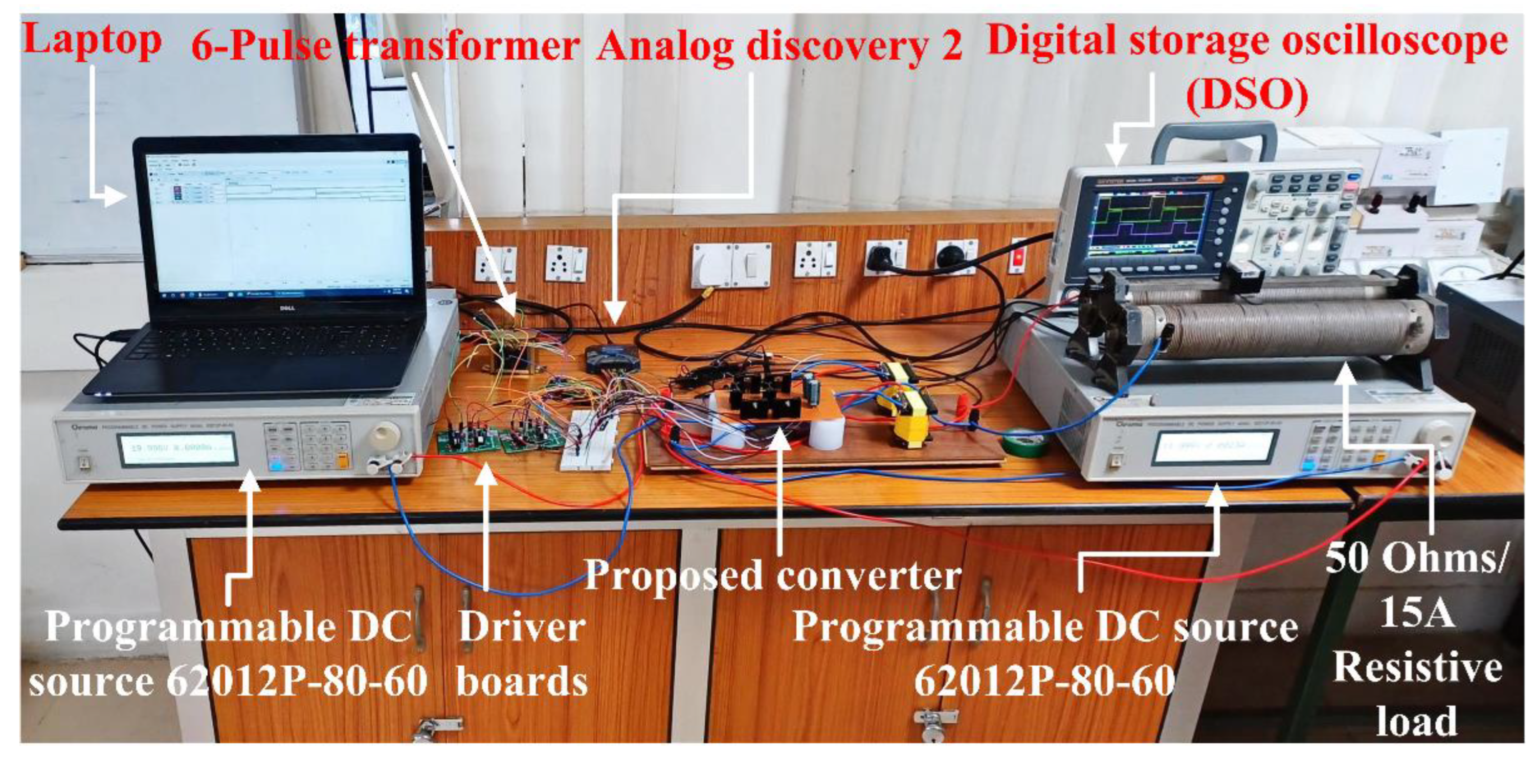
The steady-state behavior of the proposed fuel cell and solar photovoltaic panel powered SEPIC-based novel multi-input DC-DC converter for GIHEVs in CCM is addressed in this research paper. Isolated-gate bipolar transistors (IGBTs) are employed to carry out the switching operation with switching frequency of 10 kHz. A laboratory-based experimental setup is implemented to test the designed converter’s effectiveness. The solar PV panel voltage is V 1 = 12 V and the fuel cell voltage is considered as V 2 = 20 V. By utilizing V 1 and V 2 , the proposed converter is designed to operate at 48 V output voltage and 230 W output power. The experimental setup of the designed converter is shown in Figure 10, and the design parameters are shown in Table 2. Experimentally generated gating pulses of the four IGBT switches V G S 1 , V G S 2 , V G S 3 , and V G S 4 along with the respective pulse amplitude 17 V, switching frequency 10 kHz, and duty cycles are shown in Figure 11a. The duty cycles of S 1 , S 2 , S 3 , and S 4 are 25.071 %, 25.071 %, 25.071 %, and 74.97 %, respectively.
The experimental waveforms of inductor voltages V L 1 and V L 2 and currents I L 1 and I L 2 are shown in Figure 11b. The DC RMS values of V L 1 , V L 2 , I L 1 , and I L 2 are 38.1 V, 27.9 V, 15.3 A, and 5.06 A, respectively. The experimental waveforms of input and output voltages are shown in Figure 11c. The DC RMS values of V 1 , V 2 , and V 0 are 12.3 V, 19.9 V, and 46.9 V, respectively. The experimental waveforms of capacitor voltages V C 1 and V C 2 and currents I C 1 and I C 2 are shown in Figure 11d. The DC RMS values of V C 1 , V C 2 , I C 1 , and I C 2 are 14.4 V, 46.6 V, 9.10 A, and 9.40 A, respectively. The experimental waveforms of switches’ collector to emitter voltages V S 1 , V S 2 , V S 3 , and V S 4 along with respective maximum values are shown in Figure 11e. The voltage stresses of S 1 and S 2 are almost equal to the highest value of input voltage. In the case of S 3 , the voltage stress is equal to the sum of input voltages. The voltage stress of S 4 is 66 V which is less than twice the output voltage. Figure 11f shows the experimental waveforms of the diode’s anode to cathode voltages along with respective maximum values that describe the voltage stress across the diodes. In the case of D i o d e 1 , the voltage stress is equal to the sum of input voltages. The voltage stress of D i o d e 2 is 66 V which is less than twice the output voltage. Figure 12a shows the output voltage variation as a function of duty cycle; the suggested converter can operate at a wide range of voltages with lower duty ratios. The proposed converter enables the sources to supply power to the load either separately or collectively at the rated output voltage with reduced turn-on time of each switch. The suggested converter can also operate in buck mode, as shown in Figure 12a, however, boost operation is validated in this research in order to use the proposed converter in GIHEV applications. Figure 12b shows the efficiency variation with varying load conditions; the suggested converter’s efficiency is 96% at the selected duty cycle and rated load.
The information about losses in the proposed converter is illustrated in Figure 13. As per Figure 13a, among 4% power loss of the proposed converter, 90% losses are conduction losses, and 10% losses are switching losses. Figure 13b describes the loss distribution among power electronic switches in the designed converter. The D i o d e 2 dissipates the maximum share (54%) of the losses and the D i o d e 1 dissipates 39% of the total losses. The switches S 1 , S 2 , S 3 , and S 4 are dissipating 1%, 1%, 1%, and 4% of the losses, respectively.
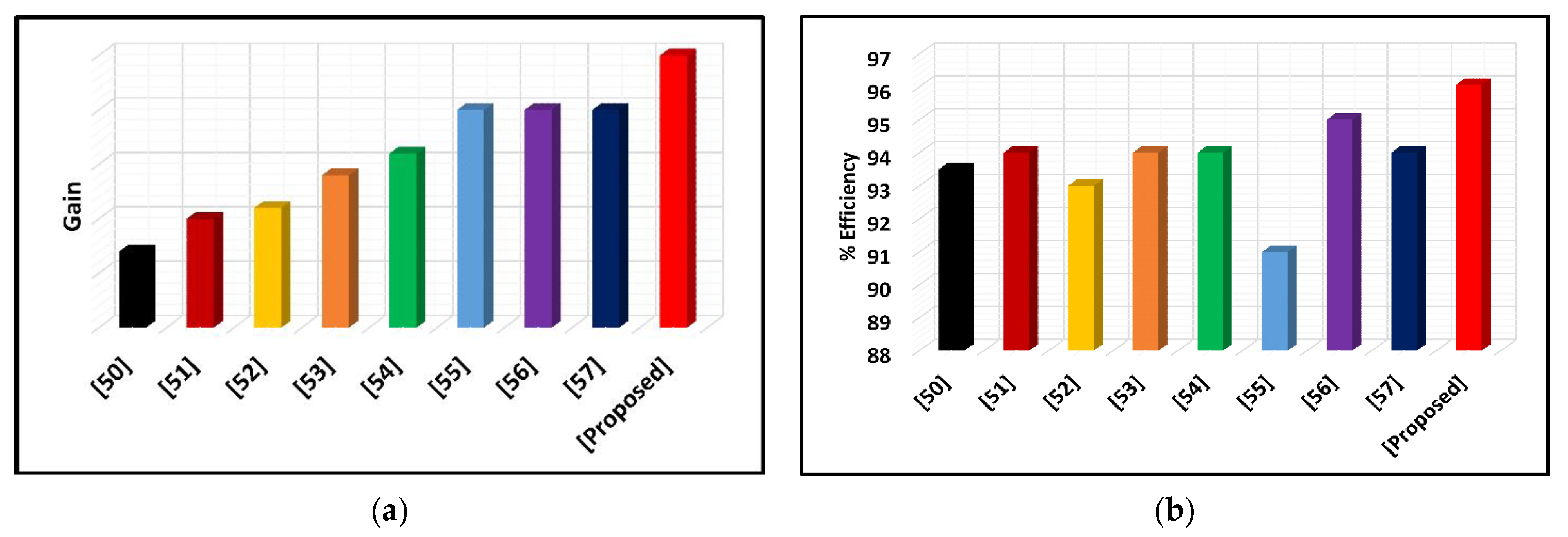
The suggested converter is compared to known topologies in terms of efficiency and gain in Figure 14a,b. Table 3 shows a comparison of the proposed converter with some of the existing converters. When compared to [50], the suggested converter uses fewer total circuit components and has lower voltage stress. The number of total circuit components in the proposed converter is lower, and it delivers a greater gain at a higher efficiency than in [51]. Ref. [52] describes a lower efficiency and a higher number of switching devices than the suggested converter since it uses three relays in addition to the power electronic switches to achieve the necessary operation. In comparison to the converter presented in [53], the proposed converter has higher efficiency, excessive gain with the same output voltage polarity, and lower voltage stress. The proposed converter is good at the number of power electronic switches and efficiency, and it also avoids using the battery as one of the inputs when compared to [54]. The designed converter can provide higher efficiency, higher gain, and lower voltage stress with a smaller number of switches and storage components when compared to [55]. The presented converter in [56] has a higher component count, and a few switches have higher voltage stress than the proposed converter. Moreover, it has eight energy storage elements for the two-input circuit, and it is challenging to analyze the system and design a control logic compared to the proposed converter. The proposed converter has a smaller number of power electronic switches and energy storage elements with lower voltage stress and higher efficiency than [57]. Finally, with positive output voltage across the load, the suggested converter has a high gain, fewer components, lower voltage stress, and improved efficiency.

6. Conclusions

In this work, the design and analysis of the proposed SEPIC-based novel multi-input DC-DC converter with high gain for grid-independent hybrid electric vehicles (GIHEVs) are effectively demonstrated and validated with a hardware prototype. This converter actively adapted both a fuel cell and solar photovoltaic panel to provide the load with continuous power. The proposed optimized topology and design allow the proposed converter to operate at a wide range of output voltages and with power flow regulation at lower duty cycle ratios. To achieve accurate design and improved analysis of the suggested converter, average large-signal modeling, small-signal modeling, and steady-state modeling are established. The proposed converter’s stability is examined using the R-H stability criterion for the first time in this research. The output voltage expression of the converter is obtained from the converter’s steady-state modeling. The proposed converter’s possible operating scenarios with corresponding equivalent circuitry are also discussed, along with the proper operation of the power switches to transmit power to the load from either a single source or both sources. The performance of the suggested converter is compared to that of some known converter topologies. At rated load, the converter’s efficiency is 96%, and voltage stress on the power electronics switches is also reduced. The gain and efficiency are high, while losses are small. Furthermore, the system is steady across the whole duty cycle range. This converter is suitable for low- and medium-powered GIHEVs.
Future scope
  • Implement the proposed converter in a GIHEV and design an appropriate controller to produce controlled output.
  • Develop a low- and medium-power GIHEV with the help of the proposed converter, a highly efficient and cost-effective fuel cell, and solar PV panel grid-independent-based hybrid energy system.
  • Using the proposed converter and artificial intelligence technique, design a low- and medium-power autonomous GIHEV.

Author Contributions

S.B.: modeling, simulation analysis, hardware setup, writing—original draft preparation, and investigation. B.S.: conceptualization, validation, writing—review, editing, analysis, and supervision. All authors have read and agreed to the published version of the manuscript.

Funding

The APC was funded by Vellore Institute of Technology, Vellore, India.

Institutional Review Board Statement

Not applicable.

Informed Consent Statement

Not applicable.

Data Availability Statement

Not applicable.

Conflicts of Interest

The authors declare no conflict of interest.

Abbreviations

The following abbreviations and notations are used in this manuscript:
GIHEVsGrid-independent hybrid electric vehicles
SEPICSingle-ended primary-inductor converter
MICMulti-input DC-DC converter
PVPhotovoltaic
EVsElectric vehicles
CCMContinuous conduction mode
DCMDiscontinuous conduction mode
S 1   to   S 4 Four IGBT switches
D i o d e 1 and D i o d e 2 Two diodes
v 1 and v 2 Large-signal terminal voltages of solar panel and fuel cell, respectively
L 1 and L 2 Two inductors
C 1 and C 2 Two capacitors
R Load resistance
v L 1 and v L 2 Large-signal voltages across L 1 and L 2
i L 1 and i L 2 Large-signal currents flowing through L 1 and L 2
i C 1 and i C 2 Large-signal currents flowing through C 1 and C 2
v 0 Large-signal voltage across R
V G S 1   to   V G S 4 Gating   pulses   of   the   switches   S 1   to   S 4
v C 1   and   v C 2 Large - signal   voltages   across   C 1   and   C 2
i 0 Large - signal   current   flowing   through   R
V 0 Steady - state   voltage   across   R
I 0 = V 0 / R Steady - state   current   flowing   through   R
δ 1   to   δ 3 Large-signal duty cycles of Mode–1 to Mode–3
T Time period of switching pulse
f s = 1 / T Switching frequency
i L 1 min Minimum   value   of   i L 1
i L 1 max Maximum   value   of   i L 1 max
i L 2 min Minimum   value   of   i L 2
i L 2 max Maximum   value   i L 2 max
x Average large-signal model state vector matrix
x ˙ First derivative of average large-signal model state vector matrix
u Average large-signal model input vector matrix
y Average large-signal model output vector matrix
A Average large-signal model system matrix
B Average large-signal model input matrix
C Average large-signal model output matrix
D Average large-signal model feed forward matrix
V 1   and   V 2 Steady-state voltages of the solar panel and fuel cell
I L 1   and   I L 2 Steady-state current flowing through L 1   and   L 2
V C 1   and   V C 2 Steady-state voltages across C 1   and   C 2
d 1   to   d 3 Steady-state duty cycle of Mode–1 to Mode–3
v ^ 1   and   v ^ 2 Small-signal voltages of the solar panel and fuel cell
i ^ L 1   and   i ^ L 2 Small-signal current flowing through L 1   and   L 2
v ^ C 1   and   v ^ C 2 Small-signal voltages across C 1   and   C 2
δ ^ 1   to δ ^ 3 Small-signal duty cycle of Mode–1 to Mode–3
A ^ Small-signal model system matrix
B ^ Small-signal model input matrix
C ^ Small-signal model output matrix
D ^ Small-signal model feed forward matrix
x ^ Small-signal model state vector matrix
x ^ ˙ First derivative of small-signal model state vector matrix
u ^ Small-signal model input vector matrix
y ^ Small-signal model output vector matrix
S Laplace transform variable
I Identity matrix of order 4 × 4
V 1   and   V 2 Steady-state solar panel and fuel cell voltages
V L 1   and   V L 2 Steady-state voltage across L 1   and   L 2
I L 1   and   I L 2 Steady-state current flowing through L 1   and   L 2
V C 1   and   V C 2 Steady-state voltages across C 1   and   C 2
I C 1   and   I C 2 Steady-state current flowing through C 1   and   C 2
I D 1   and   I D 2 Steady-state currents flowing through diodes D i o d e 1   and   D i o d e 2
I 1   and   I 2 Steady-state current flowing from the source solar panel and fuel cell
R L 1 and R L 2 Internal resistance of L 1 and L 2
R C 1 and R C 2 Internal resistance of C 1 and C 2
R S 1 to R S 4 On-state resistance of S 1 to S 4
R D 1 and R D 2 On-state resistance of D i o d e 1 and D i o d e 2
V F D 1 and V F D 2 Forward bias voltages of diodes D i o d e 1 and D i o d e 2
Δ I L 1 Change   in   I L 1
Δ I L 2 Change   in   I L 2
Δ V C 1 Change   in   V C 1
Δ V C 2 Change   in   V C 2
V V S 1   to   V V S 4 Voltage   stress   of   switches   S 1   to   S 4
V V S D 1 and V V S D 2 Voltage stress of diodes D i o d e 1 and D i o d e 2
P S 1 to P S 4 Ohmic losses of switches S 1 to S 4
P R L 1 and P R L 2 Ohmic losses of L 1 and L 2
P R C 1 and P R C 2 Ohmic losses of C 1 and C 2
P R D 1 and P R D 2 Ohmic losses of D i o d e 1 and D i o d e 2
P V F D 1 and P V F D 1 Power loss due to V F D 1 and V F D 1
I S 1 R to I S 4 R RMS value of currents flowing S 1 to S 4
I L 1 R and I L 2 R RMS value of currents flowing through L 1 and L 2
I C 1 R and aRMS value of currents flowing through C 1 and C 2
I D R 1 and I D R 2 RMS value of currents flowing through D i o d e 1 and D i o d e 2
I D a v g 1 and I D a v g 2 Average value of current flowing through D i o d e 1 and D i o d e 2
P S 1 S W to P S 4 S W Switching losses of switches S 1 to S 4
V S 1 to V S 4 Voltage across the switches S 1 to S 4
I S 1 P to I S 4 P Peak value of currents flowing through switches S 1 to S 4
t o n S 1 to t o n S 4 On-state time period of switches S 1 to S 4
t o f f S 1 to t o f f S 4 Off-state time period of switches S 1 to S 4
D 1 to D 3 Duty ratios of switches S 1 to S 3
C O S S Output capacitance of the switches S 1 to S 4
P o u t Output power of the proposed converter
P L o s s Total power loss of the converter

References

  1. Adnan, M.; Ibrahim, D. Hydrogen as a renewable and sustainable solution in reducing global fossil fuel consumption. Int. J. Hydrogen Energy 2008, 33, 4209–4222. [Google Scholar] [CrossRef]
  2. Fossil Fuels Still Supply 84 Percent of World Energy—And Other Eye Openers from Bp’s Annual Review. Available online: https://www.forbes.com/sites/rrapier/2020/06/20/bp-review-new-highs-in-global-energy-consumption-and-carbon-emissions-in-2019/?sh=66d08ad166a1 (accessed on 20 July 2021).
  3. Our Energy Resources—Fossil Fuels. Available online: http://needtoknow.nas.edu/energy/energy-sources/fossil-fuels/ (accessed on 2 November 2021).
  4. Ushnik, M.; Ehsan, H.; Praseeth, P.; Frank, G.; Michael, F. Transitioning electricity systems: The environmental benefits and economic cost of repurposing surplus electricity in non-conventional end users. Int. J. Hydrogen Energy 2019, 26, 12891–12906. [Google Scholar] [CrossRef]
  5. Energy Production and Consumption. Available online: https://ourworldindata.org/energy-production-consumption (accessed on 8 November 2021).
  6. Electricity Mix. Available online: https://ourworldindata.org/electricity-mix (accessed on 8 November 2021).
  7. Fossil Fuels and Climate Change: The Facts. Available online: https://www.clientearth.org/latest/latest-updates/stories/fossil-fuels-and-climate-change-the-facts/ (accessed on 14 January 2021).
  8. Energy and the Environment—Where Greenhouse Gases Come from. Available online: https://www.eia.gov/energyexplained/energy-and-the-environment/where-greenhouse-gases-come-from.php (accessed on 21 October 2021).
  9. Fossil. Available online: https://www.energy.gov/science-innovation/energy-sources/fossil (accessed on 21 October 2021).
  10. The Sources and Solutions: Fossil Fuels. Available online: https://www.epa.gov/nutrientpollution/sources-and-solutions-fossil-fuels (accessed on 22 October 2021).
  11. Xing, X.; Sun, F.; Qu, W.; Xin, Y.; Hong, H. Numerical simulation and experimental study of a novel hybrid system coupling photovoltaic and solar fuel for electricity generation. Energy Convers. Manag. 2022, 255, 115316–115328. [Google Scholar] [CrossRef]
  12. Ding, Z.; Hou, H.; Yu, G.; Hu, E.; Duan, L.; Zhao, J. Performance analysis of a wind-solar hybrid power generation system. Energy Convers. Manag. 2019, 181, 223–234. [Google Scholar] [CrossRef]
  13. Eisavi, B.; Ranjbar, F.; Nami, H.; Chitsaz, A. Low-carbon biomass-fueled integrated system for power, methane and methanol production. Energy Convers. Manag. 2022, 253, 115163–115185. [Google Scholar] [CrossRef]
  14. Al-Othman, A.; Tawalbeh, M.; Martis, R.; Dhou, S.; Orhan, M.; Qasim, M.; Olabi, A.G. Artificial intelligence and numerical models in hybrid renewable energy systems with fuel cells: Advances and prospects. Energy Convers. Manag. 2022, 253, 115154–115185. [Google Scholar] [CrossRef]
  15. Renewable Energy—Our World in Data. Available online: https://ourworldindata.org/renewable-energy (accessed on 28 October 2021).
  16. García-Olivares, A.; Solé, J.; Osychenko, O. Transportation in a 100% renewable energy system. Energy Convers. Manag. 2018, 158, 266–285. [Google Scholar] [CrossRef]
  17. Lu, W.; Hongming, Z.; Dingguo, C. Intermittency indexes for renewable energy resources. In Proceedings of the 2013 IEEE Power & Energy Society General Meeting 2013, Vancouver, BC, Canada, 21–25 July 2013. [Google Scholar] [CrossRef]
  18. Wencong, S.; Jianhui, W.; Jaehyung, R. Stochastic energy scheduling in microgrids with intermittent renewable energy resources. IEEE Trans. Smart Grid 2014, 5, 1876–1883. [Google Scholar] [CrossRef]
  19. Dong, Z.Y. Guest editorial: Special issue on generation and integration technologies for renewable energy. J. Mod. Power Syst. Clean Energy 2013, 1, 203. [Google Scholar] [CrossRef] [Green Version]
  20. Gilles, N.; Marie, L.N.; Cyril, V.; Christophe, P.; Christophe, D.; Fabrice, M.; Alexis, F. Intermittent and stochastic character of renewable energy sources: Consequences, cost of intermittence and benefit of forecasting. Renew. Sustain. Energy Rev. 2018, 87, 96–105. [Google Scholar] [CrossRef]
  21. Budak, Y.; Devrim, Y. Comparative study of PV/PEM fuel cell hybrid energy system based on methanol and water electrolysis. Energy Convers. Manag. 2019, 179, 46–57. [Google Scholar] [CrossRef]
  22. Abdin, Z.; Mérida, W. Hybrid energy systems for off-grid power supply and hydrogen production based on renewable energy: A techno-economic analysis. Energy Convers. Manag. 2019, 196, 1068–1079. [Google Scholar] [CrossRef]
  23. Sarkis, R.B.; Zare, V. Proposal and analysis of two novel integrated configurations for hybrid solar-biomass power generation systems: Thermodynamic and economic evaluation. Energy Convers. Manag. 2018, 160, 411–425. [Google Scholar] [CrossRef]
  24. Emad, D.; El-Hameed, M.A.; El-Fergany, A.A. Optimal techno-economic design of hybrid PV/wind system comprising battery energy storage: Case study for a remote area. Energy Convers. Manag. 2021, 249, 114847–114857. [Google Scholar] [CrossRef]
  25. Amr, A.M.; Yasser, A.I.M. Extracting and defining flexibility of residential electrical vehicle charging loads. IEEE Trans. Ind. Inform. 2018, 14, 448–461. [Google Scholar] [CrossRef]
  26. Kalpesh, C.; Kumar, K.N.; Ashok, K.; Abhisek, U.; Gooi, H.B. Agent-based aggregated behavior modeling for electric vehicle charging load. IEEE Trans. Ind. Inform. 2019, 15, 856–868. [Google Scholar] [CrossRef]
  27. Wencong, S.; Habiballah, R.; Wente, Z.; Mo-Yuen, C. A survey on the electrification of transportation in a smart grid environment. IEEE Trans. Ind. Inform. 2012, 8, 1–10. [Google Scholar] [CrossRef]
  28. Irwin, B.W.; Victor, R.M. Summary of electric vehicle energy source technologies. IEEE Trans. Veh. Technol. 1983, 32, 15–20. [Google Scholar] [CrossRef]
  29. Colin, V. Lithium batteries. IEE Rev. 1999, 45, 65–68. [Google Scholar] [CrossRef]
  30. Hassanien, R.; Abdelfatah, A.; Csaba, F. Assessment of plug-in electric vehicles charging impacts on residential low voltage distribution grid in Hungary. In Proceedings of the 6th International Istanbul Smart Grids and Cities Congress and Fair (ICSG), Istanbul, Turkey, 25–26 April 2018. [Google Scholar] [CrossRef]
  31. Bairabathina, S.; Balamurugan, S. Review on non-isolated multi-input step-up converters for grid-independent hybrid electric vehicles. Int. J. Hydrog. Energy 2020, 45, 21687–21713. [Google Scholar] [CrossRef]
  32. Thomas, C.E. Fuel cell and battery electric vehicles compared. Int. Assoc. Hydrog. Energy 2009, 34, 6005–6020. [Google Scholar] [CrossRef] [Green Version]
  33. Nicoletti, G.; Arcuri, N.; Nicoletti, G.; Bruno, R. A technical and environmental comparison between hydrogen and some fossil fuels. Energy Convers. Manag. 2015, 89, 205–213. [Google Scholar] [CrossRef]
  34. Capurso, T.; Stefanizzi, M.; Torresi, M.; Camporeale, S.M. Perspective of the role of hydrogen in the 21st century energy transition. Energy Convers. Manag. 2022, 251, 114898–114914. [Google Scholar] [CrossRef]
  35. Hydrogen Production and Uses. Available online: https://www.world-nuclear.org/information-library/energy-and-the-environment/hydrogen-production-and-uses.aspx (accessed on 20 August 2021).
  36. The Future of Hydrogen. Available online: https://www.iea.org/reports/the-future-of-hydrogen (accessed on 5 May 2020).
  37. Hydrogen Production and Distribution. Available online: https://afdc.energy.gov/fuels/hydrogen_production.html (accessed on 24 June 2021).
  38. Zhiyu, H.; Caizhi, Z.; Tao, Z.; Chen, L.; Siew, H.C. Modeling and energy management of a photovoltaic-fuel cell-battery hybrid electric vehicle. Energy Storage 2019, 1, 1–14. [Google Scholar] [CrossRef] [Green Version]
  39. Djamila, R.; Samia, B.; Nabila, B. Development of hybrid photovoltaic-fuel cell system for stand-alone application. Int. J. Hydrog. Energy 2014, 39, 1604–1611. [Google Scholar] [CrossRef]
  40. Vural, B. FC/UC hybridization for dynamic loads with a novel double input DC–DC converter topology. Int. J. Hydrog. Energy 2013, 38, 1103–1110. [Google Scholar] [CrossRef]
  41. Ali, N.; Mehrdad, T.H.; Mohammad, B.B.S.; Saeed, D. A nonisolated multi-input multi-output DC–DC boost converter for electric vehicle applications. IEEE Trans. Power Electron. 2015, 30, 1818–1835. [Google Scholar] [CrossRef]
  42. Furkan, A.; Yakup, T.; Enes, U.; Bulent, V.; Ismail, A. A bidirectional nonisolated multi-input DC–DC converter for hybrid energy storage systems in electric vehicles. IEEE Trans. Veh. Technol. 2016, 65, 7944–7955. [Google Scholar] [CrossRef]
  43. Akar, F. A fuel-cell/battery hybrid DC backup power system via a new high step-up three port converter. Int. J. Hydrog. Energy 2021, 46, 36398–36414. [Google Scholar] [CrossRef]
  44. Khosrogorji, S.; Ahmadian, M.; Torkaman, H.; Soori, S. Multi-input DC/DC converters in connection with distributed generation units—A review. Renew. Sustain. Energy Rev. 2016, 66, 360–379. [Google Scholar] [CrossRef]
  45. Shaik, R.K.; Dhanamjayulu, C. Selection parameters and synthesis of multi-input converters for electric vehicles: An overview. Renew. Sustain. Energy Rev. 2021, 141, 110804–110836. [Google Scholar] [CrossRef]
  46. Reddy, K.J.; Sudhakar, N. Energy sources and multi-input DC-DC converters used in hybrid electric vehicle applications—A review. Int. J. Hydrog. Energy 2018, 43, 17387–17408. [Google Scholar] [CrossRef]
  47. Saikumar, B.; Balamurugan, S. Dual-input single-output non-isolated DC-DC converter for GIHEVs. In Proceedings of the 2021 Innovations in Power and Advanced Computing Technologies (i-PACT), Kuala Lumpur, Malaysia, 27–29 November 2021. [Google Scholar] [CrossRef]
  48. Rehman, Z.; Al-bahadly, I.; Mukhopadhyay, S. Multi-input DC-DC converters in renewable energy applications—An overview. Renew. Sustain. Energy Rev. 2015, 41, 521–539. [Google Scholar] [CrossRef]
  49. Suresh, K.; Bharatiraja, C.; Chellammal, N.; Tariq, M.; Chakrabortty, R.K.; Ryan, M.J.; Alamri, B. A Multifunctional Non-Isolated Dual Input-Dual Output Converter for Electric Vehicle Applications. IEEE Access 2021, 9, 64445–64460. [Google Scholar] [CrossRef]
  50. Saeideh, K.H.; Sajjad, T.; Mohammad, R.F.; Mehran, S. Design and analysis of a novel SEPIC-based multi-input DC/DC converter. IET Power Electron. 2017, 10, 1393–1402. [Google Scholar] [CrossRef]
  51. Kumaravel, S.; Kumar, G.G.; Kuruva, V.; Karthikeyan, V. Novel Non-isolated modified interleaved DC-DC converter to integrate ultracapacitor and battery sources for electric vehicle application. In Proceedings of the 20th National Power Systems Conference (NPSC), Tiruchirappalli, India, 14–16 December 2018. [Google Scholar] [CrossRef]
  52. Gangavarapu, G.K.; Kumaravel, S.; Sivaprasad, A.; Venkitusamy, K. Dual input superboost DC–DC converter for solar powered electric vehicle. IET Power Electron. 2019, 12, 2276–2284. [Google Scholar] [CrossRef]
  53. Sivaprasad, A.; Gangavarapu, G.K.; Kumaravel, S.; Ashok, S. A non-isolated bridge-type DC–DC converter for hybrid energy source integration. IEEE Trans. Ind. Appl. 2019, 55, 4033–4043. [Google Scholar] [CrossRef]
  54. Varesi, K.; Hosseini, S.H.; Sabahi, M.; Babaei, E. Performance analysis and calculation of critical inductance and output voltage ripple of a simple non-isolated multi-input bidirectional DC-DC converter. Int. J. Circuit Theory Appl. 2018, 46, 543–564. [Google Scholar] [CrossRef]
  55. Varesi, K.; Hosseini, S.H.; Sabahi, M.; Babaei, E.; Saeidabadi, S.; Vosoughi, N. Design and analysis of a developed multiport high step-up DC–DC converter with reduced device count and normalized peak inverse voltage on the switches/diodes. IEEE Trans. Power Electron. 2018, 34, 5464–5475. [Google Scholar] [CrossRef]
  56. Varesi, K.; Hosseini, S.H.; Sabahi, M.; Babaei, E. Modular nonisolated multi-input high step-up dc–dc converter with reduced normalized voltage stress and component count. IET Power Electron. 2018, 11, 1092–1100. [Google Scholar] [CrossRef]
  57. Varesi, K.; Hosseini, S.H.; Sabahi, M.; Babaei, E. A high-voltage gain nonisolated noncoupled inductor based multi-input DC-DC topology with reduced number of components for renewable energy systems. Int. J. Circuit Theory Appl. 2018, 46, 505–518. [Google Scholar] [CrossRef]
  58. Hart, D.W. Power Electronics; Tata McGraw-Hill Education: New Delhi, India, 2011. [Google Scholar]
  59. Basha, C.H.; Rani, C.; Odofin, S. Analysis and comparison of SEPIC, Landsman and Zeta converters for PV fed induction motor drive applications. In Proceedings of the 2018 International Conference on Computation of Power, Energy, Information and Communication (ICCPEIC), Chennai, India, 28–29 March 2018. [Google Scholar] [CrossRef]
  60. Arunkumar, G.; Gnanambal, I. Modeling of boost inverter. Int. J. Appl. Eng. Res. 2015, 10, 37028–37033. [Google Scholar]
Figure 1. Block diagram of grid-independent hybrid electric vehicle (GIHEV).
Energies 15 05663 g001
Figure 2. Proposed SEPIC-based novel multi-input DC-DC converter for grid-independent hybrid electric vehicles.
Energies 15 05663 g002
Figure 3. Design methodology flowchart of the proposed converter.
Energies 15 05663 g003
Figure 4. Modes of operation of the proposed converter. (a) Mode–1. (b) Mode–2. (c) Mode–3. (d) Mode–4.
Energies 15 05663 g004
Figure 5. Ideal waveforms of the proposed converter.
Energies 15 05663 g005
Figure 6. Proposed converter with parasitic elements.
Energies 15 05663 g006
Figure 7. The condition to maintain proposed converter’s operation in CCM. (a) Time constant_L1. (b) Time constant_L2.
Energies 15 05663 g007
Figure 8. Voltage waveforms of power switches and diode along with gating pulses.
Energies 15 05663 g008
Figure 9. Possible operating scenarios of the proposed converter. (a) Fuel cell alone supplying the load. (b) Solar PV panel alone supplying the load. (c) Fuel cell and solar panel together supplying the load.
Energies 15 05663 g009
Figure 10. Experimental setup of the proposed SEPIC-based novel multi-input DC-DC converter.
Energies 15 05663 g010
Figure 11. Experimental waveforms of the designed converter. (a) Gating pulses of switches S1 to S4. (b) Inductor voltages and currents. (c) Input and output voltages. (d) Capacitor voltages and currents. (e) Collector to emitter voltages of switches. (f) Anode to cathode voltages of diodes.
Energies 15 05663 g011
Figure 12. (a) Output voltage variation over duty cycle variations. (b) Efficiency variation over load variations.
Energies 15 05663 g012
Figure 13. (a) Percentage of losses in the proposed converter. (b) Loss distribution among the power switches in the proposed converter.
Energies 15 05663 g013
Figure 14. (a) Gain comparison of the proposed converter with existing topologies. (b) Efficiency comparison of the proposed converter with existing topologies.
Energies 15 05663 g014
Table 1. Possible operating scenarios of the proposed converter.
ScenariosSolar Panel (V1)Fuel Cell (V2)Action Output   Voltage   ( V 0 )
110Solar PV panel alone supplying the load V 1 D 4 1 D 4 ;   D 1 = 1
201Fuel cell alone supplying the load V 2 D 4 1 D 4 ;   D 2 = 1
311Fuel cell and solar PV panel together supplying the load ( V 1 + V 2 ) D 4 1 D 4 ;   D 3 = 1
Table 2. Experimental designed parameters of the proposed converter.
ComponentValue
Input Voltages V 1 = 12   V ,   V 2 = 20 V
Output Voltage V 0 = 48 V
Output Power P 0 = 230 W
Duty   Cycle   D 1 = D 2 = D 3 0.25
Duty   Cycle   D 4 0.75
Switching Frequency f s = 10 kHz
Inductors L 1 = 20   mH ,   L 2 = 20 mH
Capacitors C 1 = 750   µ F ,   C 2 = 750 µF
IGBT (4) I R G P 4086 P b F
Diode (2) M U R 1540
Load Resistance R = 10
Table 3. Comparison of the proposed converter with existing topologies.
TopologyRelation between Input and
Output Voltages
No. of SourcesNo. of Power Switches
(Unidirectional)
No. of Power Switches
(Bidirectional)
No. of RelaysNo. of Diodes% EfficiencyVoltage StressNo. of CapacitorsNo. of Inductors
[50] V 0 = ( d 1 + d 2 ) V 1 + d 2 V 2 1 d 1 d 2 2030593.50High22
[51] V 0 = V 1 d 1 + ( V 1 + V 2 ) d 2 + V 2 d 3 1 d 1 d 2 d 3 24 04394-11
[52] V 0 = d 1 V 1 + ( 1 d 1 ) V 2 1 d 2 2033193-11
[53] V 0 = V 1 d 1 + ( V 1 + V 2 ) d 3 + V 2 d 2 1 d 1 d 2 d 3 2220094High11
[54]During discharging
V 0 = V b a t t e r y d 1 + ( 1 d 1 ) V 1 + ( 1 d 2 ) V 2 1 d 3
During charging
V 0 = V b a t t e r y d 1 + V 1 + ( 1 d 2 ) V 2 1 d 3
3420288–94Low11
[55] V 0 = ( 2 d 1 ) V 1 + V 2 ( 1 d 1 ) 2 2620291High44
[56] V 0 = ( 2 d 1 ) V 1 + V 2 ( 1 d 1 ) 2 2400495Moderate44
[57] V 0 = ( 2 d 1 ) V 1 + V 2 ( 1 d 1 ) 2 2300394Moderate33
Proposed V 0 = d 1 + d 2 + d 3 1 d 1 d 2 d 3 × ( V 1 ( d 1 + d 3 ) + V 2 ( d 2 + d 3 ) ) 2400296Low22
Publisher’s Note: MDPI stays neutral with regard to jurisdictional claims in published maps and institutional affiliations.