Article

NPC Seven-Level Single-Phase Inverter with DC-Link Voltage Balancing, Input Voltage Boosting, and AC Power Decoupling

Department of Power Electronics and Energy Control Systems, Faculty of Electrical Engineering, Automatics, Computer Science and Biomedical Engineering, AGH University of Science and Technology, al. Mickiewicza 30, 30-059 Krakow, Poland
*
Author to whom correspondence should be addressed.
Energies 2022, 15(10), 3729; https://doi.org/10.3390/en15103729
Submission received: 22 April 2022 / Revised: 13 May 2022 / Accepted: 16 May 2022 / Published: 19 May 2022
(This article belongs to the Special Issue Design, Optimization and Applications of Power Converters)

Abstract

:
This paper presents a novel concept of the DC-AC system with the input voltage boost ability, seven-level output voltage modulation, and the input AC current reduction at the double frequency of the output voltage. The system integrates the NPC full-bridge inverter which is composed of four-level legs and an active input voltage balancer (AIVB). The DC-link is composed of three capacitors connected in a series. The source of the energy is connected directly to the middle capacitor while the upper and lower capacitors of the DC-link are charged by the AIVB. The operation of the AIVB leads to balancing of the DC-link voltage and a three-fold boosting of the input voltage. The AIVB utilizes a novel switched-capacitor (SC) topology and can be designed as a low-volume quasi-magneticless converter with a simple open-loop control. One of the proposed methods of the control of the AIVB allows for a double frequency reduction in the input current. The application of the AIVB allows for the use of a seven-level NPC full-bridge (FB) inverter with a simple classic carrier-based PWM which is not applicable in the typical DC-link configurations. This paper presents the converter’s concept, its operation, control methods, and the results of simulations and experiments.

1. Introduction

Neutral-point-clamped (NPC) inverters are an established solution in high power systems [1,2,3]. However, a number of applications of this multilevel inverter (MLI) concept can still be expanded. The majority of concepts with NPC inverters are limited to three-level topologies. However, single-phase NPC-based inverters are also indicated as a favorable solution in low power, transformerless photovoltaic systems [3,4,5,6,7]. Furthermore, increasing the number of levels to four brings the important benefit of an improved output voltage quality, a decrease of the voltage stress on the switches, and a decrease of an AC filter volume. The design of a multilevel converter may also allow the achievement of an efficient thermal management, which can lead to a design where heat-sinks and fans are not required. An industrial trend for the replacement of conventional topologies by the multilevel converters is addressed in [8], which analyzes the single-phase bridge multilevel inverter. The single-phase NPC multilevel inverter with more than three levels is not applicable with typical PWM due to the DC-link voltage imbalance. This paper demonstrates how an adequate balancing circuit can utilize a four-level NPC bridge with the PD-PWM method. The research problems addressed in this paper include a partial power conversion, a DC-link voltage balance, a DC-link voltage boosting, and an AC power decoupling. All these issues are important when considering the prospective application of the NPC multilevel inverter in single-phase photovoltaic system. The overall topology of the converter and methods of switching are the concepts which are novel in this paper.
Four-level and five-level NPC converters are analyzed in [9,10,11,12,13]. The research demonstrates that the DC-link voltage balancing can be a major problem in such converters. To maintain the DC-link voltages sharing, various types of balancing circuits are proposed in [9,10,11,12,13]. The balancing circuit presented in [9] reinforces the natural balancing mechanism in the NPC-bridge composed of four-level legs. In [10], the balancing circuits based on switch mode converters are presented, and in [11,12], flying-capacitor circuits are proposed for the DC-link voltage balancing. SC-based balancing circuits are one of the proposed solutions for the NPC MLIs in [12,13,14,15,16,17]. Meanwhile, refs. [15,16,17] present a circuit where a switched capacitor can transfer energy between three capacitors of the DC-link. In [15], this concept is also extended to five series connected capacitors. A similar problem appears in the series connected battery banks, where the SC converters are analyzed as equalizers [18,19]. After the optimization, the circuit proposed in [15] can be used with a four-level single-phase NPC inverter to boost the total input, perform the voltage balancing and power decoupling, which is presented in this paper. In such a system, the front-end circuit can be controlled to charge the upper and lower capacitor from the middle capacitor of three series connected devices.
Another benefit of the proposed converter configuration is its operation with partial power conversion. When the PD-PWM is used, a considerable part of energy is converted by the inverter to the AC side directly from the energy source. The AIVB front-end converter charges the upper and lower DC-link capacitor in a DC-DC manner, but it only converts approximately 50% of the energy. A classic PD-PWM modulation applied in an NPC bridge (composed of four level branches and three series connected DC-link capacitors) causes the middle capacitor in the DC-link to be overloaded. For the concept of the topology and control, presented in this paper (Figure 1), such a phenomenon is found to be especially favorable as the input DC voltage source is connected to the middle capacitor of the DC-link. Other DC-link capacitors are charged by the AIVB. This method of operation makes the total DC-link voltage three-times higher than the voltage of the source. This is an advantage since inverters with the input voltage boosting are suitable for some applications such as low power photovoltaic systems.
The issue of partial conversion and the total DC voltage boosting is analyzed in the class of cascaded inverters [20,21,22]. In [20], a concept of partial power conversion to input capacitors of an asymmetrical CHB inverter is presented. Five DC-link capacitors are supplied by a multi-winding transformer to auxiliary bridges at a high frequency, but the majority of energy is converted to the load by the main, non-isolated bridge. In the topologies in [21], the utilization of a multi-winding transformer and, in many cases, additional DC-DC converters are also presented. Ref. [22] presents a seven-level cascaded inverter with a single DC source and a switched-capacitor auxiliary circuit. The auxiliary circuits charge the input capacitors of two bridges whilst one of the bridges is connected to the input source directly. In comparison to this idea [22], we propose the application of a novel SC circuit in an NPC inverter with a DC-link composed of three capacitors. Furthermore, the operation of the SC circuit proposed in this paper is improved when compared to the solution presented in [22]. The circuit and the method presented here allows for the recharging of the switched capacitor in a resonant circuit. This allows for inrush currents and the risk of converter failure, as well as electromagnetic noise generation to be avoided.
AC-power decoupling from the DC-link voltage is one of the most important problems of single-phase systems. The issue of AC power decoupling can be overcome by energy of the AC voltage frequency storing in passive components, the use of additional converters, or by two stage conversion. Various methods for the power decoupling at a low frequency are presented in [23,24,25,26,27]. Utilization of the DC-link capacitors for the power decoupling are presented in [26,27]. In [26], the DC-link is supported by the switched-capacitor converter, and in [27], the NPC T-type inverter with two DC-link capacitors and controlled DC-link voltage imbalance is proposed.
In the NPC inverter proposed in this paper, the power decoupling is achieved by storing energy in the two DC-link capacitors by an adequate control of the AIVB. Power of the DC-link middle capacitor, connected to the source, has reduced the double frequency component since other DC-link capacitors store the energy. This solution allows for a cost optimization of the inverter as it does not require any additional components.
The research contribution covers the concept of the system (Figure 1) and its control, which allows for a seven-level output voltage modulation with the use of the NPC topology, DC voltage boosting, partial energy conversion, DC-link voltage balancing, and double frequency reduction in the source’s voltage. It is achieved with the use of a novel front-end converter which matches to the NPC inverter with three DC-link capacitors. The paper demonstrates relevant results related to features of the converter and their feasibility which is an important contribution to the research. In the proposed system the PWM pattern for NPC inverter is significantly simplified in comparison to [9] as it uses the classic PD-PWM. Furthermore, in comparison to the established boost-inverter concept the proposed system does not require the input boost converter, nor special control of an inverter. The proposed converter features are also compared to seven-level single phase inverters based on switched capacitor circuits which are rapidly developed recent years [28,29,30,31,32].
The paper is organized as follows: Section 2 presents the concept of the operation of the system with an explanation of the inverter’s modulation and the AIVB topology and switching stages. Section 3 discusses the operation and control strategies with a demonstration of cases via the simulation results. Section 4 presents the experimental verification of the proposed concepts.

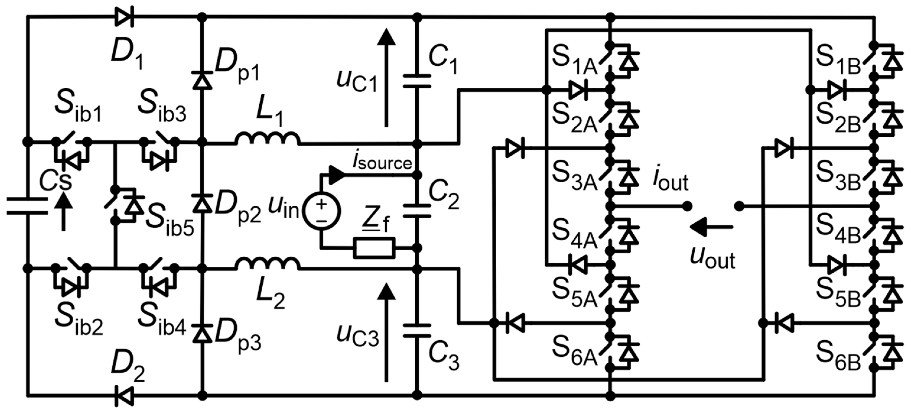
2. Concept of Operation of the System

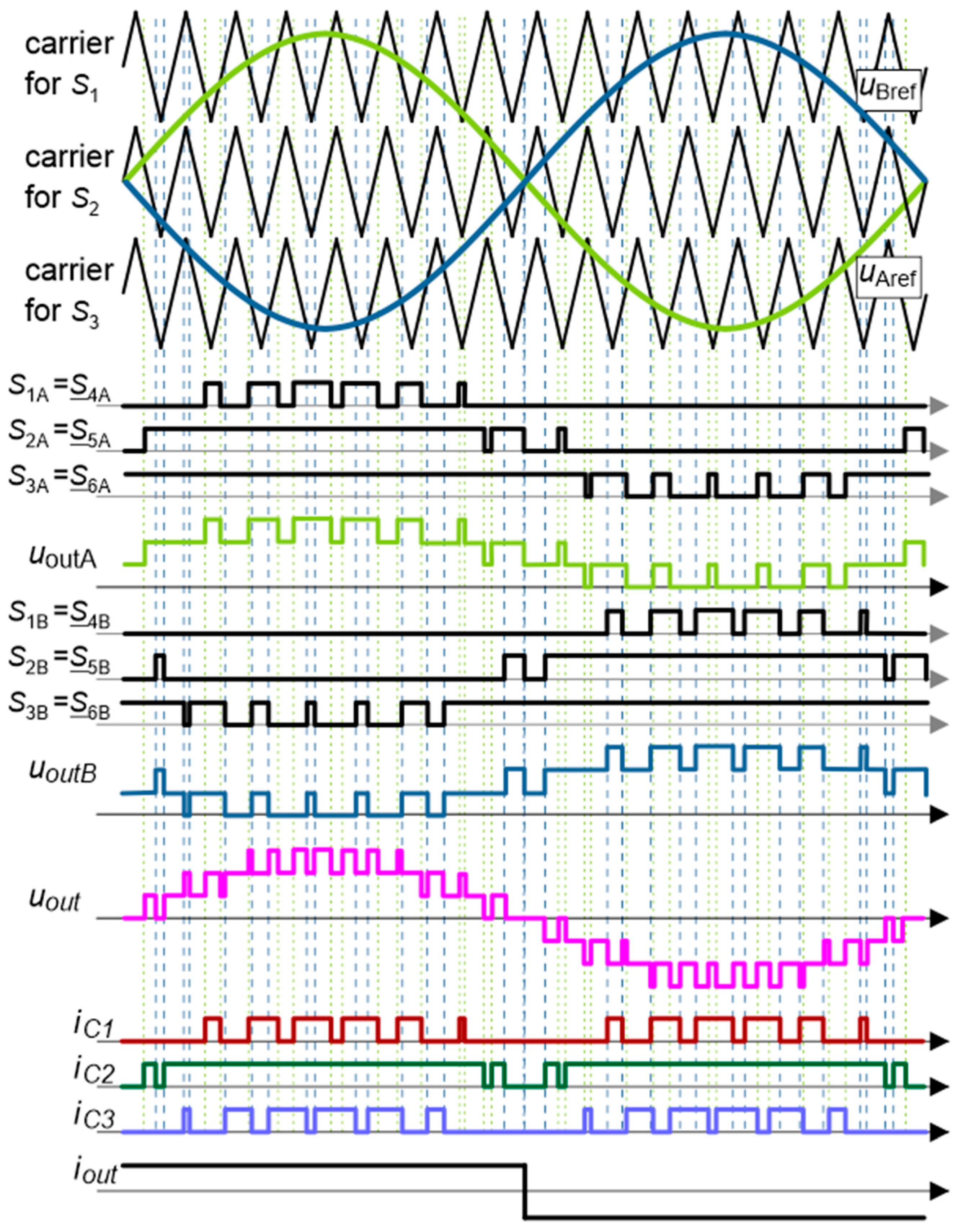
2.1. Modulation of the Inverter

The proposed system can utilize simple switching strategy based on the classic PD-PWM method (Figure 2). From the model of operation presented in Figure 2 it is seen that the discharge rate of the C2 capacitor is much larger than in the case of capacitors C1 and C3. This indicates that the PD-PWM may not be applicable for the NPC inverter with four-level legs (as in the analyzed case) because it leads to an unequal discharging of the DC-link capacitors. However, it is an advantage in the proposed system, since the C2 capacitor takes energy directly from a source. The other capacitors are supplied by the AIVB which also assures boosting of the input voltage and DC-link voltages balancing.
The AIVB (Figure 1 and Figure 3) charges the upper and lower DC-link capacitor (C1 and C3) from the source (connected to C2) with unity voltage gain. In ideal conditions, it leads to the state where uC1 = uC2 = uC3 = uin. The AIVB is based on SC resonant circuits with low volume resonant chokes (L1 and L2 = 3 uH in the demonstrated design). The resonant chokes limit the inrush current in the SC circuits and allows for oscillatory currents in ZCS (zero current switching) mode (Figure 3). More details related to selection of passive components are included in Section 2.2.2. The AIVB contains five switches which is significantly optimized in relation to the voltage balance circuits presented in [15,16].
The basic control principle of the AIVB assumes the use of switching states which charge the switched capacitor from the source and discharge to one of the DC-link capacitors C1 and C3 (Figure 3). It is conducted in the following order with the frequency fsw:
SwitchingOrder = {St1, St2, St1, St3, St1…},
The switching frequency of the AIVB (fsw) is aligned to the oscillation frequency of the resonant circuits:
f 01 = 1 2 π ( L 1 + L 2 ) C s   ( in   S t 1   state ) ,   f 02 = 1 2 π L n C s   ( in   S t 2 ,   S t 3 ) ,
The use of switching order (1) causes charging the C1 and C3 capacitors from the source (connected with the C2) when uC1 < uC2 and uC3 < uC2. It is performed in open loop control system.
To limit source current ripples, the source is separated by a filter Zf (Figure 1).

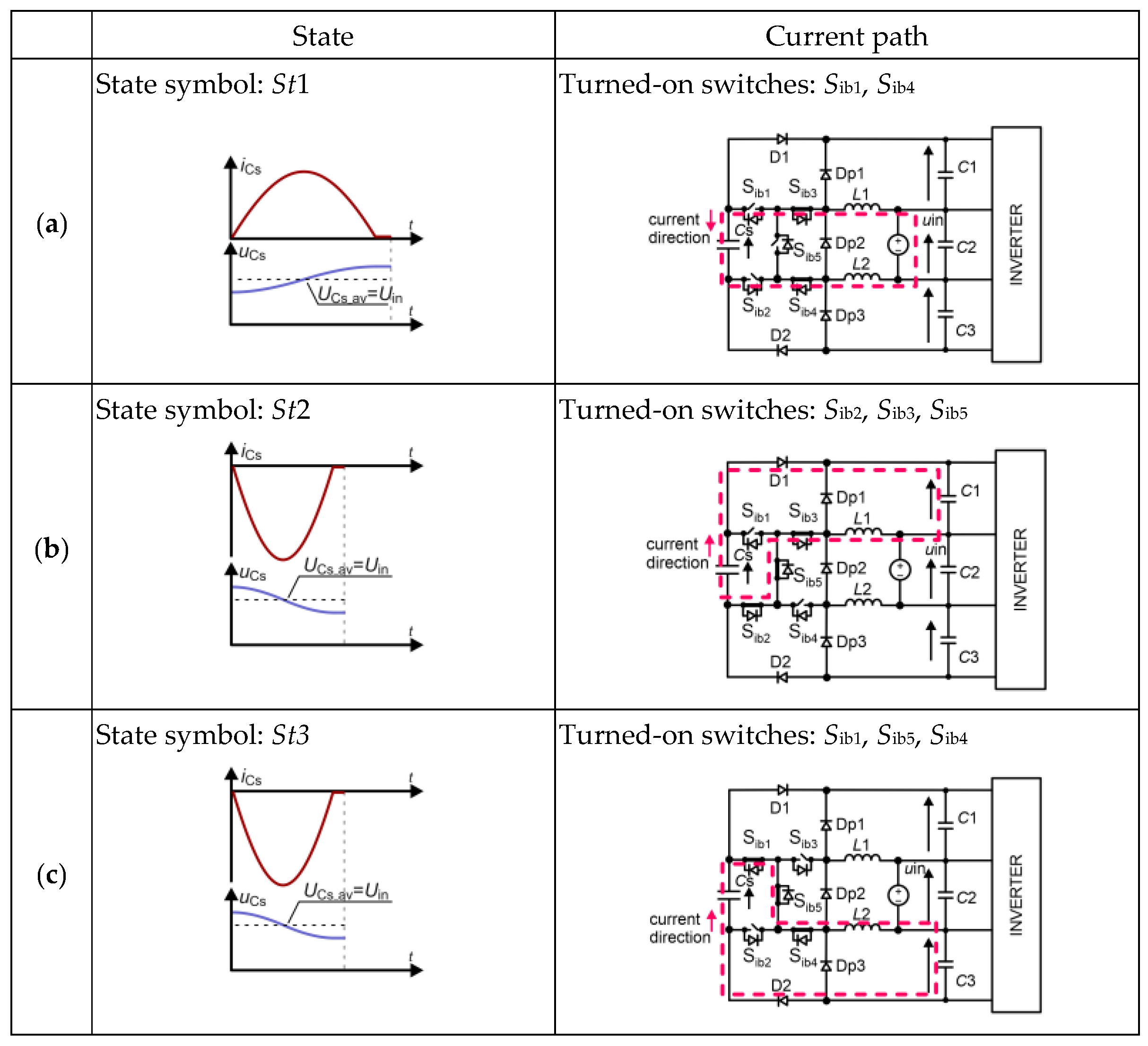
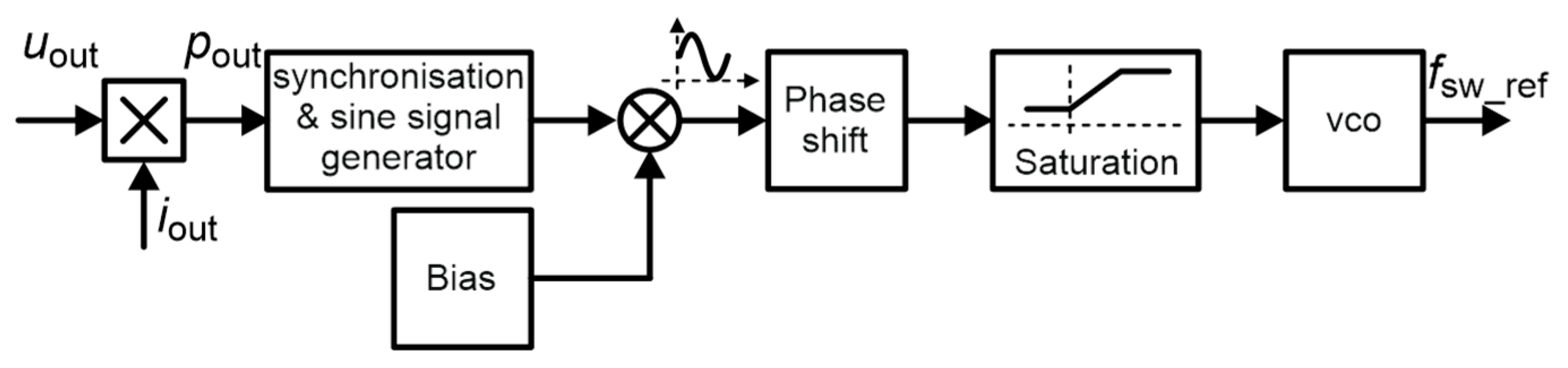
2.2. Realization of AIVB Control Concept

The control principle of the AIVB assumes operation in an open loop and the generation of switching states in an appropriate order (1). In the demonstrated case, the sequence of states (1) is achieved based on a state machine decoder. The period of each state is maintained by a counter which allows for a constant or variable switching frequency of the AIVB. The ratio of the time duration of the state St1 to states St2 and St3 is 58:42 in order to handle the difference in oscillation frequencies (2). Each of the states (St1, St2, and St3) have assigned transistors to be turned on. In case of operation with a variable switching frequency of the AIVB, the reference frequency is synchronized with the instantaneous output power (Figure 4). The described control method has been implemented in Matlab/Simulink for simulation and Cyclone III FPGA, DE0 development kit in experimental setup.

2.2.1. Reduction of the AC Component in the Source Voltage at the Double Frequency of the Output Voltage

The AIVB can reduce the AC double frequency component of the input current by controlling the amount of the energy transfer to C1 and C3. The function which determines the power of the AIVB should have an inverse character to the power on the output of the inverter (pout). When pout approaches its maximum, the charging rate of the C1 and C3 is the lowest. Therefore, the double frequency component is decreased in the source current and increases in C1 and C3 voltages where the instantaneous energy is stored. A concept of the AIVB power control will be presented in the sections with the simulation and experimental results (Section 3 and Section 4) in more details.
The AIVB operates with maximum power when the switched capacitor is fully recharged in each cycle. Its maximum voltage is 2Uin and the power is also a function of the switching frequency and the capacitance:
PAIVBmax = 0.5Cs(2Uin)2fsw,
From the relationship (3), it is seen that a variation of the switching frequency (fsw), in the range below the rated frequency, allows to control the AIVB’s power. With adequate synchronization of the output’s instantaneous power, this allows for a reduction in the double grid frequency from the source’s current. Figure 4 presents the concept of the closed control system for the power synchronization and double frequency reduction.

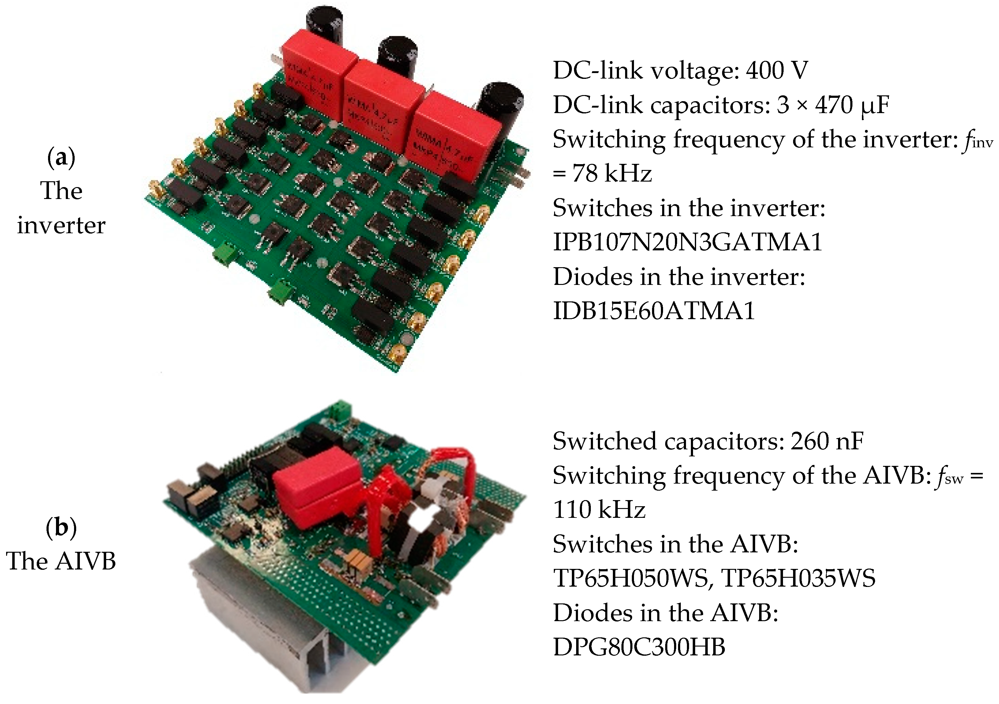
2.2.2. Selection of Components

The parameters of the switched capacitor circuits (Cs and also Ls) are dependent on the required power of the AIVB and the assumed switching frequency (which affects switching losses). The balancer can take the energy from the source with P = Pmax whilst C1 and C3 capacitors can be charged with the maximum power P1,3 = 0.5 PAIVBmax. From the principle of operation of the inverter the C1 and C3 DC-link capacitors transfers only part of the energy available on the AC side (on the basis of Figure 5):
P(C1 and C3)max = (0.63·ma − 3.2)Pinvmax,
where: ma is the modulation index of the inverter.
Considering the target control of the system, the C1 and C3 capacitor will store nearly the entire AC energy which allows for very low ripples in the DC source’s current (adequate results will be presented in the Section 3 and Section 4). For the average output power Pout = 1000 W, the AC energy in a half period is obtained as an integral of the AC output power:
poutAC = 1000 sin(618 t) ⇒ WAC = 1000∙(1/618)∙2 = 3.24 J,
To store half of the total AC energy, the C1 or C3 capacitor should have the following capacitance:
C1 = 2∙(WAC/2)/(UC1max2UC1min2),
For the demonstration purpose, the following range of DC-link capacitor C1 and C3 voltage is assumed: UC1max = 133 V and UC1min = 100 V. In such a case, the relationship (6) allows to calculate the capacitance C1 = C3 = 421 μF. In further tests, the DC-link capacitances are 500 μF for simulations (Table 1) and 470 μF for experiments (Section 4). Such values of capacitances allow to clearly demonstrate phenomenon of AC energy storage. To operate with lower voltage ripples, larger capacitance of C1 and C2 DC-link capacitor banks is required, according to the relationship (6).
Capacitance of the C2 capacitor should be selected to meet the assumed requirements for the source’s current filter design.
To control the AC output power, the power of the balancer, expressed by the relationship (3), should comply with the condition:
PAIVBmax ≥ 0.5P(C1 and C3)max,
Based on (3), for Uin = 133 V, fsw = 110 kHz, and Cs = 320 = nF the AIVB’s maximum power is PAIVBmax = 1245 W, which satisfies the requirements of the demonstrated design with not significant oversizing (for experiments Cs = 260 = nF, PAIVBmax = 1011 W). To operate in ZCS, the AIVB utilizes low volume resonant chokes (L1, L2) which makes the switched capacitor current oscillatory. Selection of L1 and L2 inductance is determined by earlier selected parameters of the AIVB such as its rated power, switching frequency, and switched capacitance. The frequency of natural oscillation in the circuit composed of the Cs and resonant chokes (L1, L2) should be higher than the switching frequency. The chokes (L1, L2) of 3μH satisfy this requirement, giving f0 = 115 kHz when the circuit contains two chokes as in Figure 3a, and f0 = 162 kHz when the circuit contains one choke as in Figure 3b,c.
In the simpler case of control, the AIVB boosts the voltage of C2 capacitor. Voltages on C1 or C3 reflect the uC2 voltage and selection of their capacitance should assume high frequency ripples reduction.

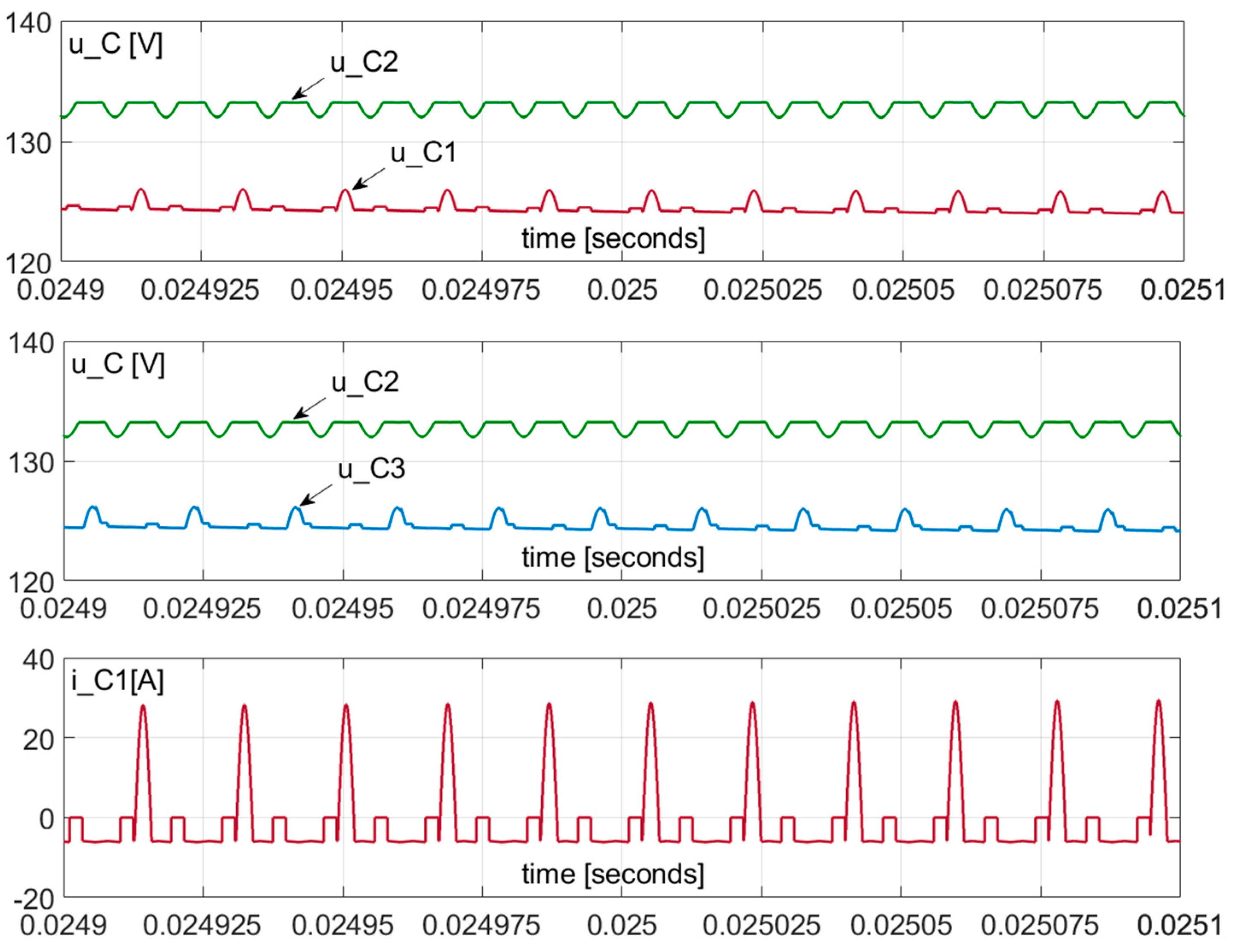
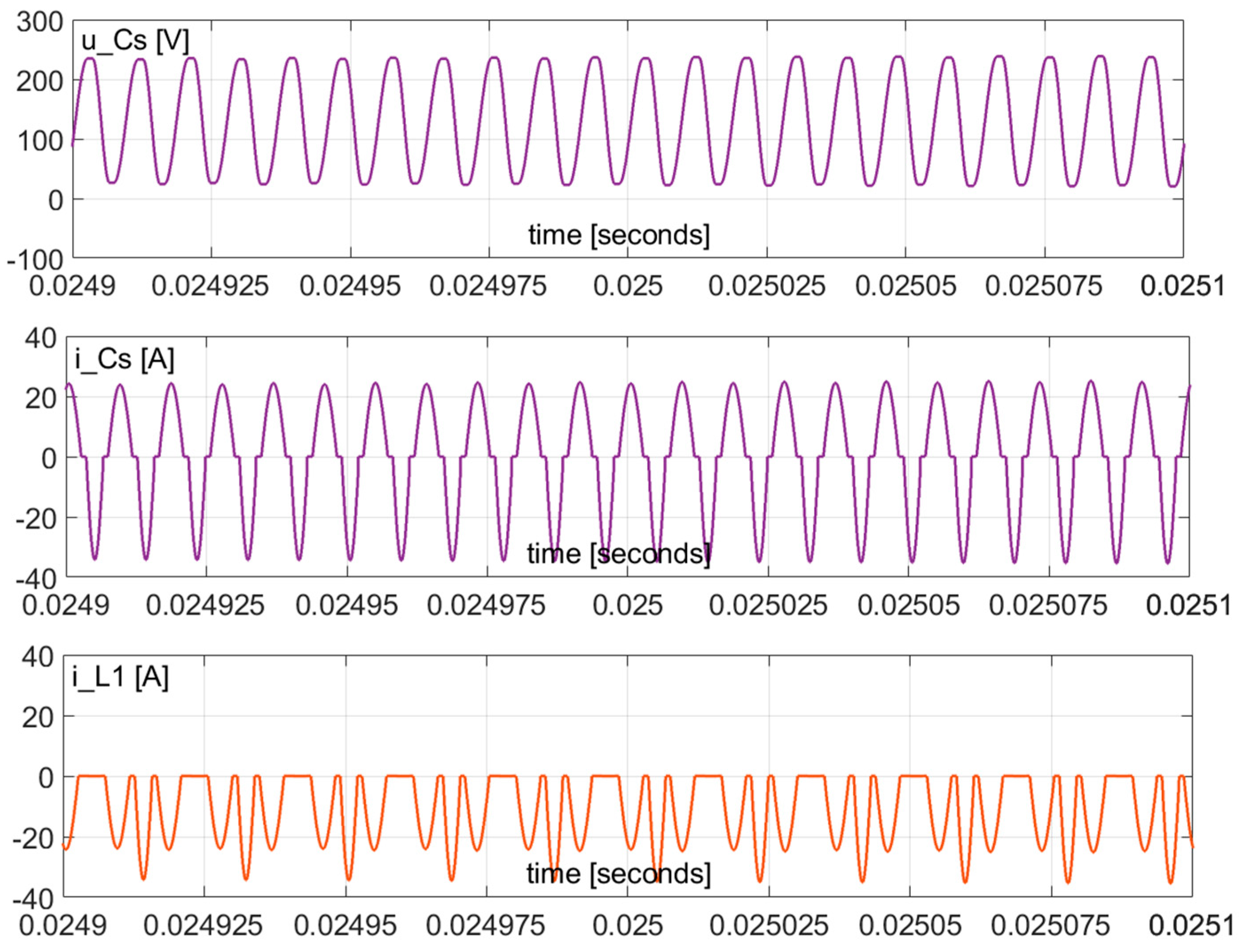
3. Simulation Results

The results of the simulation presented in this section verify the concept of the inverter’s operation, the AIVB and the complete system. The research was conducted with the use of Matlab/Simulink software with the parameters presented in Table 1.

3.1. Power of DC-Link Capacitors in Seven-Level HB Inverter

To demonstrate the operation of the inverter and energy required for particular DC-link capacitors, the inverter with three input voltage sources were analyzed (Figure 5a). Figure 6 presents the waveforms of the operation of the inverter with three input voltage sources and PD PWM. The results shown in Figure 6 confirms that the load of the internal source, connected to C2 capacitor, is the highest. For the lower modulation index of ma = Uref_max/Ucarrier_max, the discharging rate of C2 capacitor becomes significantly higher than the discharging rate of the C1 (or C3) capacitor. For ma = 0.6, 67% of power comes from the C2 capacitor and for ma = 1, PC2/Pout it is over 0.41 (Figure 5b). These results show that the use of the classic PD modulation is favorable when the source is connected to the middle DC-link capacitor (C2). The energy required for the maintenance of voltage on the C1 and C3 capacitors is transferred by the AIVB. In the analyzed case of operation of the inverter (UDC = 400 V, Uout = 230 V) the auxiliary circuit AIVB transfers approximately only 50% of power to the C1 and C3 capacitors.

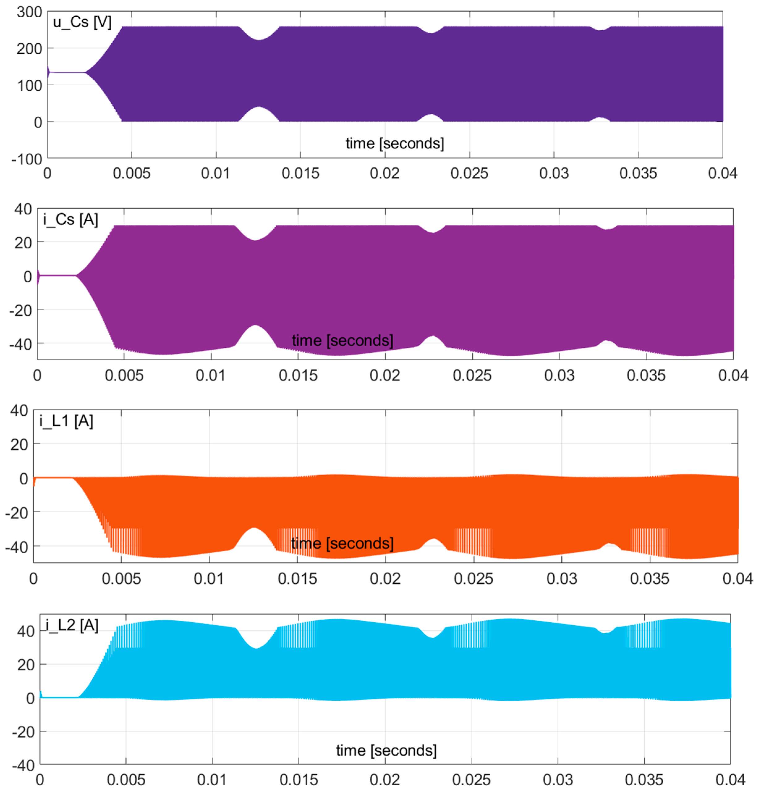
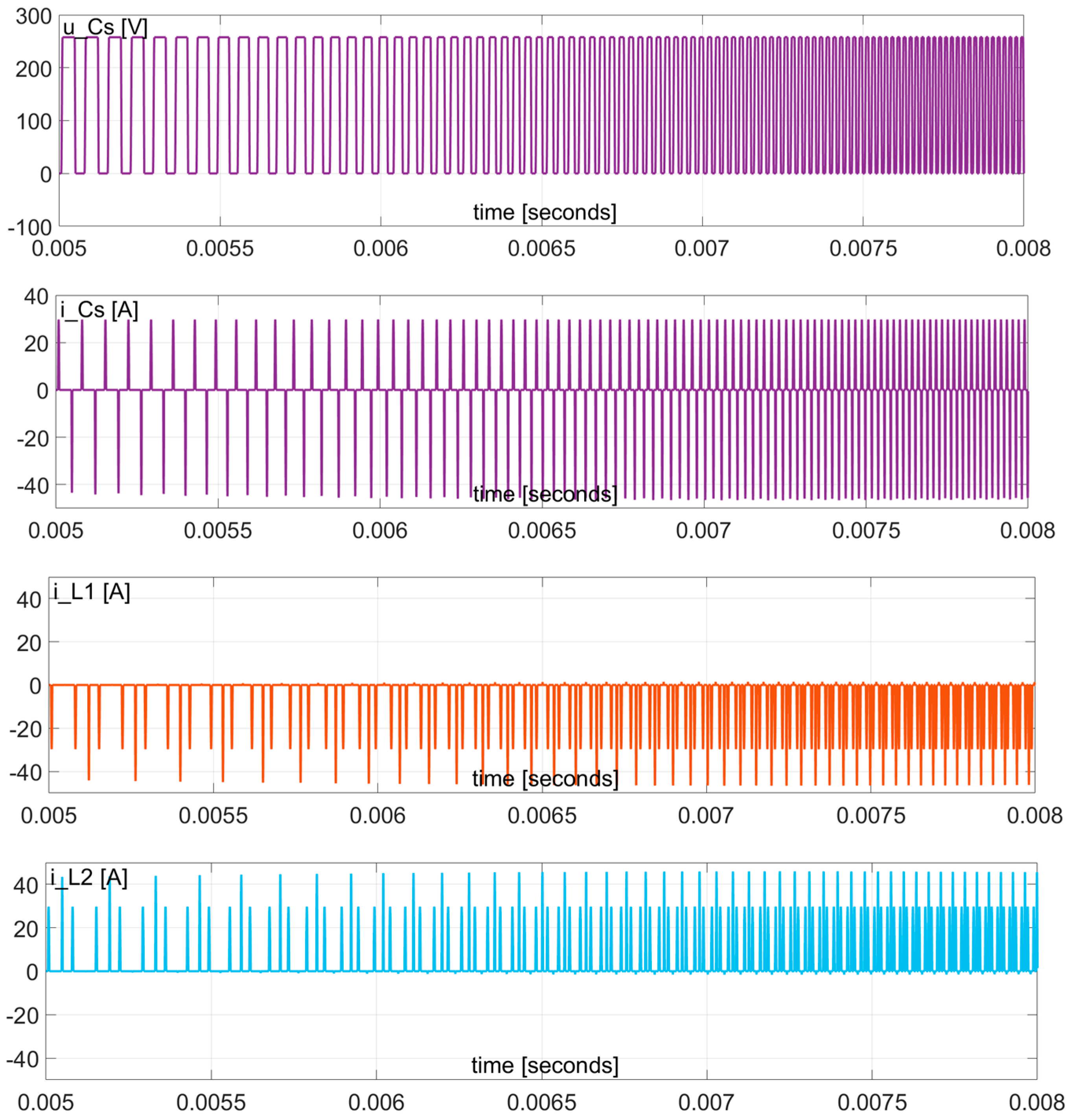
3.2. The Converter with the AIVB Operating in the Continuous Mode with Fixed Frequency

The basic control method of the AIVB assumes the use of a repetitive sequence of states defined by the SwitchingOrder (1) series. According to (1) the AIVB is constantly switching without additional control. As the voltage on C1 or C3 capacitor is below the source voltage the capacitor is charged. Figure 7, Figure 8, Figure 9 and Figure 10 present simulation results of this case. These results demonstrate that the AIVB maintains the voltages on C1 and C3 DC-link capacitors. Figure 7 and Figure 9 show the instantaneous increase of power of the AIVB when the output voltage is modulated on higher levels.
The AIVB’s operation is presented in Figure 8 and Figure 10 with details (25 μs/div). It is a fragment of the waveforms when the load of the AIVB is the highest. Resonant charging and discharging of the DC-link capacitors with the use of a switched capacitor is clearly visible. In every switching period the C2 capacitor is discharged and the C1 or C3 capacitor is charged. The frequency of pulses of the current in the C2 capacitor is two times higher than in the C1 and C3 (Figure 8).
In the proposed test case, the switched capacitor is not fully discharged in the switching period (Figure 9 and Figure 10). Even at the maximum instantaneous output power the AIVB operates below its maximum available power (which was calculated in Section 2.2). Frequency voltage ripples of 100 Hz are seen on C1 and C2 capacitors due to voltage drops on parasitic resistances and diodes of the balancer. Assuming 100 mΩ total parasitic resistance of a circuit during the stage of the Cs discharging, the resistive voltage drop is 3.5 V at the maximum current 35A. Considering the resistive voltage drop which occurs during Cs charging as well as forward voltage on diodes, the total maximum voltage drop between the input port (C2) and the output port (C1 or C3) of the balancer can be estimated at 9 V which corresponds with results presented in Figure 7 and Figure 11. The low frequency ripples in DC-link C1 and C3 capacitors can be minimized by reduction of stray resistance, Rds(on) of transistors and voltage drops on diodes of the balancer.

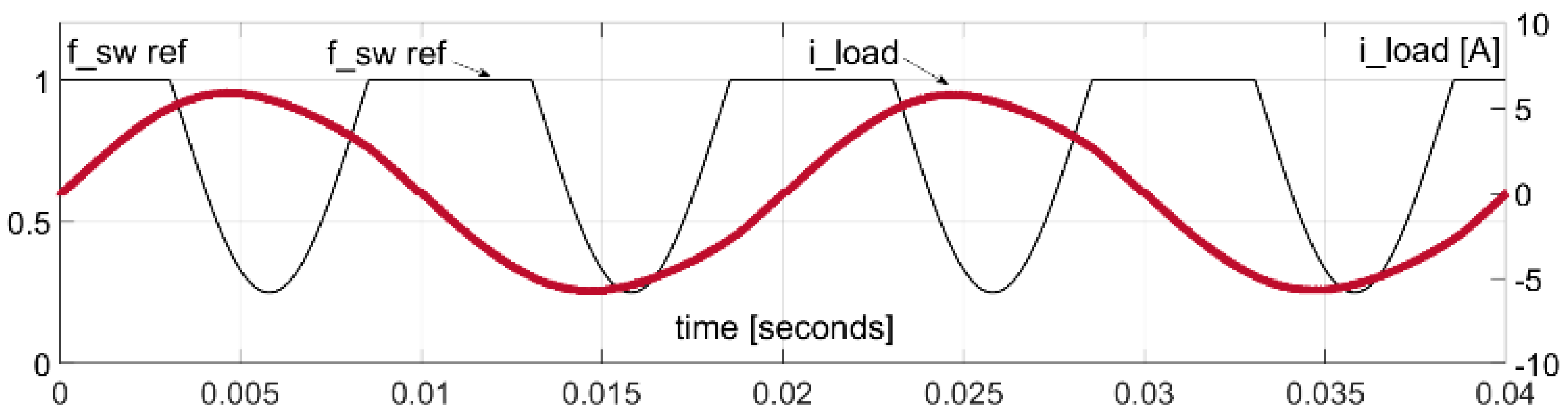
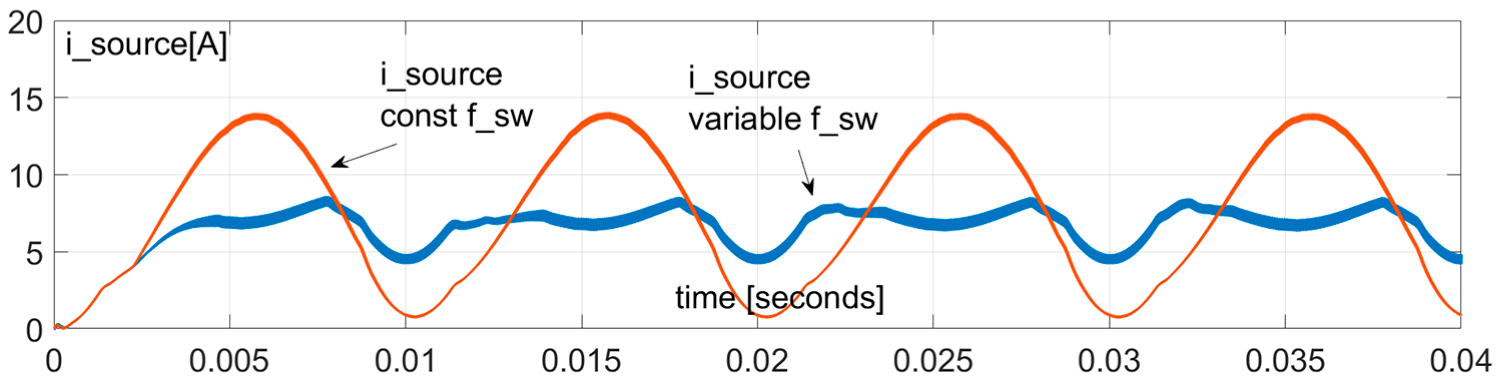
3.3. Double Frequency Reduction in the Source Current by Control of the AIVB Power

As can be observed in Figure 7, the DC source current (isource) has an AC component at double frequency of the output voltage. In order to reduce this component from the source’s current, a method for additional control of the AIVB’s operation was introduced. The concept is based on the switching frequency of the AIVB variations (fsw = var) which affects the amount of energy transferred from the C2 to C1 and C3 DC-link capacitors. The method of the reference generation for the switching frequency of the AIVB (fsw_ref) is based on the concept presented in Figure 4. It is composed of sinusoidal signal with amplitude of 0.65 positive biased by 0.1, limited to maximum value of 1 and phase shifted by 2π/3 [rad] (Figure 12). Such a reference for the AIVB’s control has been developed by the simulation study where a sweep of bias and phase shift has been performed, seeking the best double frequency reduction.
At the peak input current of the DC source, the switching frequency of the AIVB reaches its minimum and the rate of energy transferred from the DC source to the C1 and C2 capacitors is minimal. Meanwhile, the inverter output power decreases and, thus, the current drawn from the DC source, C1, and C2 are charged with a higher energy ratio. Figure 13, Figure 14, Figure 15, Figure 16 and Figure 17 present simulation results in the case when the AIVB operates with variable frequency. The results presented in Figure 7 and Figure 13 show that when the AIVB operates with variable frequency the AC component of the input current is considerably decreased whilst the variation of voltage on the C1 and C3 DC-link capacitor increases.
These DC-link capacitors store the instantaneous energy, and the load of the DC source is more even. The load of the AIVB is better distributed in a time period of the inverter voltage when its power is controlled (comparison of Figure 9 and Figure 14). Figure 15 and Figure 16 present a shorter time span (500 µs/div) when the AIVB switching frequency (fsw) varies from its minimum to maximum. As observed, the switched capacitor is fully discharged in every switching period thus it is utilized with the maximum power.
The overall energy transfer rate between the DC-link capacitor is controlled by the variation of the switching frequency. The method’s effectiveness for double frequency reduction in the input current is seen when comparing of the results achieved in the two analyzed cases of AIVB operation presented in Figure 17. When the source voltage is constant the significant reduction of double-frequency ripples from the source’s current confirms the effectiveness of the proposed active power decoupling method.

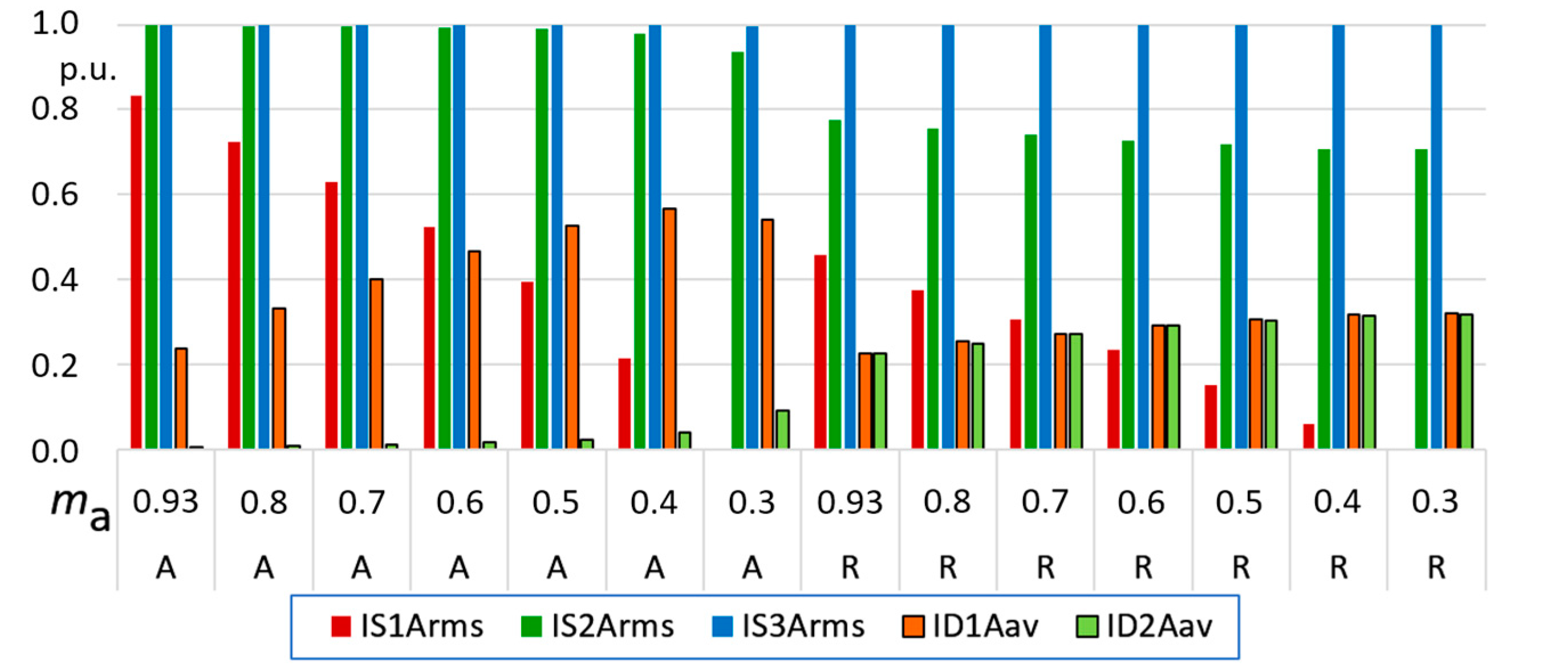
3.4. Switch Load by Currents of Converters and Conduction lLosses

To estimate conduction losses and the thermal design in the converter, the switches and diodes load should be evaluated. In the AIVB, the currents’ load of switches can be simply compared based on its operation principle. The use of the switching order (1) creates a slight inequality of conduction among the switches (Table 2). The value of the current is equal in switches Sib1Sib4. They conduct the current during the three of four subperiods of (1) whilst the switch Sib5 during the two of four. It creates nearly equal heat distribution from the switches. The lowest current value is seen in diodes D1 and D2.
The current stress of the inverter switches depends here on the modulation index (ma) and the output power value as well as its character. Additionally, the number of switching operations of devices varies versus ma, Pout, and Qout. Figure 18 presents the simulation results of such comparison and the chart with the dependency of the current load of switches and diodes versus the modulation index and power. From these results (Figure 18) it is seen that for operation with the active power and high ma, the current value of switches is nearly the same in all devices and the inequality of current stress is seen among the diodes. Under the determined range of ma, Pout, and Qout, the thermal design requirements can be estimated.
From Figure 3 it is also seen that voltage stress on the AIVB’s switches reaches uCSmax (≤Uin). The voltage stress of semiconductor devices in the inverter is equal to the Uin (which 1/3 of the total DC-link voltage).

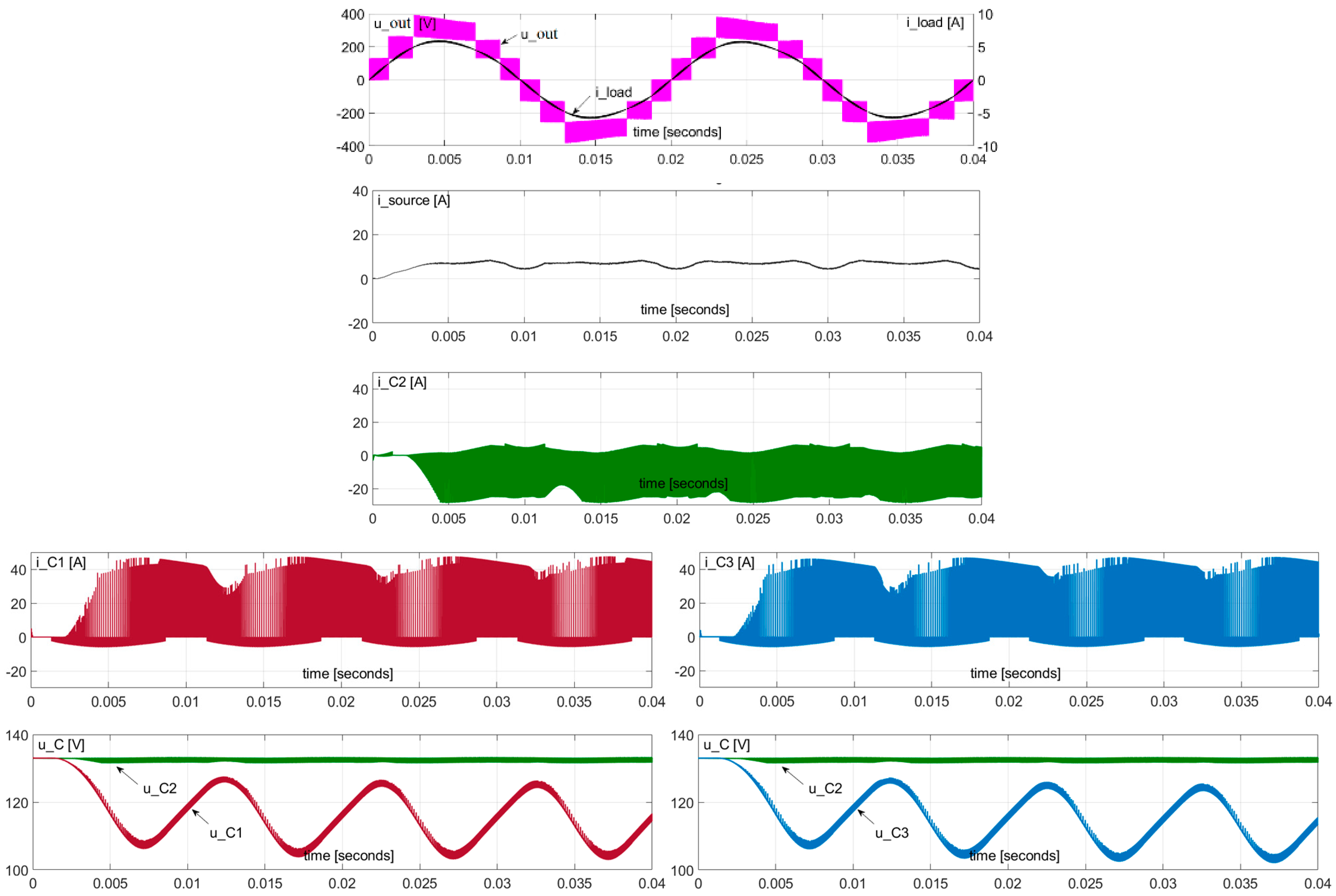
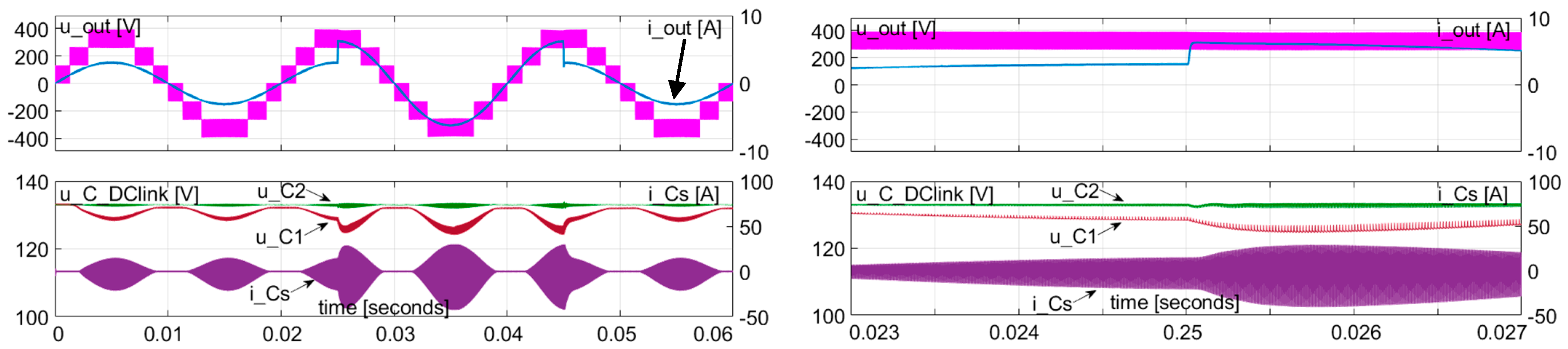
3.5. Step Change of Load

The AIVB does not regulate voltage in a closed loop control, but it operates with the unity voltage gain (UC3 = UC2 and UC1 = UC2). Its dynamics can be described as a first order system, which is demonstrated by the example simulation results presented in Figure 19 where the step changes of load occur on the AC side.

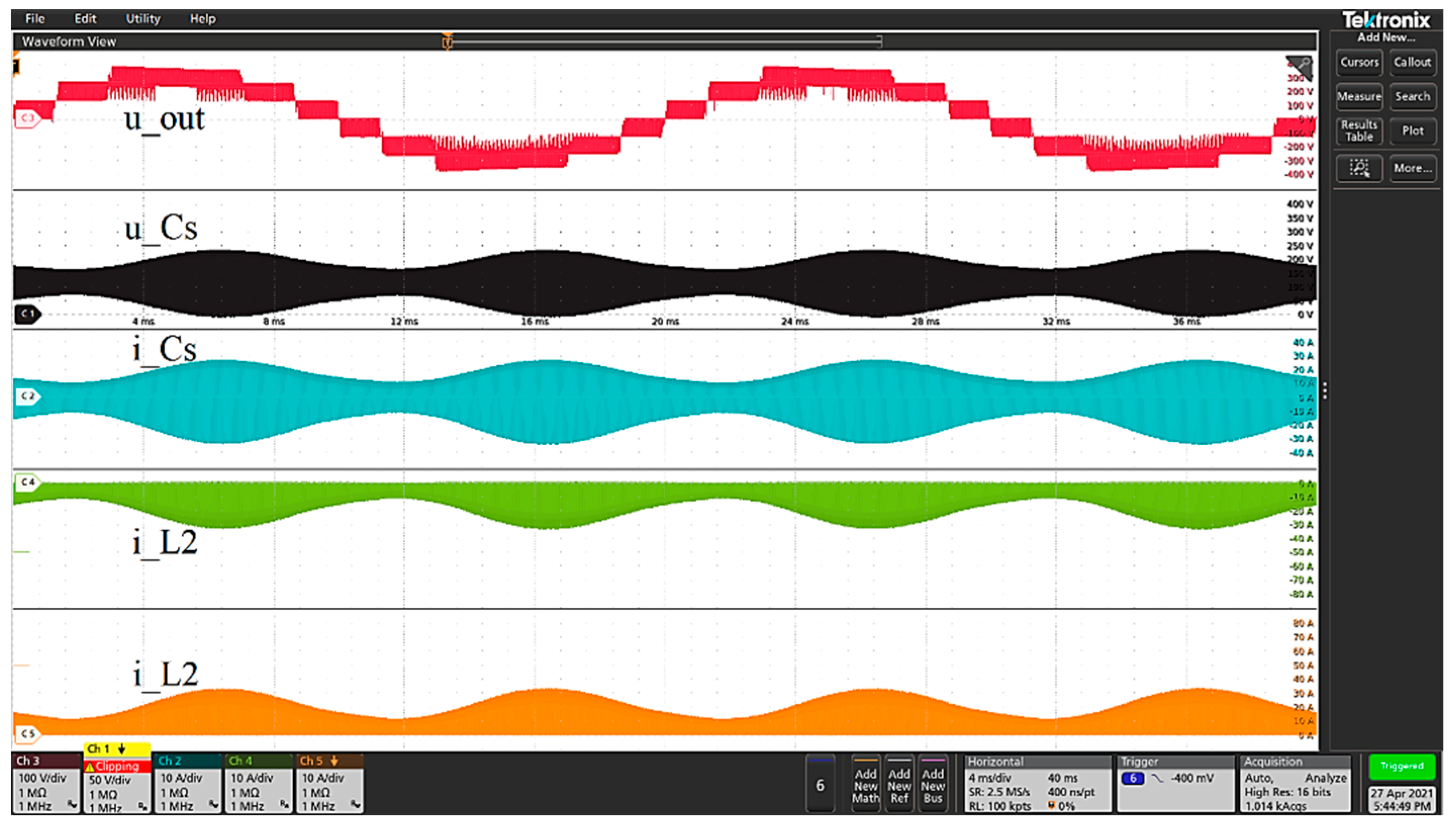
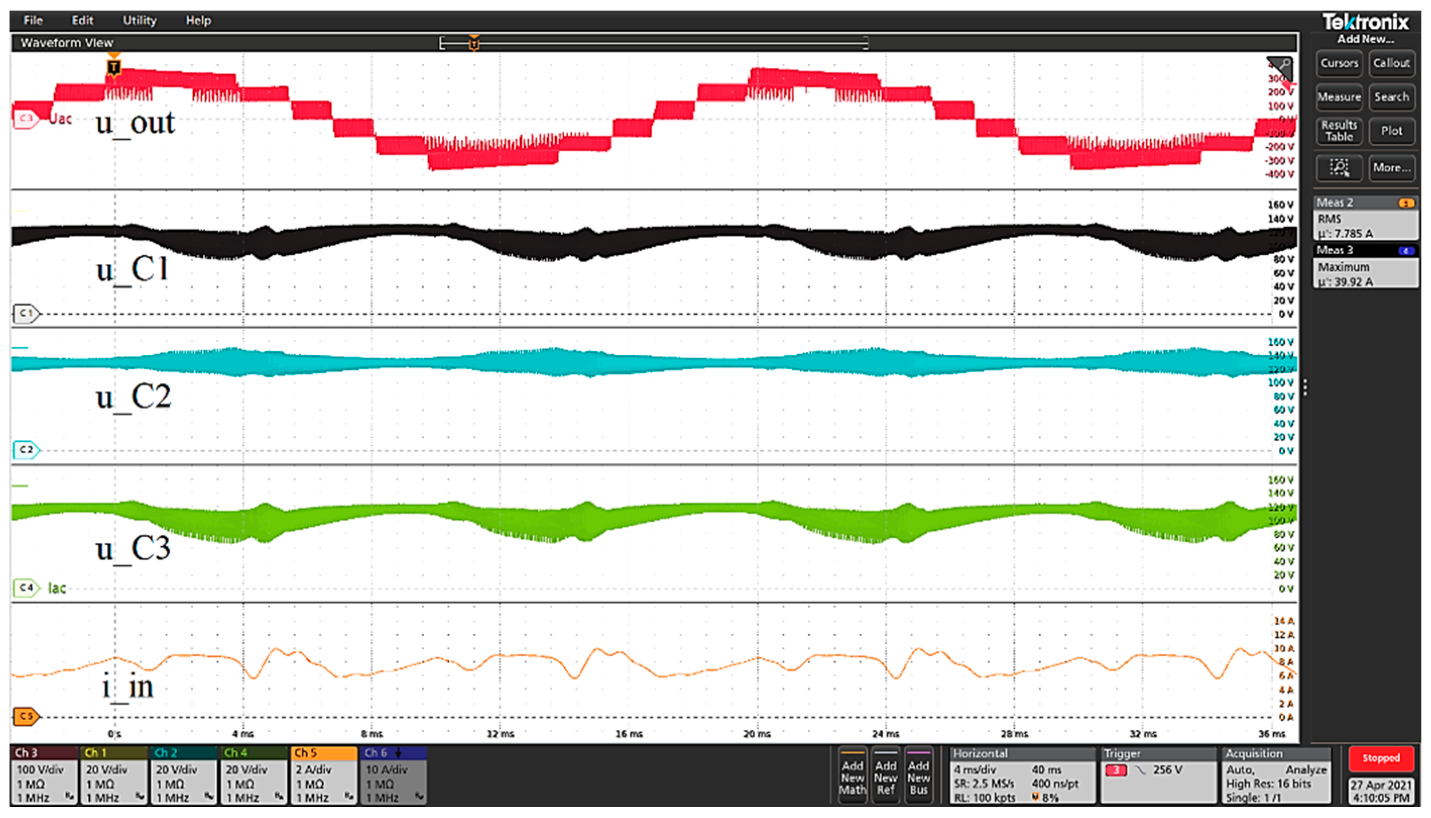
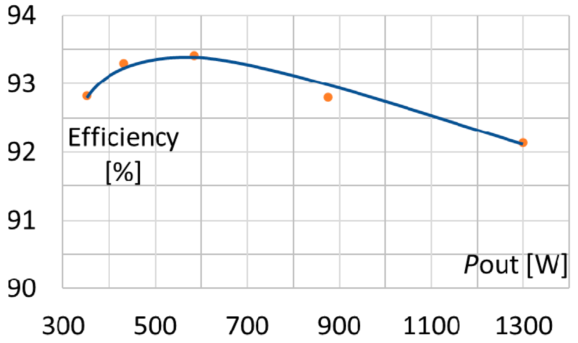
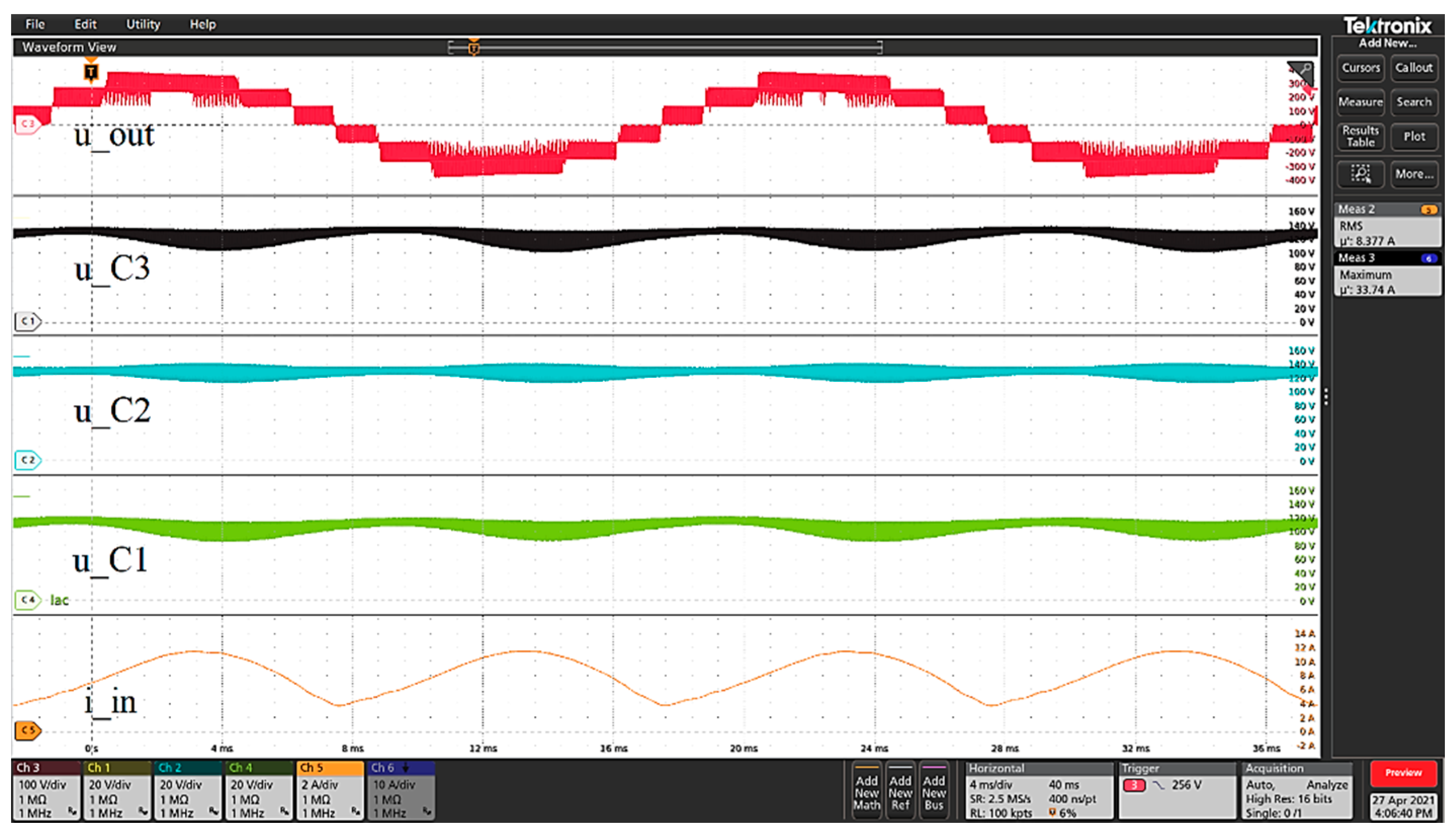
4. Experimental Results

The experimental tests were performed with the converters and setup described in Figure 20. The experiment was prepared to confirm the correctness of the concept of the system configuration and control. The system is composed of two converters and two methods of the input power control were verified as well. To implement the single-phase inverter at 400 V on DC-link, the MOSFET with VDS = 200 V and low on-state resistance were used. The AIVB was designed as a GaN based converter to minimize Coss losses, since operating in ZCS mode transistors of the AIVB are turned-on when their output capacitance is charged. A typical drain to source voltage VDSS = 650 V allows to avoid overvoltage failure in the tested AIVB circuit.

4.1. Operation of the Inverter with the PD-PWM Method and Three DC Sources

Using the setup configured according to Figure 5a, where the voltage on each DC-link capacitor is supplied by an independent DC power supply, the seven-level inverter with the PD-PWM was verified. Figure 21 presents the waveforms of the inverter operating with Pout = 982 and the measurements of particular input powers with the values: PC1 = 255 W, PC3 = 251 W, and PC2 = 521 W. This means that over 50% of the power can be converted to the AC side directly from the source which is connected to the C2 (Figure 1) and 50% of energy will be converted by the boost stage in the system with the AIVB.

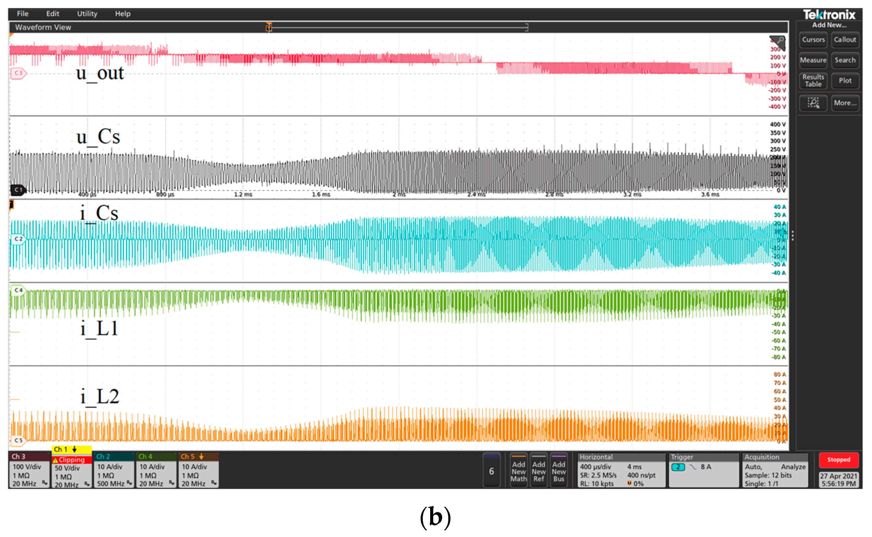
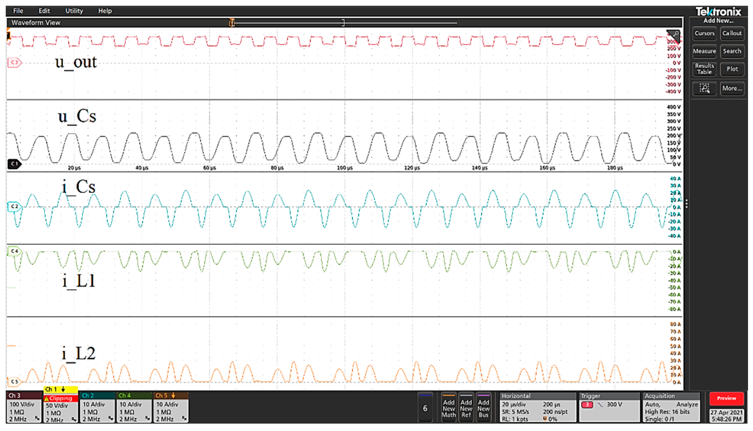
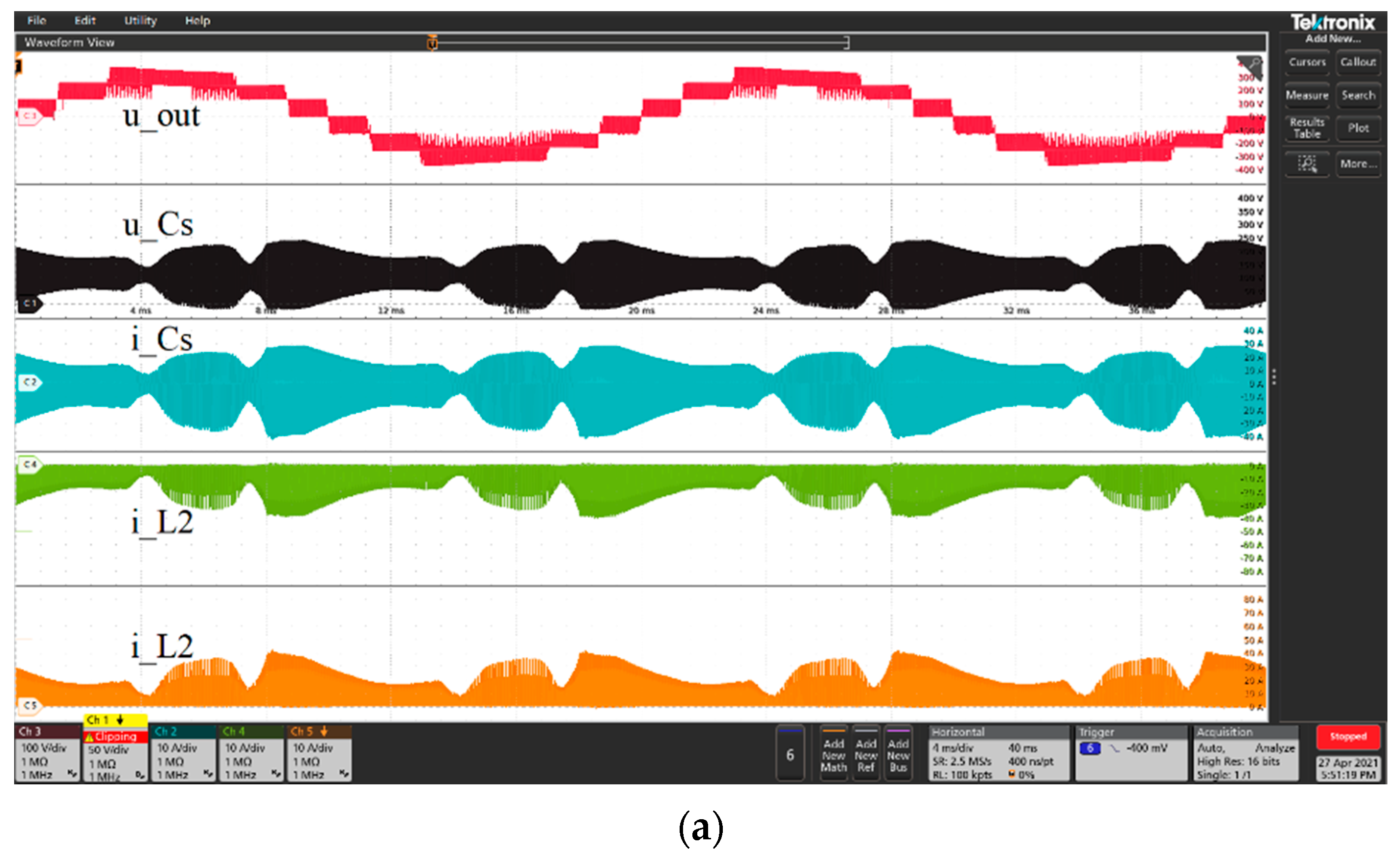
4.2. Operation of the AIVB

The operation of the AIVB is documented by the experimental waveforms presented in Figure 22, Figure 23, Figure 24, Figure 25 and Figure 26. The results illustrate that the converter operates exactly in accordance with the original concept. The switched capacitor is charged from the C2 DC-link capacitor in the circuit composed of two resonant inductors. It is further discharged to the upper and lower DC-link capacitors (C1 or C3) in a series connection with one of the resonant inductors.

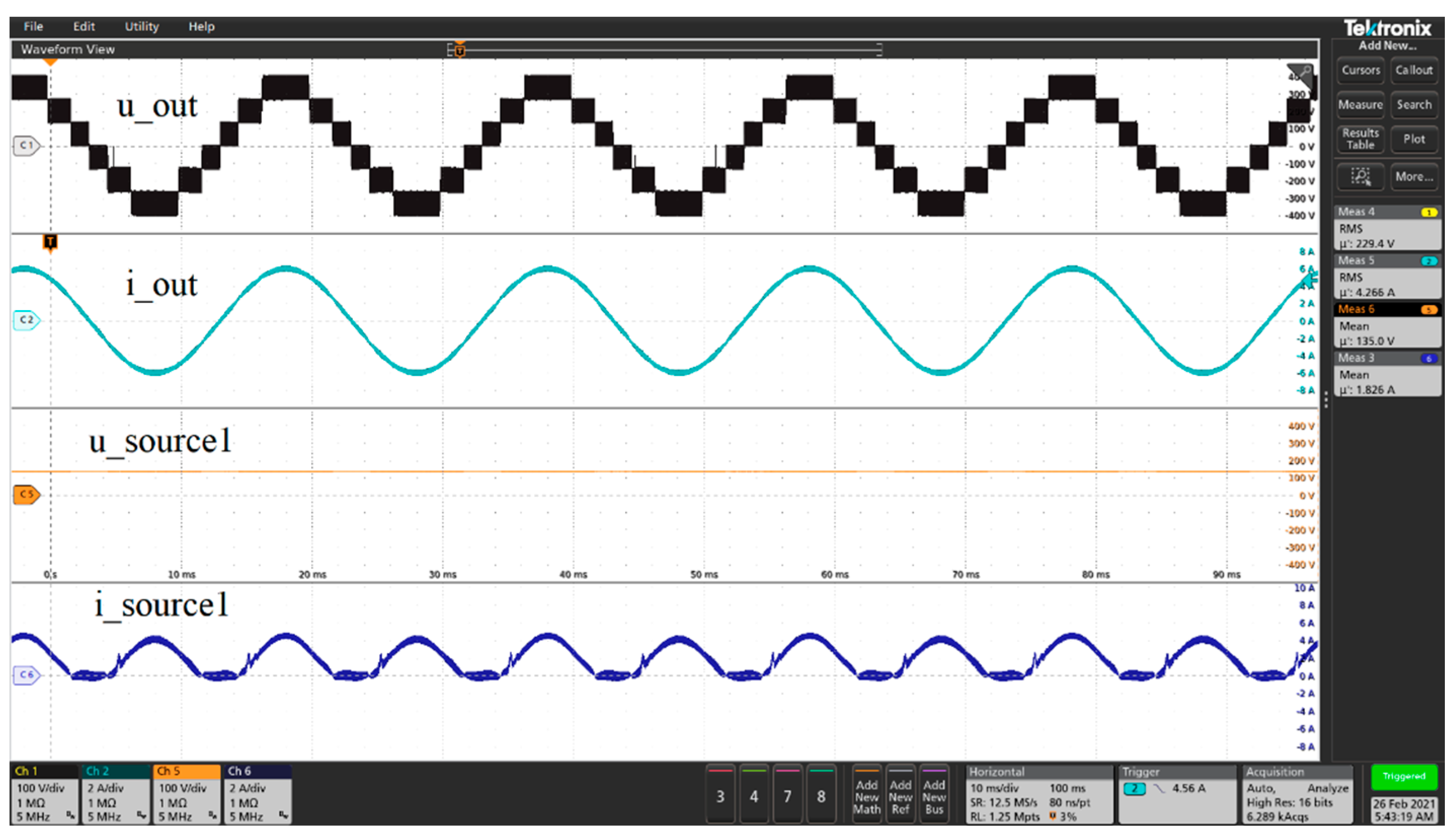
4.3. Operation of the Inverter with the AIVB Converter

In the analyzed system, the energy source is connected to the middle capacitor (C2) of the DC-link of the seven-level NPC bridge inverter (as Figure 1). The AIVB transfers the energy to other capacitors of the DC-link (C1 and C3). It assures the input voltage boosting and the DC-link voltage balancing. The operation of the AIVB is confirmed by the results presented in Figure 22. Figure 23 and Figure 24 demonstrate the operation of the whole system, where the AIVB is controlled according to the switching order defined by function (1) with a constant switching frequency. In this low complex method, the voltage on the DC-link capacitors is maintained correctly. Any measurements on the DC-link capacitors are not required. Power of the AIVB depends on the instantaneous power on the output of the inverter.
To reduce the 100 Hz component in the source current, power control can be implemented in the AIVB. The method is presented in Section 3.3 and it allows to control the power of the AIVB by variation of its switching frequency. Figure 25 and Figure 26 present the operation of the DC-AC system with the AIVB operation with variable frequency. These results show that the significant reduction of the 100 Hz component in the current of the DC-power supply connected with the C2 capacitor can be achieved by the control of the AIVB.
For the demonstrated implementation of the converter (Figure 20), the overall efficiency results are presented in Figure 27.

5. Comparison to Existing Solutions

The demonstrated results prove a versatile ability of the proposed front-end converter for the DC-link voltages management in the four-level NPC converter. The converter is finally compared to other topologies of auxiliary balancing circuits (Table 3). The comparison of the number and volume of components can be considered beneficial for the proposed circuit as it uses one 260 nF switched capacitor and low volume 3 µH resonant inductor.
Table 4 presents the comparison of the proposed converter with 7-level single phase inverter based on SC technique. An important benefit of the proposed converter, which is seen when compared to the other SC inverters, is its AC power decoupling ability. Furthermore, the presented AIVB front-end converter can be used in 3-phase NPC inverter with 4-level legs for voltage boosting and DC-link voltage balancing. It is also important that in some power converter topologies based on a pure switched capacitor concept, the problem of inrush currents exists and often makes the design challenging. Therefore, another positive quality of the proposed converter is the concept of resonant circuits in the front-end AIVB converter and recharging the switched capacitor by oscillatory currents.

6. Conclusions

In the proposed concept of the bridge inverter composed of four-level NPC legs and the active input voltage balancer (AIVB) in front, the three-fold boosting of the input voltage and the DC-link voltage balancing is achieved. It is favorable that the majority of energy can be transferred from the source to the AC side without DC-DC conversion, directly from the middle capacitor of the DC-link. The AIVB transfers only part of the energy among the DC-link capacitors.
This paper presents the novel concept of the system with an original input balancer (AIVB) and two methods of its control. In the first method the AIVB operates with a given sequence of switching states with a constant frequency. This simple strategy assures an adequate DC-link capacitor voltage balance and operation of the system. In the second proposed approach, the power of the AIVB is synchronized with the output power. It is a very favorable approach of a single-phase system as it allows for a decrease in the variable component in the DC source current at double frequency of the output voltage. The instantaneous power of the AIVB can be controlled by its switching frequency variation, to decrease when the output power increases.
The proposed system can be considered for single-phase photovoltaic systems. Typical functions required in such conversion systems, such as voltage boosting, AC power decoupling and DC-link voltage balancing, are assured by the proposed converter. The performed experiment shows that the 7-level inverter can operate at 400 V on the DC-link using MOSFET switches with VDS = 200 V and very low RDS(on).

Author Contributions

Conceptualization, R.S. and J.H.; methodology, R.S. and J.H.; software, R.S., J.H. and A.P.; validation, R.S., J.H. and A.P.; formal analysis, R.S.; investigation, R.S., J.H. and A.P.; resources, R.S. and J.H.; data curation, R.S. and J.H.; writing—original draft preparation, R.S. and J.H.; writing—review and editing, R.S. and J.H.; visualization, R.S. and J.H.; supervision, R.S.; project administration, R.S.; funding acquisition, R.S. All authors have read and agreed to the published version of the manuscript.

Funding

This research received no external funding.

Institutional Review Board Statement

Not applicable.

Informed Consent Statement

Not applicable.

Data Availability Statement

Not applicable.

Conflicts of Interest

The authors declare no conflict of interest. The funders had no role in the design of the study; in the collection, analyses, or interpretation of data; in the writing of the manuscript; or in the decision to publish the results.

References

  1. Rodriguez, J.; Bernet, S.; Steimer, P.K.; Lizama, I.E. A Survey on Neutral-Point-Clamped Inverters. IEEE Trans. Ind. Electron. 2010, 57, 2219–2230. [Google Scholar] [CrossRef]
  2. Nabae, A.; Takahashi, I.; Akagi, H. A New Neutral-Point-Clamped PWM Inverter. IEEE Trans. Ind. Appl. 1981, IA-17, 518–523. [Google Scholar] [CrossRef]
  3. Zhang, L.; Sun, K.; Feng, L.; Wu, H.; Xing, Y. A Family of Neutral Point Clamped Full-Bridge Topologies for Transformerless Photovoltaic Grid-Tied Inverters. IEEE Trans. Power Electron. 2013, 28, 730–739. [Google Scholar] [CrossRef]
  4. Trabelsi, M.; Vahedi, H.; Abu-Rub, H. Review on Single-DC-Source Multilevel Inverters: Topologies, Challenges, Industrial Applications, and Recommendations. IEEE Open J. Ind. Electron. Soc. 2021, 2, 112–127. [Google Scholar] [CrossRef]
  5. Khan, M.N.H.; Forouzesh, M.; Siwakoti, Y.P.; Li, L.; Kerekes, T.; Blaabjerg, F. Transformerless Inverter Topologies for Single-Phase Photovoltaic Systems: A Comparative Review. IEEE J. Emerg. Sel. Top. Power Electron. 2020, 8, 805–835. [Google Scholar] [CrossRef]
  6. Salem, A.; Van Khang, H.; Robbersmyr, K.G.; Norambuena, M.; Rodriguez, J. Voltage Source Multilevel Inverters with Reduced Device Count: Topological Review and Novel Comparative Factors. IEEE Trans. Power Electron. 2021, 36, 2720–2747. [Google Scholar] [CrossRef]
  7. Zhang, Z.; Zhang, J.; Shao, S.; Zhang, J. A High-Efficiency Single-Phase T-Type BCM Microinverter. IEEE Trans. Power Electron. 2019, 34, 984–995. [Google Scholar] [CrossRef]
  8. Khazraei, M.; Zupancic, D. Solar Inverter Design. The Race to Design High-Efficiency, High-Power-Density Inverters. Power Syst. Des. 2020, 5, 9–12. [Google Scholar]
  9. Stala, R. Natural DC-link voltage balance in a single-phase NPC inverter with four-level legs and novel modulation method. IET Power Electron. 2020, 13, 3764–3776. [Google Scholar] [CrossRef]
  10. Strzelecki, R.; Szczepankowski, P.; Strzelecka, N. Four level diode-clamped back-to-back converter with active DC link voltage control. In Proceedings of the 2013 International Conference-Workshop Compatibility and Power Electronics, Ljubljana, Slovenia, 5–7 June 2013; pp. 182–187. [Google Scholar] [CrossRef]
  11. Shukla, A.; Ghosh, A.; Joshi, A. Flying-Capacitor-Based Chopper Circuit for DC Capacitor Voltage Balancing in Diode-Clamped Multilevel Inverter. IEEE Trans. Ind. Electron. 2010, 57, 2249–2261. [Google Scholar] [CrossRef] [Green Version]
  12. Cui, D.; Ge, Q. A Novel Hybrid Voltage Balance Method for Five-Level Diode-Clamped Converters. IEEE Trans. Ind. Electron. 2018, 65, 6020–6031. [Google Scholar] [CrossRef]
  13. Zhao, J.; Han, Y.; He, X.; Tan, C.; Cheng, J.; Zhao, R. Multilevel Circuit Topologies Based on the Switched-Capacitor Converter and Diode-Clamped Converter. IEEE Trans. Power Electron. 2011, 26, 2127–2136. [Google Scholar] [CrossRef]
  14. Shu, Z.; He, X.; Wang, Z.; Qiu, D.; Jing, Y. Voltage Balancing Approaches for Diode-Clamped Multilevel Converters Using Auxiliary Capacitor-Based Circuits. IEEE Trans. Power Electron. 2013, 28, 2111–2124. [Google Scholar] [CrossRef]
  15. Hachlowski, J.; Stala, R. DC-link Voltage Balancing Converter with Resonant Switched-Capacitor Circuit for Four-Level and Six-Level NPC Inverter. In Proceedings of the 2019 21st European Conference on Power Electronics and Applications (EPE 19 ECCE Europe), Genova, Italy, 3–5 September 2019. [Google Scholar] [CrossRef]
  16. Hachlowski, J.; Stala, R. A Novel Converter for Voltage Balance in A Series Connected Capacitors And Batteries. Power Electron. Drives 2018, 3, 65–74. [Google Scholar] [CrossRef] [Green Version]
  17. Taghvaie, A.; Haque, M.E.; Saha, S.; Mahmud, M.A. A New Step-Up Switched-Capacitor Voltage Balancing Converter for NPC Multilevel Inverter-Based Solar PV System. IEEE Access 2020, 8, 83940–83952. [Google Scholar] [CrossRef]
  18. Shimizu, T.; Koizumi, H. Modularized chain structure of switched capacitor for cell voltage equalizer with T-connected bi-directional switch. In Proceedings of the 2016 IEEE International Symposium on Circuits and Systems (ISCAS), Montreal, QC, Canada, 22–25 May 2016; pp. 1194–1197. [Google Scholar] [CrossRef]
  19. Liu, K.; Yang, Z.; Tang, X.; Cao, W. Automotive Battery Equalizers Based on Joint Switched-Capacitor and Buck-Boost Converters. IEEE Trans. Veh. Technol. 2020, 69, 12716–12724. [Google Scholar] [CrossRef]
  20. Pereda, J.; Dixon, J. High-Frequency Link: A Solution for Using Only One DC Source in Asymmetric Cascaded Multilevel Inverters. IEEE Trans. Ind. Electron. 2011, 58, 3884–3892. [Google Scholar] [CrossRef]
  21. Singh, J.; Dahiya, R.; Lalit Mohan, S. Recent research on transformer based single DC source multilevel inverter: A review. Renew. Sustain. Energy Rev. 2018, 82, 3207–3224. [Google Scholar] [CrossRef]
  22. Sun, X.; Wang, B.; Zhou, Y.; Wang, W.; Du, H.; Lu, Z. A Single DC Source Cascaded Seven-Level Inverter Integrating Switched-Capacitor Techniques. IEEE Trans. Ind. Electron. 2016, 63, 7184–7194. [Google Scholar] [CrossRef]
  23. Gautam, A.R.; Fulwani, D.M.; Makineni, R.R.; Rathore, A.K.; Singh, D. Control Strategies and Power Decoupling Topologies to Mitigate 2ω-Ripple in Single-Phase Inverters: A Review and Open Challenges. IEEE Access 2020, 8, 147533–147559. [Google Scholar] [CrossRef]
  24. Zhang, Y.; Xiong, J.; He, P.; Wang, S. Review of power decoupling methods for micro-inverters used in PV systems. Chin. J. Electr. Eng. 2018, 4, 26–32. [Google Scholar] [CrossRef]
  25. Vitorino, M.A.; Alves, L.F.S.; Wang, R.; de Rossiter Corrêa, M.B. Low-Frequency Power Decoupling in Single-Phase Applications: A Comprehensive Overview. IEEE Trans. Power Electron. 2017, 32, 2892–2912. [Google Scholar] [CrossRef]
  26. He, L.; Cheng, C. A Bridge Modular Switched-Capacitor-Based Multilevel Inverter with Optimized SPWM Control Method and Enhanced Power-Decoupling Ability. IEEE Trans. Ind. Electron. 2018, 65, 6140–6149. [Google Scholar] [CrossRef]
  27. Omomo, A.; Itoh, J.; Kusaka, K.; Takaoka, N.; Le, H.N. T-type NPC Inverter with Active Power Decoupling Method using Discontinuous Current Mode for Micro-Inverter. In Proceedings of the 2018 7th International Conference on Renewable Energy Research and Appl. (ICRERA), Paris, France, 14–17 October 2018; pp. 1147–1152. [Google Scholar] [CrossRef]
  28. Kumari, M.; Siddique, M.D.; Sarwar, A.; Tariq, M.; Mekhilef, S.; Iqbal, A. Recent trends and review on switched-capacitor-based single-stage boost multilevel inverter. Int. Trans. Elec. Energy Syst. 2021, 31, e12730. [Google Scholar] [CrossRef]
  29. Siddique, M.D.; Mekhilef, S.; Shah, N.M.; Ali, J.S.M.; Blaabjerg, F. A New Switched Capacitor 7L Inverter With Triple Voltage Gain and Low Voltage Stress. IEEE Trans. Circuits Syst. II Express Briefs 2020, 67, 1294–1298. [Google Scholar] [CrossRef]
  30. Sathik, M.J.; Sandeep, N.; Siddique, M.D.; Almakhles, D.; Mekhilef, S. Compact Seven-Level Boost Type Inverter Topology. IEEE Trans. Circuits Syst. II Express Briefs 2021, 68, 1358–1362. [Google Scholar] [CrossRef]
  31. Zeng, J.; Lin, W.; Liu, J. Switched-Capacitor-Based Active-Neutral-Point-Clamped Seven-Level Inverter with Natural Balance and Boost Ability. IEEE Access 2019, 7, 126889–126896. [Google Scholar] [CrossRef]
  32. Lee, S.S.; Lee, K. Dual-T-Type Seven-Level Boost Active-Neutral-Point-Clamped Inverter. IEEE Trans. Power Electron. 2019, 34, 6031–6035. [Google Scholar] [CrossRef]
Figure 1. The basic concept of the DC-AC system.
Energies 15 03729 g001
Figure 2. CBPWM and idealized waveforms in the seven-level inverter.
Energies 15 03729 g002
Figure 3. The principle of energy transfer to the DC-link capacitors C1 and C3 from the source of energy by the AIVB. Idealized waveforms of switched capacitor voltage (uCs) during its charging (a) and discharging (b,c) as well as oscillatory current of the switched capacitor and marked components (iCs).
Energies 15 03729 g003
Figure 4. The concept of the closed control system for the power AIVB power control and synchronization with the AC output power.
Energies 15 03729 g004
Figure 5. (a) the test circuit of the inverter with three input voltage sources, and (b) power of DC-link middle source (connected to C2 DC-link capacitor) in the seven-level inverter (Figure 1) with the PD-PWM versus the modulation index.
Energies 15 03729 g005
Figure 6. Waveforms in the seven-level inverter with three input voltage sources (Figure 5a) connected in parallel to C1, C2, and C3 (U1 = U2 = U3 = 133 V).
Energies 15 03729 g006
Figure 7. Steady state waveforms of DC-AC system (Figure 1) with the AIVB operating with constant frequency. The output voltage, the load voltage and current, voltages and currents of DC-link capacitors and the source. 5 ms/div, Pout = 1 kW, Lf = 6 uH.
Energies 15 03729 g007
Figure 8. Steady state waveforms of DC-AC system with the AIVB operating with constant frequency. 25 us/div, Pout = 1 kW, Lf = 6 uH.
Energies 15 03729 g008aEnergies 15 03729 g008b
Figure 9. Steady state waveforms of the AIVB components operating with constant frequency. Voltage and current of the switched capacitor as well as currents of resonant chokes. 5 ms/div, Pout = 1 kW, Lf = 6 uH.
Energies 15 03729 g009
Figure 10. Steady state waveforms of the AIVB operating with constant frequency. Voltage and current of the switched capacitor as well as currents of resonant chokes. 25 μs/div.
Energies 15 03729 g010aEnergies 15 03729 g010b
Figure 11. Steady state waveforms of voltage on the C1 DC-link capacitor in idealized case (Rdson ≈ 0 and VF ≈ 0), and nonidealized case (∑Rdson ≈ 100 mΩ and VF ≈ 1.5 V for each diode).
Energies 15 03729 g011
Figure 12. Reference switching frequency for the AIVB with the output current.
Energies 15 03729 g012
Figure 13. Waveforms of the seven-level inverter with three input voltage sources: output voltage, load voltage and current, voltages and currents of DC-link capacitors and the source. 5 ms/div, Pout = 1 kW, Lf = 6 μH.
Energies 15 03729 g013
Figure 14. AIVB operation with variable frequency. Steady state waveforms of voltage and current of the switched capacitor as well as currents of resonant chokes. 5 ms/div. Pout = 1 kW, Lf = 6 uH.
Energies 15 03729 g014
Figure 15. AIVB operation with variable frequency. Steady state waveforms of voltages and currents of DC-link capacitors of the seven-level inverter with three input voltage sources. 500 μs/div. Pout = 1 kW, Lf = 6 μH.
Energies 15 03729 g015
Figure 16. Steady state waveforms of the AIVB components at controlled switching frequency. Voltage and current of the switched capacitor as well as currents of resonant chokes. 500 µs/div.
Energies 15 03729 g016
Figure 17. The DC source current in the case of operation of the AIVB with constant switching frequency and variable frequency according to the reference presented in Figure 12.
Energies 15 03729 g017
Figure 18. Current load of the inverter switches S1A, S2A, S3A, and diodes D1A and D2A under the operation with pure active (A) and reactive power (R), as well as an impact of the modulation index. By symmetry, values of currents of other switches corresponds to the presented data.
Energies 15 03729 g018aEnergies 15 03729 g018b
Figure 19. A step change of load (Pout) from 0.5 kW to 1 kW at t = 25 ms and from 1 kW to 0.5 kW at t = 45 ms (the AIVB operates in constant switching frequency operation).
Energies 15 03729 g019
Figure 20. Components of the experimental setup: (a) the inverter and (b) the AIVB. The main parameters of the converters.
Energies 15 03729 g020
Figure 21. The output voltage (uout [100 V/div]) and current (iout [2 A/div]) of the inverter, as well as the voltage (usource1 [100 V/div]) and current (isource1 [2 A/div]) of DC power supply, connected to the C1 DC-link capacitor; 10 ms/div.
Energies 15 03729 g021
Figure 22. Steady state operation of the AIVB. Waveforms of voltage and current of the switched capacitor (uCs [50 V/div], iCs [10 A/div]), currents of resonant chokes (iL1 [10 A/div], iL2 [10 A/div]) and the output voltage of the inverter (uOUT [100 V/div]); 20 μs/div.
Energies 15 03729 g022
Figure 23. Operation of the DC-AC converter in the case of constant switching frequency of the AIVB. Waveforms of the output voltage (uout [100 V/div]), voltage on the DC-link capacitors (uC1, uC2, uC3 [100 V/div]) and the current of the DC-power supply connected with the C2 capacitor (iin [2 A/div]).
Energies 15 03729 g023
Figure 24. Operation of the AIVB with constant switching frequency. Waveforms of the output voltage of the inverter (uout [100 V/div]), voltage and current of the switched capacitor (uCs [50 V/div], iCs [10 A/div]) as well as currents of resonant chokes (iL1 [10 A/div], iL2 [10 A/div]).
Energies 15 03729 g024
Figure 25. Operation of the AIVB with variable switching frequency. Waveforms of the output voltage of the inverter (uout [100 V/div]), voltage on the DC-link capacitors (uC1, uC2, uC3 [100 V/div]) and the current of the DC-power supply connected with the C2 capacitor (iin [2 A/div]).
Energies 15 03729 g025
Figure 26. Operation of the DC-AC converter in the case of controlled switching frequency of the AIVB. Waveforms of the output voltage of the inverter (uout [100 V/div]), and voltage and current of the switched capacitor (uCs [50 V/div], iCs [10 A/div]), as well as currents of resonant chokes (iL1 [10 A/div], iL2 [10 A/div]). Waveforms’ time span: 40 ms (a) and 4 ms (b).
Energies 15 03729 g026aEnergies 15 03729 g026b
Figure 27. Efficiency of the converter: the AIVB (with TP65H035WS transistors) and the NPC inverter.
Energies 15 03729 g027
Table 1. Parameters for simulation of the proposed SC-AC system.
ParameterUin
[V]
Uload
[V]
Pload
[kW]
UDC
[V]
fsw
[kHz]
C1,2,3 in DC Link [μF]Cs
[nF]
L1, L2
[uH]
Value13323014001105003203
Table 2. Active switches (A) in subperiods of the AIVB’s operation.
StateD1D2Sib1Sib2Sib3Sib4Sib5
St1
(used 2 times) in a period
--AAAA-
St2A--AA-A
St3-AA--AA
Number of active subperiods1133332
Table 3. Comparison of circuits for voltage balance.
Number of Components and GainRef. [10]Ref. [11]Ref. [12]Ref. [13]Ref. [14]Ref. [17]Proposed
Switches88/1286855
Diodes4000022
Inductors2
(2 or 5 mH)
2
(20 mH)
20002 × 3 µH
Capacitor02/4
2.2 mF
2
9.4 mF
2
2.2 mF
3
470 μF
01
260 nF
DC-link capacitors3443433
Voltage Gain Ability 11132 or 4 *33
* with 12 switches.
Table 4. Comparison of the proposed converter to switched-capacitor 7-level boost-inverters (the type of total standing voltage TSV coefficients specified as in cited references).
ParameterRef. [29]Ref. [30]Ref. [31]Ref. [32]Proposed
Gain331.51.53
Switches12891017
Diodes111--10
(and 3 protection diodes)
Voltage stress on switchesTSVp.u. = 5.3TSVp.u. = 6TSV × Vstep = 160.5 Vdc (2 switches)
Vdc (6 switches)
2 Vdc (2 switches)
TSVp.u. = 11/1.5 = 7.3
TSVp.u. = 7.3
TSV × Vstep = 22
Publisher’s Note: MDPI stays neutral with regard to jurisdictional claims in published maps and institutional affiliations.

