Article

Real Time Hardware-in-Loop Implementation of LLC Resonant Converter at Worst Operating Point Based on Time Domain Analysis

by
Kiran Kumar Geddam
1 and
Elangovan Devaraj
2,*
1
School of Electrical Engineering, Vellore Institute of Technology, Vellore 632014, India
2
TIFAC-CORE, School of Electrical Engineering, Vellore Institute of Technology, Vellore 632014, India
*
Author to whom correspondence should be addressed.
Energies 2022, 15(10), 3634; https://doi.org/10.3390/en15103634
Submission received: 6 April 2022 / Revised: 28 April 2022 / Accepted: 3 May 2022 / Published: 16 May 2022
(This article belongs to the Special Issue Smart Energy Management for Microgrid and Photovoltaic Systems)

Abstract

:
The inductor inductor capacitor (LLC) resonant topology has become more popular for deployment in high power density and high-efficiency power converter applications due to its ability to maintain zero voltage switching (ZVS) over a wider input voltage range. Due to their ease of operation and acceptable accuracy, frequency domain-related analytical methods using fundamental harmonic approximation (FHA) have been frequently utilized for resonant converters. However, when the switching frequency is far from the resonant frequency, the circuit currents contain a large number of harmonics, which cannot be ignored. Therefore, the FHA is incapable of guiding the design when the LLC converter is used to operate in a wide input voltage range applications due to its inaccuracy. As a result, a precise LLC converter model is needed. Time domain analysis is a precise analytical approach for obtaining converter attributes, which supports in the optimal sizing of LLC converters. This work strives to give a precise and an approximation-free time domain analysis for the exact modeling of high-frequency resonant converters. A complete mathematical analysis for an LLC resonant converter operating in discontinuous conduction mode (DCM)—i.e., the boost mode of operation below resonance—is presented in this paper. The proposed technique can confirm that the converter operates in PO mode throughout its working range; in addition, for primary MOSFET switches, it guarantees the ZVS and zero current switching (ZCS) for the secondary rectifier. As a function of frequency, load, and other circuit parameters, closed-form solutions are developed for the converter’s tank root mean square (RMS) current, peak stress, tank capacitor voltage, voltage gain, and zero voltage switching angle. Finally, an 8 KW LLC resonant converter is built in the hardware-in-loop (HIL) testing method on RT-LAB OP-5700 to endorse the theoretical study.

1. Introduction

The LLC-RC has received a great deal of attention due to its high power density, soft switching, and high-efficiency operation. It has been used in many industrial applications, such as on-board battery chargers, panel TVs, adapters for electronic equipment, server power supplies, light-emitting diode drivers, and so on [1,2,3,4,5]. This converter has the benefit of accomplishing ZVS for a wider input voltage and load range, allowing it to run at high frequencies without sacrificing efficiency due to switching losses, resulting in smaller component sizes and higher power density. By placing an additional inductor in parallel with the series resonant converter (SRC), an LLC-RC is formed as shown in Figure 1. Light load regulation concerns in SRC can be overcome by adding this third resonant element. Therefore, it permits the converter to be operated in boost mode (i.e., voltage gain > 1) and increases the efficiency. Furthermore, at no additional cost, the added inductor may be combined with the transformer as the magnetizing inductance. Nonetheless, this topology is challenging to evaluate due to its various resonant components and different operation modes [6].
The LLC-RC operates in three subintervals, namely P, O, and N. When the magnetizing inductor voltage is a positive output voltage, then that subinterval is called the P-subinterval. Similarly, when the magnetizing inductor voltage is a negative output voltage, then that subinterval is called the N-subinterval. In both the above subintervals, the current runs in the secondary rectifier, while in the O-subinterval, the output voltage will not appear across the magnetizing inductor. Therefore, in the O-subinterval, no current flows through the secondary rectifier. These three subintervals form the basis of LLC-RC’s 11 major operating modes, which are PO, PN, PON, O, and OPO modes below resonance and O, P, OP, NP, OPO, and NOP modes above resonance [7]. The O and OPO operating modes occur over the whole switching frequency range with no load and low output power, respectively. In the PO operation mode, for example, during half of the switching period, the LLC-RC initially operates in the P-subinterval and then in the O-subinterval. Similarly, for the PON operation mode, the LLC-RC initially operates in the P-subinterval, followed by O, and finally operates in the N-subinterval [8].
Analysis techniques have a significant impact on the precision and efficiency of the parameter design in LLC-RC design. There are four major analytical techniques for the LLC-RC based on the current literature, a list of which is provided below:
  • Frequency-domain analysis (FDA) [4];
  • Frequency domain with time-domain partial correction [9];
  • Frequency domain with time-domain complete correction [10]; and
  • Time-domain analysis (TDA) [11,12,13,14,15,16].
FHA is a popular frequency-domain resonant converter analysis approach that considers voltage and current waveforms as purely sinusoidal at the fundamental frequency and ignores additional high-order harmonics [17,18]. Although FHA offers a simple approach to calculating the DC gain, the precision diminishes when the switching frequency moves away from the resonant frequency as the voltage and current waveforms become non-sinusoidal. In practice, however, FHA can be enhanced by taking account of high-order distortions [19,20] or integrating parasites into the analysis [21]. Furthermore, harmonic analysis approaches fail to uncover the LLC converter’s different operating modes.
Numerous design techniques based on FDA have been recommended because of the ease of FDA. For instance, in [22], the magnetizing inductor value L m is governed by comparing the loads. The magnetizing inductance must satisfy R e q = 2 π × f s × L m for the operating point to be at its most efficient, where f s is the switching frequency. A voltage gain and power factor requirement must be taken into account when selecting an inductor’s inductance.
The LLC resonant tank characteristics can be calculated by iteratively setting the operational switching frequency upper and lower bounds. Using the ZVS operation constraints of the primary switches, the magnetizing inductor is calculated in [23]. After that, the resonant tank parameters can be calculated using the quality factor “Q” and inductor ratio “K” established using the voltage gain curve. The following are some of the drawbacks of frequency-domain analysis-based design techniques.
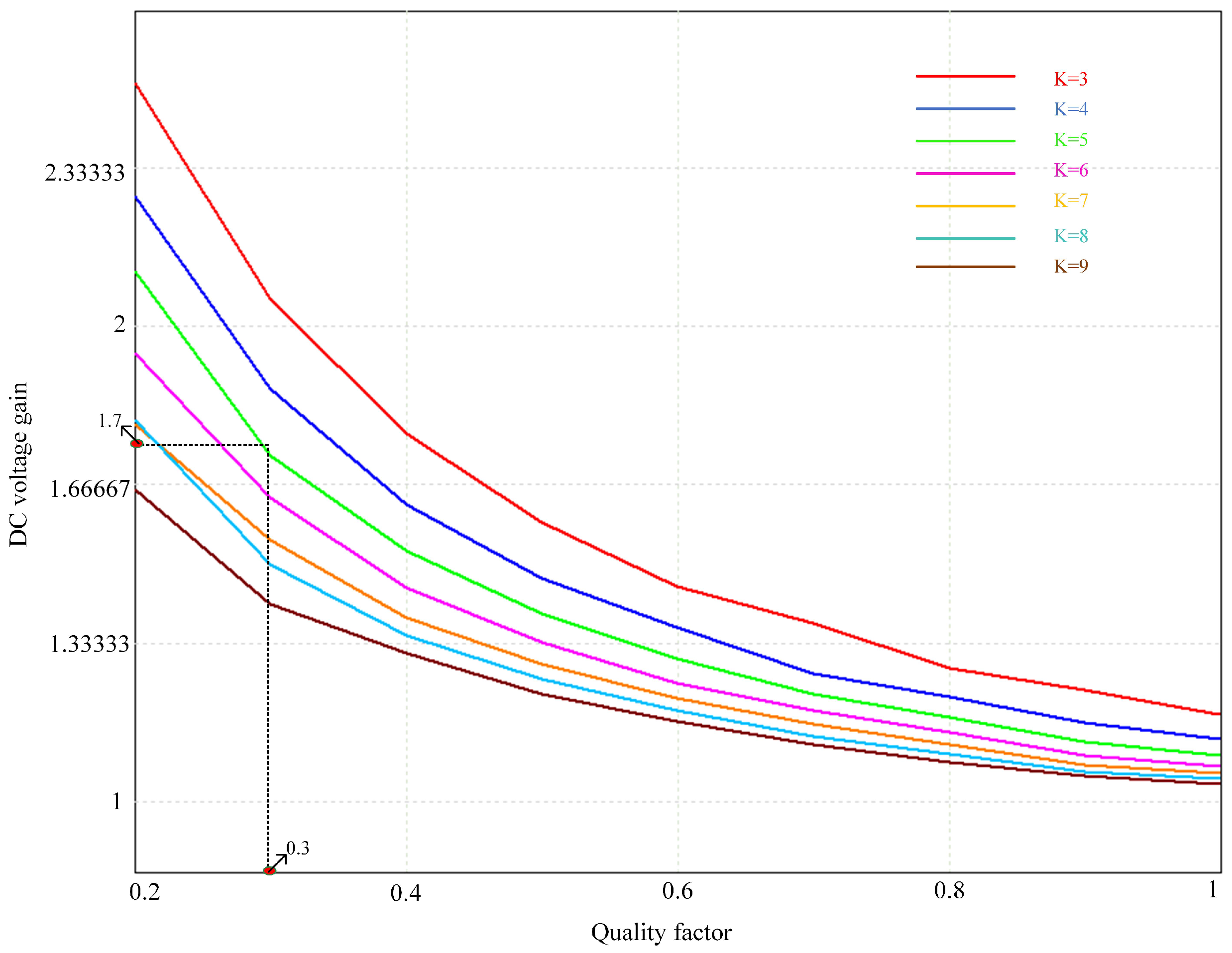
  • FDA-based design techniques are primarily reliant on engineering practice, such as how to choose the Q and K values, which is not universal, and the outcomes differ from one situation to the next;
  • Only the most basic soft switching and voltage gain needs are taken into account in the design.
An analytical approach combining the partial time-domain corrections and frequency domain is proposed in [9]. In this technique, the equivalent load in DCM is altered by using TDA. This method’s accurateness is considerably enhanced over FHA, but it still makes a large number of assumptions, which reduces its accuracy. For the LLC-RC, in [10], the authors developed an approach in which both the resonant factor and the equivalent load are adjusted, although the method of derivation is difficult and the accuracy increment is not apparent. The above-mentioned issues still remain despite efforts to increase accuracy through the methods of approaches based on FDA with partial and complete corrections in the time domain.
State space investigation is an additional option to be employed, which can describe the current and voltage waveforms accurately [24,25]. However, the interpretation and usage are convoluted and challenging. The literature available in [26,27] is based on operational modes and is mainly concentrated on analyzing the resonant voltage and current behavior according to different modes rather than calculating the DC gain. More valuable in directing the design is an exact DC gain characteristic rather than precisely stated current and voltage characteristics.
The LLC-RC has not been subjected to any additional assumptions in the TDA. There is a strong correlation between theoretical and actual results. The fundamental drawback of time-domain analysis is that it is difficult to solve nonlinear equations because of its complexity. Design techniques established on TDA have been developed to make maximum use of the LLC resonant tank. An automated computer-aided design technique based on the LLC converter power loss model is presented in [15], where the optimum design result may be reached by setting the parameters for the design variables to their limits. System voltage gain operating points are designed as the peak gain operating points of the LLC-RC in [8,14] depending on whether they are operating in PN or PON modes. The LLC resonant tank may be used to its full potential with this design technique; however, the ZVS operation for the primary switches may be compromised at the operating point of maximum gain. Additionally, the text fails to explicitly identify the optimization goal, which is mostly up to the designer. Because of the high processing requirements of these design methods, they are difficult to implement. It is necessary to solve all of the LLC-RC operation modes and boundary conditions in [15], which makes the design process more difficult. We need to find out about the PN and PON operating modes, as well as the boundary conditions that exist between them. Furthermore, because there is no set beginning point, there are a plethora of design options.
In this paper, a simplified analysis of the LLC resonant tanks’ DCMs has been thoroughly investigated in PO mode under the worst case instead of PN or PON modes. Due to the possibility of several resonant frequencies, DCM modeling for three or more resonant element converters based on FHA and prolonged descriptive function is highly approximate in nature. Numerous studies have attempted to solve analytical problems for multi-element resonant converters such as LLC, LCC, and LCLC using a state-space time domain method. Few authors have investigated the TDA operating above the resonant point of the LLC-RC. The majority of these publications make certain assumptions, such as a linear increasing magnetizing current, sinusoidal output current, and complete output diode conduction. The majority of these studies have focused solely on estimating the maximum voltage gain at or around the resonance point. In the current literature, there has not been much consideration devoted to the examination and derivation of closed-form solutions for ZVS angle, component stress, active power, RMS current, switch turn-off current, and other circuit design parameters in DCM mode. As a result, the circuit parameters are incorrectly selected.
This paper strives, by offering a precise model, to bridge this gap. LLC-RCs have demonstrated the exact derivation of the tank RMS current, tank capacitor voltage, converter voltage gain, peak stress, and ZVS. This research provides researchers with user-friendly technologies that allow them to quickly specify parameters, examine trade-offs, prototype the final product design quickly, and perform precise magnetic examination. As an action of the frequency, load, and other circuit parameters, closed-form solutions are developed for converter peak stress, tank capacitor voltage, voltage gain, ZVS angle, and tank RMS current. The rest of this article is structured in the following manner: the time-domain analysis introduction is presented in Section 2. Section 3 discusses the steady state time domain analysis. A complete step-by-step design procedure for LLC-RC is presented in Section 4. Then, the simulation and experimental results are presented in Section 5. Finally, the conclusions are provided in Section 6.

2. Time-Domain Analysis Introduction

The LLC-RC’s typical circuit is shown in Figure 1. During the first half of the switching cycle, there are three subintervals. As long as the voltage across the magnetizing inductor is held at (+ V o )/n, the subinterval is defined as “P”. The subinterval is “N” when the voltage is held down at ( V o )/n, and the “O” subinterval occurs when no current runs through the secondary side of the transformer [8]. The LLC-RC operates primarily in the following six modes of operation: PO, PON, PN, NP, NOP, and OPO, which are determined by the sequences of these three subintervals. An LLC-RC running in PO mode first operates in the P-subinterval, followed by the O-subinterval, for half of the switching time.
Figure 2 depicts the significant waveforms produced when the LLC-RC is working in the PO mode. The switch current i S 1 is negative before the driving signal S 1 is supplied; thus, its anti-parallel diode will turn on and perform the ZVS process on S 1 . In the same way, the remaining switches ( S 2 S 4 ) are capable of the ZVS process. The secondary diodes ( D 1 D 4 ) can accomplish ZCS functioning based on the waveform of the transformer secondary current i s e c . The PO and OPO modes of the LLC-RC are extremely efficient because the primary switches and secondary diodes operate in ZVS and ZCS modes, respectively [28]. Other operating modes, such as PON or PN modes, do not ensure ZVS functioning for the primary switches, resulting in worse overall system efficiency. The switching frequency in NOP or NP mode is higher than the resonance frequency, and the secondary diodes cannot perform ZCS. Design considerations include making sure it can function in OPO or PO modes across the complete working range. The other three analytical techniques had significant errors; therefore, the resonant tank components were designed using time-domain analysis. The analysis for PO mode is identical to that for the OPO mode, which follows in the next section.

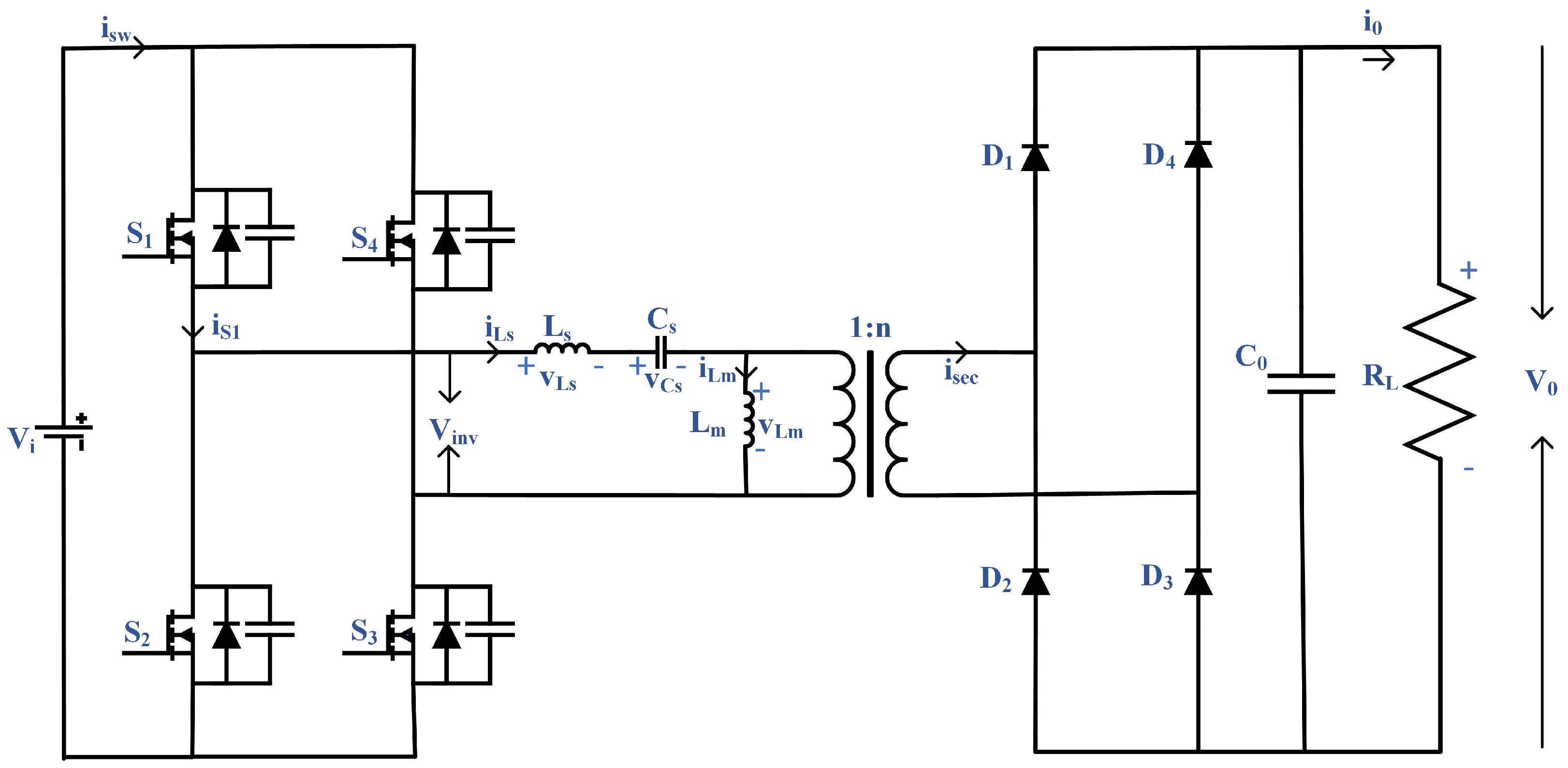
3. Steady State Time-Domain Analysis

The variable-frequency controlled LLC-RC’s steady state time-domain analysis is presented in this section. In order to keep the bridge stable, two complementary gating signals are used, each having a duty cycle of 0.5%. Figure 1 depicts the overall configuration of the LLC-RC in PO mode, as well as the corresponding equivalent circuit that results. Figure 3A,B illustrates the analogous circuits for an LLC resonant converter working in the P and O stages, respectively. In order to analyze the converter’s steady state performance, the following assumptions are made.
  • The rectifier diodes, MOSFET switches and transformer are ideal;
  • The filter capacitor is sufficiently big to maintain a stable voltage at the output;
  • The capacitance of a MOSFET is quite small;
  • The dead time between switches is not taken into account.
The reasons for choosing the PO operating mode are summarized as follows.
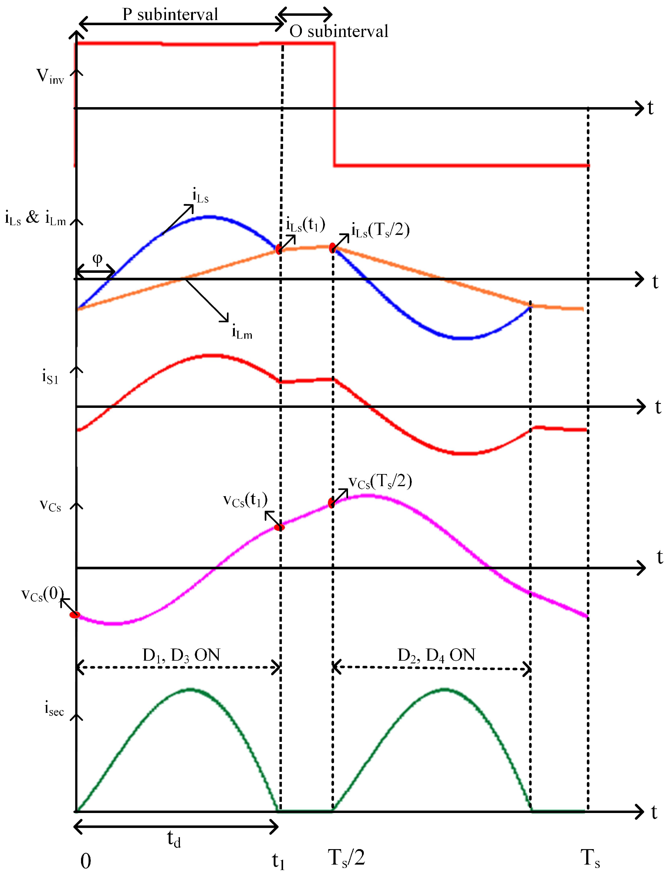
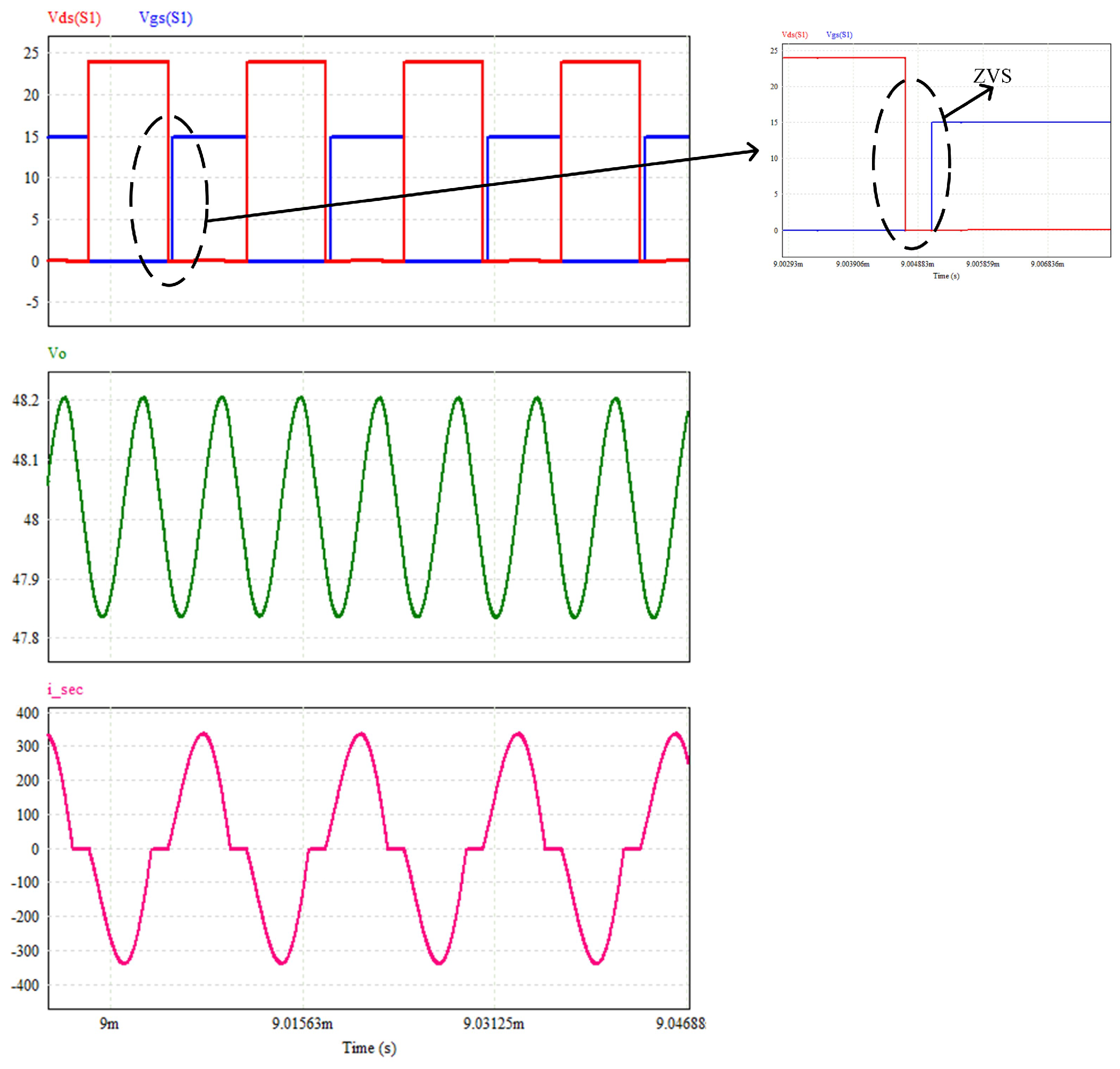
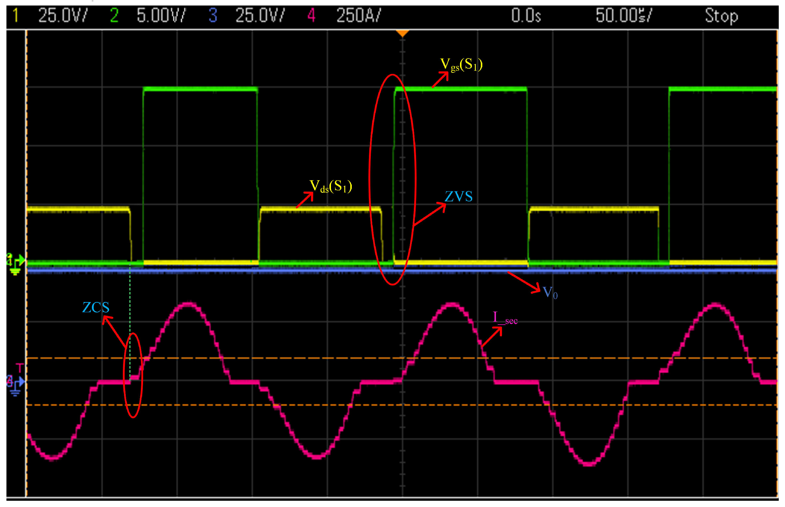
  • The most typical mode of operation for an LLC-RC is the PO mode. Generally, the LLC-RC is intended to operate in this mode in order to attain ZVS for the primary switches and ZCS for the secondary diodes;
  • The resonant tank control capabilities of an LLC converter can be increased by constructing it in the operation modes of PN or PON even when the peak gain operating point occurs in these modes [8,14]. The peak gain for the primary switch is also the barrier between ZVS and ZCS operation. When constructing an LLC-RC in PON or PN modes, the ZVS action may fail, reducing the efficiency of the converter;
  • Furthermore, to obtain the ZVS operation in the PON or PN operating mode, a large dead-time is required. Excessive dead-time will have a negative impact on the converter’s efficiency. As a result, in terms of soft switching, the PO mode is favored above the PN or PON modes;
  • In terms of performance, the PO mode is almost identical to the maximum gain mode. As a result, the voltage gain lost by using the worst-case PO operating mode design is negligible, and the PO mode may be utilized to estimate the peak gain as well;
  • For closed-loop designs, this guarantees control stability by using negative gain–frequency curve slopes in the PO mode. Because of this, the PO mode of operation is recommended for LLC converters. A control instability problem can arise when the operating point of the gain–frequency curve varies in PN or PON mode, which is when the gain–frequency curve is operated at its boundary.
Figure 2 depicts the LLC converter operational waveforms in boost mode. The resonant tank is driven by a square wave input generated by the full bridge’s variable switching frequency control. The ZVS angle is indicated by ϕ , which is a measurement of the exact ZVS and t d . Differential equations utilizing KCL/KVL have been developed for each mode. For the sake of analysis, the subsequent quantities have been defined:
Z 0 = L s C s
Z 1 = L s + L m C s
ω r = 1 L s C s
ω r 1 = 1 L s + L m C s
ω = ω s w ω r
K = L m L s
where Z 0 = characteristic impedance, L m = magnetizing inductance, L s = resonant inductance, C s = resonant capacitor, ω r = series resonant angular frequency, ω r 1 = parallel resonant angular frequency, ω = angular normalized frequency, and ω s w = angular switching frequency.

3.1. Energy Transfer Period (0 − T1)

The starting values of the magnetizing current, i L m , and resonant tank current, i L s , are identical. The currents have distinct wave patterns and deviate because the series resonant capacitor, C s , and inductor, L s , are in resonance, and the magnetizing inductor is restrained to the output voltage. The magnetizing current, i L m , increases linearly when the clamped output voltage (+ V o )/n is applied. i L s starts out with a negative value, crosses the zero line, and then equals i L m at time t 1 . According to KCL, the output rectifier is responsible for supplying any leftover current to the load. This period lasts until t 1 = t d T s w /2, where t d is the diode to switch conduction ratio. The differential equations that represent this mode are as follows:
V i V 0 n = L s d i L s ( t ) d t + v C s ( t )
i L s ( t ) = C s d v Cs ( t ) d t
i L m ( t ) = 1 L m 0 t V 0 n d t + i L m ( 0 )
Solving (7)–(9),
i L s ( t ) = i L s ( 0 ) cos ω r t + V i V 0 n v C s ( 0 ) Z 0 sin ω r t
i L m ( t ) = V 0 n L m t + i L m ( 0 )
v C s ( t ) = Z 0 i L s ( 0 ) sin ω r t + v C s ( 0 ) cos ω r t + V i V 0 n 1 cos ω r t
i 0 ( t ) = i L s ( t ) i L m ( t )

3.2. Freewheeling Period (t1 T s w /2)

The diodes are turned off naturally when i L m and i L s are equal at the completion of the first interval, and thus the secondary side no longer receives the primary side energy. Now, L m is not fixed to the output voltage; it begins to resonate with the series L s and C s , enabling the series resonant current to pass through it. Therefore, there is a shifting of resonant frequency from ω r to ω r 1 . This mode’s differential equations are as follows:
V i = L s d i L s ( t ) d t + v C s ( t ) + v L m ( t )
i L s ( t ) = C s d v C s ( t ) d t
v L m ( t ) = L m d i L m ( t ) d t
Solving the above equations, we get
i L s ( t ) = i L s t 1 cos ω r 1 t t 1 v C s t 1 Z 1 sin ω r 1 t t 1 + V i Z 1 sin ω r 1 t t 1
v C s ( t ) = Z 1 i L s t 1 sin ω r 1 t t 1 + v C s t 1 cos ω r 1 t t 1 + V i 1 cos ω r 1 t t 1
i L s ( t ) = i L m ( t )
The transfer of energy only occurs between 0 and t 1 , where t 1 alters on t d . As a result, t d cannot be considered as a fixed value when computing the starting current, or the voltage values and the voltage gain, for LLC-RC since it changes depending on the load circumstances. Closed-form expressions would not apply to all loading scenarios. Therefore, for an exact TDA, starting values of capacitor voltage, resonant current, and voltage gain are proven to be implicit functions of t d and ω . Thus, the average output current may be expressed as follows:
I 0 = 2 T s w 0 t 1 i L s ( t ) i L m ( t ) d t
I 0 = 2 T s w ω r i L s ( 0 ) sin ω r t 1 + V i v 0 n v c s ( 0 ) z 0 1 cos ω r t 1 V 0 ω r 2 n ω r L m t 1 2 2 i L m ( 0 ) ω r t 1
The steady-state waveforms exhibit anti-half-wave symmetry. Therefore, the evaluation may be conducted for half a switching cycle using the resulting circumstances:
i L s ( 0 ) = i L m ( 0 ) = i L s T s W 2
v C s ( 0 ) = v C s T s W 2
i L s t 1 = i L m t 1
Equations to evaluate the resonant capacitor voltage, v C s (0), initial series resonant current, i L s (0), and voltage gain are obtained by a reduction of the resultant set of equations. As a consequence, the resultant equations can be written in the following form:
i L s ( 0 ) = V i α 1 + n G V i β 1
v C s ( 0 ) = V i α 2 + n G V i β 2
where
α 1 = 2 Z 1 sin ( x ) cos ( y ) + Z 0 cos ( x ) sin ( y ) L
β 1 = Z 1 sin ( x ) cos ( y ) + Z 0 cos ( x ) sin ( y ) + Z 1 sin ( x ) Z 0 sin ( y ) L
α 2 = sin ( x ) sin ( y ) Z 1 2 Z 0 2 L
β 2 = Z 1 2 sin ( x ) sin ( y ) Z 1 Z 0 ( 1 cos ( x ) cos ( y ) ) L
L = 2 Z 1 Z 0 + 2 Z 1 Z 0 cos ( x ) cos ( y ) sin ( x ) sin ( y ) Z 1 2 + Z 0 2
x = ω r ω s w t d π
y = ω r 1 ω s w 1 t d π
Therefore, for the DCM boost operating mode, the voltage gain, G, is expressed as follows:
G = V 0 n V i = sin ( x ) + α 1 Z 0 ( 1 cos ( x ) ) + α 2 sin ( x ) t d T s w Z 0 2 L m + sin ( x ) + β 2 sin ( x ) + β 1 Z 0 ( 1 cos ( x ) )
The negative current of i L s (0) is the turn-off current because of the anti-half wave symmetry of the steady state waveforms, as illustrated in (22). To simplify the equation, we may replace (32) and (33) in (21) to obtain the following value of the average output current:
I 0 = A 1 ( sin ( x ) ) + B 1 ( 1 cos ( x ) ) n G V i x 2 2 ω r L m i C s ( 0 ) x ω π
where
A 1 = i L s ( 0 )
B 1 = V i n G V i v C s ( 0 ) Z 0
The equivalent AC load can be calculated by using the above expression of average output voltage:
V o = I o R l o a d
R l o a d = V 0 A 1 sin ( x ) + B 1 ( 1 cos ( x ) ) G V i x 2 2 ω r L m i C s ( 0 ) x ω π
In DCM, R l o a d is reliant on t d and ω , which is given in the expression (39). In contrast to the usual equation given by R a c = 8 π 2 R e q , this is applicable for the continuous conduction mode of operation, i.e., in the above resonance operation. The equation used to determine the ZVS angle is
ϕ = π ω tan 1 A 1 B 1
The resonant tank inductor current’s RMS value is given by
i L s R M S = π ω I R M S P + I R M S O L S + L m L S
where
I R M S P = A 1 2 + B 1 2 x 2 1 4 sin 2 x + tan 1 A 1 B 1 + sin 2 tan 1 A 1 B 1
I R M S O = A 2 2 + B 2 2 y 2 1 4 sin 2 y + tan 1 A 2 B 2 + sin 2 tan 1 A 2 B 2
I R M S P and I R M S O are the RMS currents for the modes P and O, respectively. Mode O variables are defined as follows:
A 2 = i L s t 1
B 2 = V i v C s t 1 Z 1

4. Complete Step-by-Step Design of an LLC-RC

In this section, the design of an LLC-RC is explained in detail. The following are the primary design steps:
  • Determine the ratio of transformer turns;
  • Determine the amount of DC gain required;
  • Select Q and K in such a way that the output voltage gain matches the desired G m a x when the converter is working in PO mode;
  • Determine the resonant components.
Table 1 summarizes the system requirements for a typical LLC-RC application.
Step 1: Determine the ratio of transformer turns
The maximum and minimum DC gain requirements for the resonant LLC tank may be derived using the transformer turns ratio.
The n s p (secondary to primary transformer turns ratio) should be calculated as follows:
n s p = V 0 m a x + V 0 m i n 2 V i n n o m = 1.7143
A well-balanced resonant LLC converter’s functioning at low circulating current and at frequencies below and above the resonance is ensured by this method of calculating n s p . In addition, the resonant tank’s buck and boost areas are both covered by unity gain at the resonant frequency.
Step 2: Determine the amount of DC gain required
The required minimum and maximum values of DC gain are calculated as shown below:
G d c m i n = V 0 m i n V i n m a x n s p = 0.874
G d c m a x = V 0 m a x V i n m i n n s p = 1.666
The DC gain range of 0.87 to 1.7 is chosen for overloading and other realistic parasitics.
Step 3: Select Q and K
From the gain vs quality factor curves and normalized frequency vs gain curves as shown in Figure 4 and Figure 5, Q and K are selected as 0.3 and 5, respectively.
Step 4: Determine the resonant components
L S = Q R 0 r a t e d p r i 2 π f r = 0.0468   μ H
C s = 1 2 π f r Q R 0 r a t e d p r i = 54.134   μ F
L m = K L s = 0.23396   μ H
where
R 0 r a t e d p r i = R 0 r a t e d n s p
Table 2 shows the different values of minimum and maximum gains, normalized frequencies, switching frequencies, resonant frequency, RMS, and peak currents of switch, average, and peak currents of the diode, as well as stress on the capacitor at different set of K values with the same quality factor. From the table below, it is observed that values of Q = 0.3 and K = 5 contribute to a narrow range of frequency deviation, low turn-off current, and low circulating currents compared to other conditions. Low-voltage stress on the resonant capacitance and higher power density owing to the smaller size of resonant capacitance and overall magnetics are also ensured by this combination of components.

Loss Examination of LLC-RC

By turning on the primary power MOSFETs with ZVS and turning off the secondary rectifier diodes with ZCS, the LLC-RC reduces the overall switching loss. The losses for MOSFET are conduction, turn-off, and driving losses. The losses for the diode are conduction losses. Core and copper losses are transformer losses. Table 3 summarizes the different component losses and their associated calculations [29,30].

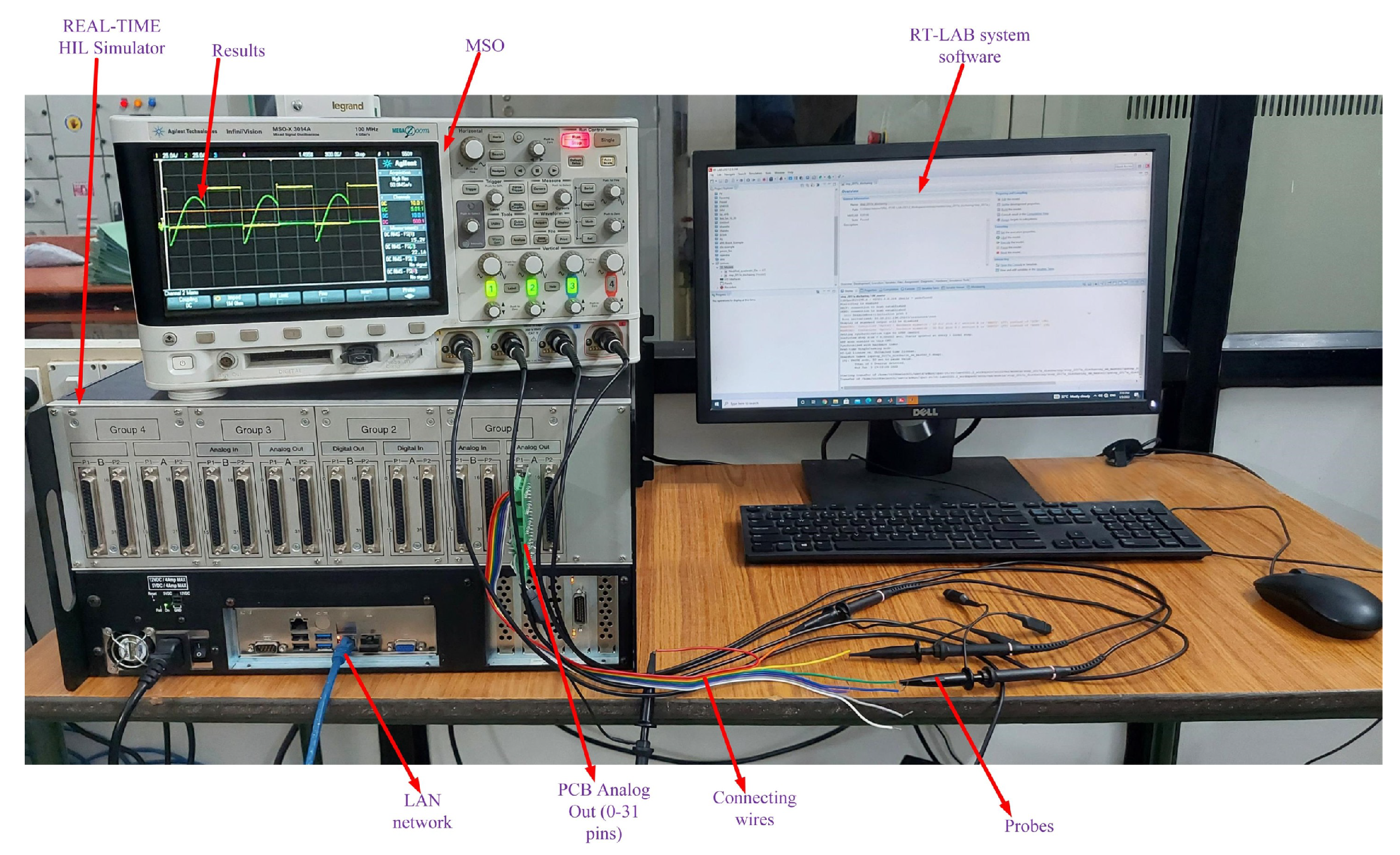
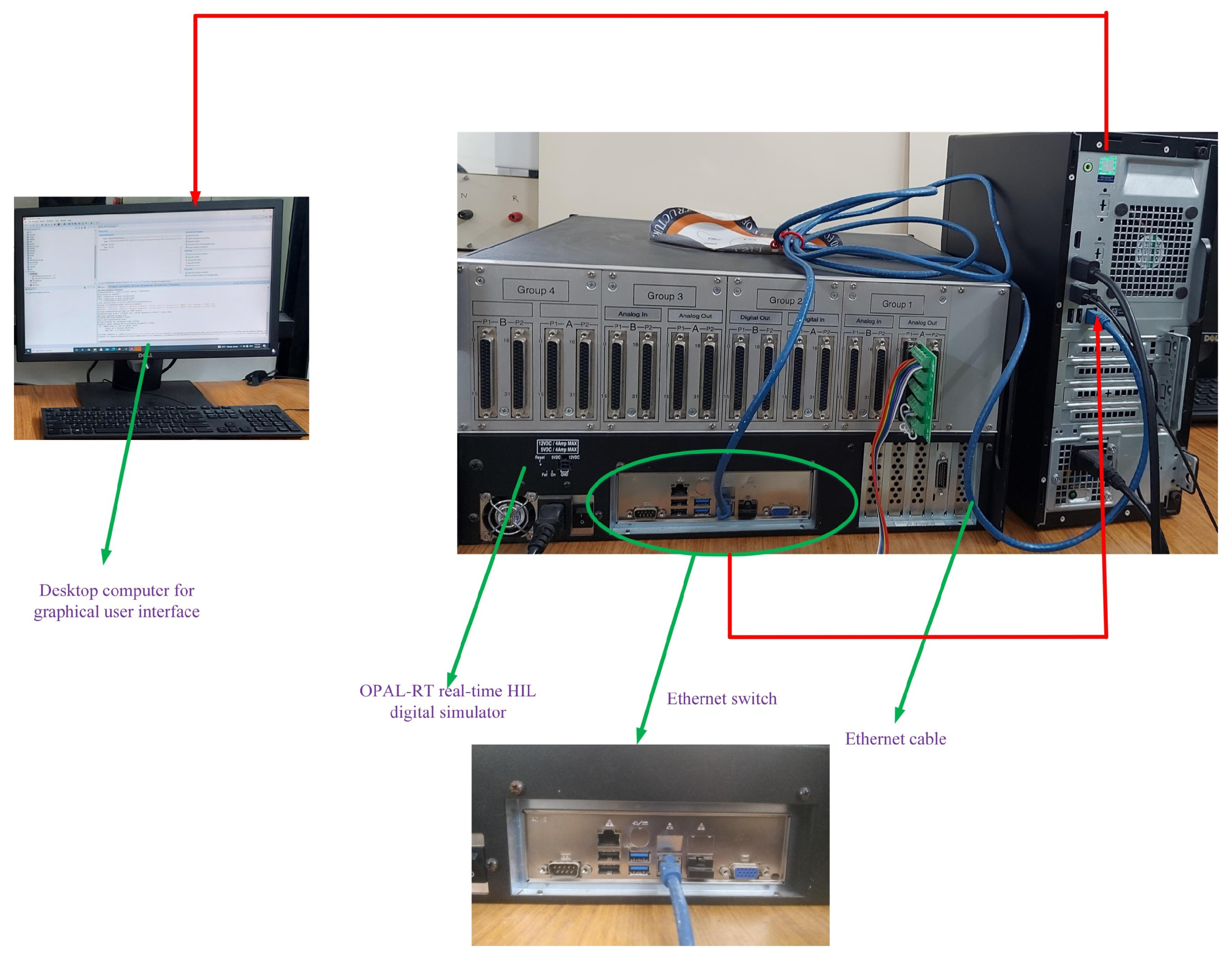
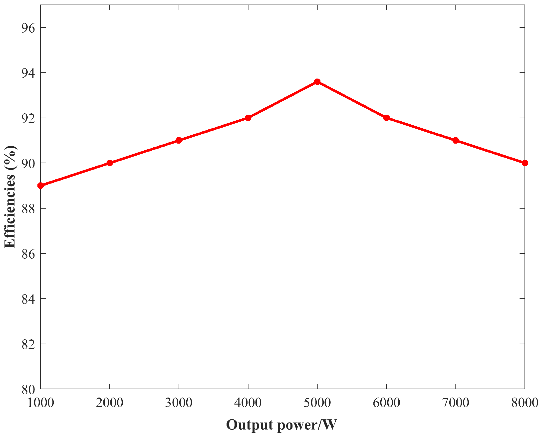
5. Simulation and Experimental Results

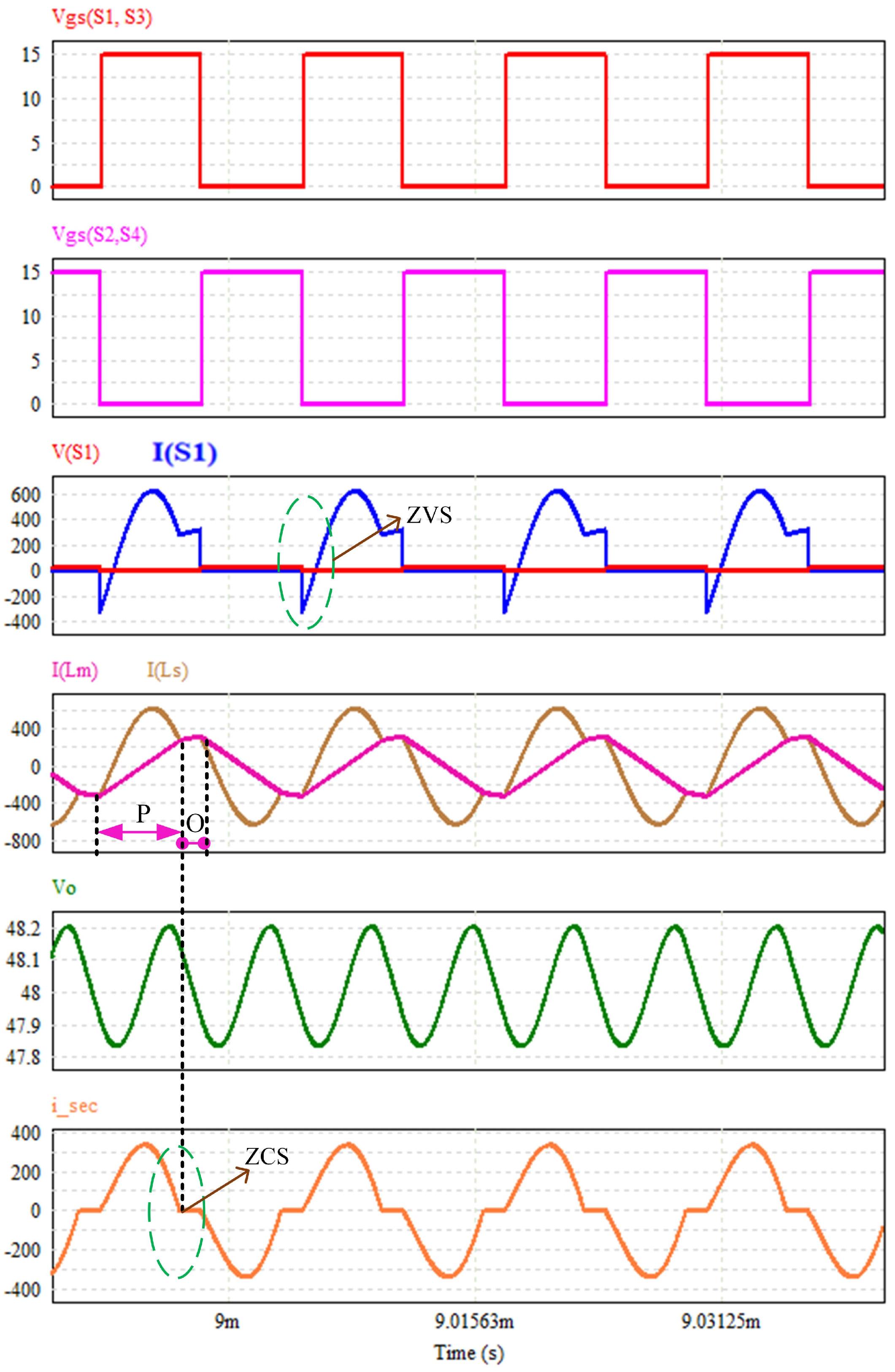
5.1. Simulation Results

Figure 6 shows the simulation results for the LLC-RC at minimum input voltage with the optimum design values. V S 1 and i S 1 indicate that the voltage across the switch and current through the switch at rated power when the input voltage equals 24 V. i s e c is the secondary current flowing through the rectifier diodes. With the optimum designed values, the output voltage V 0 of the converter is regulated at 48 V. It is clearly observed that the converter is functioning in PO mode. The currents i L m and i L s share the same starting currents at the beginning of the stage P. After that, they separate in various wave shapes. As L m is confined to + V o /n, i L m expands linearly, whereas i L s changes sinusoidally, since L s and C s are in resonance. Both the secondary rectifier diodes are switched off when i L m and i L s intersects at the end of stage P, and then the LLC-RC advances to stage O. In addition to that, i S 1 lags behind V S 1 , which indicates that the input impedance is inductive and the ZVS operation for primary switches is achieved. Furthermore, i s e c drops to zero well before the relevant rectifier turn-off signal arrives, ensuring that the rectifier diodes does not suffer from reverse recovery issues and is able to operate in ZCS mode.
Figure 7 shows the simulation waveforms of the gate driver signal ( V g s ) and drain-source voltage ( V d s ) of the switch S 1 . The worst situation for the ZVS operation of the converter is when the input voltage hits the minimum value and the output power reaches the maximum value. It is observed that the V d s is completely zero before the V g s is turned on. Therefore, for the whole operating range, ZVS operation is achieved.

5.2. Experimental Results

The proposed model of LLC-RC is verified using HIL simulator OP5700, RT-LAB, programmable control board (PCB-E06-0560), MSOx3014T, and probes. The PCB is used to communicate between both the simulation and real controller using analog outputs and digital inputs. The configuration of the real-time implementation setup is depicted in Figure 8. HIL systems are frequently utilized for real-time simulations of engineering systems before implementing the prototyping tests. Stacks are capable of rapidly creating and synchronizing prototypes. The plant and controller are placed in OPAL-RT to enable the system to operate at real-time clock speeds. This process can be considered as a real-time system simulation due to high-speed nanosecond to microsecond OPAL-RT sampling rate. The user’s PC is used to execute the RT-digital LAB’s simulator commands. RT-LAB is used to edit, build, load, and execute the prototype. The requirements and specifications of the HIL stack are given in Table 4. The circuit parameters pertaining to various components are shown in Table 5.
Figure 9 shows the implementation method of HIL testing. It consists of an OPAL-RT real-time HIL simulator, ethernet switch, ethernet cable, and desktop computer for the graphical user interface (GUI). The RT-LAB software for OPAL-RT is used in HIL testing. The ethernet cable is connected between the ethernet switch of OPAL-RT and desktop computer for the GUI.
Figure 10 shows the experimental results of the LLC-RC at the worst operating point; i.e., at minimum input voltage with rated power. From the results, it is observed that the converter is operating in PO mode with a switching frequency of 77 KHz—a small deviation from theoretical 78 KHz because of parasitics of the converter. In addition, i S 1 lags behind the V S 1 in the entire operating range, which indicates that the input impedance is inductive and the ZVS action for primary switches is realized. The secondary current i s e c operates in discontinuous conduction mode; therefore, the secondary rectifier diodes achieve ZCS operation.
To verify the primary switches’ ZVS functionality, an experimental waveform of the V g s and V d s of switch S 1 is shown in Figure 11. It is observed that the V d s is completely zero before the V g s is turned on. Therefore, for the whole operating range, ZVS operation is achieved.
Figure 12 shows the efficiency curve of the LLC-RC at minimum input voltage with various output power levels. At the output power of 5000 W, the measured maximum efficiency is about 93.4%, and at rated power, a measured maximum efficiency of 90.1% is achieved.
Table 6 shows the comparison of simulation and experimental values of the designed converter. Due to the internal parasitics of the converter, there is a slight variation from simulation to experiment.

6. Conclusions

This article proposed a complete step-by-step precise TDA for LLC-RC working in DCM boost mode with secondary current. The converter operates in PO mode throughout its working range, and for primary MOSFET switches, it guarantees the ZVS and ZCS for the secondary rectifier. The generated closed-form analytical formulas for ZVS angle, voltage gain, and RMS current are applicable at any operating point, below or above the resonant frequency. The worst-case scenario is taken into account while designing the converter, including the converter operating mode, ZVS for primary switches, RMS current of the resonant inductor, and voltage stress for the resonant capacitor. Then, all the potential design candidates are listed in Table 2, with different values of K that provide a narrow frequency variation, low turn-off current, and lower circulating currents. Measured maximum efficiencies of 93.4% and 90.1% are achieved at the output power of 5000 W and at the rated output power, respectively. Table 6 shows the comparison of simulation and experimental values of the designed converter. Finally, both the simulation and experimental results were provided in order to validate the theoretical analysis.

Author Contributions

Conceptualization, K.K.G. and E.D.; Data curation, K.K.G.; Formal analysis, K.K.G.; Investigation, K.K.G. and E.D.; Methodology, K.K.G. and E.D.; Software, K.K.G. and E.D.; Supervision, E.D.; Validation, E.D.; Visualization, E.D.; Writing—original draft, K.K.G. and E.D.; Writing—review & editing, E.D. All authors have read and agreed to the published version of the manuscript.

Funding

This research received no external funding.

Institutional Review Board Statement

Not applicable.

Informed Consent Statement

Not applicable.

Data Availability Statement

Not applicable.

Conflicts of Interest

The authors declare no conflict of interest.The funders had no role in the design of the study; in the collection, analyses, or interpretation of data; in the writing of the manuscript, or in the decision to publish the results.

References

  1. Zhou, Q.; Liu, Y.; Li, Z.; He, Z. A Coupled-Inductor Interleaved LLC Resonant Converter for Wide Operation Range. Energies 2022, 15, 315. [Google Scholar] [CrossRef]
  2. Manuel, D.; Kutschak, M.; Pulsinelli, F.; Rodriguez, N.; Morales, D.P. On the Practical Evaluation of the Switching Loss in the Secondary Side Rectifiers of LLC Converters. Energies 2021, 14, 5915. [Google Scholar]
  3. Tran, Y.K.; Freijedo, F.D.; Dujic, D. Open-loop power sharing characteristic of a three-port resonant LLC converter. CPSS Trans. Power Electron. Appl. 2019, 4, 171–179. [Google Scholar] [CrossRef]
  4. Wei, Y.; Altin, N.; Luo, Q.; Nasiri, A. A high efficiency, decoupled on-board battery charger with magnetic control. In Proceedings of the 2018 7th International Conference on Renewable Energy Research and Applications (ICRERA), Paris, France, 14–17 October 2018; pp. 920–925. [Google Scholar]
  5. Wei, Y.; Luo, Q.; Alonso, J.M.; Mantooth, A. A magnetically controlled single-stage AC–DC converter. IEEE Trans. Power Electron. 2020, 35, 8872–8877. [Google Scholar] [CrossRef]
  6. Yang, B.; Chen, R.; Lee, F.C. Integrated magnetic for LLC resonant converter. In Proceedings of the APEC. Seventeenth Annual IEEE Applied Power Electronics Conference and Exposition (Cat. No. 02CH37335), Dallas, TX, USA, 10–14 March 2002; pp. 346–351. [Google Scholar]
  7. Wei, Y.; Wang, Z.; Luo, Q.; Mantooth, H.A. MATLAB GUI Based Steady State Open-Loop and Closed-Loop Simulation Tools for Different LLC Converters With all Operation Modes. IEEE Open J. Ind. Appl. 2021, 2, 320–336. [Google Scholar] [CrossRef]
  8. Fang, X.; Hu, H.; Shen, Z.J.; Batarseh, I. Operation mode analysis and peak gain approximation of the LLC resonant converter. IEEE Trans. Power Electron. 2011, 27, 1985–1995. [Google Scholar] [CrossRef]
  9. Ivensky, G.; Bronshtein, S.; Abramovitz, A. Approximate analysis of resonant LLC DC-DC converter. IEEE Trans. Power Electron. 2011, 26, 3274–3284. [Google Scholar] [CrossRef]
  10. Liu, J.; Zhang, J.; Zheng, T.Q.; Yang, J. A modified gain model and the corresponding design method for an LLC resonant converter. IEEE Trans. Power Electron. 2016, 32, 6716–6727. [Google Scholar] [CrossRef]
  11. Deng, J.; Li, S.; Hu, S.; Mi, C.C.; Ma, R. Design methodology of LLC resonant converters for electric vehicle battery chargers. IEEE Trans. Veh. Technol. 2013, 63, 1581–1592. [Google Scholar] [CrossRef]
  12. Deng, J.; Mi, C.C.; Ma, R.; Li, S. Design of LLC resonant converters based on operation-mode analysis for level two PHEV battery chargers. IEEE/ASME Trans. Mechatron. 2014, 20, 1595–1606. [Google Scholar] [CrossRef]
  13. Hu, Z.; Wang, L.; Qiu, Y.; Liu, Y.F.; Sen, P.C. An accurate design algorithm for LLC resonant converters—Part I. IEEE Trans. Power Electron. 2015, 31, 5435–5447. [Google Scholar] [CrossRef]
  14. Hu, Z.; Wang, L.; Qiu, Y.; Liu, Y.F.; Sen, P.C. An accurate design algorithm for LLC resonant converters—Part II. IEEE Trans. Power Electron. 2015, 31, 5448–5460. [Google Scholar] [CrossRef]
  15. Yu, R.; Ho, G.K.Y.; Pong, B.M.H.; Ling, B.W.K.; Lam, J. Computer-aided design and optimization of high-efficiency LLC series resonant converter. IEEE Trans. Power Electron. 2011, 27, 3243–3256. [Google Scholar] [CrossRef] [Green Version]
  16. Xu, H.; Yin, Z.; Zhao, Y.; Huang, Y. Accurate design of high-efficiency LLC resonant converter with wide output voltage. IEEE Acess 2017, 5, 26653–26665. [Google Scholar] [CrossRef]
  17. Bhat, A.S. Analysis and design of LCL-type series resonant converter. IEEE Trans. Ind. Electron. 1994, 41, 118–124. [Google Scholar] [CrossRef]
  18. Steigerwald, R.L. A comparison of half-bridge resonant converter topologies. IEEE Trans. Power Electron. 1988, 3, 174–182. [Google Scholar] [CrossRef]
  19. Bhat, A.S. A generalized steady-state analysis of resonant converters using two-port model and Fourier-series approach. IEEE Trans. Power Electron. 1998, 13, 142–151. [Google Scholar] [CrossRef]
  20. Forsyth, A.J.; Ward, G.A.; Mollov, S.V. Extended fundamental frequency analysis of the LCC resonant converter. IEEE Trans. Power Electron. 2003, 18, 1286–1292. [Google Scholar] [CrossRef]
  21. Lee, B.H.; Kim, M.Y.; Kim, C.E.; Park, K.B.; Moon, G.W. Analysis of LLC resonant converter considering effects of parasitic components. In Proceedings of the INTELEC 2009-31st International Telecommunications Energy Conference, Incheon, Korea, 18–22 October 2009; pp. 1–6. [Google Scholar]
  22. Lin, R.L.; Lin, C.W. Design criteria for resonant tank of LLC DC-DC resonant converter. In Proceedings of the IECON 2010-36th Annual Conference on IEEE Industrial Electronics Society Conference, Glendale, CA, USA, 7–10 November 2010; pp. 427–432. [Google Scholar]
  23. Jung, J.H.; Kwon, J.G. Theoretical analysis and optimal design of LLC resonant converter. In Proceedings of the 2007 European Conference on Power Electronics and Applications, Aalborg, Denmark, 2–5 September 2007; pp. 1–10. [Google Scholar]
  24. Batarseh, I.; Liu, R.; Ortiz-Conde, A.; Yacoub, A.; Siri, K. Steady state analysis and performance characteristics of the LLC-type parallel resonant converter. In Proceedings of the 1994 Power Electronics Specialist Conference-PESC’94, Taipei, Taiwan, 20–25 June 1994; pp. 597–606. [Google Scholar]
  25. Vukšić, M.; Beroxsx, S.M.; Mihoković, L. The multiresonant converter steady-state analysis based on dominant resonant process. IEEE Trans. Power Electron. 2010, 26, 1452–1468. [Google Scholar] [CrossRef]
  26. Lazar, J.F.; Martinelli, R. Steady-state analysis of the LLC series resonant converter. In Proceedings of the APEC 2001 Sixteenth Annual IEEE Applied Power Electronics Conference and Exposition (Cat. No. 01CH37181), Anaheim, CA, USA, 4–8 March 2001; pp. 728–735. [Google Scholar]
  27. Oeder, C.; Bucher, A.; Stahl, J.; Duerbaum, T. A comparison of different design methods for the multiresonant LLC converter with capacitive output filter. In Proceedings of the 2010 IEEE 12th Workshop on Control and Modeling for Power Electronics (COMPEL), Boulder, CO, USA, 28–30 June 2010; pp. 1–7. [Google Scholar]
  28. Costa, V.S.; Perdigao, M.S.; Mendes, A.S.; Alonso, J.M. Evaluation of a variable-inductor-controlled LLC resonant converter for battery charging applications. In Proceedings of the IECON 2016-42nd Annual Conference of the IEEE Industrial Electronics Society, Piazza Adua, Firenze, Italy, 24–27 October 2016; pp. 5633–5638. [Google Scholar]
  29. Fang, Z.; Cai, T.; Duan, S.; Chen, C. Optimal design methodology for LLC resonant converter in battery charging applications based on time-weighted average efficiency. IEEE Trans. Power Electron. 2014, 30, 5469–5483. [Google Scholar] [CrossRef]
  30. Yang, C.H.; Liang, T.J.; Chen, K.H.; Li, J.S.; Lee, J.S. Loss analysis of half-bridge LLC resonant converter. In Proceedings of the 2013 1st International Future Energy Electronics Conference (IFEEC), Tainan, Taiwan, 3–6 November 2013; pp. 155–160. [Google Scholar]
Figure 1. Full-bridge LLC resonant converter.
Energies 15 03634 g001
Figure 2. LLC converter steady state waveforms in PO mode.
Energies 15 03634 g002
Figure 3. Equivalent circuits in PO mode, (A) energy transfer period in P mode, (B) freewheeling period in O mode.
Energies 15 03634 g003
Figure 4. Plots of quality factor and DC voltage gain with different values of K.
Energies 15 03634 g004
Figure 5. Plots of normalized switching frequency and DC voltage gain with different values of Q.
Energies 15 03634 g005
Figure 6. Simulations waveforms at minimum input voltage.
Energies 15 03634 g006
Figure 7. Simulation waveforms of the gate driver signal ( V g s ) and drain-source voltage ( V d s ).
Energies 15 03634 g007
Figure 8. HIL experimental setup for the LLC-RC.
Energies 15 03634 g008
Figure 9. The HIL testing setup.
Energies 15 03634 g009
Figure 10. Experimental waveforms of V S 1 and I S 1 , V 0 and I s e c at minimum input voltage with rated power.
Energies 15 03634 g010
Figure 11. Experimental waveforms of the V g s and V d s showing ZVS operation under the worst condition.
Energies 15 03634 g011
Figure 12. Efficiency of the converter at various output powers.
Energies 15 03634 g012
Table 1. System Specifications.
ParameterDesignatorValue
Input voltage range V i n _ m i n V i n _ m a x 24–32 V
Input nominal voltage V i n _ n o m 28 V
Output voltage V 0 _ m i n V i n _ m a x 48 V
Rated output power P o 8000 W
Series resonant frequency f r 100 kHz
Table 2. Design candidates.
QK G dcmin - G dcmax Normalized Frequency f sw (KHz) f r (KHz) i sw _ RMS (A) i sw _ peak (A) v sw _ peak (V) i d _ average (A) i d _ peak (A) i Lm _ peak (A) i Cs _ RMS (A) v Cs _ peak (V) L s (µH)C s (µF) L m (µH)
0.330.871.18118100170.83499.753262.83206.80318.64341.6611.800.046854.1340.14
0.331.670.8585100254.83718.983283.96323.76541.90509.6655.860.046854.1340.14
0.340.871.23123100151.110438.4603262.75198.84228.96302.2209.9750.046854.1340.187
0.341.670.8181100224.47653.423283.94330.063411.17448.9551.030.046854.1340.187
0.350.871.27127100141.24406.283262.71194.390177.290282.499.0150.046854.1340.234
0.351.660.7878100208.490626.143283.39336.37329.79416.9822.380.046854.1340.234
0.360.871.3130100135.69387.153262.73191.74144.39271.398.460.046854.1340.281
0.361.670.7474100204.63636.743283.94354.88276.15409.2745.4800.046854.1340.281
0.370.871.33133100131.89374.223262.62189.66120.75263.788.0430.046854.1340.328
0.371.670.7171100202.39648.973283.89368.91236.090404.7843.630.046854.1340.328
0.380.871.35135100129.52365.463262.64188.450104.12259.0497.790.046854.1340.374
0.381.660.6969100199.90655.563283.34376.83205.27399.8042.100.046854.1340.374
0.390.871.37137100127.68358.873262.58187.4291.11255.377.570.046854.1340.421
0.391.670.6666100202.79683.983283.62395.59181.28405.5840.850.046854.1340.421
0.3100.871.38138100126.58354.13262.68186.9281.53253.167.470.046854.1340.468
0.3101.660.6464100203.75701.413283.38407.05161.79407.5039.770.046854.1340.468
Table 3. Loss analysis for LLC-RC.
Name of the DeviceLoss Calculation
MOSFETGate-Driving loss = 4 1 2 C g s V g s 2 f s
Turn-off loss = 4 f s v i i i t r + t f 2
Conduction loss in MOSFET = loss in MOSFET+ loss in
antiparallel diode = 4 i error 2 R d s + 4 V d i error + i error 2 R b o d y
TransformerCore loss = 2 K h f s m B a c n M c o r e
Copper loss = 2 i error 2 R error + i error 2 R error
DiodeConduction loss of diodes = 4 1 2 P 0 V 0 V F + i error 2 R d
Table 4. Hardware-in-loop (HIL) system specifications.
Name of the DeviceOP5700 Simulator
FPGAXilinx® Virtex® 7 FPGA on VC707 board
Processing speed: 200 ns–20 μ s
I/O Lines256 lines, routed to eight analog or digital,
16 or 32 channels
High-speed communication ports16SFP sockets, up to 5 GBps
I/O connectorsFour panels of four DB37 connectors
Monitoring connectorsFour panels of RJ45 connectors
PC interfaceStandard PC connectors
Power ratingInput: 100–240 VAC, 50–60 Hz, 10/5 A, Power: 600 W
Table 5. Parameters pertaining to various circuit components.
Name of the ComponentParameter
Primary MOSFET ( S 1 S 4 )VISHAY SQJQ140E
Rectifier diodes ( D 1 D 4 )VISHAY VS-403CNQ100PbF
Turns ratio ( n s p )1:1.72
Resonant capacitor ( C s )54.134 µF
Resonant inductor ( L s )0.04679 µH
Magnetizing inductor ( L m )0.23395 µH
Table 6. Comparison of simulation and experiment parameters.
Design ParameterSimulation ValueExperimental Value
Q0.30.3
K55
f s w (KHz)7877
f r (KHz)10098.61
i s w _ R M S (A)208.49206.2
i s w _ p e a k (A)626.14619.3
V s w _ p e a k (V)3224
i d _ a v e r a g e (A)83.3980.5
i d _ p e a k (A)336.37331
i L m _ p e a k (A)329.79325.1
i C s _ R M S (A)416.98409.5
v C s _ p e a k (V)22.3822
L s (µH)0.04680.0468
C s (µF)54.13454.134
L m (µH)0.233960.23396
Publisher’s Note: MDPI stays neutral with regard to jurisdictional claims in published maps and institutional affiliations.

