Abstract
This paper proposes a step-up DC–DC converter for a power electronic circuit for standalone photovoltaic systems with battery energy storages. The proposed DC–DC converter effectively converts low DC battery voltage into high DC-link voltage. It operates with soft-switching characteristics, which can reduce switching power losses. The proposed converter operates without output voltage feedback, which simplifies its control design. The operation principle of the proposed converter was described, along with the overall system configuration. The experimental results were discussed for the 500-W prototype system using a 12-V lead-acid battery.
1. Introduction
The standalone photovoltaic (PV) systems are widely used in the off-grid areas. In general, the standalone PV systems consist of photovoltaic panels, a maximum power point tracking (MPPT) charger, a battery energy storage, and a standalone inverter [1,2]. As shown in Figure 1, The MPPT charger extracts the maximum power from the PV panels and charges the battery. The battery stores excess power, which can be stably supplied to loads. A 12-V lead-acid battery is widely used since the lead-acid battery is relatively inexpensive and easy to handle. The standalone inverter has the intermediate DC–DC converter and the single-phase inverter. This inverter converts the low battery voltage into the sinusoidal AC output voltage.
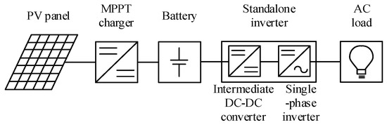
Figure 1.
Configuration of the Standalone PV Systems.
In a typical standalone inverter, the full-bridge inverter is used with a bulky line-frequency transformer. However, the line-frequency transformer increases the cost and the size and lowers the overall power efficiency. In order to cope with these drawbacks, various types of DC–DC converters utilizing high-frequency transformers have been designed for the intermediate DC–DC converter [3,4]. These converters provide high power conversion efficiency along with the advantages of small size and light weight.
The current-fed DC–DC converters are suitable for the intermediate DC–DC converter, which has low input voltage and high current batteries. It has the advantages such as a low input current ripple, low conduction loss, high voltage conversion ratio, and reduced transformer turns’ ratio [5,6,7,8]. However, the current-fed converters have a boost inductor at the input terminal, which results in large size and high cost. In addition, they have high voltage spikes for power switches resulting from the stored energy at the boost inductor. On the other hand, the voltage-fed DC–DC converters have low primary switch voltage stress, minimal components, and small size [9,10,11,12,13,14,15,16,17,18,19,20,21]. The voltage-fed converters can be classified into the unidirectional core excitation topology and the bidirectional core excitation topology. The unidirectional core excitation topology such as flyback and forward converters has low magnetic core utilization since the magnetic flux is unbalanced and saturated [9]. Therefore, the unidirectional core excitation topology converters are used at low power level applications. Compared to the unidirectional core excitation converters, the bidirectional core excitation topology such as push–pull, half-bridge, and full-bridge converters have higher magnetic core utilization [10,11,12,13]. Therefore, the bidirectional core excitation topology converters are used for higher power level applications.
As a voltage-fed converter, the push–pull converter has desirable features for an intermediate DC–DC converter [13,14]. The push–pull converter has two power switches with a common ground, which can have simple gate-driving circuits. Additionally, it has a simple structure, galvanic isolation, and high voltage conversion ratio. If the soft switching is achieved, it has low switching losses, high efficiency, and improved electromagnetic interference.
Unfortunately, the major drawback of the push–pull converter is that the voltage stress of the switches is twice the input voltage. To reduce the switching losses, several topologies are proposed. The active clamp or auxiliary circuits are employed to absorb voltage spike and achieve soft switching [14,15]. However, it increases the components, control complexity, size, and cost of the designed converter. The resonant techniques are employed to suppress voltage spike [16,17,18,19,20,21,22], which provides the soft switching operation of power switches at the primary side. However, the switching power losses should be considered at the secondary side, where power diodes generate switching power losses during their switching operations.
This paper proposes a step-up DC–DC converter, which can effectively convert low battery voltage into high dc-link voltage for the standalone PV systems. As shown in Figure 2, the proposed step-up DC–DC converter consists of the push–pull converter and resonant voltage doubler rectifier. The resonant voltage doubler rectifiers provide a higher voltage conversion ratio and reduce the high turns’ ratio in the transformer [16,17,18,19,20,21,22]. It operates in the discontinuous conduction mode (DCM) to reduce the switching losses and to remove the reverse-recovery losses for the power diodes at the secondary side. The primary switches operate under the zero-voltage switching (ZVS) operation. The diodes are turned off at zero current due to resonance between leakage inductance Llk and resonant capacitors Cr1 and Cr2. The proposed step-up DC–DC converter can operate with the open loop condition by removing the auxiliary circuits for the output voltage feedback control. To show the entire control strategy for the proposed step-up DC–DC converter, the overall PV standalone system was suggested. The 500-W prototype was implemented with minimal components. This paper is organized as follows. In Section 2, the step-up DC–DC converter is analyzed. Its operation principle (2.1) is described for the steady-state operation condition. Its design guidelines (2.2) are also presented for the high-frequency transformer and the resonant circuit components. In Section 3, the control strategy of the DC–DC converter is presented. The overall system configuration (3.1) is described. The detailed control schemes (3.2) for power electronic circuits are introduced. In Section 4, the experimental results are discussed for the 500-W prototype system. Twelve-V lead-acid batteries were utilized for battery energy storages. A step-down DC–DC converter converted the photovoltaic power into the battery power. Experimental results verified the effectiveness of the proposed DC–DC converter. Finally, Section 5 gives the concluding remarks.
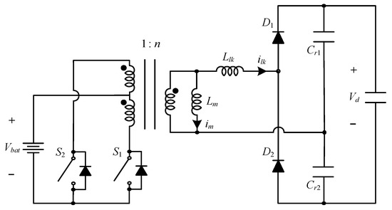
Figure 2.
Proposed step-up DC–DC converter.
2. Proposed Converter
2.1. Operation Principle
The proposed step-up converter, as shown in Figure 2, consisted of the push–pull converter and the resonant voltage doubler rectifier. The switches S1 and S2 operated alternately with 50% duty of the switching cycle. The resonant voltage doubler rectifier was composed of the diodes D1 and D2 and resonant capacitors Cr1 and Cr2. It was driven in the DCM to reduce current stress of the switches and achieve zero current turn off the diodes. The following assumptions were made for simplified analysis.
- The switches S1 and S2 were ideal except for their body diodes DS1 and DS2, respectively.
- The high frequency transformer had a turn ratio 1:n and was modeled as the magnetizing inductances Lm and leakage inductance Llk.
- The output voltage of DC link Vd was constant because the DC link capacitor Cd was sufficiently large.
- The resonant capacitors Cr1 and Cr2 had the equal capacity to operate symmetrically.
The proposed high step-up DC–DC converter was divided into six operation modes. Figure 3 and Figure 4 show the three operation modes and their theoretical waveforms, respectively. Prior to Mode 1, the switch S2 was turned on, allowing the current to flow slightly. The current ilk across the leakage inductance Llk was zero.
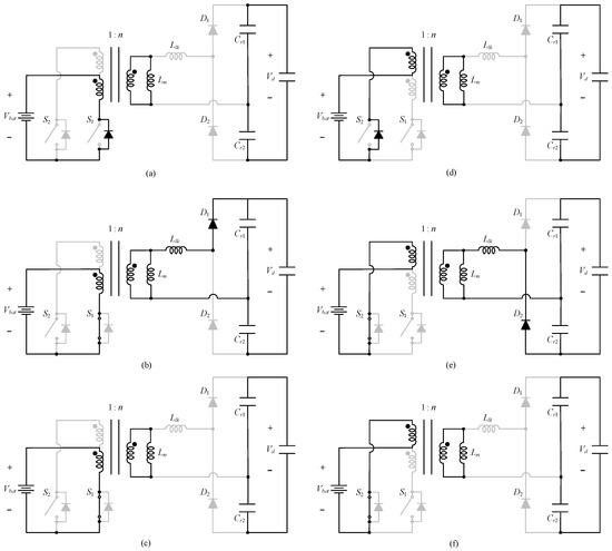
Figure 3.
Operation modes: (a) Mode 1; (b) Mode 2; (c) Mode 3; (d) Mode 4; (e) Mode 5; and (f) Mode 6.
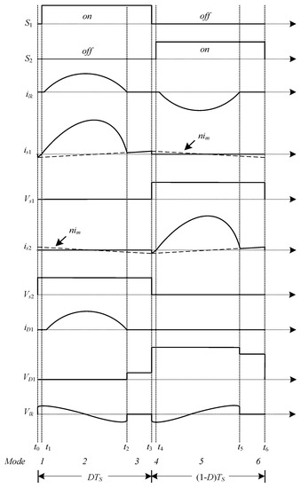
Figure 4.
Waveforms of the proposed DC–DC converter according to operating modes of DCM.
Mode 1 [t0, t1]: At t0, the switch S2 was turned off with the current stress reduced. The voltage across switch S2 was rapidly charged to twice the battery voltage Vbat. The drain-source current iS1 across switch S1 discharged the drain-source voltage VS1 across switch S1 to zero and flowed through the body diode DS1. The magnetizing current im increased linearly as follows:
Mode 2 [t1, t2]: At t1, the switch S1 was turned on at zero voltage. The power was transferred to the DC link through the transformer. The inductance Llk and resonant capacitors Cr1 and Cr2 resonated and the current ilk flowed through the diode D1. The state equation can be written as follows:
where the resonant capacitor Cr is as:
From Equations (2)–(4), the voltage vcr1 across the resonant capacitor Cr1 is derived as:
Since the initial value of ilk is zero, ilk is obtained as:
where Ilk,peak is the peak of ilk. The impedance Zr and the angular resonance frequency ωr are written as follows:
The voltage across the leakage inductance Llk is obtained as:
In the primary side, the voltage of each transformer had Vbat. Thus, the voltage across the switch S2 was twice Vbat and the im still increased linearly. The total iS1 current is as:
Mode 3 [t2, t3]: At t2, the current ilk became zero. Thus, the diode D1 was turned off at zero current and the reverse recovery losses were removed. Then, voltage across leakage inductance Llk was zero and the voltage across diode D1 became the reverse voltage of the leakage inductance as follows:
The current im continues to increase linearly as follows:
If magnetizing inductance was sufficiently large, the magnetizing current im was almost zero and the switch S1 could be turned off at zero current.
The analysis of Modes 4, 5, and 6 is omitted since it is symmetrically repeated during the remaining half switching cycle.
2.2. Design Guidelines
To eliminate the reverse recovery losses of the diode and reduce current stress of the switches, the current ilk decreased to zero before t3. From Equation (7), ilk is expressed as follows:
where Δt is the resonant period as follows:
Since the proposed converter operated in the DCM condition, the resonant period was shorter than the half of TS. Therefore, the switching frequency fs should be lower than the resonant frequency fr as follows:
From Equation (15), the resonant capacitors Cr1 and Cr2 can be designed as:
In order to reduce the size and the cost of the converter, a high frequency transformer was used in the proposed converter. Figure 5 shows the winding structure of the proposed transformer. The transformer was separately coiled around the primary and secondary windings utilizing a double E core. This method can be used to integrate a resonant inductor and the transformer. The leakage inductance of the transformer constituted the resonant inductor. It was possible to remove the passive component and resonant inductor. Based on the proposed method, the high frequency transformer of the converter was designed.
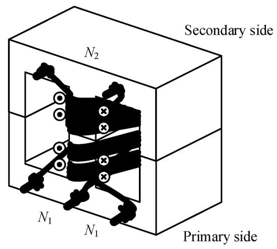
Figure 5.
The winding structure for the large leakage inductance.
3. Control Strategy
3.1. Overall System
Figure 6 shows the overall system diagram of the PV standalone converter with the simple controller, which included the entire control. It was realized in low power applications. As shown in Figure 6, the overall system consisted of the synchronous buck converter, the proposed DC–DC converter, and the conventional full-bridge inverter. The synchronous buck converter extracted the power from the panels through the conventional perturb and observe (P&O) MPPT control and charged the battery. The proposed DC–DC converter boosted the low battery voltage to the sufficient voltage to the inverter operation. The conventional full-bridge inverter converted the DC voltage into the sinusoidal AC output voltage.
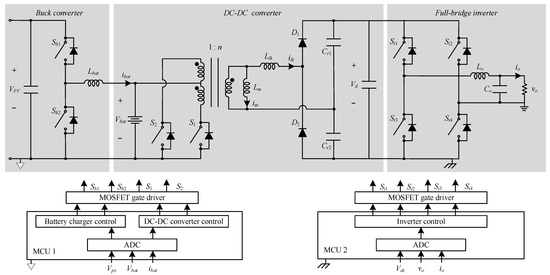
Figure 6.
Overall system diagram of the PV standalone converter with the simple controller.
3.2. Control Scheme
To design the control system for the overall standalone PV system with the open loop operation, two independent microcontrollers were used for the primary side and the secondary side. The primary side microcontroller controlled the buck converter and the proposed DC–DC converter. The buck converter performed the conventional P&O MPPT algorithm to extract the maximum power from PV arrays. The proposed DC–DC converter operated with 50% duty of the switching cycle in open loop control. This operation scheme effectively provided the sufficient voltage for the inverter operating without sensing the DC voltage. It had a fast dynamic response and a simple control structure with low-cost implementation. The secondary side microcontroller controlled the conventional full-bridge inverter for its standalone operation. Figure 7 shows the control diagram for the full-bridge inverter. The proposed control design reduced the control complexity and simplified its associated circuit layouts by eliminating the auxiliary circuits for the output voltage feedback control.
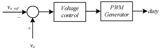
Figure 7.
Control diagram for the full-bridge inverter.
4. Experimental Results
To verify the theoretical analysis of the proposed converter for the steady-state condition, the proposed converter was simulated using PSIM 2020a. The major components and parameters are shown in Table 1. Figure 8 shows simulation waveforms in the half load. Figure 8a shows the current and voltage waveforms of the switch S1 according to the on/off switching states of switches in the one switching cycle. It shows that the current across switch flowed negatively before the on state of the power switch. Thus, the switches were turned on at the zero voltage. Additionally, it shows that the current across switches was reduced by the resonance of the leakage inductance and resonant capacitors before the switch was turned off. Thus, the current stresses across the switches were minimized when the switches were turned off. Figure 8b shows current and voltage waveforms of the diode in the one switching cycle. It shows that the current across the diode decreased to zero. Then, the voltage across leakage inductance became zero and the voltage across the diode became the reverse voltage of the leakage inductance. Thus, the diodes were turned off at the zero current, and the reverse recovery losses were removed.

Table 1.
Major components and parameters.
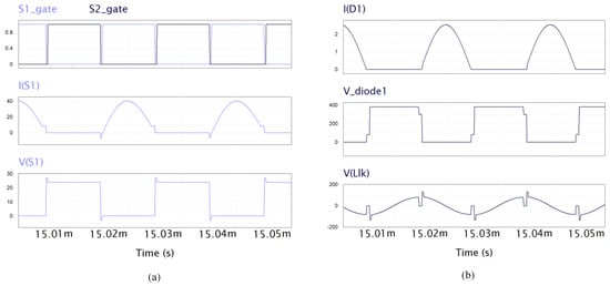
Figure 8.
The simulation waveforms: (a) current and voltage waveforms of the switch; (b) current and voltage waveforms of the diode.
To validate the performance of the proposed converter, a 500-W prototype was developed. Figure 9 shows the picture for the experimental step up of the prototype converter. Figure 10 shows the experimental waveforms of the proposed prototype converter. Figure 10a shows the measured current and voltage waveforms of the switch. The switches were turned off with soft switching at zero voltage and turned on at the minimized current. Figure 10b shows the measured current and voltage waveforms of the diode. Before the diode D1 was reversely biased, the diode current iD1 reached zero and achieved the zero-current turn-off of the diode. After the diode current reached zero, there were parasitic voltage oscillations due to the resonance between stray inductance and capacitance. Figure 11 shows the output current io and the output voltage vo where vo and io are sinusoidal with 60 Hz. Figure 12 shows the power efficiency of the proposed converter at half-load condition according to the battery voltage. The efficiency was 93.1% at battery voltage 12 V.
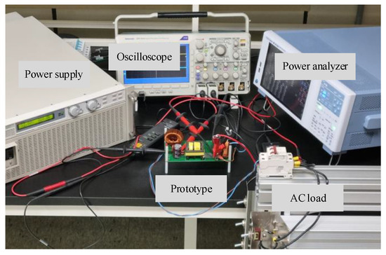
Figure 9.
The experimental setup of a 500-W prototype converter.
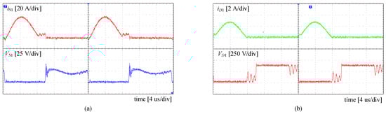
Figure 10.
Experimental waveforms: (a) current and voltage waveforms of the switch; (b) current and voltage waveforms of the diode.
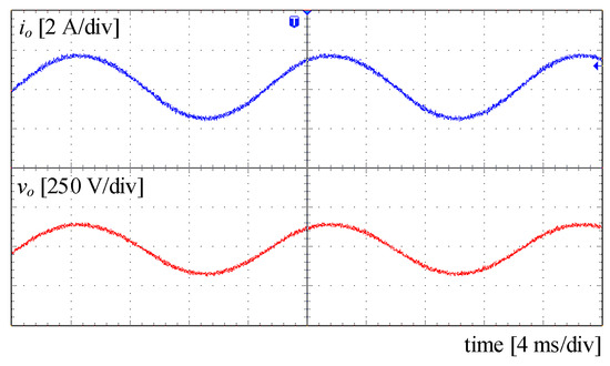
Figure 11.
Experimental waveforms: current and voltage waveforms of the output.
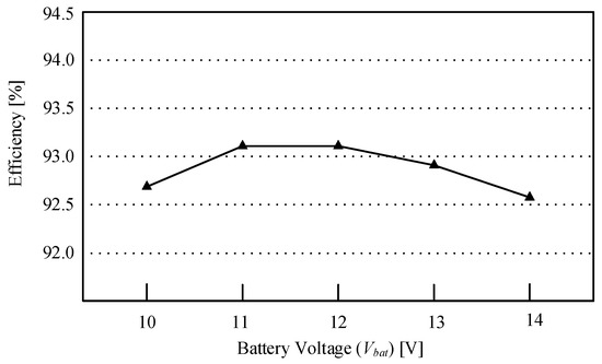
Figure 12.
The overall efficiency at half load depending on the charged battery voltage.
5. Concluding Remarks
This paper proposed a step-up DC–DC converter for a power electronic circuit for standalone photovoltaic systems with battery energy storages. The proposed converter operates with soft-switching characteristics in the DCM. The primary switches achieved zero voltage turn on without active clamp circuit or auxiliary circuit to suppress the voltage spike. The secondary diodes achieved zero current turn off. Additionally, the resonant voltage doubler rectifier provided high voltage conversion capability and reduced the high turns’ ratio in the transformer with current stress reduction when the primary switches were turned on. Thus, the efficiency increased at minimal components. The control without output voltage control was suggested by using two independent controllers, which simplifies its control design. The overall system configuration and its operation principle were described. The 500-W prototype was experimented at input battery voltage range from 10 to 14 V. It had 93.1% maximum efficiency using 12-V lead-acid batteries.
Author Contributions
Y.-G.O. performed the experiments, analyzed the data, and mainly wrote the manuscript; W.-Y.C. analyzed the experimental data and edited the manuscript; J.-M.K. managed the project and edited the manuscript. All authors have read and agreed to the published version of the manuscript.
Funding
This research was supported by the research fund of Hanbat National University in 2021.
Institutional Review Board Statement
Not applicable.
Informed Consent Statement
Not applicable.
Data Availability Statement
Not applicable.
Conflicts of Interest
The authors declare no potential conflict of interest.
References
- Pazikadin, A.R.; Rifai, D.; Ali, K.; Mamat, N.H.; Khamsah, N. Design and Implementation of Fuzzy Compensation Scheme for Temperature and Solar Irradiance Wireless Sensor Network (WSN) on Solar Photovoltaic (PV) System. Sensors 2020, 20, 6744. [Google Scholar] [CrossRef] [PubMed]
- Wang, W.; Ruan, X. A Modified Reference of an Intermediate Bus Capacitor Voltage-Based Second-Harmonic Current Reduction Method for a Standalone Photovoltaic Power System. IEEE Trans. Power Electron. 2016, 31, 5562–5573. [Google Scholar] [CrossRef]
- Abbasi, M.; Lam, J. A Step-Up Transformerless, ZV-ZCS High-Gain DC/DC Converter with Output Voltage Regulation Using Modular Step-Up Resonant Cells for DC Grid in Wind Systems. IEEE J. Emerg. Sel. Top. Power Electron. 2017, 5, 1102–1121. [Google Scholar] [CrossRef]
- Abbasi, M.; Lam, J. A Very High-Gain-Modular Three-Phase AC/DC Soft-Switched Converter Featuring High-Gain ZCS Output Rectifier Modules without Using Step-Up Transformers for a DC Grid in Wind Systems. IEEE Trans. Ind. Appl. 2018, 54, 3723–3736. [Google Scholar] [CrossRef]
- Kwon, J.M.; Kim, E.H.; Kwon, B.H.; Nam, K.H. High-Efficiency Fuel Cell Power Conditioning System with Input Current Ripple Reduction. IEEE Trans. Ind. Electron. 2009, 56, 826–834. [Google Scholar] [CrossRef]
- Wu, Q.; Wang, Q.; Xu, J.; Li, H.; Xiao, L. A High-Efficiency Step-Up Current-Fed Push-Pull Quasi-Resonant Converter with Fewer Components for Fuel Cell Application. IEEE Trans. Ind. Electron. 2017, 64, 6639–6648. [Google Scholar] [CrossRef]
- Piegari, L.; Rizzo, R.; Spina, I.; Tricoli, P. Optimized Adaptive Perturb and Observe Maximum Power Point Tracking Control for Photovoltaic Generation. Energies 2015, 8, 3418–3436. [Google Scholar] [CrossRef]
- Barros, L.A.M.; Tanta, M.; Sousa, T.J.C.; Afonso, J.L.; Pinto, J.G. New Multifunctional Isolated Microinverter with Integrated Energy Storage System for PV Applications. Energies 2020, 13, 4016. [Google Scholar] [CrossRef]
- Kwon, J.M.; Kwon, B.H.; Nam, K.H. High-efficiency module-integrated photovoltaic power conditioning system. IET Power Electron. 2009, 2, 410–420. [Google Scholar] [CrossRef]
- Tran, Y.K.; Freijedo, F.D.; Dujic, D. Open-loop power sharing characteristic of a three-port resonant LLC converter. CPSS Trans. Power Electron. Appl. 2019, 4, 171–179. [Google Scholar] [CrossRef]
- Li, H.; Jiang, Z. On Automatic Resonant Frequency Tracking in LLC Series Resonant Converter Based on Zero-Current Duration Time of Secondary Diode. IEEE Trans. Power Electron. 2016, 31, 4956–4962. [Google Scholar] [CrossRef]
- Ma, X.; Wang, P.; Bi, H.; Wang, Z. A Bidirectional LLCL Resonant DC-DC Converter with Reduced Resonant Tank Currents and Reduced Voltage Stress of the Resonant Capacitor. IEEE Access 2020, 8, 125549–125564. [Google Scholar] [CrossRef]
- Huynh, D.M.; Ito, Y.; Aso, S.; Kato, K.; Teraoka, K. New Concept of the DC-DC Converter Circuit Applied for the Small Capacity Uninterruptible Power Supply. In Proceedings of the 2018 International Power Electronics Conference (IPEC-Niigata 2018-ECCE Asia), Niigata, Japan, 20–24 May 2018; pp. 3086–3091. [Google Scholar]
- Wu, Q.; Wang, Q.; Xu, J.; Xiao, L. A Wide Load Range ZVS Push-Pull DC/DC Converter with Active Clamped. IEEE Trans. Power Electron. 2017, 32, 2865–2875. [Google Scholar] [CrossRef]
- Wu, T.F.; Hung, J.C.; Tsai, J.T.; Tsai, C.T.; Chen, Y.M. An Active-Clamp Push-Pull Converter for Battery Sourcing Applications. IEEE Trans. Ind. Appl. 2008, 44, 196–204. [Google Scholar] [CrossRef]
- Tarzamni, H.; Babaei, E.; Esmaeelnia, F.P.; Dehghanian, P.; Tohidi, S.; Sharifian, M.B.B. Analysis and Reliability Evaluation of a High Step-Up Soft Switching Push–Pull DC–DC Converter. IEEE Trans. Reliab. 2020, 69, 1376–1386. [Google Scholar] [CrossRef]
- Wang, Y.; Liu, Q.; Ma, J.; Chen, L.; Ma, H. A New ZVCS Resonant Voltage-fed Push-pull Converter for Vehicle Inverter Application. In Proceedings of the 2013 IEEE International Symposium on Industrial Electronics, Taipei, Taiwan, 28–31 May 2013. [Google Scholar]
- Ekkaravarodome, C.; Bilsalam, A.; Tantiviwattanawongsa, P.; Thounthong, P. High Step-Up DC-DC Push-Pull Resonant Based on low Cost half-wave Class-D Rectifier. In Proceedings of the 2019 Research, Invention, and Innovation Congress (RI2C), Bangkok, Thailand, 11–13 December 2019. [Google Scholar]
- Ekkaravarodome, C.; Bilsalam, A.; Tantiviwattanawongsa, P.; Thounthong, P. DC-DC High Conversion Ratio Push-Pull Resonant Converter Based on Voltage Double Rectifier. In Proceedings of the 2019 Research, Invention, and Innovation Congress (RI2C), Bangkok, Thailand, 11–13 December 2019. [Google Scholar]
- Thippayanet, R.; Ekkaravarodome, C.; Jirasereeamornkul, K.; Chamnongthai, K.; Kazimierczuk, M.K.; Higuchi, K. Push-pull zero-voltage switching resonant DC-DC converter based on half bridge class-DE rectifier. In Proceedings of the 2013 IEEE 10th International Conference on Power Electronics and Drive Systems (PEDS), Kitakyushu, Japan, 22–25 April 2013; pp. 1162–1167. [Google Scholar]
- Ekkaravarodome, C.; Sukanna, S.; Bilsalam, A.; Nilphong, S.; Jirasereeamongkul, K.; Higuchi, K. Design of a Balanced Push-Pull Resonant Converter with a Voltage Doubler Class-DE Rectifier. In Proceedings of the 2019 Research, Invention, and Innovation Congress (RI2C), Bangkok, Thailand, 11–13 December 2019. [Google Scholar]
- Jia, P.; Mei, Y. Derivation and Analysis of a Secondary-Side LLC Resonant Converter for the High Step-Up Applications. IEEE J. Emerg. Sel. Top. Power Electron. 2021, 9, 5865–5882. [Google Scholar] [CrossRef]
Publisher’s Note: MDPI stays neutral with regard to jurisdictional claims in published maps and institutional affiliations. |
© 2021 by the authors. Licensee MDPI, Basel, Switzerland. This article is an open access article distributed under the terms and conditions of the Creative Commons Attribution (CC BY) license (https://creativecommons.org/licenses/by/4.0/).