Abstract
Copper sinter paste has been recently established as a robust die-attach material for high -power electronic packaging. This paper proposes and studies the implementation of copper sinter paste materials to create top-side interconnects, which can substitute wire bonds in power packages. Here, copper sinter paste was exploited as a fully printed interconnect and, additionally, as a copper clip-attach. The electrical and thermal performances of the copper-sinter paste interconnections (“sinterconnects”) were compared to a system with wire bonds. The results indicate comparable characteristics of the sinterconnect structures to the wire-bonded ones. Moreover, the performance of copper sinterconnects in a power module was further quantified at higher load currents via finite element analysis. It was identified that the full-area thermal and electrical contact facilitated by the planar sinterconnects can reduce ohmic losses and enhance the thermal management of the power packages.
1. Introduction
Power electronic device packaging, a critical bridge between semiconductor devices and their applications, has become a bottleneck for applications of high-power silicon and wide-bandgap (WBG) devices. Many recent studies have been performed to revolutionize power packaging materials and related processing, i.e., top-side interconnects and bottom-side, die-attach materials, insulators, encapsulants, and thermal interface materials [1,2].
Considering top (or front)-side interconnects, thick aluminum (Al) wire bond is the most widely used technology, but wire bonds often represent the weakest part of power modules. The current loading ability of Al wires cannot meet a higher current density per wire [3,4]. Since the maximum electrical current is limited to 10 A per 500 µm–diameter Al wire, for high-power applications, multiple wire bonds are needed [5]. This has, in turn, sacrificed reliability and increased manufacturing costs. Wire bonding technology furthermore inhibits double-sided cooling and 3D integration [6]. Finally, wire bond interconnects located between semiconductor pads and the package capacitively and/or inductively couple circuit nodes. This results in diminishing electrical isolation, increasing crosstalk, increased noise and, in general, reduced performance, especially under high current and high-frequency operation [7,8,9,10,11].
Several approaches have been proposed to substitute thick, Al wire bonds. Among recent proposals, solutions based on Copper (Cu) materials have gained a great deal of attention. Cu has several advantages over Al, such as a greater reliability at elevated temperatures, higher mechanical stability, superior electrical and thermal conductivity as well as compatibility with Cu-metallization of die-pads which alleviates the Al-Cu intermetallic growth concerns. A variety of Cu-based interconnects has been recently reported, i.e., Cu-clips, Cu-ribbons, Cu-pins, thin-film Cu, as well as thick Cu layers [12,13,14]. Additionally, two planar, top-side technologies, using metal-coated flexible foils, called Skin [15] and SiPLIT [11], were proposed and investigated by corporations Siemens and Semikron, respectively. In SiPLIT, an entire structure is covered by a soft, epoxy, insulation film applied by a vacuum-based lamination process. This is followed by the application of a laser ablation process to expose contacts. A Cu layer is then deposited by sputtering a seed layer and then electroplating. In the final step, the seed layer is removed by wet chemical etching. Similarly, in Skin process, a pre-structured polyimide film, coated with silver (Ag) paste, is used as a top-side interconnect substrate [15]. Nonetheless, SiPLIT and Skin processes are classified as complex because they require several different types of machinery.
On the other hand, Cu sinter pastes have been recently implemented merely as reliable bottom-side (or die-attach) materials for high-temperature and high-power power applications [16,17,18,19]. Indeed, it has been verified that Cu particles can be sintered in reducing atmospheres, such as hydrogen or gaseous formic acid, at low temperatures, since these reduction atmospheres reduce the Cu oxides to Cu [20]. By exploiting the advantages of drop-on-demand jet printing, this paper demonstrates how planar, top-side interconnects were directly fabricated by using a related Cu-sinter paste and process.
In conventional clip-bonding technology, a solid Cu bridge is soldered to the die surface. However, using solder materials amplifies reliability issues and limits the working temperature of the devices down to 200 °C at maximum. The brittleness of intermetallic compounds and low creep-resistance, as well as inferior thermal fatigue properties due to different thermal expansions of copper and solder materials, are some of the intrinsic issues with solders [21,22,23,24]. In this work a modified Cu clip-attach interconnect, in which Cu sinter paste was utilized, instead of solder paste, for attaching Cu clips to a direct-bond-copper- (DBC) substrate, is studied, in addition to fabrication and analysis of a fully printed version.
2. Materials and Methods
2.1. Fabrication of Top-Side Interconnects
For the fabrication of top-side interconnects, multi-chip, insulated-gate bipolar transistor (IGBT) power module sub-assemblies were used as test-vehicles. The IGBT and diode dies with a thickness of 300 µm were already soldered to DBC substrates. The dies had a Cu finish to facilitate Cu bonding. The top-side interconnect structures were fabricated in three distinct structures, shown in Figure 1. The following subsections summarize the subsequent fabrication and processing operations, while the structures B and C are considered as two variations of “sinterconnect” technologies. For the experiments, at least three samples per kind were fabricated and examined.
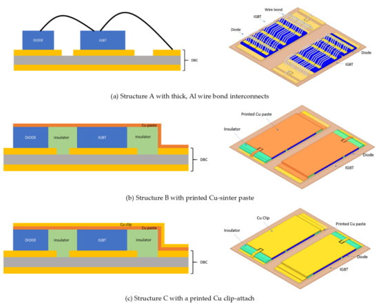
Figure 1.
Top-side interconnect structures: (a) structure A with Al thick wire bond (b) structure B with printed Cu sinter-paste, (c) structure C with printed Cu clip-attach. (b,c) are two variations of “sinterconnect” technologies.
2.1.1. Structure A–Thick, Al Wire Bond Interconnections
An array of 12 thick Al wire bonds, each with a diameter of 300 µm, were fabricated between the IGBT and diode devices and DBC via a wedge–wedge wire bonder (TPT HB 30, Munich, Germany), as shown in Figure 1a.
2.1.2. Structure B–Printed Cu-Sinter Pasted Interconnection
A commercial micron-sized Cu sinter paste with 77–82 wt% metal loading (DM-CUP 50, Dycotec Materials Ltd., Calne, UK) was jet-printed in a drop-on-demand mode by using a modular micro-assembly station (Häcker Automation GmbH, Waltershausen, Germany) equipped with a jet valve dispensing unit (Vermes Microdispensing GmbH, Holzkirchen, Germany). As shown in Figure 1 and Figure 2a, DBC sub-assemblies were built upon. Figure 2b shows how, first, a dielectric layer was jet-dispensed to planarize key interconnection surfaces of the DBC sub-assembly. Then, as shown in Figure 2c, Cu layers were dispensed.
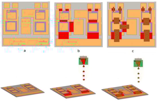
Figure 2.
Illustration of the jet-printing process flow for producing top-side Cu sinterconnects (a) multi-chip direct-bond-copper (DBC) sub-assembly, (b) jet-printing of dielectric paste, (c) jet-printing of copper paste.
To achieve constant line printing of the customized structures, position command data, in 2-D Gerber format, was manipulated such that the portal deposited paste every 250 µm. To consistently print lines of material deposit droplets, the droplet diameter was specified to be between 250 and 300 µm. Since the dynamic viscosity of the printed Cu paste was about 50,000 Pa-s, the paste was pre-heated to 70 °C to reduce viscosity to about 5000 Pa-s. The nozzle diameter was 200 µm. After printing, the Cu paste was dried at 80 °C for 20 min in an open-air atmosphere. The sintering of the Cu-paste was subsequently performed in a reflow oven at 200 °C under a formic acid atmosphere.
2.1.3. Structure C–Printed Cu Clip-Attach Interconnection
In this case, Cu-Paste was firstly jet-dispended on the contacting pads on the DBC sub-assembly and dried at 80 °C. The 100 µm-thick Cu foils were laser-cut to match the top-side layer’s topography. Then, Cu pieces (denoted as clips) were cleansed, with 4 vol% hydrochloric acid solution, for 10 s to ensure removal of contaminants and oxidized surfaces. The foils were eventually picked up by a mechanical arm of a die-bonder machine (Finetech, Germany) and precisely positioned on top of the designated area. Sinter bonding was then applied under a formic acid atmosphere at 200 N and 200 °C for 20 min.
2.2. Post-Fabrication Inspection and Measurement
For optical interconnect characterization, cross-sectional scanning electron microscopy (SEM), using a Helios G4 instrument (ThermoFisher Scientific, Waltham MA, USA) and optical microscopy were performed. Results are shown in Figure 3. Further on, electrical characterization of the half-bridge, DBC sub-assemblies was performed using a variable DC supply VBus and a 4 Ω load resistor following the schematics in Figure 4. It was first confirmed that the low side and high side switches could be actuated (turned on/off). Static device collector-emitter forward voltage drops, Vce, and device load currents, Ice, were then measured, with results presented in the next section of this paper.
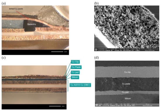
Figure 3.
Cross-sectional analysis of sinterconnects; structure B with printed Cu- sinter paste (a,b) and structure C with printed Cu clip-attach (c,d).
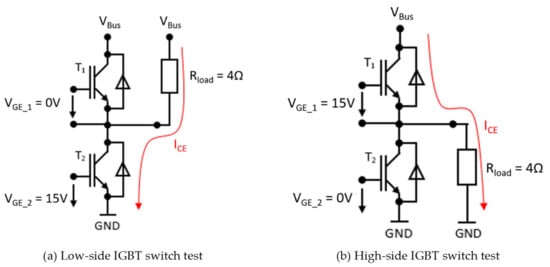
Figure 4.
Schematics of the electrical characterization of the half-bridge modules.
The thermal performance of the three structures was subsequently investigated and compared. In the test protocol, IGBT devices were turned on, with gate voltage Vge = 15 V. To manipulate the IGBT device conduction losses, the load current driven through each device was controlled via manipulation of the VBus setpoint shown in Figure 4. An infrared (IR) camera was used to measure the temperature response of the structures. For that, the top, exposed surfaces of the power devices were painted with matte black paint, enabling an approximation that that surface emissivity was near to unity.
2.3. FEM Simulations
In addition to the aforementioned experimental investigations, the electrical and thermal performances of sinterconnect structures were modeled to understand the characteristics of these structures at higher load currents (which were not feasible in the current lab set-up) and to optimize their material configurations. Here, several materials characterization techniques (e.g., electrical resistance measurements) were also utilized to enhance the simulation results.
2.3.1. Electrical Simulations
A comparative investigation of the power losses between a traditional, wire-bonded structure and the proposed sinterconnects was done using finite element (FE) simulation. Here, the FE environment Ansys Maxwell [25] was used to solve the macroscopic Maxwell equations in the electrostatic (DC conduction) and magneto quasi-static (Eddy current) regimes. Simulation convergence is granted by a mesh-refinement based iteration to reduce a global energy error and an energy variation between subsequent iteration steps. In all simulations target values of 1% global error and 1% energy change were undercut in two subsequent iteration steps as break-off criterion. For this characterization, the 1–100 kHz frequency range was analyzed as it lies close to pulse-width modulation switching frequencies employed by end-users of the power module. Analyses were completed for the constant, 100 A load current operating point. Ohmic losses were computed via the resistance R in the electrostatic approximation, with the corresponding AC losses represented by (1) in which Irms = I/√2 ≈ 71 A [26].
To quantify the effect of clip thicknesses, three different Cu thicknesses (i.e., 50, 100 and 200 µm) were simulated, whereas the thickness of the Cu sinter paste was set to be constant at the measured value of 124 µm. In the simulations, standard electrical resistivities for Cu (ρCu = 1.68 × 10⁻⁸ Ωm) and Al (ρAl = 2.63 × 10⁻⁸ Ωm) were utilized. For the Si parts, the resistivity of highly doped Si (ρSi-doped = 1 × 10⁻⁵ Ωm) was used. The electrical resistivity of the Cu paste was measured via 4-point probe tests and integrated into the model as 15.9 ± 1 × 10⁻⁸ Ωm for structure B and 6.4 ± 1 × 10⁻⁸ Ωm for structure C. The insulating material was separately characterized and modeled as a dielectric with a relative permittivity ϵr = 5. For dielectric characterization, the DC leakage current test through the dielectric was performed at different temperatures with a supply voltage of 400 V for 60 s. The volume resistivity as a measure of leakage current was calculated to be 3.84 × 10⁷, 2.8 × 10⁵, and 2.3 × 10⁴ Ωm at room temperature, 150 °C, and 200 °C respectively. Additionally, the AC breakthrough voltage at 50 Hz was determined to be 8.16 kV at room temperature.
2.3.2. Thermal Simulation
ANSYS simulation software was also used for thermal simulations. Assumed isotropic material parameters of the simulation module are shown in Table 1. The thermal conductivity of Cu-sinter pastes was estimated from physical electrical conductivity measurements and the Wiedemann-Franz law [27]. Thus, the ratio of thermal conductivity to electrical conductivity, at a fixed temperature, was considered constant. By comparing the electrical resistivities of the pastes with the bulk Cu, it was estimated that the thermal resistivity of the sinter pastes in B and C were approximately 10 times and 4 times that of the bulk Cu, respectively.

Table 1.
Thermal conductivities of the materials used for simulation.
For the thermal simulation, the power semiconductor module consisted of one IGBT and one diode mounted on a DBC substrate. Based on commercial products, DBC substrates were defined to be composed of a ceramic tile (345 µm alumina Al2O3) with a 275 µm-thick sheet of copper bonded to both sides. The power loss of the IGBT chip was defined as 100 W, whereas the power loss of the freewheeling diode was assumed to be 0 W. The IGBT heat load is applied with volumetric heat generation. Convective and radiative heat transfer coefficients were applied to the top surfaces and wires. The ambient air temperature was set to 25 °C. The heat transfer coefficients were determined using the values for natural convection of 8 W/(m2K) for the horizontal plate and 47 W/(m2K) for the cylinder [28].
Due to the large power density of the IGBT module (over 40 W/cm2), a water-cooled system was presumed, where the DBC can be mounted on a liquid-cooled base [29]. For this thermal analysis, a large convective heat transfer coefficient of 5600 W/(m2K) was applied to the bottom of the copper substrate. The coolant temperature was set to 40 °C.
3. Results and Discussion
3.1. Characterization and Measurements
The cross-sectional images of structures B and C are shown in Figure 3. As seen, both B and C sinter paste layers are homogeneous with regular thickness all along the joint. Structure B exhibits a pressure-less sintered Cu structure with higher porosity. In structure C, during the clip bonding, the pressure was applied to the paste. As a result of this pressure-assisted process, a denser and more homogeneous layer was formed in C. In a previous study, the relationship between the sintering pressure and density of Ag sinter pastes was shown [30]. It is well-known that increased porosity diminishes thermal and electrical conductivities of sintered materials [31].
To generally characterize the conduction properties of the IGBT devices integrated in the DBC structures, the on-state voltage drop of the IGBTs, Vce(on), was measured as a function of the load. For the three investigated concepts, the resulting Figure 5 plots measured output characteristics [32]. In this plot, the curve slopes are the IGBT device on-state transconductance. These results demonstrate how the performance of both sinterconnect systems (B, C) approaches the performance of the wire-bonded system (A). As seen, there were no discernable differences between structures A and C, while structure B showed a marginal deviation within measurement resolution. Please note that, although the employed measurement instruments were rated for the voltage and current sensing having 1 mV and 1 mA resolutions, error bars displayed in Figure 5 correspond to uniform ±5% voltage and current sensing error to provide the reader with perspective. The output characteristics shown in Figure 5 include compensation for the consistent 20–25 mW stray resistance of the measurement setup, due in part to external interconnections to multimeter devices. Since this stray resistance was observed to be temperature stable and constant throughout experiments, the voltage drop of the IGBT device and local, die-level interconnects could be clearly observed to vary between 80–98% of the uncompensated, measured voltage drops, depending on the load level.
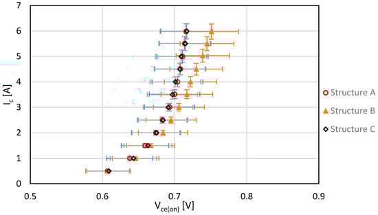
Figure 5.
Measured device output characteristics of the three structures.
Figure 6 shows exemplary photographs extracted from the IR camera during tests. It shows how temperature could be probed in a pixel-wise fashion. It also shows how rectangular selections were probed for maximum, average, and minimum temperatures. For the following results, average temperatures of the rectangular sections were used.
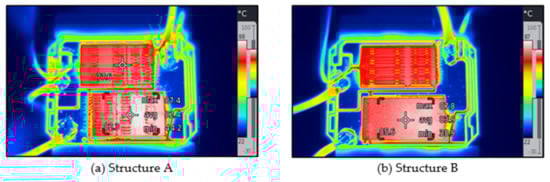
Figure 6.
Infrared thermographic images with load currents at (a) 6.2 A and (b) 6.4 A.
The three structures were benchmarked by incrementally increasing current, i.e., the conduction losses, and simultaneously measuring temperature. In Figure 7 the measurement results are plotted. It shows how ∆T, defined as the temperature difference between a measurement point and the ambient, increases as a function of the dissipated power losses.
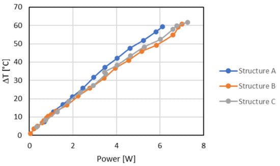
Figure 7.
Experimental measurement of ∆T temperature rise above ambient.
The predominantly linear trends visible in Figure 7 can be summarized by the single thermal resistance, Rth, parameter. Applying (2) to parameterize linear regression fits of the Figure 7 data allows for rapid, comparative assessment of the different structures’ thermal performances. Please note that, in (2), Ploss is the dissipated power losses, Tamb is the ambient temperature, and Tx is the measurement temperature taken from the IR camera.
Rth = ∆T/Ploss = (Tx–Tamb)/Ploss
Table 2 summarizes the apparent thermal resistances computed using (2). Like Figure 7, Table 2 suggests that sinterconnects (structures B and C) have relatively smaller Rth value.
Table 2.
Estimates of measured Rth based on measurement data.
All in all, the results of electrical and thermal measurements revealed that the sinterconnect structures exhibit similar performances to wire-bonded modules up to 7 W. None of the sinterconnect samples showed failures upon these measurements indicating that the printed samples could stand the electrical and thermal stresses without considerable cracking, delamination or severe oxidation.
3.2. Electrical and Thermal Simulation Results of the Sinterconnects at High Current Regimes
In the selected frequency range of interest, 1–100 kHz, eddy current contributions to the power losses were quantified, via finite element analysis, as negligible, compared to Ohmic losses. Weak eddy current influence was an expected behavior as the penetration depth is larger than the thicknesses of the conductive layers. Figure 8a shows the electrical resistances for the three top-side structures. Here, Cu sinter pastes with two extreme electrical conductivities were modeled. In particular, the ideal (ρCuPaste = 3 × ρCu) and the worst (ρCuPaste = 10 × ρCu) measured electrical conductivity values were simulated to perform a sensitivity analysis. Next, corresponding ohmic power losses computed according to (1) are reported in Figure 8b. The analysis predicts the superior performance of structure (C) compared with the other two systems.
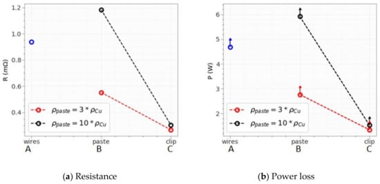
Figure 8.
Electrical simulation results of the ideal performances of the three structures in high-current regimes (a,b). The red lines refer to ρCuPaste = 3 × ρCu and the black lines to ρCuPaste = 10 × ρCu for a fixed tCuClip = 100 µm. Arrows in panel (b) show the maximum expected contribution at f = 100 kHz of eddy current effects on the power losses.
As inferred from this figure, when ρCuPaste = 10 × ρCu, the fully printed sinterconnects (structure B) exhibits higher losses than thick wire bonds. On the contrary, the sinter paste system with Cu clip (structure C) was rather consistent in both cases and was not highly influenced by the variation of paste conductivity. Structure C outperformed the wire-bond by a factor of two even in the worst scenario (i.e., ρCuPaste = 10 × ρCu). Given that, it can be deduced that even pressure-less Cu clip bonding can be considered as a promising top-side interconnect. Finally, in Figure 8b the arrows indicate the maximum expected variation at f = 100 kHz of the resistive power losses due to the contribution of eddy current effects.
A further investigation considering the effects of Cu clip thicknesses in structure C was carried out, where three clip thicknesses (tCuClip = 50, 100 and 200 µm) were compared. Figure 9 shows the resistance and the corresponding resistive power losses as a function of the tCuClip. Since the slope of power loss (P) depends on the ratio L/S where L is the length of the Cu clip and S is its cross-section, the system with tCuClip= 200 µm turned out to show the best performance with the least power losses. Like Figure 8, in Figure 9b, the arrows indicate the maximum expected variation at f = 100 kHz of the resistive losses due to the contribution of eddy effects. It is noteworthy to mention that, the unwanted presence of Cu oxide layer within Sinterconnect structures was estimated to add up to 3 × 10⁻⁴ Ω/um of thickness of the layer [33,34]. Therefore, the processing of sinterconnects under controlled atmosphere is crucial to acquire high performances.
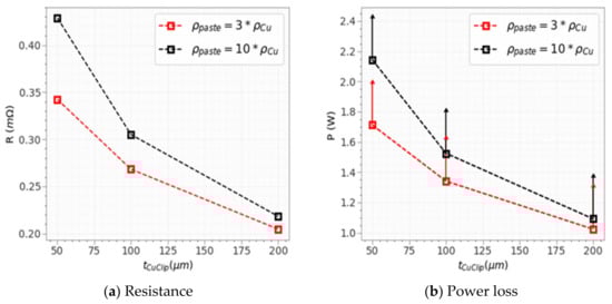
Figure 9.
Electrical simulation results of resistance (a) and power losses (b) as a function of tCuClip in structure C. The red lines refer to ρCuPaste = 3 × ρCu and the black lines to ρCuPaste = 10 × ρCu. Arrows in panel (b) once again show the maximum expected contribution at f = 100 kHz of eddy effects on the power losses.
Figure 10 shows the simulated temperature distributions for the three structures when dissipating 100 W. The maximum and average junction temperature (Tj) through the volume of an IGBT chip are reported in Table 3. One can notice from Table 3 that the maximum temperature of the module can be reduced by using the full area Cu contact provided by structures B and C. Structure C revealed the best performance. The difference between the thermal management of structures B and C was attributed to the difference in the porosity since voids inhibit heat conduction [35,36].
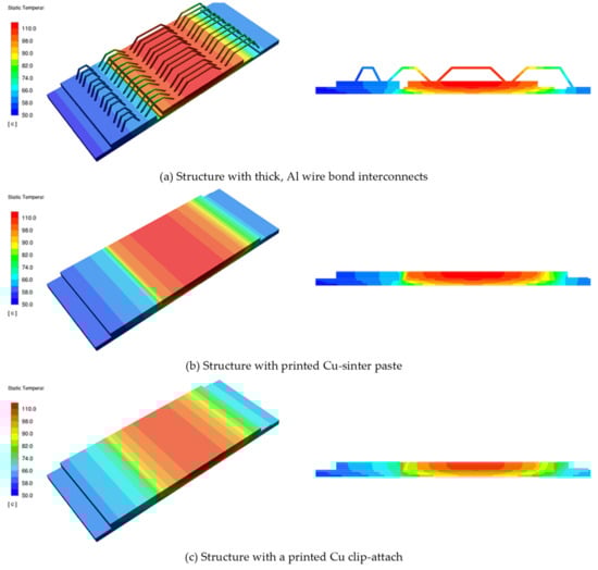
Figure 10.
Finite element-computed temperature distributions for the three presented structures at 100 W IGBT power dissipation.
Table 3.
Simulated Tj as a function of package structure (all units °C).
Nonetheless, by looking again at Table 3, the gained heat dissipation factor of structure C is not striking. This occurs since nearly 99% of the heat generated by the IGBT chip is transferred to the cooling liquid through the bottom surface. Therefore, the top-side interconnects in a single-side cooling technology cannot be a determining factor in terms of heat management. As a result, a follow-up thermal simulation of structure C was carried out with the assumption of a double-side cooling, where the water cooling was facilitated in both top and bottom sides. It can be clearly seen that the maximum temperature dropped to 74 °C. In fact, a principal benefit of the top-side planar interconnects in structures B and C is the possibility of implementing double-sided cooling for thermal management.
4. Conclusions
This paper investigated an implementation of copper sinter pastes as a basis for a fully printed interconnection system and as copper clip-attachment. The main difference between the two proposed sinterconnect concepts were the sintering conditions (pressure-less vs. pressure-assisted) yielding different porosity levels as well as the integration of a top Cu plate. The results of electrical and thermal measurement indicate the comparable I-V curves and Rth of all three structures up to around 7 W of IGBT device power dissipation. None of the sinterconnect samples showed pre-mature failures upon these measurements, indicating that the printed samples could withstand the electrical and thermal stresses without considerable cracking, delamination or severe oxidation. Furthermore, the electrical and thermal simulations at 100 W showed promising prospects that sinterconnects can outperform wire-bonded modules. According to simulation results, the sinterconnects with a thicker Cu clip can lead to lower resistive power loss. In addition, it was found that Cu-clip structure is not sensitive to the electrical conductivity of Cu-sinter paste. In the future, further examinations with higher voltages and currents up to 100 W as well as fast switching tests are planned to verify the actual performance of sinterconnects. Finally, thermal–mechanical reliability analysis is also an identified future work item.
Author Contributions
Conceptualization, A.R., A.B.; methodology, J.B., D.H., T.P., M.-H.M.; software, P.M., J.K.; validation A.R., T.P.; investigation, A.R., J.B., D.H., T.P., M.-H.M.; writing—original draft preparation A.R., P.M. and J.K.; writing—review and editing, A.B., T.P., M.O.; supervision, C.H., A.B.; project administration, A.R.; funding acquisition, A.B. All authors have read and agreed to the published version of the manuscript.
Funding
Power2Power is a European co-funded innovation project on Semiconductor Industry. The project receives grants from the European H2020 research and innovation program, ECSEL Joint Undertaking, and National Funding Authorities from eight involved countries under grant agreement No. 826417. The participating countries are Austria, Finland, Germany including the Free States of Saxony and Thuringia, Hungary, the Netherlands, Slovakia, Spain and Switzerland.
Institutional Review Board Statement
Not applicable.
Informed Consent Statement
Not applicable.
Data Availability Statement
Not applicable.
Acknowledgments
The authors gratefully acknowledges Richard Dixon and Aaron Chan from Dycotec Materials Ltd. for the material support.
Conflicts of Interest
The authors declare no conflict of interest. The funders had no role in the design of the study; in the collection, analyses, or interpretation of data; in the writing of the manuscript, or in the decision to publish the results.
References
- Hermanns, K.; Peng, Y.; Mantooth, A. The Increasing Role of Design Automation in Power Electronics: Gathering What Is Needed. IEEE Power Electron. Mag. 2020, 7, 46–50. [Google Scholar] [CrossRef]
- Broughton, J.; Smet, V.; Tummala, R.R.; Joshi, Y.K. Review of Thermal Packaging Technologies for Automotive Power Electronics for Traction Purposes. J. Electron. Packag. 2018, 140. [Google Scholar] [CrossRef]
- Yang, S.; Bryant, A.; Mawby, P.; Xiang, D.; Ran, L.; Tavner, P. An Industry-Based Survey of Reliability in Power Electronic Converters. IEEE Trans. Ind. Appl. 2011, 47, 1441–1451. [Google Scholar] [CrossRef]
- Oh, H.; Han, B.; McCluskey, P.; Han, C.; Youn, B.D. Physics-of-Failure, Condition Monitoring, and Prognostics of Insulated Gate Bipolar Transistor Modules: A Review. IEEE Trans. Power Electron. 2015, 30, 2413–2426. [Google Scholar] [CrossRef]
- Liu, K.; Yang, J.; Luo, J.; Wang, L.; Huang, Q.; Chen, F. The characterization and application of chip topside bonding materials for power modules packaging: A review. J. Phys. Conf. Ser. 2020, 1605, 012168. [Google Scholar] [CrossRef]
- Seal, S.; Mantooth, H.A. High Performance Silicon Carbide Power Packaging—Past Trends, Present Practices, and Future Directions. Energies 2017, 10, 341. [Google Scholar] [CrossRef]
- Durand, C.; Klingler, M.; Coutellier, D.; Naceur, H. Power Cycling Reliability of Power Module: A Survey. IEEE Trans. Device Mater. Reliab. 2016, 16, 80–97. [Google Scholar] [CrossRef]
- Wirebondless Semiconductor Package. U.S. Patent US8304903B2, 14 June 2006.
- Wirebondless Module Package. U.S. Patent US5616886A, 5 June 1995.
- Wirebondless Wafer Level Package with Plated Bumps and Interconnects. U.S. Patent US20090289356A1, 23 May 2008.
- Weidner, K.; Kaspar, M.; Seliger, N. Planar interconnect technology for power module system integration. In Proceedings of the 2012 7th International Conference on Integrated Power Electronics Systems (CIPS), Nuremberg, Germany, 6–8 March 2012; pp. 1–5. [Google Scholar]
- Zhu, Q.; Forsyth, A.; Todd, R.; Mills, L. Thermal characterisation of a copper-clip-bonded IGBT module with double-sided cooling. In Proceedings of the 2017 23rd IEEE International Workshop on Thermal Investigations of ICs and Systems (THERMINIC), Amsterdam, The Netherlands, 27–29 September 2017; p. 1. [Google Scholar]
- Barbarini, E.; Troadec, C. Power Module Packaging: Market and Technology Trends. In Proceedings of the Additional Conferences (Device Packaging, HiTEC, HiTEN, & CICMT), Boston, MA, USA, 30 September–3 October 2019; Volume 2019, pp. 749–779. [Google Scholar]
- Lee, H.; Smet, V.; Tummala, R. A Review of SiC Power Module Packaging Technologies: Challenges, Advances, and Emerging Issues. IEEE J. Emerg. Sel. Top. Power Electron. 2019, 8, 239–255. [Google Scholar] [CrossRef]
- Stockmeier, T.; Beckedahl, P.; Göbl, C.; Malzer, T. SKiN: Double side sintering technology for new packages. In Proceedings of the 2011 IEEE 23rd International Symposium on Power Semiconductor Devices and ICs, San Diego, CA, USA, 23–26 May 2011; pp. 324–327. [Google Scholar]
- Zhang, Z.; Chen, C.; Yang, Y.; Zhang, H.; Kim, D.; Sugahara, T.; Nagao, S.; Suganuma, K. Low-temperature and pressureless sinter joining of Cu with micron/submicron Ag particle paste in air. J. Alloy. Compd. 2019, 780, 435–442. [Google Scholar] [CrossRef]
- Jo, J.L.; Anai, K.; Yamauchi, S.; Sakaue, T. The Properties of Cu Sinter Paste for Pressure Sintering at Low Temperature. In Proceedings of the 2019 IEEE 69th Electronic Components and Technology Conference (ECTC), Las Vegas, NV, USA, 28–31 May 2019; pp. 76–80. [Google Scholar]
- Gao, Y.; Chen, C.; Nagao, S.; Suganuma, K.; Bahman, A.S.; Iannuzzo, F. Highly Reliable Package using Cu Particles Sinter Paste for Next Generation Power Devices. In Proceedings of the PCIM Europe 2019, International Exhibition and Conference for Power Electronics, Intelligent Motion, Renewable Energy and Energy Management, Nuremberg, Germany, 7–9 May 2019; pp. 1–4. [Google Scholar]
- Bhogaraju, S.K.; Conti, F.; Schmid, M.; Meier, M.R.; Schweigart, H.; Elger, G. Development of sinter paste with surface modified copper alloy particles for die-attach bonding. In Proceedings of the CIPS 2020 11th International Conference on Integrated Power Electronics Systems, Berlin, Germany, 24–26 March 2020; pp. 1–6. [Google Scholar]
- Gao, Y.; Li, W.; Chen, C.; Zhang, H.; Jiu, J.; Li, C.-F.; Nagao, S.; Suganuma, K. Novel copper particle paste with self-reduction and self-protection characteristics for die attachment of power semiconductor under a nitrogen atmosphere. Mater. Des. 2018, 160, 1265–1272. [Google Scholar] [CrossRef]
- Wei, T.B.; Khor, L.; Long, L.H.; Jeng, L.L.; Hang, G.S. Universal copper clip packaging solution for power management IC. In Proceedings of the 2015 China Semiconductor Technology International Conference, Shanghai, China, 15–16 March 2015; pp. 1–3. [Google Scholar]
- Zhu, Y.; Chen, H.; Xue, K.; Li, M.; Wu, J. Thermal and reliability analysis of clip bonding package using high thermal conductivity adhesive. In Proceedings of the 2013 IEEE 15th Electronics Packaging Technology Conference (EPTC 2013), Singapore, 11–13 December 2013; pp. 259–263. [Google Scholar]
- Hwang, J.S. Solder Paste in Electronics Packaging: Technology and Applications in Surface Mount, Hybrid Circuits, and Component Assembly; Springer: Berlin, Germany, 2012. [Google Scholar]
- Lwin, K.K.; Tubillo, C.E.; Panumard, T.J.D.; Suthiwongsunthorn, N.; Sirinorakul, S. Copper Clip Package for high performance MOSFETs and its optimization. In Proceedings of the 2016 IEEE 18th Electronics Packaging Technology Conference (EPTC), Singapore, 30 November–3 December 2016; pp. 123–128. [Google Scholar]
- ANSYS Electronics Desktop. 2019. Available online: https://www.ansys.com/products/electronics/ansys-electronics-desktop (accessed on 7 January 2020).
- Jackson, J.D. Classical Electrodynamics; Wiley: New York, NY, USA, 1999; pp. 1925–2016. [Google Scholar]
- Jones, W.; March, N.H. Theoretical Solid State Physics; Courier Corporation: Chelmsford, MA, USA, 1985; Volume 35. [Google Scholar]
- Gnielinski, V.; Kabelac, S.; Kind, M.; Martin, H.; Mewes, D.; Schaber, K.; Stephan, P. VDI-Wärmeatlas; Springer: Berlin, Germany, 2006; pp. 978–983. [Google Scholar]
- Qian, C.; Gheitaghy, A.M.; Fan, J.J.; Tang, H.Y.; Sun, B.; Ye, H.Y.; Zhang, G.Q. Thermal Management on IGBT Power Electronic Devices and Modules. IEEE Access 2018, 6, 12868–12884. [Google Scholar] [CrossRef]
- Kraft, S.; Zischler, S.; Tham, N.; Schletz, A. B3. 3-Properties of a novel silver sintering die attach material for high temperature-high lifetime applications. Proc. Sens. 2013, 2013, 242–247. [Google Scholar]
- Siow, K.S.; Lin, Y.T. Identifying the development state of sintered silver (Ag) as a bonding material in the microelectronic packaging via a patent landscape study. J. Electron. Packag. 2016, 138, 020804. [Google Scholar] [CrossRef]
- Baliga, B.J. Fundamentals of Power Semiconductor Devices; Springer: Berlin, Germany, 2010. [Google Scholar]
- Singh, B.; Mehta, B. Relationship between nature of metal-oxide contacts and resistive switching properties of copper oxide thin film based devices. Thin Solid Films 2014, 569, 35–43. [Google Scholar] [CrossRef]
- Nair, M.; Guerrero, L.; Arenas, O.L.; Nair, P. Chemically deposited copper oxide thin films: Structural, optical and electrical characteristics. Appl. Surf. Sci. 1999, 150, 143–151. [Google Scholar] [CrossRef]
- Katsis, D.; Van Wyk, J. Void-induced thermal impedance in power semiconductor modules: Some transient temperature effects. IEEE Trans. Ind. Appl. 2003, 39, 1239–1246. [Google Scholar] [CrossRef]
- Polom, T.A.; Van Der Broeck, C.H.; De Doncker, R.W.; Lorenz, R.D. Exploiting Distinct Thermal Response Properties for Power Semiconductor Module Health Monitoring. IEEE J. Emerg. Sel. Top. Power Electron. 2020, 1. [Google Scholar] [CrossRef]


Publisher’s Note: MDPI stays neutral with regard to jurisdictional claims in published maps and institutional affiliations. |
© 2021 by the authors. Licensee MDPI, Basel, Switzerland. This article is an open access article distributed under the terms and conditions of the Creative Commons Attribution (CC BY) license (https://creativecommons.org/licenses/by/4.0/).