Abstract
This paper focuses on the analysis and design of two multilevel–multicell converters (MMCs), named 3-phase 5-Level E-Type Multilevel–Multicell Rectifier (3Φ5L E-Type MMR) and 3-phase 5-Level E-Type Multilevel–Multicell Inverter (3Φ5L E-Type MMI) to be used in microgrid applications. The proposed 3-phase E-Type multilevel rectifier and inverter have each phase being accomplished by the combination of two I-Type topologies connected to the T-Type topology. The two cells of each phase of the rectifier and inverter are connected in interleaving using an intercell transformer (ICT) in order to reduce the volume of the output filter. Such an E-Type topology arrangement is expected to allow both the high efficiency and power density required for microgrid applications, as well as being capable of providing good performance in terms of quality of the voltage and current waveforms. The proposed hardware design and control interface are supported by the simulation results performed in Matlab/Simulink. The analysis has been then validated in terms of an experimental campaign performed on the converter prototype, which presented a power density of 8.4 kW/dm3 and a specific power of 3.24 kW/kg. The experimental results showed that the proposed converter can achieve a peak efficiency of 99% using only silicon power semiconductors.
1. Introduction
The electrical power demand has increased in all applications, such as transportation, industry, household, and the commercial sectors [1]. We are in fact becoming more and more hungry for electric power: on one hand, this is provoked by the constant increase in the world population, and consequently the urban centers are increasing in size with more people living in cities; on the other hand, the hunger for energy, especially in developing countries always in need of new infrastructure such as hospitals, schools, and transport, comes from the middle class. Thus, the increased demand of energy should be addressed by both significantly increasing the use of renewable energy sources and improving the efficiency of energy systems [2]. Currently, the most abundant renewable energy sources are wind and solar [3,4]; for both of them, adequate conversion equipment is needed. For example, wind energy requires turbines and generators, which leads to variable frequency and variable voltage electricity. As a result, between the generator and the grid, a power conversion system is needed in order to meet the grid requirement of a fixed frequency of 50 or 60 Hz at certain standard voltage levels. Concerning solar energy, a photovoltaic (PV) cell provides a DC source at unregulated low voltage, and thus power electronics systems must be able to adjust this DC voltage level to one suitable for supplying the load [5]. In the 21st century, therefore, modern solutions based on different energy sources coming from wind, solar, energy storage and micro-turbines have been used to feed the load or different loads [6,7]. Particularly, in a stand-alone microgrid, more energy sources are connected to a single DC-bus to supply the load, as shown in Figure 1. The photovoltaic system and the battery system are connected to the DC-bus thanks to a DC/DC power converter [8,9], while the wind system and the micro-turbine are connected to the DC-bus through an AC/DC converter. The power flows from the DC-bus to the load thanks to the DC/AC converter connected to a power filter.
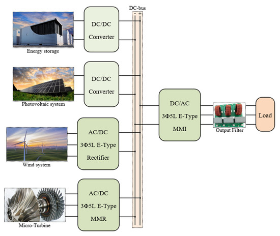
Figure 1.
Structure of stand-alone microgrid with the integrated renewable energy source.
It is evident that the modern renewable energy system could not operate, and the microgrid could not be realized, without power electronics. In fact, power electronics converters and controllers are the most important elements in this application, and the efforts of power conversion designers consistently focuses on improving the efficiency and reducing the volumes of the conversion system [10,11]. These goals can be reached thanks to the continuous improvement of power electronics technologies and power converter topologies. Indeed, on one hand the industrial manufacturing of power components keeps introducing new high-performance modules and power semiconductors on the market [12,13]; on the other hand, newer and emerging power converter topologies are constantly proposed in literature. For example, in high power and/or high voltage applications, the limit of the power conversion system is attributed to the power semiconductors capable of withstanding limited voltage and current stresses. To overcome this problem, academia and industry are working on new solutions of power converters [14,15,16]. Thus, the use of multilevel configurations allows the arrangement of power conversion systems with power semiconductors that are required to withstand only a fraction of both the overall DC-bus voltage and the converter output current. This usually allows higher switching frequency fsw and, therefore, multilevel configurations lead to significant improvements in terms of quality of both voltage and current waveforms without giving up the benefit of high efficiency and high-power density. Furthermore, the weight and volume of the converter passive components are likely to be reduced [14,15,16,17], which is very appealing for several applications, where the overall size and weight of the electrical generating system needs to be minimized. Given the high number of benefits, more and more multilevel converter topologies are proposed in the literature [17,18,19,20,21]. It is understood that multilevel topology can act on the voltage stress of the power semiconductors, leaving their current ratings unchanged. To reduce the current stress flowing through the power semiconductors, more parallel cell converters can be used. Thus, the power semiconductors with low current rating can be chosen, leading to an improvement in the conduction losses. As another advantage, parallel converters enhance the current ripple, resulting in a further improvement of the waveform quality. Obviously, the multilevel converters present some disadvantages, such as the reliability and cost. In fact, the number of power semiconductors in multilevel converters increases as the number of the voltage levels increases, and, therefore, we could think that cost and reliability worsen. However, some multilevel topologies proposed in the literature have fault tolerance capability [22,23,24]. Additionally, even if the number of power devices increases, there is a reduction in passive devices, which leads to less use of copper and iron. These materials, actually, are more expensive than power semiconductors. Naturally, the real disadvantage of having many devices could lie in the driver circuits used for switching the devices [25]. Moreover, tuning the control algorithm could also be more complicated, given the difficulty in finding an analytical model of the multilevel converter [26,27]. Nevertheless, apart from the analytical effort required to find the control law, the continuous trend of increasing the controller performance and memory size along with the reduction in the cost has now reached a point where the increase in the number of power semiconductors is not such a disadvantage. Multilevel converters based on Neutral Point Clamped (NPC) and T-Type topologies have been proposed using Super-junction MOSFETs [17,18]. Here, the peak efficiency is estimated to be above 99%. A five-level T-Type converter able to reach an efficiency of 99.2% using only SiC technology is presented in [19]. In this paper, the confirmed power density and specific power are 1.4kW/dm3 and 2.5kW/kg. In [20] a three-phase T-Type converter, called Swiss Rectifier, has been designed using SiC power devices. The declared peak efficiency and power density were 99.26% and 4 kW/dm3, respectively. A hybrid Five-Level Active NPC Inverter that uses SiC and is able to achieve a peak efficiency above 98% has been proposed in [21].
One of the goals of the proposed paper is analyzing, designing, and testing the 3Φ5L E-Type MMR and the 3Φ5L E-Type Multilevel–Multicell Inverter (MMI) to obtain high, efficiency, power density and specific power by using only silicon (Si) power semiconductors. For this purpose, the operation modes of the proposed converters are clearly explained and a solution to balance the DC-bus voltages is discussed. Then, the investigation focused on the design of the proposed converters; an analytical approach to calculate the device stress is presented to select the suitable power semiconductors. Starting from this analysis, the power semiconductors have been selected and the efficiency as a function of the power has been analytically calculated for both converters. The theoretical investigation has been supported by the model of the converters created in the Matlab/Simulink and Plexim/Plecs environments. A prototype of the converters has been built and the proposed MMR and MMI are integrated on the same power board to reduce the power density. Furthermore, the control structures for both MMR and MMI to be used in microgrid applications have been implemented and verified through preliminary simulations. Finally, experimental tests have been performed in order to confirm the obtained theoretical analysis. This paper is organized as follows: the topology, the operation principle, and the voltage unbalancing issue of the 3Φ5L E-Type MMR and 3Φ5L E-Type MMI are presented in Section 2. The hardware aspect design of the proposed rectifier and inverter are illustrated in Section 3. Based on the proposed rectifier and inverter, the control strategies regarding stand-alone microgrid applications have been discussed in Section 4. Simulation results and experimental results from a laboratory prototype are shown in Section 5 and Section 6, respectively. Conclusions are presented in Section 7.
2. Operation Structure of 3-Phase 5-Level E-Type MMC
2.1. 3Φ5L E-Type MMR and MMI
The circuit of the 3Φ5L E-Type MMR is illustrated in Figure 2. A single-phase of the rectifier has two cells: cell 1 and cell 2. This converter is based on both I-Type and T-Type topology [28,29,30]. In fact, each cell is composed of two I-Type legs connected to the T-Type leg. The power flows in one direction in the 3Φ5L E-Type MMR due to the presence of the diode into the T-Type cell. The two cells are connected in an interleaving manner, using an intercell transformer (ICT). The advantages of paralleling the cells using the ICT lies in the fact that the phase current is equally shared between the cells, the amplitude of the total current ripple is reduced, and the harmonic contents of the voltage at high frequency is shifted at twice the switching frequency. The 3Φ5L E-Type MMI is also composed of the I-Type and T-Type topologies like the rectifier, as illustrated in Figure 3. Each phase has two cells connected through the ICT.
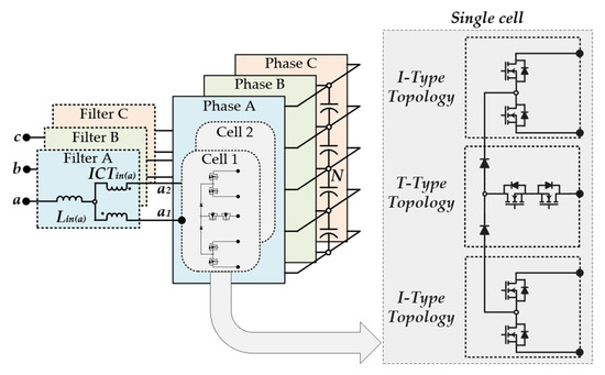
Figure 2.
Circuit of 3Φ5L E-Type Multilevel–Multicell Rectifier (MMR).
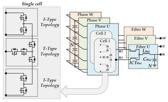
Figure 3.
Circuit of 3Φ5L E-Type Multilevel–Multicell Inverter (MMI).
According to the modulation control scheme, both converters show five voltage levels on a single cell, while each phase has nine voltage levels, as shown in Figure 4 and Figure 5. Thus, the line-to-line voltage shows seventeen voltage levels. A carrier-based pulse width modulation (PWM) method has been implemented, taking into account the multiple power semiconductors of the converters. The gate signals of the power devices are generated by the comparison of the modulating signals with the carriers, as shown in Figure 6. Considering the interleaving concept, a phase displacement is applied between the parallel cells in order to achieve highest quality of the output waveforms. Thus, four carrier signals, ct11, ct12, ct13 and ct14 (solid line) control the power devices in cell 1, and the other carrier signals ct21, ct22, ct23 and ct24 (dashed line) in the opposite phase control the power semiconductors in cell 2. Furthermore, as can be seen from Figure 6, two devices are controlled by a single carrier signal. The switching frequency of each power semiconductors is fsw while the output waveform effective switching frequency is twice fsw. This phenomenon, present in the interleaved converters, is usually called the multiplicative effect of the effective switching frequency, and leads to a drastic reduction in the output filter.
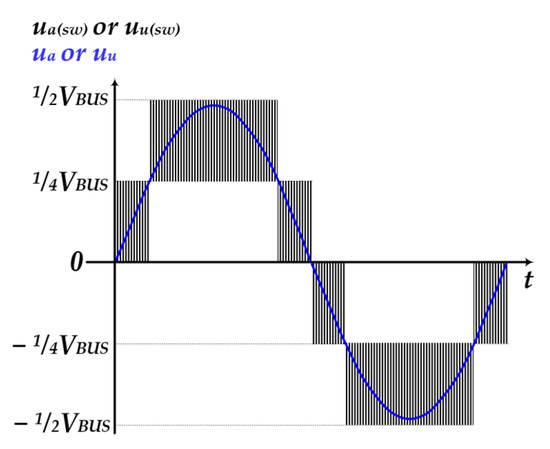
Figure 4.
Phase-to-neutral switching voltage ua1(sw) (or ua2(sw)).
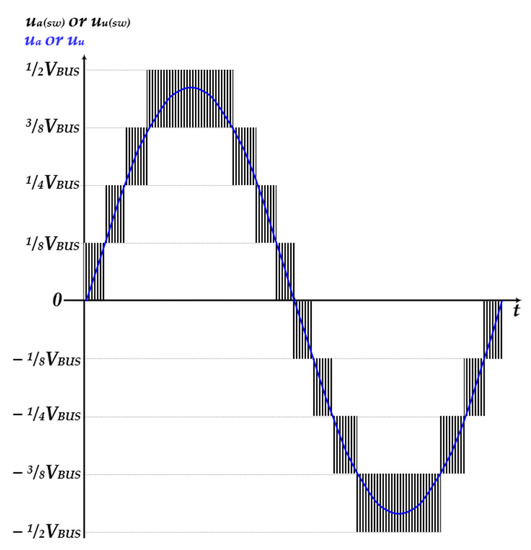
Figure 5.
Line-to-line switching voltage ua(sw) (or uu(sw)).
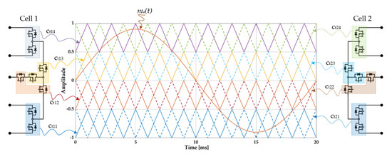
Figure 6.
Modulation control scheme for power semiconductors located in a single-phase of the inverter.
2.2. Balancing Circuit
The main problem of the multilevel converter based on T-Type or E-Type topologies is the unequal voltage across the DC-bus capacitors [31,32,33]. This problem cannot be solved in a simple way with a control algorithm due to the uncontrollable current flow through the internal nodes [28] of the capacitors. The only chance to balance the DC-bus capacitors of the 3Φ5L E-Type converters is to use an external circuit. The focus of this paper was not to study the unbalanced voltage capacitor problem. Here, two series resonant balancing circuits (SRBCs) have been used to solve the voltage unbalancing problem. Figure 7 illustrates the circuit and the implemented prototype of the SRBCs.
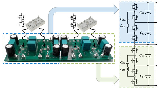
Figure 7.
Series resonant balancing circuit prototype.
The SRBCs were built with four Semitop3 SK75GB066T modules (rated 60 A—600 V), 4 µH and 16 µF as resonant total inductance (LR1/LR2) and total capacitance (CR1/CR2), respectively. Furthermore, one DC-bus film capacitor and two DC-bus electrolytic capacitors were used as a DC link. The energy was transferred from the capacitor CB1 to CB2 and from the capacitor CB3 to CB4 through the capacitors CR1 and CR2. The auxiliary inductors LR1 and LR2 were used to achieve a zero-current switching (ZCS) condition. The power semiconductors were driven with complementary control signals with a constant duty cycle at 50%; no control loops and sensors were required with the system being self-balanced. These two SRBCs were used to balance the voltage across the capacitors to ensure equal DC currents iC1 = iC2 = iC3 = iC4.
3. Hardware Design and Prototype of E-Type Topology
The 3Φ5L E-Type MMR and MMI have been designed to maximize the efficiency, power density, and specific power, without sacrificing the quality of the voltage and current waveforms. To accomplish these tasks, different actions have been carefully carried out.
The capacitors of the DC-bus have been chosen considering the maximum peak-to-peak voltage ripple ΔVBUS equal to 100 V and the estimated Root Mean Square (RMS) current flow through the capacitors in the case of an asymmetric load condition. The DC-bus current harmonics were compensated by the SRBCs except the 100 Hz component, which had to be compensated by the capacitors. For this reason, the DC-bus capacitors were selected according to (1), where NS and NP were the numbers of series and parallel capacitors, and ICBUS was the RMS current at double fundamental frequency defined in Equation (2).
In (2), U0 is the RMS voltage, I0 is the RMS load current, and VBUS is the total voltage across DC-bus capacitors. According to (1) and (2), six parallel and four series electrolytic capacitors, each one equal to 220 μF, 220 V were chosen as DC-bus capacitor tanks.
The power semiconductors were carefully selected considering the maximum voltage and current stress that the power components are able to withstand. Figure 8 shows the maximum voltage stress across the power semiconductors of a single cell of the inverter and rectifier.
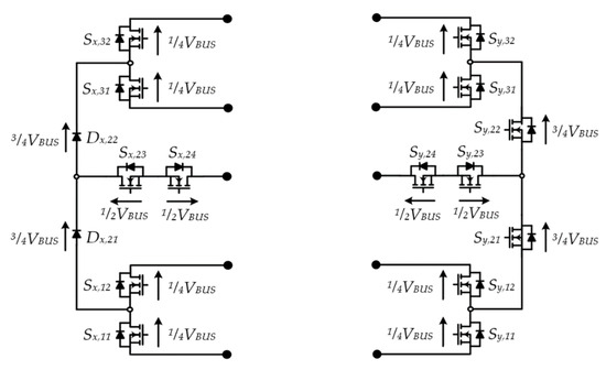
Figure 8.
Maximum voltage stress that each cell of the E-Type Rectifier and Inverter can withstand at a steady state.
As can be seen, the switches Sx,21, Sx,22 and the diodes Dx,21, Dx,22, with x ∈ {1R, 2R} and x ∈ {1I, 2I}, have the maximum voltage stress equal to 3/4VBUS compared to the other power semiconductors. Naturally, the overvoltage related to the commutated current must be added to this blocking voltage but, as explained in [34], the overvoltage commutation only appears when the blocking voltage at a steady state is equal to ¼VBUS. Concerning the current stress, the use of parallel cells helps to reduce the current stress of the power semiconductors. To obtain the current stress of each power semiconductors, an analytical procedure has been performed. Particularly, the average (AVG) and the root mean square (RMS) currents flowing in the power semiconductors located in the rectifier and inverter are expressed in Equation (3), where M0R is the modulation depth of the rectifier, Iin is the RMS phase current of the rectifier, M0I is the modulation depth of the inverter, I0 is the RMS phase current inverter, and aRMS,i, bRMS,i, aAVG,i, bAVG,i, aRMS,j, bRMS,j, aAVG,j, bAVG,j are the coefficients related to the switches of the rectifier (i-index) and inverter (j-index). The derivation of Equation (3) requires very complex analysis, and it is beyond the scope of this discussion. A simplified discussion to obtaining the Equation (3), including the coefficients, is discussed in detail in Appendix A.
Starting from this analysis, the selected power semiconductors of the 3Φ5L E-Type Rectifier and Inverter are listed in Table 1. To improve the power density and the specific power, the 3Φ5L E-Type MMR and MMI were integrated on the same power board. The power switches of the rectifier and inverter were driven by three boards, each one controlling a single-phase of the rectifier and inverter.

Table 1.
Power semiconductors used to build the 3Φ5L E-Type MMR and MMI with x∈ {1R, 2R} and y∈ {1I, 2I}.
The Infineon integrated circuit (IC) (part number 1EDI60I12AF) was employed as a gate driver chip. The printed circuit boards (PCBs) of the power board and the gate driver board have been optimized to reduce the current path during the commutations; in this way, the commutation inductance, i.e., the resulting inductance in the commutation circuit, has been reduced, and with it also the overvoltage commutation.
Additionally, because the high gate driver signals result from the high number of the power switches located in the 3Φ5L E-Type MMR and MMI, the interconnecting board which routes all the signals between the diver boards to the control board has been built.
Finally, the input and output filters have been designed to reduce the volume and to obtain high quality of the input currents in the rectifier side and high quality of the output voltages in the inverter side. Thus, the input and output ICTs and the input and output inductors have been built according to the analysis proposed in [30]. The complete prototype of the 3Φ5L E-Type MMR and MMI is illustrated in Figure 9, and features a power density of 8.4 kW/dm3 and a specific power of 3.24 kW/kg.
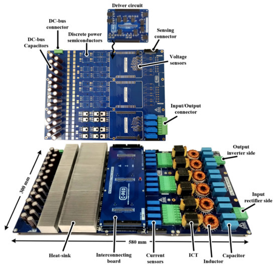
Figure 9.
Prototype of the 3Φ5L E-Type Rectifier and Inverter including the input and output power filters, measuring 580 mm × 300 mm × 45 mm. The power density is 8.4 kW/dm3 and the specific power is 3.24 kW/kg.
4. Control Interface
Figure 10 shows the block scheme of the 3Φ5L E-Type MMI. This converter must be provided with sinusoidal three-phase voltage waveforms with reduced total harmonic distortion (THDv). To meet this target, a multi-resonant controller [35] has been carefully chosen. Figure 11 illustrates the control algorithm of the 3Φ5L E-Type MMR connected to the wind source or to the micro-turbine source. As can be seen, the external speed loop provides the current reference to the q-controller inner loop. The task of this controller is to regulate the phase current to reduce the THD. The ICT circulating currents are regulated by adding an offset into the modulating signals with an additional loop.
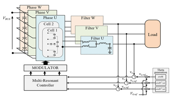
Figure 10.
Block diagram of the grid-side 3Φ5L E-Type MMI control algorithm.
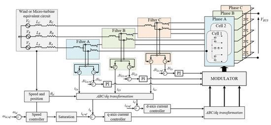
Figure 11.
Block diagram of the 3Φ5L E-Type MMR control algorithm for wind or micro-turbine sources.
5. Simulation Results
The hardware design previously addressed has been verified using a simulation model realized in the Matlab/Simulink and Plexim environments. Particularly, the power converter models have been implemented in Plecs, while the control structures have been implemented in Simulink. The stress of the power semiconductors and the losses distribution have been evaluated in the Plecs environment, which has a specific domain for modeling power semiconductors. Moreover, based on the manufacturer of the power semiconductors, the 2D look-up tables and 3D look-up tables have been created in Plecs to evaluate the loss distribution. Figure 12 and Figure 13 show the AVG and RMS current flowing into power semiconductors of the E-Type MMI and E-Type MMR for different values of the output power. Given the symmetry of the circuit, only the current flows through the power switches located in the bottom side of the E-Type MMI and E-Type MMR are illustrated. Both the analytical and experimental approaches provide the same results.
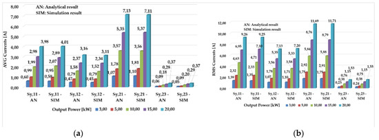
Figure 12.
Comparison between the analytical and simulation approaches of the currents flowing in the power semiconductors located in the 3Φ5L E-Type MMI: (a) average (AVG); (b) root mean square (RMS).
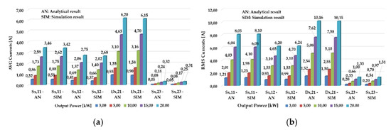
Figure 13.
Comparison between the analytical and simulation approaches of the currents flowing in the power semiconductors located in the 3Φ5L E-Type MMR: (a) AVG; (b) RMS.
As can be seen, in the inverter side the most stressed switches are Sy,21, Sy,22, while the least stressed switches are located in the middle leg Sy,23, Sy,24. In the rectifier side, the most stressed and the least stressed power semiconductors are Dx,21, Dx,22 and Sx,23, Sx,24, respectively.
Based on the datasheet provided by the power semiconductor manufacturers, it has been possible to estimate the efficiency distribution of the proposed converters using an analytical approach and a simulation approach. Particularly, starting from the achieved AVG and RMS currents, analytical equations to estimate the losses of the converters have been obtained according to the method proposed in [36]. Numerical efficiency results from the obtained analytical equations have been compared with simulation results. Figure 14 shows the total efficiency of the 3Φ5L E-Type MMR and MMI, including the passive components, as a function of the power. These results have been obtained based on the selected power semiconductors and the operating parameters listed in Table 1 and Table 2. The peak efficiency occurs when the power is close to 10 kW, while the efficiency at a nominal point is above 98%. As can be seen, the simulation results closely match the analytical results. Operation modes and characteristic waveforms of the 3Φ5L E-Type MMR and MMI have been evaluated according to the operating point listed in Table 2.
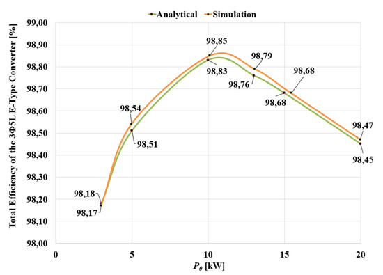
Figure 14.
Total efficiency of the 3Φ5L E-Type MMC as a function of the power P0: analytical result (green line), simulation result (orange line).
Table 2.
Operating parameters of the 3Φ5L E-Type MMR and MMI.
Figure 15 shows the output phase voltages uu, uv, uw, the phase-to-neutral switching voltages ua(sw), ub(sw), uc(sw), and the inductor phase currents iu, iu, iu of the 3Φ5L E-Type MMI under resistive three-phase loads. As can be seen, the voltage waveforms show a sinusoidal trend with very low total harmonic distortion.
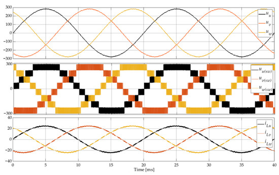
Figure 15.
Waveforms of the 3Φ5L E-Type MMI, from top to bottom: output phase voltages uu, uv, uw, phase-to-neutral switching voltages uu(sw), uu(sw), uu(sw), inductor phase currents iLu, iLv, iLw.
The waveforms of the 3Φ5L E-Type MMR are illustrated in Figure 16, where it is possible to notice, from the top to bottom, the phase back electromotive force (EMF) ua, ub, uc, the phase-to-neutral switching voltage ua(sw), ub(sw), uc(sw), the cell-to-neutral switching voltage ua1(sw), ub1(sw), uc1(sw), and the electrical machine phase current ia, ib, ic.
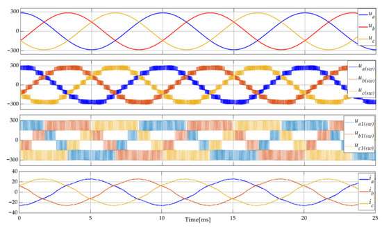
Figure 16.
Waveforms of the 3Φ5L E-Type MMR, from top to bottom: phase back electromotive force (EMF) ua, ub, uc, phase-to-neutral switching voltages ua(sw), ub(sw), uc(sw), cell-to-neutral switching voltages ua1(sw), ub1(sw), uc1(sw), electrical machine phase currents ia, ib, ic.
Here, the cell-to-neutral switching voltages also show five voltage levels, while the phase-to-neutral switching voltages exhibit nine voltage level. Thanks to the combination of the proposed topology and the control algorithm, the phase currents are regulated as three-phase sinusoidal waveforms with low total harmonic distortion.
6. Experimental Results
Experimental results have been carried out on 20 kVA 3Φ5L E-Type MMC prototypes previously described to support the proposed analysis. The DC-bus voltage was kept at 600 V by one port of the multi-port Dual Active Bridge (DAB) converter available in the laboratory [9]. The 3Φ5L E-Type MMR was connected to a permanent magnet synchronous motor (PMSM) to emulate the wind source and the 3Φ5L E-Type MMI was connected to the resistive load bench. Figure 17 shows the experimental setup of the multilevel converter including the SRBCs.
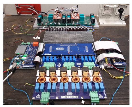
Figure 17.
Experimental setup of the 3Φ5L E-Type MMR and MMI.
As can be seen from the Figure 17, the 3Φ5L E-Type MMR and MMI were controlled using two different control boards, which were based on the National Instruments sbRIO-9651 System on Module (SoM), as shown in Figure 18. The SoM is equipped with both a microprocessor (μP) and a field-programmable gate array (FPGA), the control loop of the voltages or, in case of the rectifier side, the control loop of the currents and speed, run on the FPGA using 32-bit floating point arithmetic, while system managements and communication infrastructure are managed by the μP.
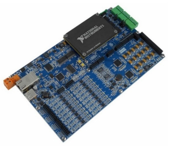
Figure 18.
Control architecture with the National Instruments sbRIO-9651 System on Module (SoM).
Figure 19 shows the phase-to-neutral switching voltage uu(sw), the cell-to-neutral switching voltage uu1(sw), the voltage waveform after the filter uu, and the phase current iu under resistive load, when the fundamental frequency f0 was equal to 50 Hz, the switching frequency fsw was equal to 20 kHz, and the modulation depth M0I was equal to 0.93. Figure 19 shows the five voltage levels across the single cell converter uu1(sw) and nine voltage levels across the single phase uu(sw) for a fixed modulation index. Figure 20 shows the output voltage waveforms under resistive load. These results prove the good capability of the multi-resonant controller to perfectly track the voltage references and to compensate the harmonics introduced by dead component time.
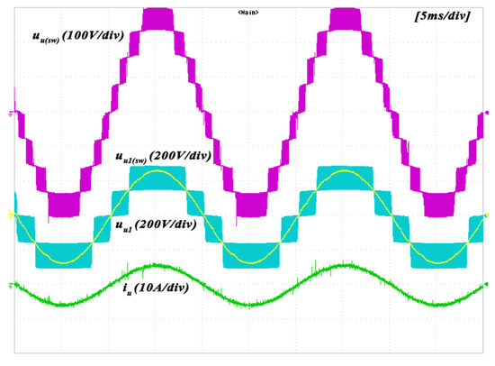
Figure 19.
3Φ5L E-Type MMI waveforms, from top to bottom: phase-to-neutral switching voltage uu(sw), cell-to-neutral switching voltage uu1(sw), output voltage uu and phase current iu.
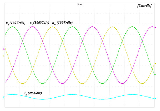
Figure 20.
Phase-to-neutral voltages uu, uv, uw of the 3Φ5L E-Type MMI side under resistive load.
Figure 21 illustrates the normalized harmonic spectrum of the phase-to-neutral voltage uu. The amplitude was normalized with respect to the fundamental. The harmonics magnitude from the 15th to 50th order exhibited an amplitude less than 0.1%. The THDv valuated up to the 50th order was close to 0.88%.
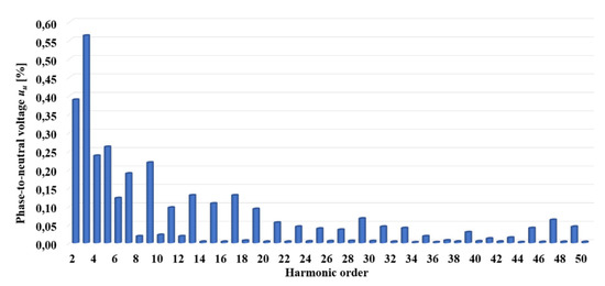
Figure 21.
Harmonic spectrum of the phase-to-neutral voltage uu.
Figure 22 shows the phase-to-neutral switching voltage ua(sw), the extracted fundamental component, the electrical machine phase current ia, and angular position θel, when the fundamental frequency f0 was equal to 100 Hz, the switching frequency fsw was equal to 20 kHz, and modulation depth M0R was equal to 0.93.
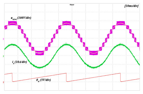
Figure 22.
3Φ5L E-Type MMR waveforms, from top to bottom: phase-to-neutral switching voltage ua(sw), fundamental component (extracted), electrical machine phase current ia, and angular position θel.
Here, the nine voltage levels are also clearly visible, and the control algorithm provided good tracking capability, making the machine current almost a pure sinusoidal waveform. The normalized harmonic spectrum of the phase current normalized with respect to the fundamental is shown in Figure 23. The THD of the electrical machine phase current estimated up to the 50th order was equal to 1.95%. The efficiency of the 3Φ5L E-Type Rectifier and Inverter have been evaluated by using the PM3000A wattmeter, where one channel has been used to measure the input power at the DC-bus and two channels have been used to measure the output power through Aron’s insertion. Figure 24 illustrates the experimental efficiency (blue line) of the 3Φ5L E-Type MMR plus 3Φ5L E-Type MMI including filters. As can be seen, the peak efficiency was equal to 98.81% by using only the Si power semiconductors, and at nominal power the efficiency was above 98%. Furthermore, the experimental results showed a good matching compared to the theoretical analysis. Consequently, the achieved experimental point validated the theoretical performance analysis of the 3Φ5L E-Type MMR and the 3Φ5L E-Type MMI.
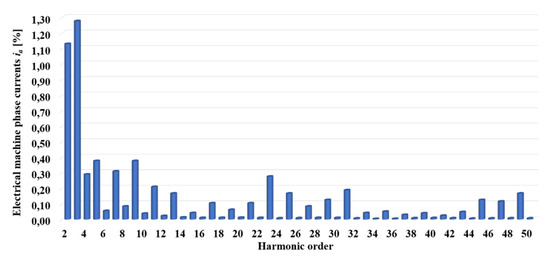
Figure 23.
Harmonic spectrum of the electrical machine phase currents ia.
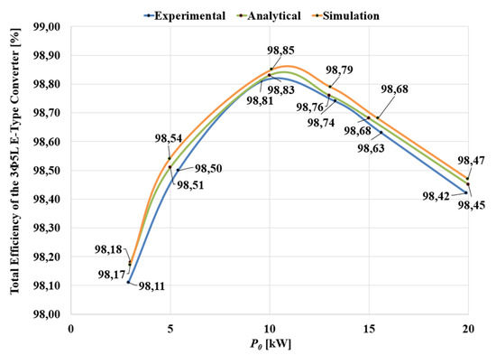
Figure 24.
Total efficiency of the 3Φ5L E-Type MMC as a function of the power P0: analytical result (green line), simulation result (orange line) and experimental result (blue line).
7. Conclusions
The multilevel–multicell 3Φ5L E-Type MMI and 3Φ5L E-Type MMR for stand-alone microgrid applications have been presented and discussed in this paper. The E-Type topology has been carefully studied with reference to the multicell interleaving configuration. The advantages and disadvantages of the proposed multilevel–multicell converters have been clearly explained. To build the prototype of the MMR and MMI, the hardware design process has been discussed. The prototype of the proposed multilevel-multicell has been built, aiming for improvements in the power density and specific power, as well as the power quality of the voltage and current waveforms. In fact, the complete prototype of the 3Φ5L E-Type MMR plus 3Φ5L E-Type MMI presented a power density of 8.4 kW/dm3 and a specific power of 3.24 kW/kg. To evaluate the performance of the multilevel–multicell converters, the control strategies have been introduced with particular regard to stand-alone microgrid applications. Experimental results confirmed the effectiveness of the proposed multilevel–multicell converters, achieving a peak efficiency of 98.81% using Si power semiconductors, as well as a THDv of 0.88% and a THDi of 1.95%.
Author Contributions
Conceptualization, P.J.G., and L.S.; methodology, F.C. and L.S.; software, M.d.B. and A.L.; validation, M.d.B. and A.L.; formal analysis, M.d.B. and A.L.; investigation, M.d.B.; resources, L.S., F.C. and A.L.; data curation, L.S. and A.L.; writing—original draft preparation, M.d.B.; writing— review and editing A.L., L.S., F.C. and P.J.G.; visualization, M.d.B.; supervision, L.S., A.L., F.C. and P.J.G.; project administration, L.S. and P.J.G.; funding acquisition, L.S., A.L., F.C. All authors have read and agreed to the published version of the manuscript.
Funding
This research received no external funding
Institutional Review Board Statement
Not applicable.
Informed Consent Statement
Not applicable.
Data Availability Statement
TNot applicable.
Acknowledgments
The authors are thankful to “Sky Research doo” for building the prototype of the multilevel converters, including the power filter used in the experimental campaign.
Conflicts of Interest
The authors declare no conflict of interest.
Appendix A
The analytical approach is presented in this section to calculate the AVG and the RMS current flowing through the power semiconductors in the 3Φ5L E-Type MMR and MMI. In general, the AVG and RMS current over one fundamental period can be found by Equations (A1) and (A2), where θ = ωt, ω is the fundamental frequency, i is the sinusoidal phase current, and dd is the duty cycle of the devices.
To find the RMS and AVG currents, the duty cycles of the power semiconductors in both rectifier and inverter must be obtained. According to the modulation strategy illustrated in Figure 6, the duty cycle of the devices can be derived from Equation (A3), where θin = ωint, θ0 = ω0t, ωin and ω0 the fundamental frequency of the rectifier and inverter, respectively, An,car is the amplitude of the carriers and mn,car is the offset of the carriers, with n = 1, 2, 3, 4, and mx(θin), my(θ0) are the modulation index of the rectifier and inverter, respectively, defined in (A4), with z ∈ {A, B, C} and w ∈ {U, V, W} and k = 0, 1, 2.
Substituting (A4) into (A3), the duty cycles for each power semiconductors in the single cell rectifier and inverter can be expressed as (A5) and (A6), where α1R = arcsin(0.5/M0R) and α1I = arcsin(0.5/M0I) are the angles between the carrier signals and the modulating signals of the rectifier and inverter, respectively. Replacing (A5) and (A6) into (A1) and (A2), and performing some algebraic manipulations, the RMS and AVG currents in each power semiconductors can be written as in Equation (3), where the coefficients aRMS,i, bRMS,i, aAVG,i, bAVG,i, aRMS,j, bRMS,j, aAVG,j, bAVG,j are listed in Table A1 and Table A2.
Table A1.
3Φ5L E-Type MMR power semiconductor coefficients of the RMS and AVG currents.
Table A2.
3Φ5L E-Type MMI power semiconductor coefficients of the RMS and AVG currents.
References
- Elavarasan, R.M.; Shafiullah, G.M.; Padmanaban, S.; Kumar, N.M.; Annam, A.; Vetrichelvan, A.M.; Mihet-Popa, L.; Holm-Nielsen, J.B. A Comprehensive Review on Renewable Energy Development, Challenges, and Policies of Leading Indian States with an International Perspective. IEEE Access 2020, 8, 74432–74457. [Google Scholar] [CrossRef]
- Ganesan, S.; Subramaniam, U.; Ghodke, A.A.; Elavarasan, R.M.; Raju, K.; Bhaskar, M.S. Investigation on Sizing of Voltage Source for a Battery Energy Storage System in Microgrid with Renewable Energy Sources. IEEE Access 2020, 8, 188861–188874. [Google Scholar] [CrossRef]
- Kesavan, T.; Sheebarani, S.; Gomathy, V.; Kavin, R.; Sivaranjani, S. Renewable Energy Based on Energy Conservation and Crossover System. In Proceedings of the 2020 6th International Conference on Advanced Computing and Communication Systems (ICACCS), Coimbatore, India, 6–7 March 2020; pp. 155–157. [Google Scholar]
- Guo, Z.; Wei, W.; Chen, L.; Dong, Z.; Mei, S. Impact of Energy Storage on Renewable Energy Utilization: A Geometric Description. IEEE Trans. Sustain. Energy 2020, 1. [Google Scholar] [CrossRef]
- Panigrahi, R.; Mishra, S.K.; Srivastava, S.C.; Srivastava, A.K.; Schulz, N.N. Grid Integration of Small-Scale Photo-voltaic Systems in Secondary Distribution Network—A Review. IEEE Trans. Ind. Appl. 2020, 56, 3178–3195. [Google Scholar] [CrossRef]
- Puchalapalli, S.; Tiwari, S.K.; Singh, B.; Goel, P.K. A Microgrid Based on Wind-Driven DFIG, DG, and Solar PV Ar-ray for Optimal Fuel Consumption. IEEE Trans. Sustain. Energy 2020, 56, 4689–4699. [Google Scholar]
- Salman, U.T.; Al-Ismail, F.S.; Khalid, M. Optimal Sizing of Battery Energy Storage for Grid-Connected and Isolated Wind-Penetrated Microgrid. IEEE Access 2020, 8, 91129–91138. [Google Scholar] [CrossRef]
- Mendola, M.L.; di Benedetto, M.; Lidozzi, A.; Solero, L.; Bifaretti, S. Four-Port Bidirectional Dual Active Bridge Converter for EVs Fast Charging. In Proceedings of the 2019 IEEE Energy Conversion Congress and Exposition (ECCE), Baltimore, MD, USA, 29 September–3 October 2019; pp. 1341–1347. [Google Scholar]
- di Benedetto, M.; Lidozzi, A.; Solero, L.; Crescimbini, F.; Bifaretti, S. Hardware design of SiC-based Four-Port DAB Converter for Fast Charging Station. In Proceedings of the 2020 IEEE Energy Conversion Congress and Exposition (ECCE), Detroit, MI, USA, 11–15 October 2020; pp. 1231–1238. [Google Scholar]
- Ebrahimzadeh, E.; Blaabjerg, F.; Wang, X.; Bak, C.L. Optimum Design of Power Converter Current Controllers in Large-Scale Power Electronics Based Power Systems. IEEE Trans. Ind. Appl. 2018, 55, 2792–2799. [Google Scholar] [CrossRef]
- Xu, Q.; Jiang, W.; Blaabjerg, F.; Zhang, C.; Zhang, X.; Fernando, T. Backstepping Control for Large Signal Stability of High Boost Ratio Interleaved Converter Interfaced DC Microgrids with Constant Power Loads. IEEE Trans. Power Electron. 2019, 35, 5397–5407. [Google Scholar] [CrossRef]
- Lazarević, V.Ž.; Zubitur, I.; Vasić, M.; Oliver, J.A.; Alou, P.; Patchin, G.; Eltze, J.; Cobos, J.A. High-Efficiency High-Bandwidth Four-Quadrant Fully Digitally Controlled GaN-Based Tracking Power Supply System for Linear Power Amplifiers. IEEE J. Emerg. Sel. Top. Power Electron. 2019, 7, 664–678. [Google Scholar] [CrossRef]
- Yuan, X.; Laird, I.D.; Walder, S. Opportunities, Challenges, and Potential Solutions in the Application of Fast-Switching SiC Power Devices and Converters. IEEE Trans. Power Electron. 2021, 36, 3925–3945. [Google Scholar] [CrossRef]
- Liang, G.; Tafti, H.D.; Farivar, G.G.; Pou, J.; Townsend, C.D.; Konstantinou, G.; Ceballos, S. Analytical Derivation of Intersubmodule Active Power Disparity Limits in Modular Multilevel Converter-Based Battery Energy Storage Systems. IEEE Trans. Power Electron. 2021, 36, 2864–2874. [Google Scholar] [CrossRef]
- Ebrahimi, J.; Karshenas, H. N-Tuple Flying Capacitor Multicell Converter—A Generalized Modular Hybrid Topology. IEEE Trans. Ind. Electron. 2019, 66, 5004–5014. [Google Scholar] [CrossRef]
- Meraj, M.; Bhaskar, M.S.; Iqbal, A.; Al-Emadi, N.; Rahman, S. Interleaved Multilevel Boost Converter with Minimal Voltage Multiplier Components for High-Voltage Step-up Applications. IEEE Trans. Power Electron. 2020, 35, 12816–12833. [Google Scholar] [CrossRef]
- McNeill, N.; Yuan, X.; Anthony, S.P. High-Efficiency NPC Multilevel Converter Using Super-Junction MOSFETs. IEEE Trans. Ind. Electron. 2015, 63, 25–37. [Google Scholar] [CrossRef]
- McNeill, N.; Yuan, X.; Jin, B. A Super-Junction MOSFET-Based 99%+ Efficiency T-Type Multilevel Converter. In Proceedings of the 2018 IEEE Energy Conversion Congress and Exposition (ECCE), Portland, OR, USA, 23–27 September 2018; pp. 5643–5650. [Google Scholar]
- Shi, Y.; Shi, Y.; Wang, L.; Xie, R.; Li, H. A 50 kW high power density paralleled-five-level PV converter based on SiC T-type MOSFET modules. In Proceedings of the 2016 IEEE Energy Conversion Congress and Exposition (ECCE), Milwaukee, WI, USA, 18–22 September 2016; pp. 1–8. [Google Scholar]
- Schrittwieser, L.; Leibl, M.; Haider, M.; Thöny, F.; Kolar, J.W.; Soeiro, T.B. 99.3% Efficient Three-Phase Buck-Type All-SiC SWISS Rectifier for DC Distribution Systems. IEEE Trans. Power Electron. 2019, 34, 126–140. [Google Scholar] [CrossRef]
- Zhang, L.; Zheng, Z.; Li, C.; Ju, P.; Wu, F.; Gu, Y.; Chen, G. A Si/SiC Hybrid Five-Level Active NPC Inverter with Improved Modulation Scheme. IEEE Trans. Power Electron. 2019, 35, 4835–4846. [Google Scholar] [CrossRef]
- Di Benedetto, M.; Lidozzi, A.; Solero, L.; Crescimbini, F.; Grbovic, P.J. Reliability and Real-Time Failure Protection of the Three-Phase Five-Level E-Type Converter. IEEE Trans. Ind. Appl. 2020, 56, 6630–6641. [Google Scholar] [CrossRef]
- Deng, F.; Lu, Y.; Liu, C.; Heng, Q.; Yu, Q.; Zhao, J. Overview on submodule topologies, modeling, modulation, control schemes, fault diagnosis, and tolerant control strategies of modular multilevel converters. Chin. J. Electr. Eng. 2020, 6, 1–21. [Google Scholar] [CrossRef]
- Pires, V.F.; Cordeiro, A.; Foito, D.; Pires, A.; Martins, J.; Chen, H. A Multilevel Fault-Tolerant Power Converter for a Switched Reluctance Machine Drive. IEEE Access 2020, 8, 21917–21931. [Google Scholar] [CrossRef]
- Omer, P.; Kumar, J.; Surjan, B.S. A Review on Reduced Switch Count Multilevel Inverter Topologies. IEEE Access 2020, 8, 22281–22302. [Google Scholar] [CrossRef]
- Benedetto, M.D.; Lidozzi, A.; Solero, L.; Crescimbini, F.; Grbovic, P.J. Low-Frequency State-Space Model for the Five-Level Unidirectional T-Rectifier. IEEE Trans. Ind. Appl. 2017, 53, 1127–1137. [Google Scholar] [CrossRef]
- Benedetto, M.D.; Lidozzi, A.; Solero, L.; Crescimbini, F.; Grbovic, P.J. Small-Signal Model of the Five-Level Unidirec-tional T-Rectifier. IEEE Trans. Power Electron. 2017, 32, 5741–5751. [Google Scholar] [CrossRef]
- Di Benedetto, M.; Solero, L.; Crescimbini, F.; Lidozzi, A.; Grbović, P.J. 5-Level E-type back to back power converters—A new solution for extreme efficiency and power density. In Proceedings of the 2017 13th Conference on Ph.D. Research in Microelectronics and Electronics (PRIME), Giardini Naxos, Italy, 12–15 June 2017; pp. 341–344. [Google Scholar]
- Di Benedetto, M.; Lidozzi, A.; Solero, L.; Crescimbini, F.; Grbovic, P.J. Five-level back to back E-Type converter for high speed gen-set applications. In Proceedings of the IECON 2016—42nd Annual Conference of the IEEE Industrial Electronics Society, Florence, Italy, 23–26 October 2016; pp. 3409–3414. [Google Scholar]
- Di Benedetto, M.; Lidozzi, A.; Solero, L.; Crescimbini, F.; Grbovic, P.J. Low Volume and Low Weight 3-Phase 5-Level Back to Back E-Type Converter. IEEE Trans. Ind. Appl. 2019, 55, 7377–7388. [Google Scholar] [CrossRef]
- Di Benedetto, M.; Lidozzi, A.; Solero, L.; Grbovic, P.J.; Bifaretti, S. ISOP DC-DC converters equipped 5-level unidirec-tional T-Rectifier for aerospace applications. In Proceedings of the 2015 IEEE Energy Conversion Congress and Exposition (ECCE), Montreal, QC, Canada, 20–24 September 2015; pp. 1694–1700. [Google Scholar]
- Cui, D.; Ge, Q. A Novel Hybrid Voltage Balance Method for Five-Level Diode-Clamped Converters. IEEE Trans. Ind. Electron. 2018, 65, 6020–6031. [Google Scholar] [CrossRef]
- Lin, H.; Shu, Z.; Yao, J.; Yan, H.; Zhu, L.; Luo, D.; He, X. A Simplified 3-D NLM-Based SVPWM Technique with Voltage-Balancing Capability for 3LNPC Cascaded Multilevel Converter. IEEE Trans. Power Electron. 2020, 35. [Google Scholar] [CrossRef]
- Di Benedetto, M.; Lidozzi, A.; Solero, L.; Crescimbini, F.; Grbovic, P.J. Five-Level E-Type Inverter for Grid-Connected Applications. IEEE Trans. Ind. Appl. 2018, 54, 5536–5548. [Google Scholar] [CrossRef]
- Lidozzi, A.; Di Benedetto, M.; Bifaretti, S.; Solero, L.; Crescimbini, F. Resonant Controllers with Three Degrees of Freedom for AC Power Electronic Converters. IEEE Trans. Ind. Appl. 2015, 51, 4595–4604. [Google Scholar] [CrossRef]
- Di Benedetto, M.; Lidozzi, A.; Solero, L.; Crescimbini, F.; Grbovic, P.J. Performance assessment of the 5-level 3-phase back to back E-type converter. In Proceedings of the 2017 IEEE Energy Conversion Congress and Exposition (ECCE), Cincinnati, OH, USA, 1–5 October 2017; pp. 2106–2113. [Google Scholar]


Publisher’s Note: MDPI stays neutral with regard to jurisdictional claims in published maps and institutional affiliations. |
© 2021 by the authors. Licensee MDPI, Basel, Switzerland. This article is an open access article distributed under the terms and conditions of the Creative Commons Attribution (CC BY) license (http://creativecommons.org/licenses/by/4.0/).