Article

Variable Speed Drive DC-Bus Voltage Dip Proofing

School of Electrical and Information Engineering, University of the Witwatersrand, Johannesburg 2000, South Africa
*
Author to whom correspondence should be addressed.
Energies 2021, 14(24), 8257; https://doi.org/10.3390/en14248257
Submission received: 7 October 2021 / Revised: 15 November 2021 / Accepted: 16 November 2021 / Published: 8 December 2021
(This article belongs to the Special Issue Power Electronic Converters: Control and Applications)

Abstract

:
This paper proposes a power electronic module that uses a switched capacitor for retaining the integrity of the dc-link voltage of a variable speed drive (VSD) during a 0.2 s short-term power interruption (STPI). Ride-through was achieved through switched capacitor onto the dc bus. However, this technique presents a challenge of the high inrush currents during a ride through compensation. In this work both analytical and experimental investigations were conducted in order to reduce the in-rush currents and its impact on the performance of the VSD during the STPI. Inrush peak currents were reduced by approximately 90%. Experimental results showed torque pulsations of 12.8% and 14.3% at the start and end of dc-link voltage compensation, respectively. A method for sizing the switched capacitor and the inrush limiting resistors is proposed. This methodology is based on the use of readily available nameplate information of the VSD and the electric motor. The proposed module can be retrofitted to existing VSDs that are based on v/f control.

1. Introduction

Electricity supply in developing economies is characterized by low generation and dominated by frequent faults and outages owing to lack of financial resources, old infrastructure and poor maintenance [1,2,3]. Voltage dip sensitive equipment including variable speed drives (VSD) are negatively affected by such frequent faults and outages leading to voltage dip-related trips. This results in disruptions of critical processes, loss of production and revenue [4]. Various transmission grid codes have a common way of defining which grid disturbances have to be tolerated. They also specify frequency of occurrence of these disturbances. VSDs are used to drive critical processes in power generation equipment and they are required to be able to ride-through a 0.2 s short-term power interruption (STPI) [5,6]. Studies carried out by numerous researchers to analyse the behaviour of a VSD during a voltage dip, have identified the dc-link under voltage as the main reason for the VSD tripping during a voltage dip [7,8,9]. There is an abundant number of VSDs on the market of different makes and models which gives rise to differences in susceptibility and response to voltage dips and STPI [9]. Existing VSD topologies can be modified to enhance their ride-through capability. Most modifications to existing topologies would require close collaboration with different manufacturers to access design base technical information. Such arrangements present challenges due to intellectual property which is closely guarded by manufacturers and thus not readily available for access by users of VSDs. Modifications to the drives must then be limited to an electrical connection only between the existing VSDs and ride-through enhancing module. This results in limited options available for enhancing ride-through capability for existing VSDs.
A VSD with a passive front end diode rectifier has limited response possibilities during a voltage disturbance which makes it sensitive to voltage dips [10,11,12]. Reference [13] developed a stacked switched capacitor for energy buffer on the dc bus and developed a switching scheme for the buffer switches. Voltage fault ride through is achieved in [12] through the use of field-oriented control. Various researchers have investigated alternatives of improving the ride-through capability of a VSD to voltage dips [10,11,14,15,16]. These alternatives can be grouped into those that allow ride-through for a total loss of power under an STPI and those that do not. Invariably, those that can offer ride-through for a STPI incorporate an energy storage device. Several STPI ride-through improvement alternatives incorporating energy storage are available to provide the required additional dc-link power. These include either ordinary or super-capacitors, battery based back-up systems, flywheel based energy storage, motor-generator sets, storage based on super conducting magnetic energy and fuel cells [14,17,18,19,20].
The simplest alternative for improving STPI ride-through involves increasing the overall dc-link capacitance. Most VSDs are equipped with an electrolytic capacitor on the dc-link. This capacitor is used primarily for filtering the dc-link voltage, providing limited energy storage for a VSD to ride-through minor voltage dips and providing a low impedance path for high frequency inverter currents [19]. Typical capacitance values are between 75–360 µF/kW [15]. Although a larger capacitor is preferred in order to strongly hold the dc link voltage for longer during a STPI, big capacitance tend to cause harmonic pollution onto the supply.
To be able to ride through a STPI, a sufficient energy reserve is required. A variety of energy storage technologies are candidates for providing the required power during a STPI. Battery backup systems, supercapacitors, motor-generator sets, flywheel energy storage systems, superconducting magnetic storage and fuel cells are some examples of these technologies [7]. For low voltage (<1000 V), low power (10 kW) applications, ordinary capacitors, super-capacitors and batteries are suitable candidates [14]. A boost converter maintains the dc-link voltage to a set point during the dip. The boost converter can be connected to the dc-link of a VSD, but more commonly is connected in parallel to the VSD. It uses the remaining voltage during a dip, to supply the dc-link. They do not use an energy storage device. Boost converters can be integrated into new drives between the rectifier and the dc-link capacitors or retrofitted as an add-on module [11,14]. During a voltage dip, the boost converter will sense a drop in the dc-link voltage and begin to regulate the dc-link to a minimum voltage required by the inverter. However, when the supply is completely lost due to a fault, the boost converter loses capability for ride through dip voltage. This paper proposes the use of a switched capacitor onto the VSD dc bus for a 0.2 s STPI ride through capability. Since the additional capacitor is only introduced during a dc bus voltage dip the power quality of the supply is not compromised during the healthy supply of power to the VSD. The power electronic module used to switch the capacitor onto the dc bus is equipped with the necessary inrush current limiting technique. The impact of switching a capacitor onto the dc bus was investigated based on motor performance and the dc bus performance. The work also proposes power electronic module sizing methodology based on the motor and VSD nameplate data.
The paper is organized as follows, Section 2 provides the behavior of the VSD under STPI and Section 3 proposes dc-link voltage dip compensation module. Section 4 is concerned with proposed sizing methodology for voltage dip compensation module, Section 5 with simulation results and analysis, Section 6 with experimental results, Section 7 with the overall analysis of results, and Section 8 with the conclusion.

2. Variable Speed Drive under Short-Term Power Interruption (STPI)

A voltage dip or STPI on the incoming AC supply of a VSD causes a drop in the dc-link voltage. If supply restoration is delayed, this can lead to a low dc-link voltage protection trip. VSDs are equipped with protection mechanism to guard against low dc-link voltage in order to guarantee good control and avoid damage to equipment. A number of studies have been carried to assess the tolerance of VSDs to voltage dips and STPIs [5,10,21]. Results indicate that most VSDs are most sensitive to three-phase dips and STPIs, less sensitive to two-phase dips and least sensitive to single phase dips. To ride through a STPI will depend on the size of the VSD dc link capacitor. The challenge is that in several industries, VSDs were designed for certain STPI duration. A comparison of VSDs from different manufactures indicates that most VSDs can only survive a STPI of up to 0.05 s. The energy within a VSD-motor-load system during a STPI can be represented by (1),
E L = E c   +   E kin
where EL is the total load energy, EC is the energy supplied by the capacitor and Ekin is the kinetic energy in the rotating masses. During a STPI, the capacitor and rotating masses provide energy EL to the load, resulting in the reduction of capacitor voltage and motor performance. EL can be expressed as in (2),
E L = C 2 Δ V c 2 ( t ) + J l 2 Δ ω 2 ( t ) = t 1 t 2 T l ω δ t
where Tl is the load torque, Jl is inertia, C is the dc-link capacitance, VC is capacitor voltage, ω is speed of rotating assembly and t2–t1 is the duration of the STPI. From (2), it can be concluded that the behavior of a VSD during a STPI is influenced by three main parameters: C which determines the electric energy EC stored in the dc-link, Jl which determines the kinetic energy Ekin stored in the rotating parts and the motor load Tl. For the same load torque, a VSD with a large capacitance driving a load with a high inertia has a better chance of riding through a voltage dip as compared to lower capacitance and motor inertia.
At the end of the STPI, i.e., when supply is restored, large inrush currents can be experienced due to reduced VSD dc link capacitor voltage. If not controlled, this inrush current can cause nuisance tripping of protective devices, damage VSD components and cause undesirable torque pulsations. The magnitude of inrush current is largely dependent on the capacitor voltage at the end of the STPI. A lower capacitor voltage results in a higher inrush charging current. Low dc-link voltage protection is incorporated to ensure that the capacitor does not discharge excessively which would otherwise lead to high inrush currents. During initial powering, inrush current is limited by use of a pre-charge resistor based circuit [22].

3. Proposed DC-Link Voltage Dip Compensation

The proposed voltage dip compensating module (module) was developed to ensure a 0.2 s ride-through capability of a 1.5 kW VSD while striving to sustain demanded motor load. This work only focus on V/f controlled VSDs as they are predominantly used in industry. The proposed module was required to be active only during an STPI and when charging in order to minimize harmonic pollution onto the grid associated with an increased capacitance on the dc link. Ride-through requirements are listed in Table 1.
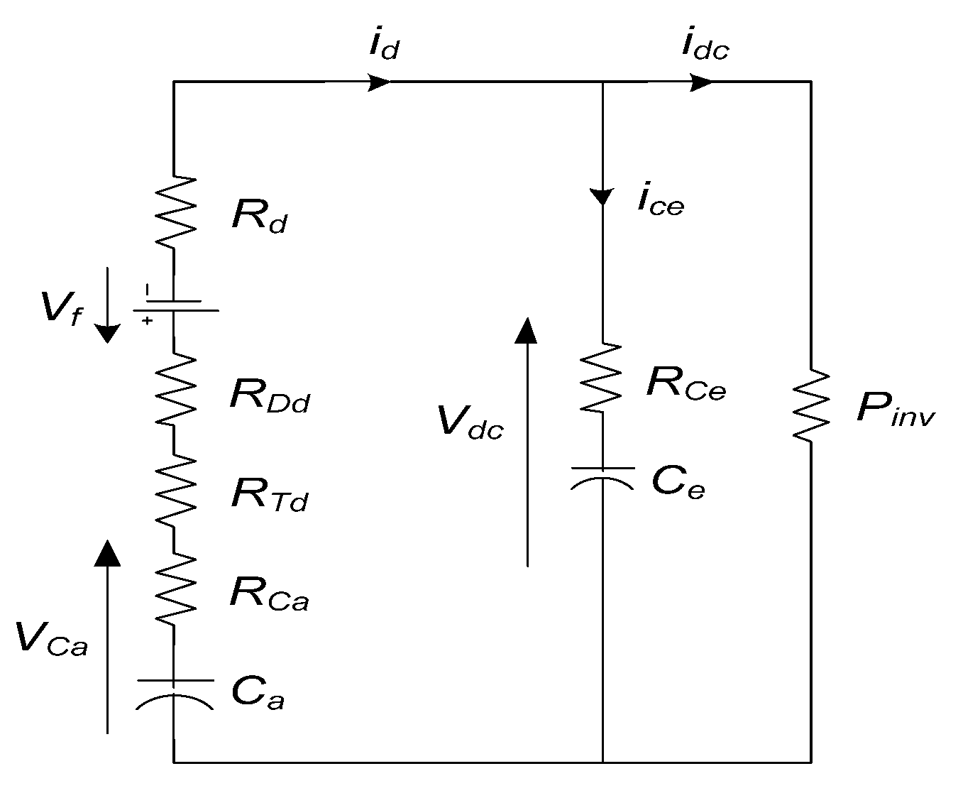
Figure 1 shows the proposed module developed for retaining the dc bus voltage using a switched capacitor Ca. Ce is the existing VSD dc bus capacitor. The switches Tc and Td controlled the charging and discharging of Ca, respectively. The diodes (Dc and Dd) were installed to prevent IGBT freewheeling diodes from conducting whenever the respective IGBT was switched off and thus allowed the flow of power in one direction in each of the charging and discharging circuits. The resistor RC, that was installed on the charging leg of Ca limited inrush current to be within VSD rectifier device ratings during charging of Ca. Resistor Rd installed on the discharging leg limited the inrush current when module was activated as Ca charged Ce.
Charging of Ca was conducted using the rectifier of the VSD through the dc bus. The detection circuit sensed the STPI and controlled the switching of IGBTs, Tc and Td which ensured that the voltage dip compensation module (VDCM) was switched onto the dc bus when required i.e., during the dip and taken out once the voltage STPI had cleared and Ca fully charged.

3.1. DC-Link during Compensation

Let us assume a low inertia load and a negligible energy contribution from rotating masses. During the period after the start of the STPI and before Ca is switched onto the dc-link, Ce provides energy required by the load. Thus, when Ca eventually is switched onto the dc-link, it charges up Ce and provides power to the load during the STPI. Figure 2 represents the dc-link during compensation. RCa is the capacitor internal resistance, RTd is the IGBTs on state internal resistance, RDd is resistance of the diode during conduction, Rd is the discharge current limiting resistor, RCe is the internal resistance of the VSD capacitor and Pinv is the VSD inverter input power. Relating capacitance and input power demand can be described in (3),
C = 2 P Δ t V Ca 2 V Ca _ min 2
where VCa and VCa_min are the capacitor voltages at start and end of compensation respectively, P is the total power demand and Δt is STPI duration, VCa can be represented as in (4) based on Figure 2,
VCa = id (RTd + RDd + Rd) + Vdc = VRdisch + Vdc
where VRdisch is the voltage drop across IGBT switch, diode Dd and resistor Rd. Substituting VCa from (3) into (4) results in (5),
C = 2 P Δ t V Ca 2 ( V dc min   +   V Rdisch   ) 2
Inrush current at start of compensation,
i d _ max = V c V d V f R Ca   +   R Td   +   R Dd   +   R d   +   R Ce
where Vdc is the dc-link voltage at start of compensation.

3.2. DC-Link during Charging

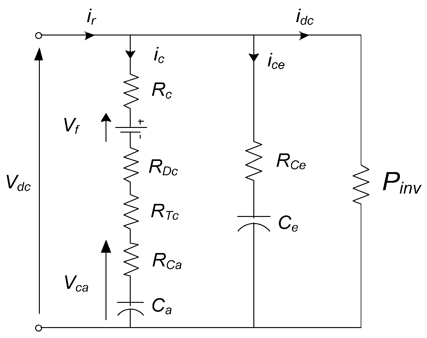
The DC-link during charging is shown in Figure 3, Inrush charging current ic at the start of charging can be obtained from (7),
Inrush charging current ic at the start of charging can be obtained from,
i c _ max = V dc V Ca _ min V f R Td   +   R Dd   +   R c
where VCa_min is the capacitor Ca voltage after compensation.

4. Sizing Methodology: Voltage Dip Compensating Module

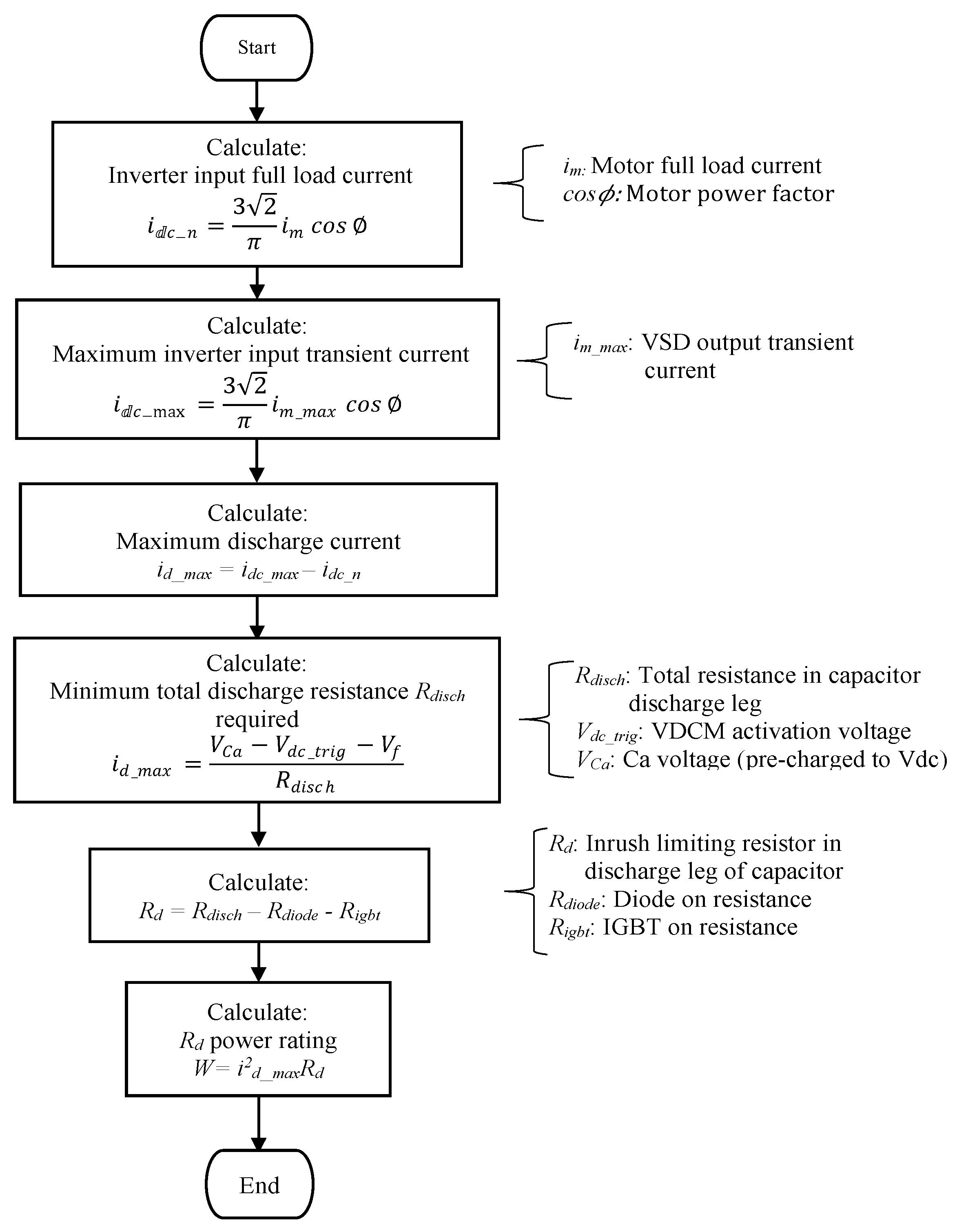
A sizing methodology based on readily available data such as the motor and VSD name plate information is developed. Figure 4, Figure 5 and Figure 6 show the proposed sizing methodologies for inrush current limiting resistors Rd, Rc and capacitor Ca. For Figure 4, this algorithm works backwards from motor size to the dc link of the VSD or inverter. The motor full load current and the motor power factor can be obtained from the motor name plate. These values will then be used to calculate the input inverter dc current (idc_n). The inverter output transient current or peak current can be obtained from the inverter nameplate. Once this is obtained the inverter peak dc bus current can be calculated (idc_max). Then this will allow for the maximum discharge current to be calculated (id_max). Since id_max will be calculated, and given a set voltage where compensation should start (Vdc_trig), diode forward voltage (Vf) and the capacitor voltage (Vca), it then becomes possible to calculate the total resistance in the capacitor discharge leg. Given the knowledge of the IGBT internal resistance and that of the diode, the current limiting resistor can then be calculated (Rd) including its power rating. Figure 4 shows the analytical progress of obtaining the size of the current limiting resistor when switching the additional capacitor onto the dc bus.
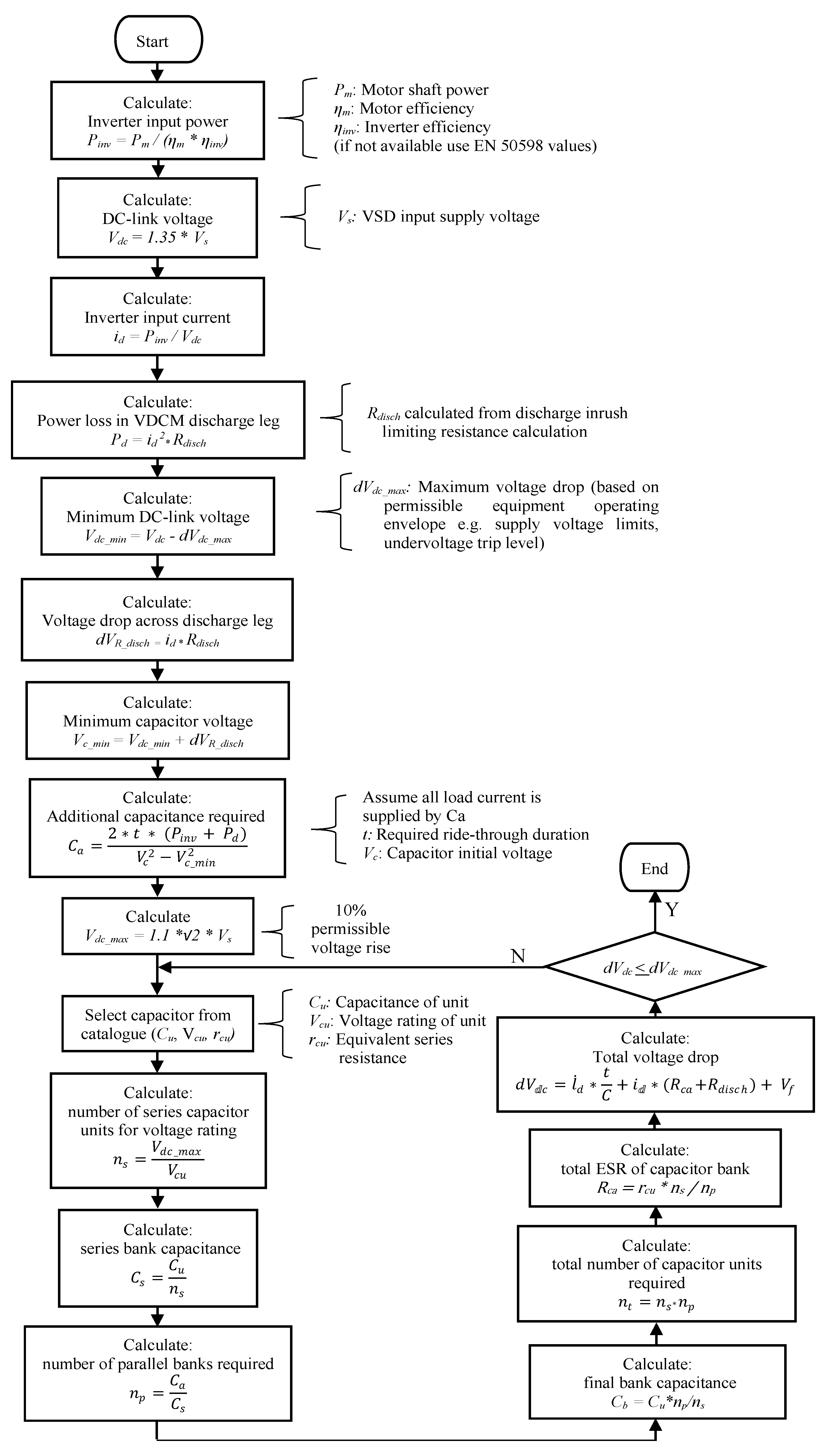
Figure 5 shows the additional switched capacitor sizing. Given the motor shaft power, motor efficiency and inverter efficiency from their nameplates the inverter input power can be calculated. The additional capacitor is calculated based on the assumption that full load current would be produced by this capacitor. This is because the additional capacitor will be used to supply the full load during a STPI. Given the known capacitance (from calculations) and the dc bus voltage, the appropriate capacitor can be chosen from the started capacitor units. Once the equivalent series resistor is calculated, the expected voltage drop on the dc bus can be calculated based on the chosen capacitor. If the voltage drop calculated is smaller than the set desired voltage drop (Vdc_max) then the loop ends. This will mean that the chosen standard capacitor will satisfy the conditions to not drop the dc bus voltage beyond (Vdc_max) during a STPI.
In Figure 6, a charging limiting resistor is calculated. Having obtained the VSD input inrush current by calculations. The rectifier maximum output current can be calculated. Once the minimum charging resistance is obtained, the inrush charging limiting resistor can be calculated including its power rating. It should be noted that during the charging scenario, the additional capacitor voltage would be minimal.
Sizing of the additional capacitor Ca and inrush current limiting resistors Rd and Rc was conducted for an induction motor with parameters shown in Appendix A, Table A1 and Table A2. Using the proposed sizing methodology, the calculated values for Ca, Rd and Rc obtained were 15.1 mF, 6.91 Ω and 8.15 Ω, respectively.

5. Simulation Results and Analysis

To validate the operation of the proposed module and assess its impact on VSD and motor behavior, simulation studies were carried out. The simulation model comprised a v/f PWM controlled inverter driving an induction motor rated at 1.5 kW. This study is only concerned with v/f control based VSDs. The VSD simulation parameters are listed in Table A3 in Appendix A.

5.1. Simulation Results without DC-Link Voltage Compensation

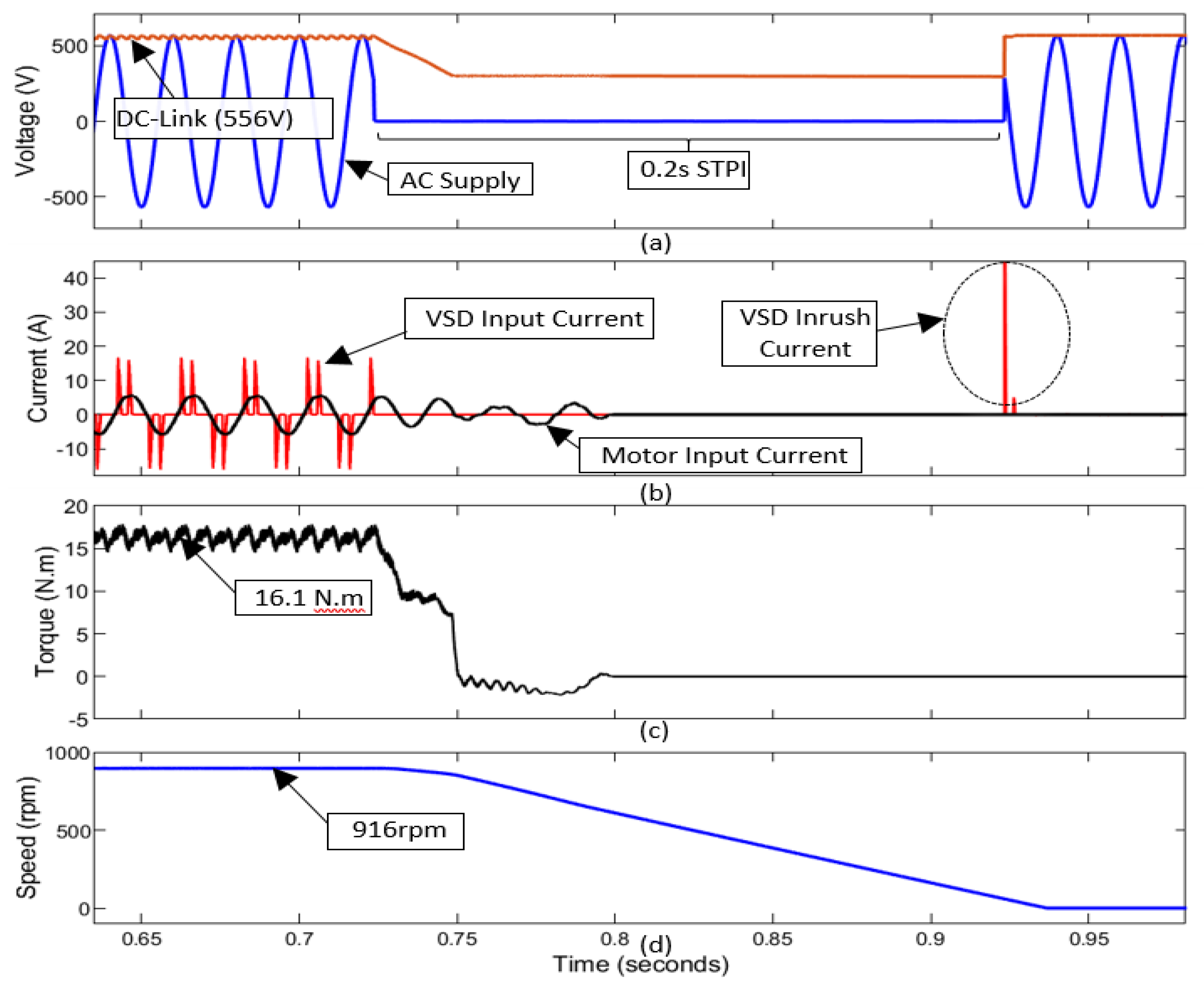
When a 0.2 s STPI was simulated on the VSD supply, the dc-link voltage started decaying at a constant rate from an initial value of 556 V whereas the dc-link capacitor of the VSD supplied all the power required by the motor as shown in Figure 7. There was a gradual reduction in speed and torque as the dc-link voltage decayed. The dc-link voltage continued to drop until 300 V which is the under-voltage trip setting at which stage the VSD tripped. This is indicated by the flattening of the dc-link voltage curve and a loss in motor torque. There was an increase in the rate of speed reduction as load torque decelerated the motor-drive rotating assembly. After VSD tripped, for a brief period, the motor switched to an induction generator as the load acted as the prime over and stator windings acted as a current source allowing self-excitation of the motor. Once stator current decayed to zero, developed torque decays to zero. After the STPI was cleared over a period of 0.2 s, there is a sudden buildup of inrush current as shown in Figure 7. This results from low resistance of the VSD capacitor which is now experiencing a sudden high voltage after the STPI.

5.2. Simulation Results with DC-Link Voltage Compensation

Figure 8 shows simulation results for the same 0.2 s STPI test with dc-link voltage compensation utilizing a 16 mF electrolytic capacitor bank.
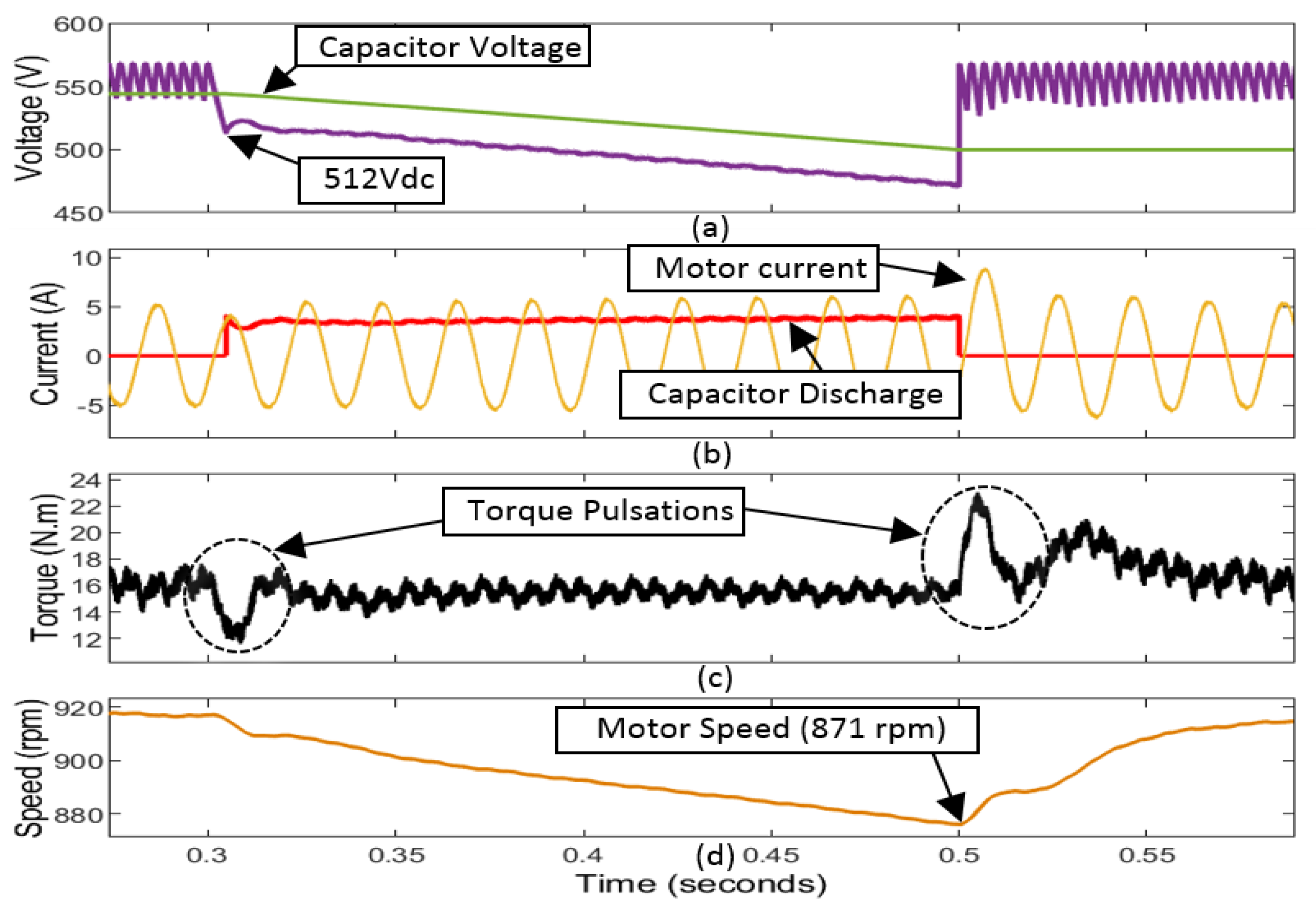
There was a decrease in the dc-link voltage when the supply was lost. At the point where the dc-link voltage dropped below the trigger set point voltage of 512 V, the dc-link voltage compensating device was initiated. The additional capacitor bank was switched onto the dc link and started supplying additional power. This is evidenced by the sudden halt in the “dc-link voltage” rate of decay and an increase in the dc-link voltage from 512 V to 524 V. The halting of the “dc-link voltage” decay was accompanied by a sudden increase of the current from the additional capacitor since the capacitor started to inject power into the dc-link i.e., delivering power to the motor as shown in Figure 8. Table 2 shows the summary of the simulation results.
The “dc-link voltage” continued to drop at a lower rate due to the influence of the additional capacitor. The start and end of compensation had a minor impact on the current drawn by the motor. There was, however, a steady increase in current drawn as the voltage decayed due to the need to maintain a constant power. Once supply was restored after 0.2 s and the “dc-link voltage” was retained from a minimum of 467 V to approximately 566 V, the capacitor bank was switched off from the “dc-link”.
Torque pulsations were observed when the compensating module was connected and disconnected respectively from the dc-link at STPI clearance. These torque pulsations were as a result of transients in the dc-link voltage at the start and end of compensation.
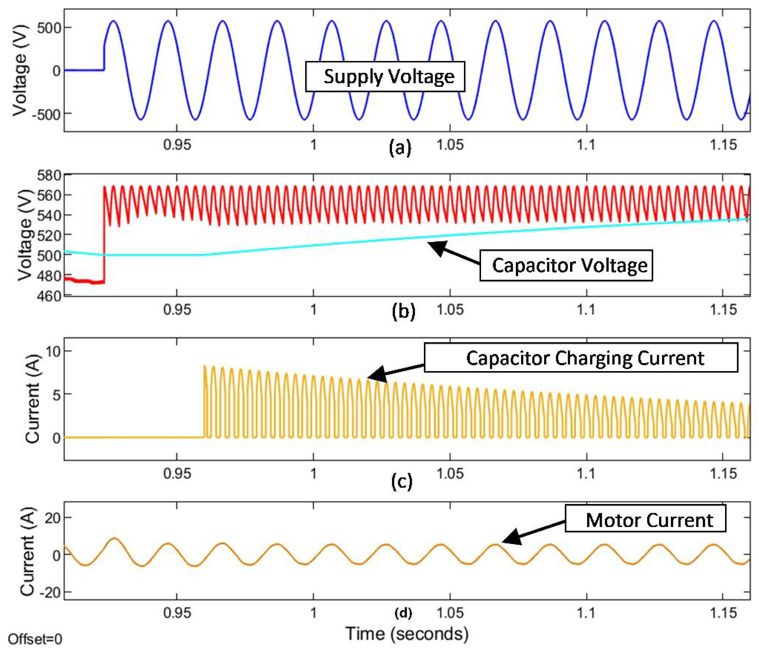
Once STPI had cleared and the dc-link voltage stabilized, charging of Ca from the dc-link commenced. Figure 9 shows the simulation results obtained. To avoid continuous and excessive loading of the dc-link due to charging action, pulse charging was adopted. This can be seen from the pulsed charging current trend. This approach resulted in minimum impact on the torque and speed of the motor.

6. Experimental Set-Up and Results

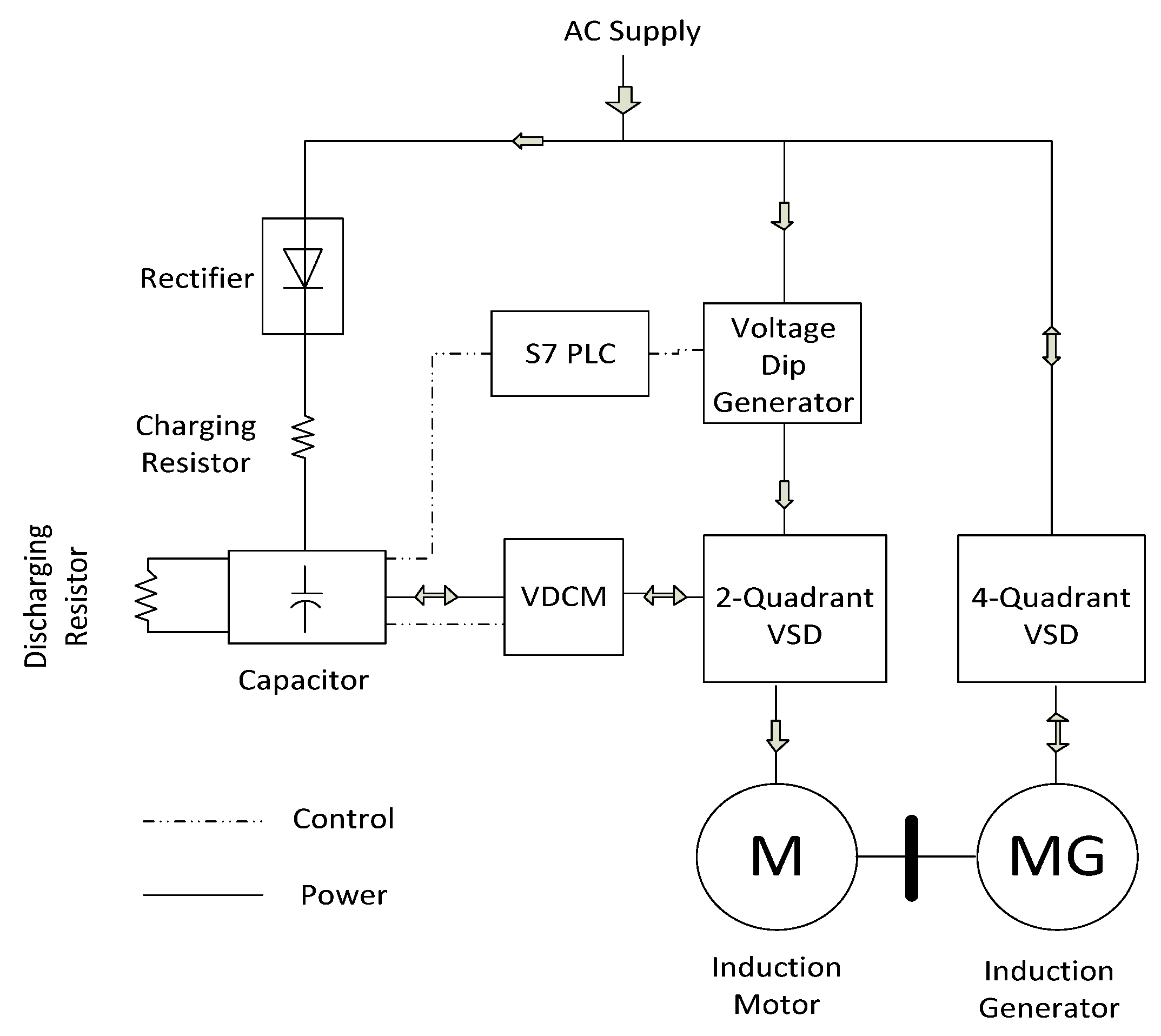
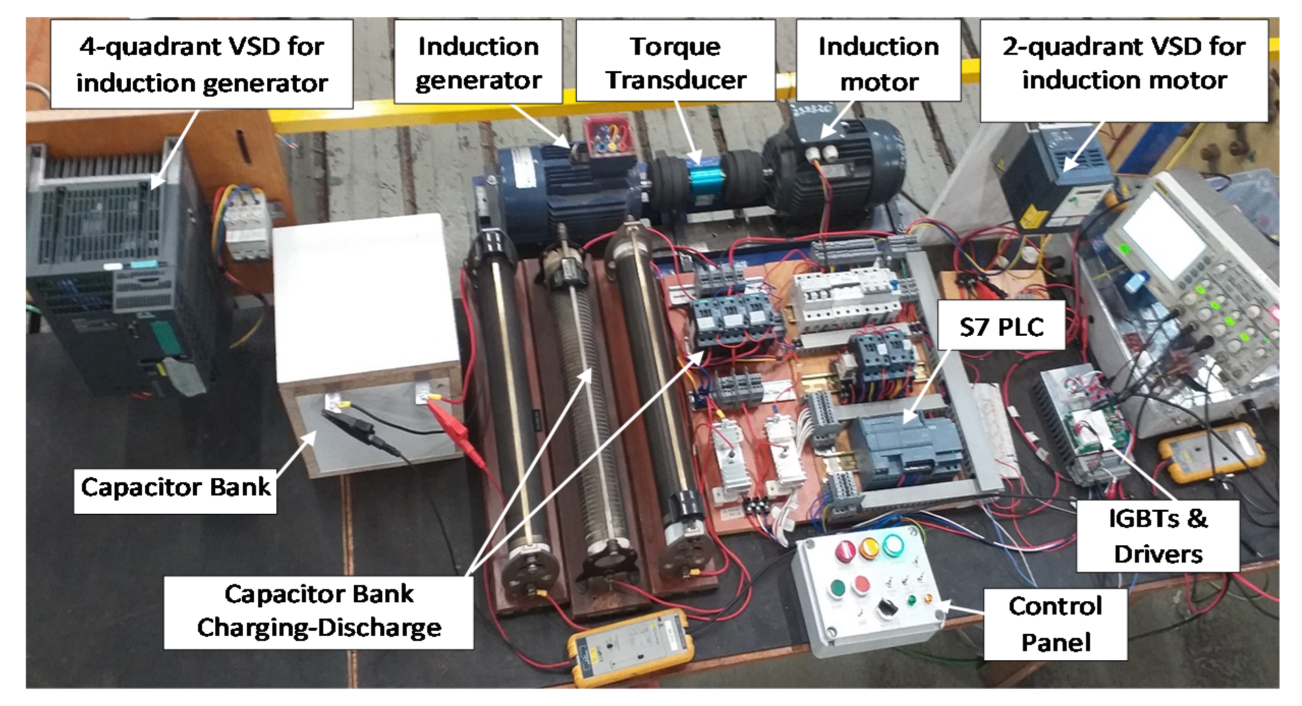
Two induction machines were used for the experimental setup. One machine acted as a motor and the other as a generator in order to load the induction motor. The motor was driven by two-quadrant industrial VSD. Loading on the induction generator was driven through the 4 quadrant VSD. Figure 10, shows the experimental block diagram. The proposed voltage dip compensating module (VDCM) was interfaced to a two-quadrant VSD connected to a 1.5 kW induction motor. A 2.2 kW induction generator coupled to the induction motor provided the required loading of the induction motor. The SIEMENS S7 Programmable Logic Controller (PLC) was used for the generation of the logic signals used for controlling the power switches. These power switches were responsible for creating a voltage dip on the dc bus and switching the additional capacitor onto the dc bus. Since a PLC was used for the generation of the switching signals, the period of the short-term power interruption could be set to any desired value.
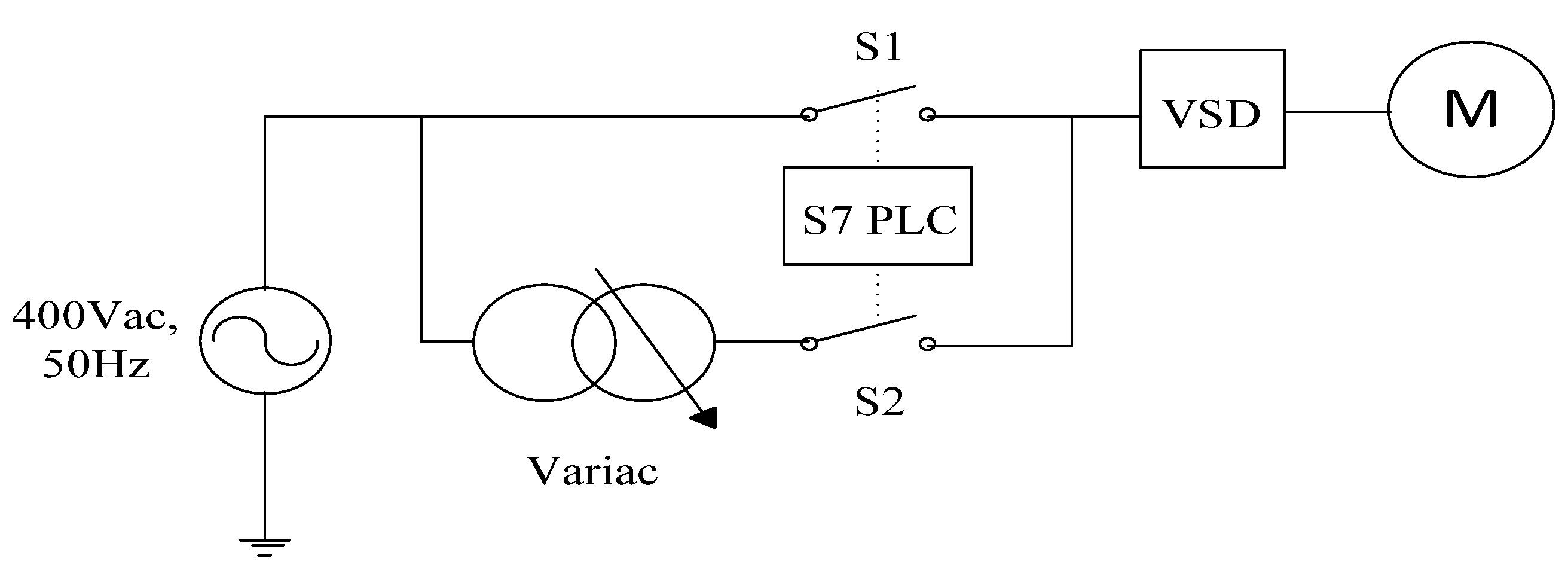
A variac transformer was used for the voltage dip generator on the dc bus of the 2 quadrant VSD. The variac allowed for any dc bus dip voltage needed to be achieved. Figure 11 shows the diagram of the voltage dip generator. When switch S1 is on S2 is open, the variac would be set to a lower supply voltage in order to emulate a fault on the supply and by switching on S2 for a particular period a voltage dip can be created on the dc bus of the VSD. Figure 12 shows the experimental set-up.
The motor speed and torque were measured by a torque transducer mounted between the motor and generator coupling. The torque transducer had a maximum error of 0.25%. The voltage transducers and the current transducers each had a maximum total error of +/−1%. Before the capacitor was put on standby for dc-link compensation, charging was carried out through a separately powered bridge rectifier as shown in Figure 12.

6.1. Experimental Test Conditions

The investigation involved assessing the behavior of the VSD without and with dc-link voltage compensation when subjected to a 0.2 s STPI. An industrial VSD was used and the investigation was carried out with the induction motor loaded to rated torque. To avoid damage to the VSD, key protection schemes including low dc-link voltage protection and overcurrent were left enabled. VSD dc-link voltage compensation, slip compensation and torque compensation control schemes were disabled to ensure alignment with the simulation model.

6.2. Results without “DC-Link Voltage” Compensation

Figure 13 shows the results obtained when the two-quadrant VSD is subjected to a 0.2 s STPI. Once supply to the VSD was lost, the dc-link voltage immediately started decaying as the VSD dc-link capacitor supplied all the required motor power. The VSD tripped once the dc-link voltage had dropped to below the low dc-link trip setting of 288 V. This is indicated by the flattening of the dc-link voltage curve. Once supply was restored at the end of the dip, the dc-link voltage rapidly increased to its nominal level with some initial oscillations. The voltage dip clearance was followed by a current spike as the VSD dc-link capacitor started charging up.

6.3. With “DC-Link Voltage” Compensation

The dc bus was operated at 556 V and the compensation capacitor was pre-charged to a voltage of 544 V as shown in Figure 14 and Figure 15, respectively. During a fault the dc bus voltage started to drop. Once the voltage drops below 512 V, the trigger circuit was activated which then effectively switched the additional capacitor bank onto the “dc-link”. Slight reductions in shaft speed including insignificant motor torque pulsations during the STPI were observed as shown in Figure 14. Figure 15 shows the instant increase of the discharge current from the additional capacitor drawn into the dc bus.

6.4. Compensation of Capacitor Charging from DC-Link

Figure 16 shows the results obtained of charging from the dc-link of the VSD. The charging circuit was configured to switch off once the dc-link voltage had dropped below a pre-set value. This was done to ensure that the dc-link was not excessively loaded by charging of the additional capacitor.
When charging was initiated, a considerable charging current was drawn, resulting in the dc-link voltage dropping below the charging threshold. This caused the charging IGBT to switch off. In this state, the dc-link voltage recovered resulting in the IGBT switching on. This repeated switching results in a pulsed charging current. Once the additional capacitor voltage had recovered to a value which did not trigger switching off the charging IGBT, continuous charging occurred till the capacitor was fully charged.

7. Analysis of Results

Table 3 summarizes the variations in the dc-link voltage and capacitor voltage during compensation.
The voltage drop across the capacitor is less than that of the dc-link. This is as a result of the voltage drop across the inrush limiting resistor during compensation. Table 4 shows the impact of the compensating module on torque and speed.
A comparison of key parameters from calculation as per proposed sizing methodology, simulation and experimental results are summarised in Table 5 and Table 6. There is a strong correlation between calculated values (as per sizing methodology), simulation and experimental results for the proposed voltage dip compensation.
To further test the proposed sizing methodology, a study was undertaken for a 7.5 kW motor. Data used for the 7.5 kW induction motor assessment is listed in Table A4 in Appendix A. The results of key parameters are shown in Table 7 and Table 8.
Calculated and simulated results for dc-link voltage compensation for a 7.5 kW induction motor during a STPI are very comparable. The proposed sizing methodology can thus be used for different sized motors which are driven from a v/f controlled VSDs.

8. Conclusions

This paper investigated and developed inrush current mitigation schemes for a proposed dc bus voltage ride through a power electronic module. The paper can be summarized as follows:
  • A switched capacitor can be used to improve voltage ride through for a dc bus voltage;
  • There was a torque pulsation of 12.8 and 14.3% at the start and end of dc-link voltage compensation respectively;
  • During voltage dip ride through (compensation) there was a 2.5% drop in the speed and 10.3% drop in the motor torque;
  • A sizing methodology for the additional capacitor and discharge limiting resistor has been tested and validated. This methodology uses readily available motor and VSD nameplate information;
  • The voltage ride through module was able to retain up to 82% of the dc bus voltage during 0.2 s STPI which avoided a trip on the VSD;
  • There was good agreement between simulations and experimental results and, when comparing the two, there was a 2.4% voltage difference on the dc link voltage drop and 2% difference on the switched capacitor voltage drop during compensation. There was a 2.4% difference between simulations and experimental work on the amount of the discharge current;
  • The proposed method whilst effective in improving ride-through capability of VSD resulted in an unwanted voltage drop and energy losses due to the inrush current limiting resistor, which led to reduced overall module efficiency;
  • The observed behaviour of the VSD was based on a STPI which presents the worst-case scenario. Improved behaviour is expected for less severe voltage dips;
  • The voltage compensation module can be added to existing VSDs that are based on V/f control in order to avoid operational breakdowns.

Author Contributions

F.C. contributed towards the write up of the paper, methodology, experimental work and validation. L.M. contributed towards the conceptualization of the research idea, review, editing of the paper, methodology and supervision. All authors have read and agreed to the published version of the manuscript.

Funding

This work was funded by the Eskom Power Plant Engineering Institute program and the national research foundation of South Africa under grant 118120.

Institutional Review Board Statement

Not Applicable.

Informed Consent Statement

Not Applicable.

Data Availability Statement

Not Applicable.

Acknowledgments

This project is part of the Eskom Power Plant Engineering Institute program at Wits University. Authors also acknowledge the support of the National Research Foundation of South Africa.

Conflicts of Interest

The authors declare no conflict of interest.

Nomenclature/Abbreviations

ELTotal load energy (Wh)
ECEnergy supplied by capacitor (Wh)
EkinKinetic energy in the rotating mass (Wh)
TLLoad torque (N.m)
ωSpeed of rotating assembly (rad/s)
JlInertia (kg·m2)
VcCapacitor voltage (V)
CaSwitched capacitor (F)
CeInvereter dc bus capacitance (F)
Vdcdc bus voltage (V)
Idcdc link current (A)
ISVariable speed drive supply current (A)
VsVariable speed drive supply voltage (V)
RcaInternal resistance of the switched capacitor (Ω)
RTdThe switch internal resistance (Ω)
RDdThe resistance of the diode during conduction (Ω)
RdThe discharge current limtting resistor (Ω)
RceThe internal resistance of the VSD capacitor (Ω)
PinvThe VSD inverter input power (W)
VCaInitial capacitor voltage
VCa_minCapacitor voltage at end of compensation
id_maxThe initial inrush current (A)
icInrush charging current (A)
Rd, RcInrush current limiting resistors (Ω)
RdischTotal resistance in discharge led (Ω)
Idc_nNorminal dc bust current under full load condition (A)
imMotor full load current (A)
Im_maxVSD peack out transient current (A)
PmMotor shaft power (W)
ΔtRequired ride through duration (s)
CuStandard capcitance value (F)
VcuStandard voltage (V)
ESREquivalent serries resistance (V)
VfDiode forward voltage (V)
Vac_minCapacitor voltage after compensation (V)
RchargResistance during charging (Ω)
STPIShort term power interuption
PWMPulse width modulation
VSDVariable speed drive
VDCMVoltage dischage compensation module

Appendix A

Table A1. The 1.5 kW induction motor parameters.
Motor Rating1.5 kW, 400 V, 50 Hz, 3.84 A, 920 rpm, Cos ϕ: 0.75, η: 75.2%
Stator resistance4.38 Ω
Stator leakage inductance17.1 mH
Rotor resistance4.11 Ω
Rotor leakage inductance16.5 mH
Magnetizing inductance476 mH
Rotor inertia0.0014 kg·m2
Table A2. VSD technical data.
Input Rating380–500 V, 50 Hz, 6.4 A, Inrush: 10 A, Power loss: 61 W
Output Rating380–500 V, 0.5–500 Hz, 4.1 A, Transient 6.2 A for 60 s
Table A3. VSD simulation parameters.
Rectifier3-arm Diode Bridge
Inverter3-arm IGBT/Diode Bridge
Inverter ControlV/f, 2-level PWM
Switching Frequency4 kHz
Modulation Index0.9
Sample Time10 µs
DC-link Capacitor250 µF
Table A4. Induction motor parameters.
Power7.5 kW
Efficiency89.3%
Power Factor0.81
Pole Pairs2
Rotor Speed1450 rpm

References

  1. Majodina, M.; Botai, J.O.; Rautenbach, H. The vulnerability of the South African electricity transmission network infrastructure to weather and climate: A review. J. Energy South. Afr. 2018, 29, 51–59. [Google Scholar] [CrossRef]
  2. Pillot, B.; Muselli, M.; Poggi, P.; Dias, J.B. Historical trends in global energy policy and renewable power system issues in Sub-Saharan Africa: The case of solar PV. Energy Policy 2019, 127, 113–124. [Google Scholar] [CrossRef]
  3. Minnaar, U.J.; Gaunt, C.T.; Nicolls, F. Characterisation of power system events on South African transmission power lines. Electr. Power Syst. Res. 2012, 88, 25–32. [Google Scholar] [CrossRef]
  4. Buraimoh, E.; Davidson, I.E.; Martinez-Rodrigo, F. Fault Ride-Through Enhancement of Grid Supporting Inverter-Based Microgrid Using Delayed Signal Cancellation Algorithm Secondary Control. Energies 2019, 12, 3994. [Google Scholar] [CrossRef] [Green Version]
  5. B Magoro The South African Grid Code-The Network Code-Version 9. Eskom Transmission Division, July 2014. Available online: http://www.nersa.org.za (accessed on 1 March 2021).
  6. Hansen, A.D.; Das, K.; Sørensen, P.; Singh, P.; Gavrilovic, A. European and Indian Grid Codes for Utility Scale Hybrid Power Plants. Energies 2021, 14, 4335. [Google Scholar] [CrossRef]
  7. Duran-Gomez, J.L.; Enjeti, P.N.; von Jouanne, A. An approach to achieve ride-through of an adjustable-speed drive with flyback converter modules powered by super capacitors. IEEE Trans. Ind. Appl. 2002, 38, 514–522. [Google Scholar] [CrossRef]
  8. Bollen, M.H.J.; Zhang, L.D. Analysis of voltage tolerance of AC adjustable-speed drives for three-phase balanced and unbalanced sags. IEEE Trans. Ind. Appl. 2000, 36, 904–910. [Google Scholar] [CrossRef]
  9. Zyl, A.V.; Spee, R.; Faveluke, A.; Bhowmik, S. Voltage sag ride-through for adjustable-speed drives with active rectifiers. IEEE Trans. Ind. Appl. 1998, 34, 1270–1277. [Google Scholar]
  10. Narayanan, R.; Platt, D.; Perera, S. Improvements to Voltage Sag-Ride Through Perfomance of AC Variable Speed Drives. Int. J. Eng. Sci. Technol. 2010, 2, 7. [Google Scholar]
  11. Enjeti, P.N. Method and System for Ride Through of an Adjustable Speed Drive for Voltage Sags and Short Term Power Interruption. U.S. Patent 6,005,362, 21 December 1999. [Google Scholar]
  12. Pires, V.F.; Monteiro, J.; Silva, J.F. Dual 3-Phase Bridge Multilevel Inverters for AC Drives with Voltage Sag Ride-through Capability. Energies 2019, 12, 2324. [Google Scholar] [CrossRef] [Green Version]
  13. Afridi, K.K.; Chen, M.; Perreault, D.J. Enhanced Bipolar Stacked Switched Capacitor Energy Buffers. IEEE Trans. Ind. Appl. 2014, 50, 1141–1149. [Google Scholar] [CrossRef]
  14. von Jouanne, A.; Enjeti, P.N.; Banerjee, B. Assessment of ride-through alternatives for adjustable-speed drives. IEEE Trans. Ind. Appl. 1999, 35, 908–916. [Google Scholar] [CrossRef]
  15. Stockman, K.; D’hulster, F.; Verhaege, K.; Didden, M.; Belmans, R. Ride-through of adjustable speed drives during voltage dips. Electr. Power Syst. Res. 2003, 66, 49–58. [Google Scholar] [CrossRef]
  16. Klumpner, C.; Blaabjerg, F. Experimental evaluation of ride-through capabilities for a matrix converter under short power interruptions. IEEE Trans. Ind. Electron. 2002, 49, 315–324. [Google Scholar] [CrossRef]
  17. Deswal, S.S.; Dahiya, R.; Jain, D.K. Enhance Ride-Through Capability of Adjustable Speed Drives by Maintaining DC-Link voltage. Int. J. Comput. Electr. Eng. 2009, 1, 142–148. [Google Scholar] [CrossRef] [Green Version]
  18. Carnovale, D.J.; Biternas, J.; Dionise, T.J.; Shipp, D.D. Design, Development and Testing of a Voltage Ride-Thru Solution for Variable Speed Drives in Oil Field Applications. In Proceedings of the 2007 IEEE Petroleum and Chemical Industry Technical Conference, Calgary, AB, Canada, 17–19 September 2007; pp. 1–7. [Google Scholar]
  19. Kavitha, V.; Subramanian, K. Review on DC link capacitor issues in variable frequency drives. In Proceedings of the 2017 International Conference on Innovations in Electrical, Electronics, Instrumentation and Media Technology (ICEEIMT), Coimbatore, India, 3–4 February 2017; pp. 216–218. [Google Scholar]
  20. Kim, U.-J.; Oh, S.-G. New Sub-Module with Reverse Blocking IGBT for DC Fault Ride-Through in MMC-HVDC System. Energies 2021, 14, 1551. [Google Scholar] [CrossRef]
  21. Wymann, T.; Jorg, P. Power loss ride-through in a variable speed drive system. In Proceedings of the 2014 Petroleum and Chemical Industry Conference Europe, Valparaíso, Chile, 22–26 March 2021; pp. 1–9. [Google Scholar]
  22. Undeland, T.M.; Mohan, N. Overmodulation and loss considerations in high-frequency modulated transistorized induction motor drives. IEEE Trans. Power Electron. 1988, 3, 447–452. [Google Scholar] [CrossRef]
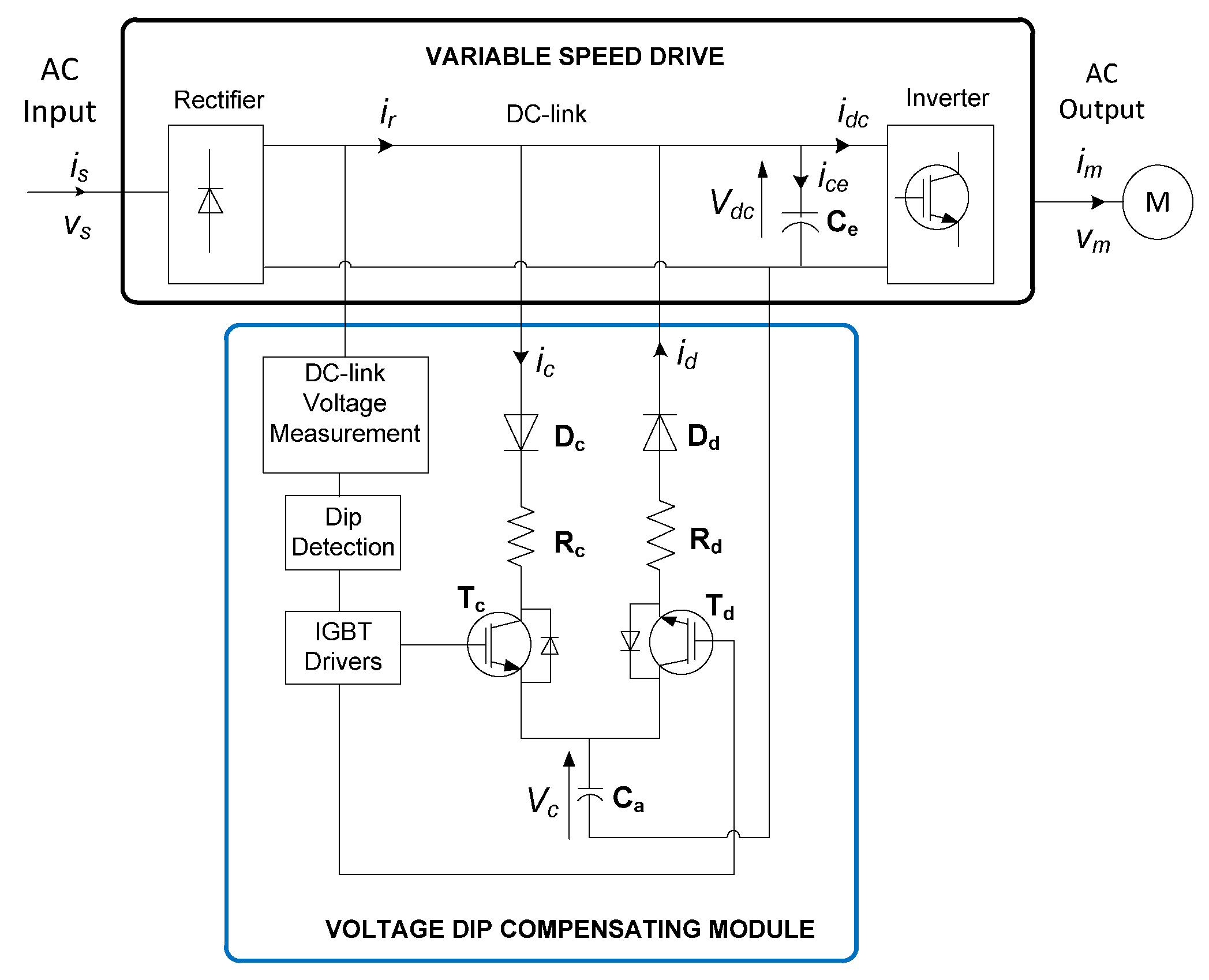
Figure 1. Proposed voltage dip compensating module.
Energies 14 08257 g001
Figure 2. DC-link during compensation (discharge).
Energies 14 08257 g002
Figure 3. DC-link during charging.
Energies 14 08257 g003
Figure 4. Discharge inrush current limiting resistor sizing flow chart.
Energies 14 08257 g004
Figure 5. Switched capacitor sizing flowchart.
Energies 14 08257 g005
Figure 6. Charging inrush current limiting resistor sizing flowchart.
Energies 14 08257 g006
Figure 7. Simulation results without compensation of the dc-link, (a) supply and the dc bus voltage, (b) dc-link current and moto input current, (c) load torque and (d) motor speed.
Energies 14 08257 g007
Figure 8. Simulation results with dc-link voltage compensation, (a) dc-link and capacitor voltage, (b) Motor and capacitor discharge current (c) torque and (d) speed response.
Energies 14 08257 g008
Figure 9. Simulation results for dc-link charging of capacitor Ca, (a) supply voltage, dc-link and (b) capacitor voltage, (c) capacitor charging current and (d) motor input current.
Energies 14 08257 g009
Figure 10. Block diagram of experimental set-up.
Energies 14 08257 g010
Figure 11. Voltage dip generator.
Energies 14 08257 g011
Figure 12. Laboratory experimental set-up.
Energies 14 08257 g012
Figure 13. Experimental results without dc-link voltage compensation.
Energies 14 08257 g013
Figure 14. Experimental results with dc-link voltage compensation.
Energies 14 08257 g014
Figure 15. DC-link voltage variation during voltage compensation.
Energies 14 08257 g015
Figure 16. DC-link charging of capacitor Ca.
Energies 14 08257 g016
Table 1. Ride-through requirements.
Ride-through duration0.2 s
Voltage dipSTPI
Minimum acceptable dc-link voltage0.85 Vdc
Maximum permissible discharge current 14.1 A
Maximum permissible charging current 28.4 A
1 VSD (variable speed drive) maximum output current; 2 VSD inrush current.
Table 2. Key simulation results.
ParameterAt Start of Short Term Power Interruption(STPI)At End of Short Term Power Interruption (STPI)% Change 1
DC-link voltage 556 V471 V−15.3%
Capacitor voltage544 V500 V−8.1%
Speed916 rpm871 rpm−4.5%
Torque16.1 Nm15.8 Nm−1.9%
1 negative sign indicates a reduction in the measured parameter.
Table 3. DC-link and capacitor voltage variation during compensation of a 1.5 kW induction motor.
Parameterat Start of STPIat End of STPI% Change 1
DC-link voltage 556 V456 V−18.0%
Capacitor Voltage544 V488 V−10.3%
1 negative sign indicates a reduction in the measured parameter.
Table 4. Impact on speed and motor torque.
Parameterat Start of STPIat End of STPI% Change 1
Speed882 rpm860 rpm−2.5%
Torque15.7 Nm14.0 Nm−10.3%
1 negative sign indicates a reduction in the measured parameter.
Table 5. Comparison of key parameters.
ParameterChange in Value as Per *
Sizing MethodologySimulationExperiment
DC-link voltage drop15.0%15.6%18.0%
Cap voltage drop7.7%8.3%10.3%
* refers to change in value at the end of compensation compared to value at start of compensation.
Table 6. Capacitor charging and discharging currents.
ParameterValue Obtained as Per
Sizing MethodologySimulationExperiment
Discharge current (A)4.2 A4.2 A4.1 A
Charging current (A)8.4 A8.3 A9.5 A
Table 7. DC-link and capacitor voltage variation during compensation of a 7.5 kW induction motor.
ParameterValue Obtained as Per% Variance
Sizing MethodologySimulation
DC-link voltage drop83.4 V82.8 V0.7%
Cap voltage drop 54.0 V51.2 V5.3%
Table 8. Capacitor charging and discharging currents of a compensating module for 7.5 kw induction motor.
ParameterValue Obtained as Per% Variance
Sizing MethodologySimulation
Discharge current (A)27.89 A28.17 A1.0%
Charging current (A)20.88 A19.79 A5.4%
Publisher’s Note: MDPI stays neutral with regard to jurisdictional claims in published maps and institutional affiliations.