Article

Enhanced Boost Factor for Three-Level Quasi-Switched Boost T-Type Inverter

Faculty of Electrical and Electronics Engineering, Ho Chi Minh City University of Technology and Education, Ho Chi Minh City 700000, Vietnam
*
Author to whom correspondence should be addressed.
Energies 2021, 14(13), 3920; https://doi.org/10.3390/en14133920
Submission received: 27 May 2021 / Revised: 15 June 2021 / Accepted: 28 June 2021 / Published: 30 June 2021
(This article belongs to the Special Issue Power Electronic Converters: Control and Applications)

Abstract

:
A new modulation strategy has been introduced in this paper in order to enhance the boost factor for the three-level quasi-switched boost T-type inverter (3L-qSBT2I). Under this approach, the component rating of power devices is significantly decreased. Moreover, the use of a larger boost factor produces a smaller shoot-through current. This benefit leads to reducing the conduction loss significantly. Furthermore, the neutral voltage unbalance is also considered. The duty cycle of two active switches of a quasi-switched boost (qSB) network is redetermined based on actual capacitor voltages to recovery balance condition. Noted that the boost factor will not be affected by the proposed capacitor voltage balance strategy. The proposed method is taken into account to be compared with other previous studies. The operation principle and overall control strategy for this configuration are also detailed. The simulation and experiment are implemented with the help of PSIM software and laboratory prototype to demonstrate the accuracy of this strategy.

1. Introduction

Currently, a conventional three-level T-type inverter (3L-T2I) is applied for low voltage applications due to its advantages of low conduction loss due to not using extra diodes compared to neutral point clamped inverter (NPCI) configuration or producing better output quality compared to two-level inverter [1,2]. This topology is recently adopted for many applications, especially photovoltaic (PV) systems and motor drives, etc. [3,4,5]. Nevertheless, the traditional 3L-T2I produces a low value of AC output voltage in comparison to the input voltage of the inverter. Moreover, the conventional 3L-T2I cannot accept the shoot-through (ST) state during operation because of leading to a short circuit at the DC input source.
Nowadays, impedance-source inverters have been considered as a solution to deal with the drawbacks of conventional inverters [6,7,8]. By using some passive components such as diodes, capacitors, and inductors in Z-source (ZS) circuit, the ZS inverter (ZSI) can behave as a buck-boost inverter with ST immunity. During operation, the ST state is utilized to belong to traditional vectors of the inverter to enhance the output voltage. The result is that the reliability is significantly improved. According to these advantages, several applications based on ZSI were discussed for the motor drive system, micro-grid connection, and PV applications [9,10]. Many traditional multilevel inverter topologies were considered to incorporate with the ZS network, such as NPCI and 3L-T2I [11,12,13,14]. The works in [15,16] introduced a topology combining a single ZS network and 3L-T2I. To ensure a three-level voltage operation, this combination uses a split DC input source. The neutral point of this source is utilized to belong to of ZS circuit to feed to the three-level inverter circuit. This configuration must use one extra diode to guarantee the symmetry of the impedance network. Instead of using full-ST (FST) state, this method used upper-ST (UST) and lower-ST(LST) states to conform to the buck-boost characteristic, which is added within small vectors. In this strategy, the boost factor is equal to the traditional strategy in [8]. The work in [16] further proposed the neutral voltage balance strategy. However, this strategy required more dwell-time calculations and caused the boost factor effect.
To produce less component voltage rating and draw continuous input current, the quasi-Z-source (qZS) inverter (qZSI) has been presented in [17,18,19,20,21,22]. These topologies use the same components compared to ZSI, but these components were connected in another way. Like the ZS network, this type of impedance-source structure was considered to incorporate with the three-level inverter to provide multilevel characteristics [17,18,19,20,21,22]. In these approaches, two qZS circuits are connected to guarantee three-level operation at the output. However, the use of a large number of inductors and capacitors leads to increase volume and decrease power density of the inverter. Furthermore, buck-boost characteristics of the ZS/qZS inverters are only ensured by the ST duty ratio of the inverter branch, which decreases the flexibility of boost factor regulation. The literature [20] introduced the space-vector-modulation (SVM) method and the third harmonic injection scheme, which ensure the buck-boost operation by applying the UST and LST states. Similar to ZSI, these schemes required a split DC source to conduct UST and LST insertions. In [21,22], a novel SVM strategy was proposed to reduce the amplitude and the slew rate dv/dt of common-mode voltage (CMV). In this work, the neutral voltage unbalance problem was handled by adding one more extra small vector into the traditional switching sequence. However, the drew-time of additional small vectors is hardly determined. It produces the complexity of the calculation.
The quasi-switched boost (qSB) inverter (qSBI) was considered as an emerging topology that saves plenty of inductors and capacitors [23,24,25,26,27,28,29,30]. By installing one more active switch in the intermediate circuit, the boost factor of qSBI is so flexible to be controlled [16]. In this configuration, some advantages can be listed as high boost factor and voltage gain and good inductor current profile. These advantages lead to reducing voltage stresses on power devices and less capacitance requirement for passive components such as inductors and capacitors. The works of literature in [25,26,27,28,29,30] proposed the incorporation between qSB network and the multilevel inverter. In [25,26], the three-level NPCI was combined with two separated qSB networks. The 3L-T2I was considered to combine with this type of impedance-source network in [27,28,29,30]. In [27,28,29,30], the qSB network utilized only one inductor and one DC input source, which saves one inductor and a split DC source compared to [25]. These works also proposed a new pulse-width modulation (PWM) strategy based on the phase shift carrier method to provide some benefits such as high voltage gain [21,27], common-mode voltage elimination [28], the capability of operating in normal and open-circuit faults [29], and small component rating. Similar to other types of single-stage buck-boost inverter, this configuration also utilizes the FST state to obtain buck-boost voltage capability, which is inserted within a zero vector to not affect the other voltage vectors. The closed-loop control is employed for capacitor voltage balance, which requires a larger time interval for neutral voltage recovery. The work in [30] adopted a corresponding small vector to balance the neutral voltage. However, this way introduced more CMV amplitude, which is generated by small vectors.
In this paper, a new PWM method is introduced, which improves the boost factor as well as voltage gain of this configuration. The neutral voltage balance is also considered in this paper. Unlike the methods in [16,22,30], where the neutral-voltage balance is ensured by corresponding small vectors of the inverter side, the active switches of the impedance-source network are utilized to balance neutral voltage. The duty cycle difference of these switches is determined based on actual capacitor voltages. This method brings benefits of reducing balancing recovery time and calculation complexity compared to [16,22,27]. The duty cycle of these switches and modulation index are considered to adjust the output voltage of the impedance-source circuit and AC output voltage. The operation modes, as well as the mathematical analysis, will be presented in this paper. Some simulation and experiment setups are used to confirm the accuracy of the proposed modulation method. The rest of this paper consists of four sections as follows. Section 2 introduces the operation of the inverter and proposed PWM strategy. Section 3 presents a neutral voltage balancing scheme. In Section 4, a comparison study has been conducted to highlight the contribution of this scheme. In Section 5, the simulation and experimental results have been presented to confirm the accuracy of the introduced method. Section 6 presents a conclusion.

2. Proposed PWM Scheme for 3L-qSBT2I

The 3L-qSBT2I is established by an impedance-source network and a 3L-T2I, as observed in Figure 1. The impedance-source network is constructed by two switches S1 and S2, four diodes D1, D2, D3, and D4, two capacitors C1 and C2, and one inductor LB. The outputs of the intermediate circuit are “P”, “O”, and “N”, which are used to ensure the three-level operation of the inverter. The three-phase resistive load is adopted to confirm the operation of the inverter with the proposed scheme, which is fed through a three-phase LC filter to guarantee the sinusoidal waveform of output load voltage with a low THD value, as depicted in Figure 1. The control scheme of this configuration is detailed in the rest of this section. The operating modes, steady-state analysis, and parameter selection are also presented.

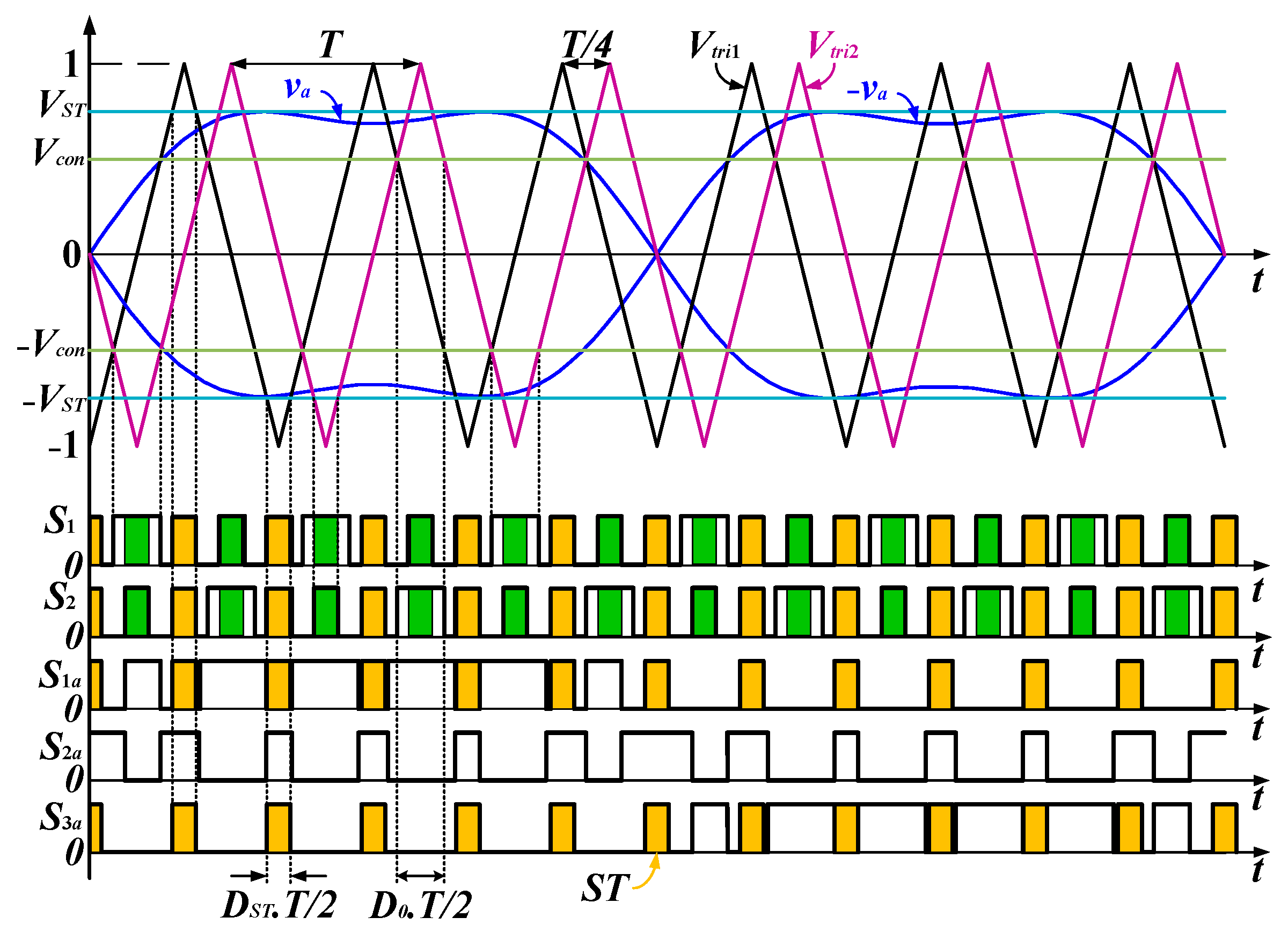
2.1. PWM Signal Generation

The control method for the 3L-qSBT2I is based on a phase-shift sinusoidal PWM scheme. The PWM control signal generation is divided into two cases: (1) inverter side PWM generation and (2) impedance-source switch PWM generation. For the inverter side, the six reference sinusoidal signals (±va, ±vb, and ±vc) are compared with a high-frequency triangle signal (Vtri1) to generate control signals for the inverter switches. Figure 2 shows the control signal generation for switches of phase A. In detail, switch S1A is turned on when −va < Vtri1 < +va, switch S3A is triggered on when +va < Vtri1 < −va, and switch S2A is turned on when switches S1A and S3A are off. Signals VST and −VST are used to create the ST signal denoted by yellow highlight in Figure 2. This ST state is generated by turned on all switches on the inverter side. In order not to affect the output voltage, the VST must not be smaller than the peak value of reference signals.
For the impedance source side, the triangle signal (Vtri2) is used, which is shifted 90 degrees compared to Vtri1 to create the control signals for the active switches of the impedance-source network [27]. Signals VST and −VST are also used with Vtri2 to generate the ST signal of the intermediate network, which is denoted by green highlight, as shown in Figure 2. Furthermore, two control signals, Vcon1 and Vcon2, are further used to enhance the duty ratio of S1 and S2, as illustrated in Figure 2.

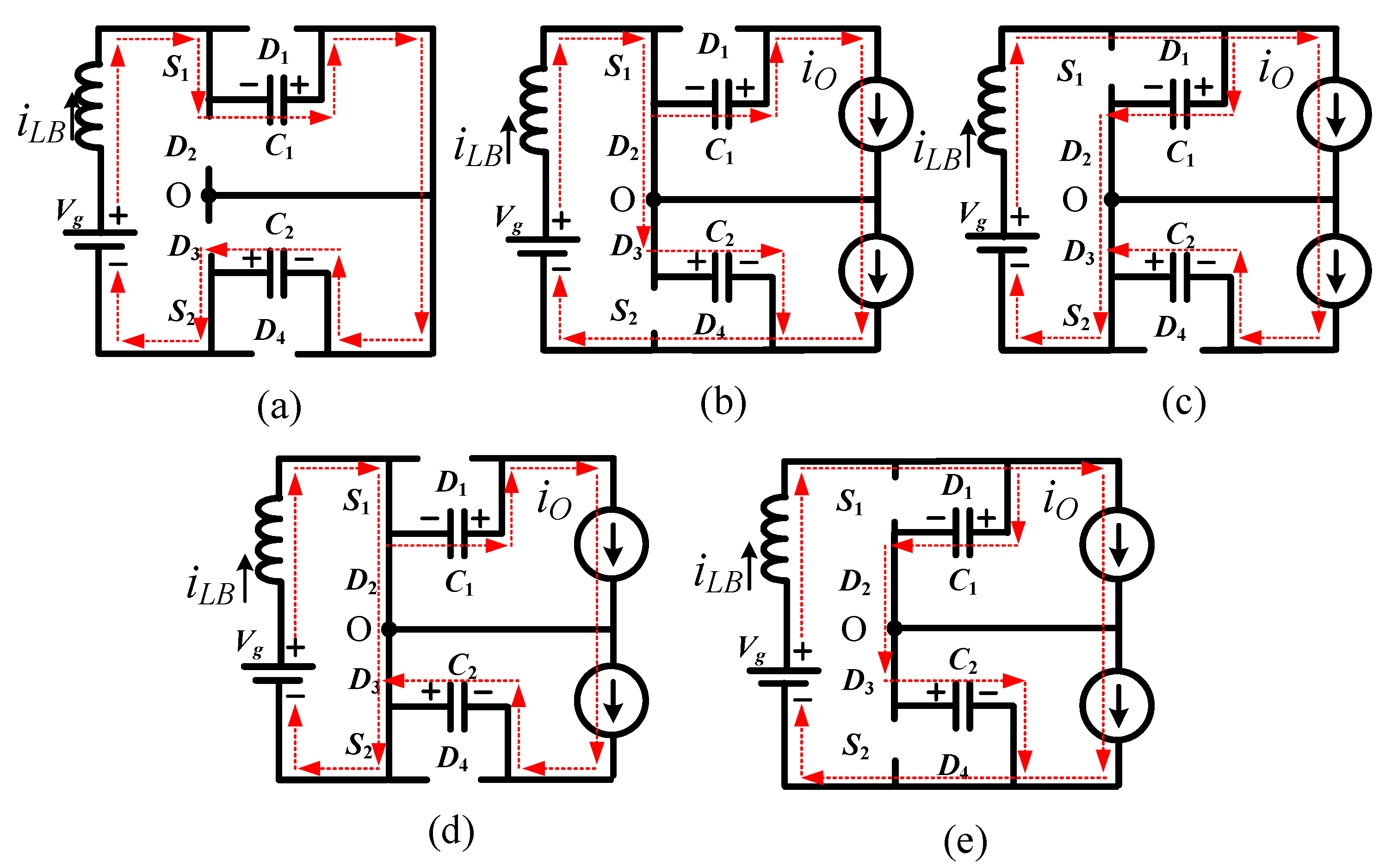
2.2. Operating Modes

Based on the PWM strategy presented in Figure 2, the inverter can be operated under two modes which are ST and non-ST (NST) modes. These modes are divided into five modes, which are ST mode, NST mode 1, NST mode 2, NST mode 3, and NST mode 4, as observed in Figure 3. To simplify, in non-ST modes, the inverter side is considered a current source, iO. The on switches and forwarded diodes are shown in Table 1.
In ST mode, both switches S1 and S2 of the qSB circuit and all switches of inverter side are turned on at the same time. The result is that input inductor LB is stored energy from the input source and C1 and C2 capacitors, as shown in Figure 3a. Conversely, methods in [27,30] only turned on all switches of inverter side, which decrease energy stored in the inductor and boost factor. The voltage across inductor LB and current across two capacitors are expressed as
{ L B d i L B d t = V g + V C 1 + V C 2 C 1 d v C 1 d t = C 2 d v C 2 d t = i L B
In NST mode 1 and NST mode 2, as shown in Figure 3b,c, capacitors C1 and C2 are respectively charged from the DC input source and the energy of inductor LB. The following equations are obtained as
{ L B d i L B d t = V g V C 2 C 1 d v C 1 d t = i O ,   C 2 d v C 2 d t = i L B i O
{ L B d i L B d t = V g V C 1 C 1 d v C 1 d t = i L B i O ,   C 2 d v C 2 d t = i O
where iO is the equivalent output current.
In NST mode 3, as illustrated in Figure 3d, the inductor LB is stored energy from the DC input power supply, whereas two capacitors, C1 and C2, transfer energy to the load. The inductor voltage and capacitor currents are expressed as
{ L B d i L B d t = V g C 1 d v C 1 d t = C 2 d v C 2 d t = i O
NST mode 4 is shown in Figure 3e, the lower capacitor and upper capacitor are further stored energy in NST modes 1 and 2. In these modes, the voltage across the input inductor and capacitor currents are calculated as
{ L B d i L B d t = V g V C 1 V C 2 C 1 d v C 1 d t = C 2 d v C 2 d t = i L B i O

2.3. Steady-State Analysis

The key waveform of inductor current iLB and capacitor voltages VC1 and VC2 are depicted in Figure 4. Considering one switching period, the time intervals of ST state is DST.T. The time interval of NST mode 3 is also DST.T. The total time interval of NST mode 1 and NST mode 2 is (D0DST)T. The rest time of switching period is (1 − D0DST)T, which is the time interval of NST mode 4. The average values of inductor voltage ( V ¯ L B ) and capacitor currents ( I ¯ C 1 , I ¯ C 2 ) are calculated as in Equation (6). Noted that the following equations are achieved by considering VC1 = VC2.
{ V ¯ L = [ ( V g + 2 V C 1 ) D S T T + ( V g V C 1 ) ( D 0 D S T ) T + V g D S T T + ( V g 2 V C 1 ) ( 1 D 0 D S T ) T ] / T I ¯ C 1 = I ¯ C 2 = [ i L B D S T T i O ( D 0 D S T ) T / 2 + ( i L B i O ) ( D 0 D S T ) T / 2 i O D S T T + ( i L B i O ) ( 1 D 0 D S T ) T ] / T
In steady-state, these average values are equal to zero, thus the capacitor voltages and average value of inductor current can be expressed as:
{ V C 1 = V C 2 = V g 2 5 D S T D 0 I L B = 2 i O 1 D S T 2 5 D S T D 0
The max value of VPN voltage is identified by summing of two capacitor voltages and expressed as
V P N = V C 1 + V C 2 = 2 V g 2 5 D S T D 0
The boost factor is defined as
B = V P N V g = 2 2 5 D S T D 0
The first-order of output load voltage is identified as
V x , p e a k = 1.15 M V P N / 2 = 1.15 M V g 2 5 D S T D 0
The voltage gain, G, is calculated as
G = V x , p e a k V g / 2 = 2 · 1.15 M 2 5 D S T D 0
The relationship between two coefficients, DST and D0, is defined as
D S T D 0 1 D S T
From Equation (12), by adopting DST and 1 − DST for the coefficient D0, the minimum and maximum voltage gain is identified by the following equation, noting that the value (1 − M) is employed for DST
{ G min = 1.15 M / ( 3 M 2 ) G max = 2 · 1.15 M / ( 6 M 5 )

2.4. Parameter Selection

The inductor current ripple (∆iLB), illustrated in Figure 4, is calculated with the help of Equation (1) as
Δ i L B = 1 2 L B f s V g D S T ( 1 + 2 2 5 D S T D 0 )
where fs is the switching frequency.
Inductance, LB, is selected in term of ∆iLB/iLB ≤ %x as
L B μ 2 P O % x f s V g 2 D S T ( 1 + 2 2 5 D S T D 0 )
where %x, µ, and PO are the maximum percentage of inductor current ripple, the inverter efficiency, and the output power.
The peak-to-peak value of capacitor voltages, VC1 and VC2, illustrated in Figure 4, is calculated as
Δ v C 1 = Δ v C 2 = 1 2 C f s D 0 i O
The selection of capacitors, C1 and C2, is conducted in terms of ∆vC/VC ≤ %y as follows
C 1 = C 2 1 4 % y f s D 0 P O ( 2 5 D S T D 0 ) 2 μ V g 2 ( 1 D S T )
where %y is the maximum percentage of capacitor voltage ripple.
The voltage stresses of impedance switches and diodes are the same as capacitor voltage. The max currents of switches and diodes of the qSB circuit are equal to the max value of the current across the inductor (iLB,peak), which is calculated as
i L B , p e a k = μ P O V g + 1 4 L B f s V g D S T ( 1 + 2 2 5 D S T D 0 )
The current stresses of 3L-T2I switches are selected as
{ I S x y = i O , when 13 D S T + 3 D 0 4 I S x y = i L B / 3 , when 13 D S T + 3 D 0 > 4
where Sxy (x = 1, 2, 3; y = A, B, C) is the inverter side switch. The voltage across S1X and S3X is the same as the DC-link voltage, whereas it is half of the capacitor voltage for bidirectional switches.

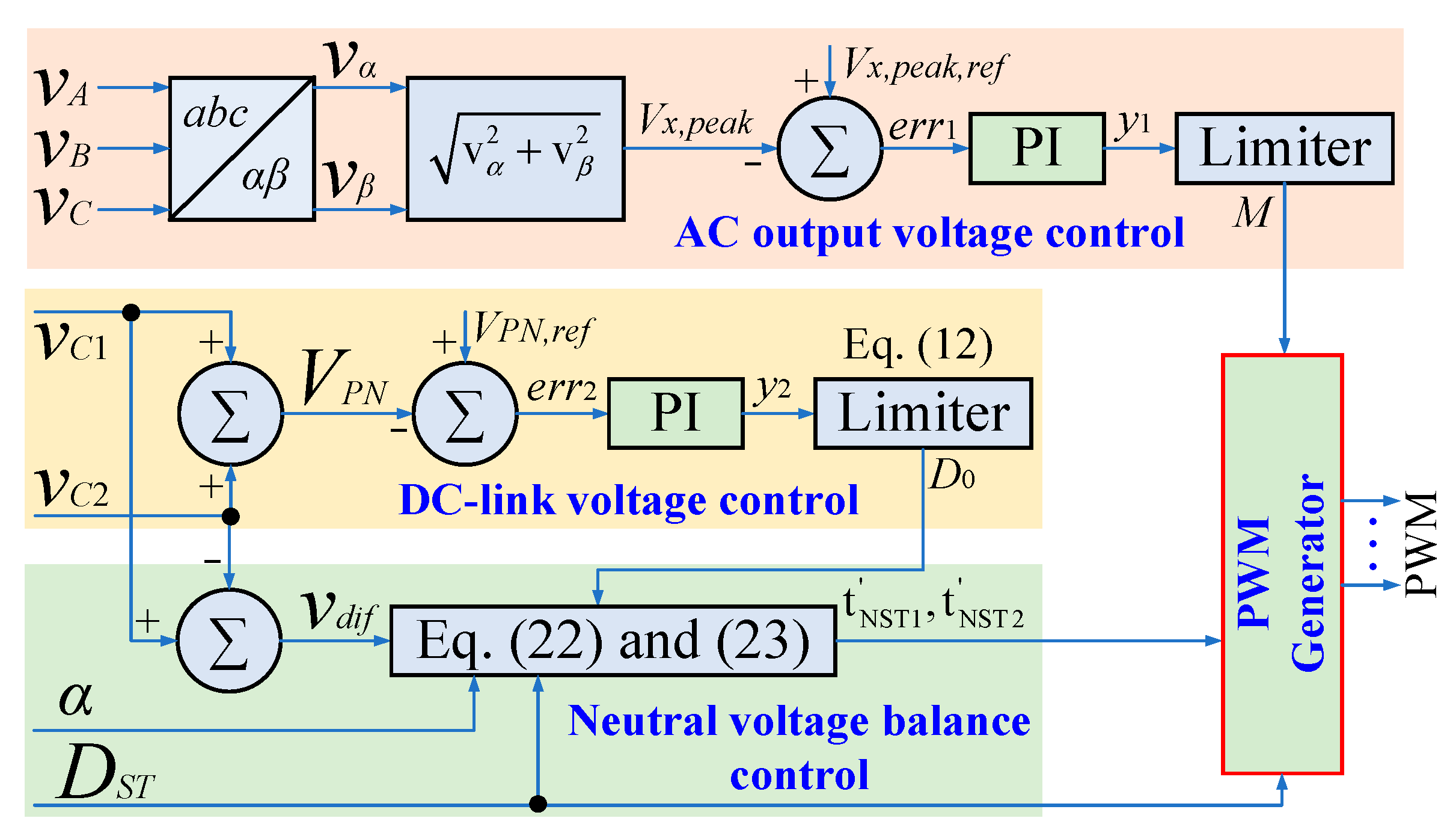
3. Proposed Capacitor Voltage Balance Scheme and DC-Link Voltage Control

As illustrated in Figure 3b, in NST mode 1, the capacitor C1 is discharged, whereas the capacitor C2 is stored energy from the input DC source and the input inductor LB. Therefore, in this mode, the voltage across C1 is reduced, while C2 voltage is raised. As opposed to NST mode 1, the C1 voltage is raised, while the C2 voltage is reduced, in NST mode 2, as illustrated in Figure 3c. Noted that these modes generate the same inductor voltage, VLB = VgVC, in terms of achieving a small difference between two capacitor voltages. Therefore, the boost factor is not much affected when replacing the NST mode 1 to NST mode 2, and vice versa.
To achieve a balancing condition, the proposed method replaces the NST mode 2 with NST mode 1 when VC1 > VC2. Conversely, NST mode 2 is utilized instead of NST mode 1 when VC2 > VC1, as presented in Figure 5. The S1 and S2 pulses are responsible for doing this work, which is detailed as follows. First, the traditional pulses of S1 and S2 are generated by using the Vtri2, ±VST, and ±Vcon, as shown in Figure 5. Then, VC1 and VC2 are considered to generate the final pulses of S1 and S2. Accordingly, the duty ratio of S2 is enhanced when VC1 > VC2. In contrast, the pulse of switch S1 is enhanced when VC2 > VC1.
In order to detail this strategy, the difference between the two capacitor voltages is defined as
v d i f = V C 1 V C 2
where:
vdif—the difference voltage between VC1 and VC2.
The total time offset, which is used to replace the NST mode 1 with NST mode 2 and vice versa, is identified as
Δ t = α t N S T 1 = α t N S T 2 = α ( D 0 D S T ) T / 2
where:
t—the time offset between NST mode 1 and NST mode 2 in one switching period;
tNST1 and tNST2—the traditional time intervals of the NST mode 1 and NST mode 2, respectively:
α—is the offset duty ratio (0 < α ≤ 1).
The capacitor voltage balance strategy is analyzed in two cases that depend on the sign of vdif.
In case 1, the sign of vdif is positive. To achieve capacitor voltage balance, in each switching period, the total time of the NST1 and NST2 can be redefined as
{ t N S T 1 = t N S T 1 + Δ t = ( 1 + α ) ( D 0 D S T ) T / 2 t N S T 2 = t N S T 2 Δ t = ( 1 α ) ( D 0 D S T ) T / 2
where t N S T 1 and t N S T 2 are the redefined time interval of NST mode 1 and NST mode 2 in one switching period.
In case 2, the sign of vdif is negative. To obtain capacitor voltage balance, in each switching period, the total time of NST mode 1 and NST mode 2 can be redefined as
{ t N S T 1 = t N S T 1 Δ t = ( 1 α ) ( D 0 D S T ) T / 2 t N S T 2 = t N S T 2 + Δ t = ( 1 + α ) ( D 0 D S T ) T / 2
Noted that the larger value of α leads to the faster neutral voltage balance speed. Moreover, having a fixed difference time ∆t between on-times of switches S1 and S2 makes this scheme easier to be employed than the method in [27]. As mentioned above, in this method, the operation of the inverter side is maintained, and the replacement of NST modes 1 and 2 produces the same voltage across the boost inductor. Therefore, this work does not affect the boost factor and voltage gain.
The control block diagram for the inverter is presented in Figure 6. In this figure, the controller consists of two separated parts, the DC-link voltage and AC output voltage regulations. From Equation (8), VPN can be regulated through two coefficients, DST and D0. Like [27], this scheme also fixes the value DST based on the DC source range. The result is that VPN is controlled through coefficient D0. Based on Equation (10), the AC output voltage control is achieved by adjusting capacitor voltage and modulation index M. However, when VPN regulation is obtained, the capacitor voltage is fixed at half of DC-link voltage VPN/2. Therefore, the AC voltage regulation is obtained by selecting the corresponding value of M.
For the DC-link voltage regulation, the actual value of VPN is obtained by totaling VC1 and VC2. The difference between VPN and the desired DC-link voltage, VPN,ref, is minimized by applying the PI controller. The coefficient D0 is reached by limiting the output of the PI controller by (12).
For the AC output voltage regulation, the actual output voltages (vA, vB, vC) are utilized to calculate the actual Vx,peak. The abc/αβ transformation is used to obtain this work, as shown in Figure 6. In this scenario, the PI controller is also considered to generate the modulation index M, noted that modulation index M is limited as (1 − DST).
After calculating three coefficients M, DST, and D0, the proposed scheme can generate the control signals of inverter switches similar to the conventional scheme. Noted that the time intervals of NST mode 1 and NST mode 2 have been adjusted, as mentioned above, to obtain neutral voltage balance.

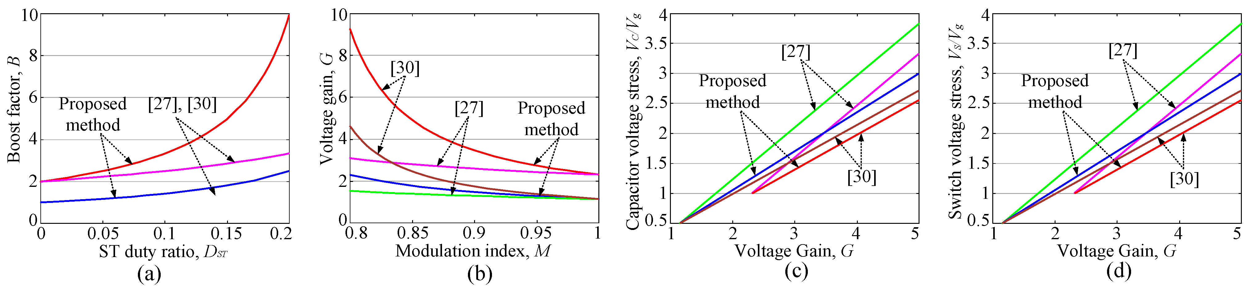
4. Comparative Study

In Section 4, the superior of the proposed method is demonstrated by comparing it to other single-stage inverters and schemes. The PWM strategies of 3L-qSBI in [27,30] are considered to make the comparison with the proposed method. The overview of boost factor, voltage gain, etc., comparison can be observed in Table 2 and Figure 7. In literature [27,30], the comparison between the qSBI, ZSI, and qZSI has been already conducted. It proved that the PWM method in [27,30] provides the highest boost factor and lowest component rating over other single-stage inverters. To simplify, only the PWM method in [27,30] is considered in comparison to the proposed method. It should be noted that the method in [27] is implemented with a third harmonic injection scheme instead of the sinusoidal scheme. This change increases the voltage gain of the method [27] to 1.15 times and does not affect the operation of the inverter. To achieve the highest performance, the DST is set to (1 − M) for the proposed method and the method in [27]. For the method in [30], the DST is set to 2(1 − M). In these methods, both the maximum boost and minimum boost schemes are investigated. The max boost control is achieved by setting D0 to (1 − DST), and the min boost control is obtained by applying DST to D0.
As shown in Figure 7a, when applying the same ST duty ratio, the boost factors, B, of the methods in [27,30] are the same, whereas the proposed method provides the largest boost factor. In voltage gain comparison, the proposed method and the method in [30] are the same, which is larger than that of the method in [27], for the same modulation index, M, as observed in Figure 7b. Due to having a larger boost factor, the proposed method needs a smaller DST than that of the methods in [27,30] for the same voltage gain. For example, when applying max boost control, if the proposed method needs the value k for DST to produce voltage G, the value of DST for the methods in [27,30] must be (1 + 2k)/(3k) and 2k, respectively. Noted that the most conduction loss of the single-stage inverter is mostly produced in ST mode, thus having smaller DST makes the proposed method produce less conduction loss than [27,30].
The capacitor voltage rating comparison is illustrated in Figure 7c. It proves that the proposed scheme has smaller voltage stress on the capacitor compared to the method in [27]. As mentioned in Section 4, the voltage stress on impedance-source switches and diodes are the same as capacitor voltage, while voltage stresses of upper and lower switches of inverter side S1X, S3X (X = A, B, C) are twice the capacitor voltage and that is half of the capacitor voltage for bidirectional switches. Therefore, the reduction of capacitor voltage stress causes a reduction of component rating of switches, as presented in Figure 7d.
In summary, the proposed method has produced the largest boost factor and voltage gain over other single-stage three-level buck-boost inverters such as ZSI and qSBIs. These advantages can cause capacitor voltage rating and semiconductor voltage rating reduction. Moreover, the largest boost factor can lead to reducing the conduction loss, which increases the overall efficiency of the inverter.

5. Simulation and Experimental Verifications

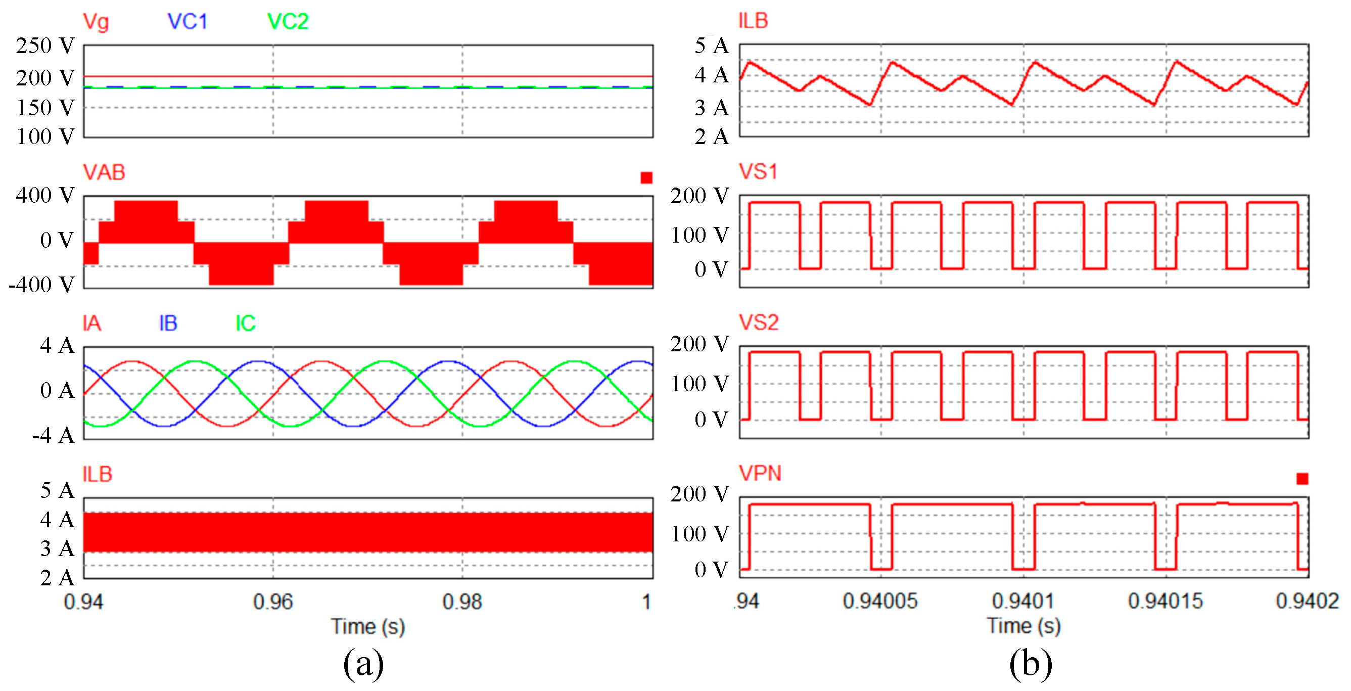
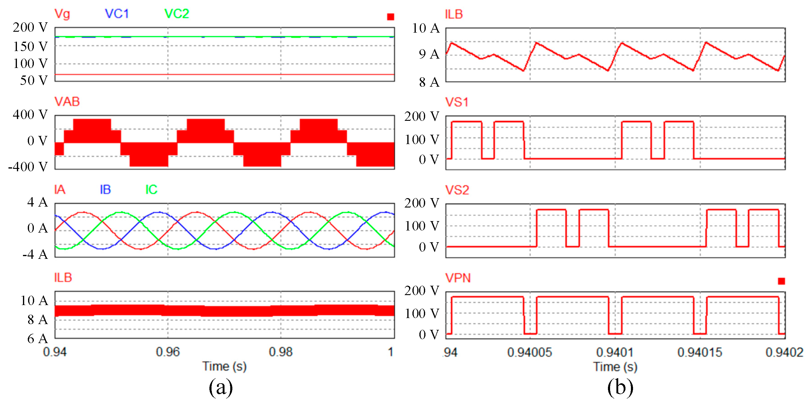
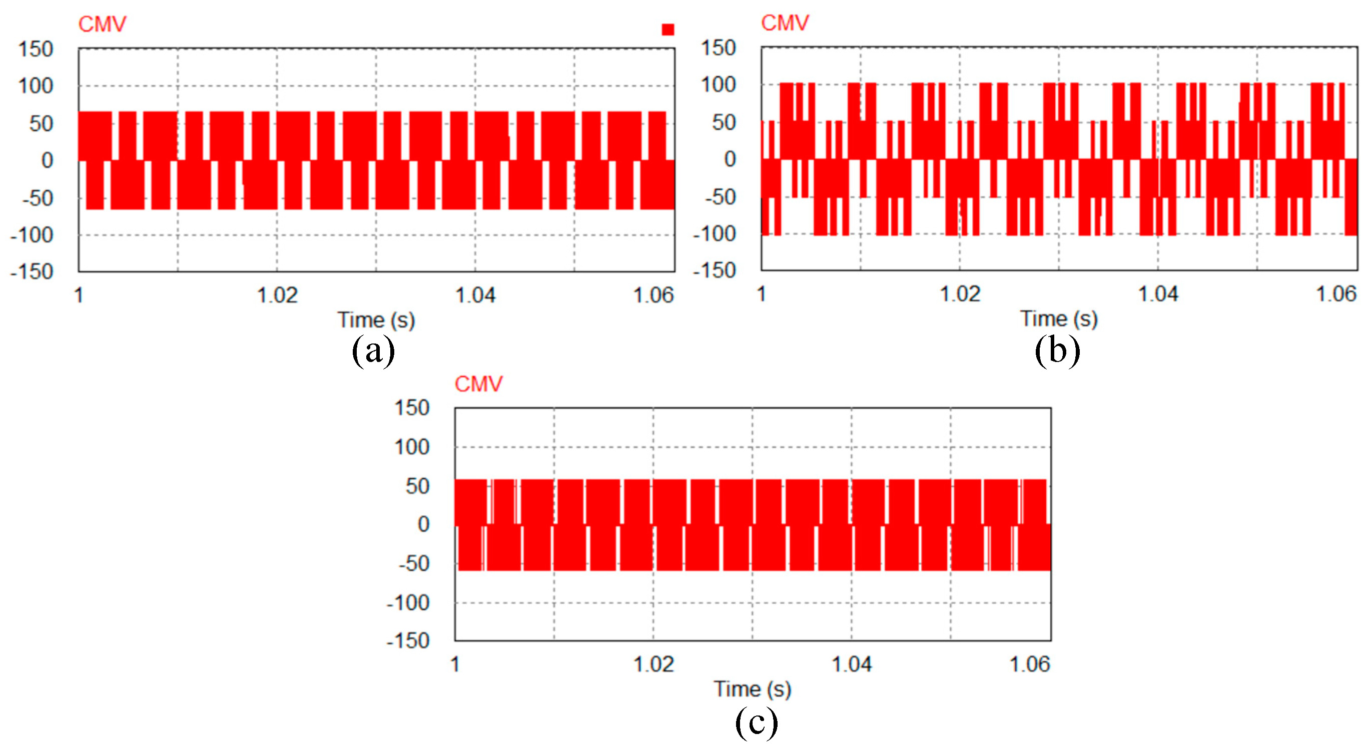
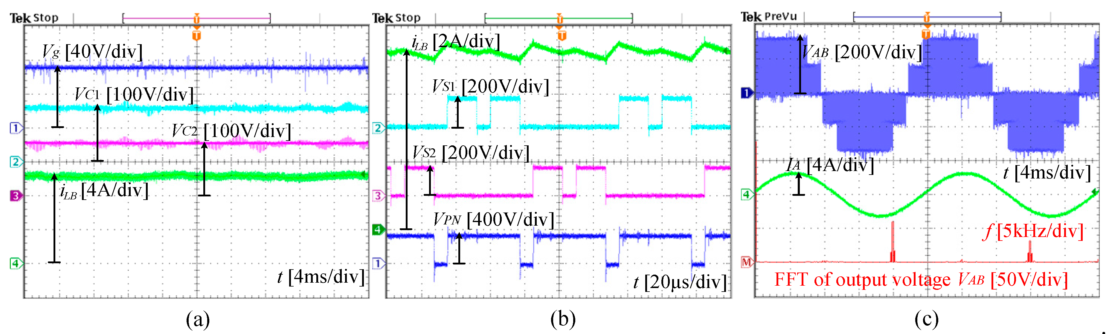
5.1. Simulation Results

With the help of PSIM simulation software, the simulation is conducted to validate the operation of the inverter under the proposed method. The simulation parameters are listed in Table 3. Both maximum and minimum boost factor control methods are validated with DC input range from 70 V to 200 V. In both cases, M and DST are set as 0.76 and 0.15, respectively. The extra duty ratio, D0, of switches S1 and S2 is set to 0.15 and 0.85 to achieve the min and max boost factors, respectively. With these control parameters, the AC output load voltage is maintained at 110 VRMS. The simulation results for both cases are shown in Figure 8 and Figure 9.
In both cases, the voltages on capacitors C1 and C2 are boosted to 180 V, as illustrated in Figure 8a and Figure 9a. These capacitor voltages are also the voltage stresses of switches S1 and S2, as shown in Figure 8b and Figure 9b. The peak value of VPN is 360 V, as illustrated in Figure 8b and Figure 9b. The maximum value inductor current ripple is approximately 1.5 A and 1 A for the cases of 200 V input voltage and 70 V input voltage, respectively. These values are obtained in ST mode, which is represented by the zero value of DC-link voltage, as presented in Figure 8b and Figure 9b. The inductor current, ILB, is also increased in NST 3, where S1 and S2 are turned on simultaneously. However, it is not increased faster than that of ST mode. The average inductor current is 3.4 A and 9 A for min boost and max boost control schemes, respectively. The waveform of VAB is varied from −360 V and 360 V, as shown in Figure 8a and Figure 9a. The THD value of VAB is 66%. The output load current is measured as 1.95 ARMS, and its THD value is 0.56% for both cases.
The comparison of CMV, VGO, between the proposed scheme and strategies in [27] and [30] is shown in Figure 10. The max boost control of methods in [27,30] is applied in the simulation. The method in [30] has the largest peak-to-peak CMV value of 200 V. It can be explained by using small vectors that generate a large value of CMV in [30]. The peak-to-peak CMV values of the scheme in [27] and the proposed PWM strategy are 130 V and 120 V, respectively. The RMS CMV values of the proposed method and methods in [27,30] are 34.8 VRMS, 36.5 VRMS, and 56.9 VRMS, respectively. It is proved that the proposed PWM strategy produces the smallest CMV.

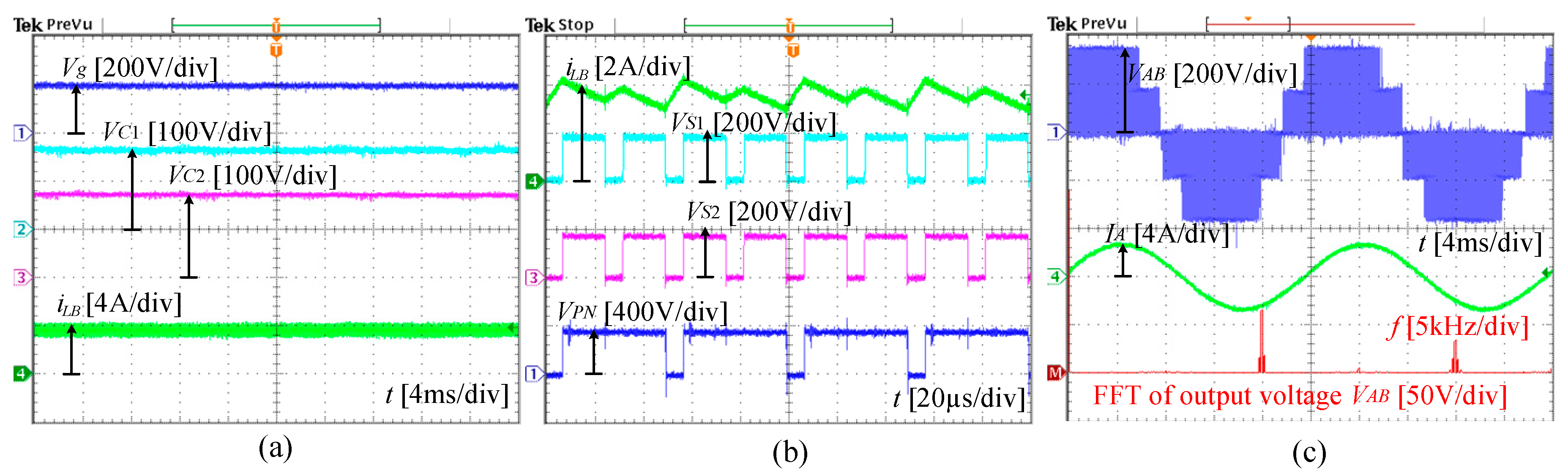
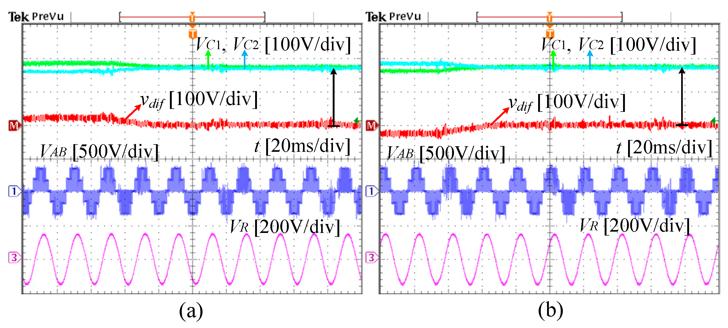
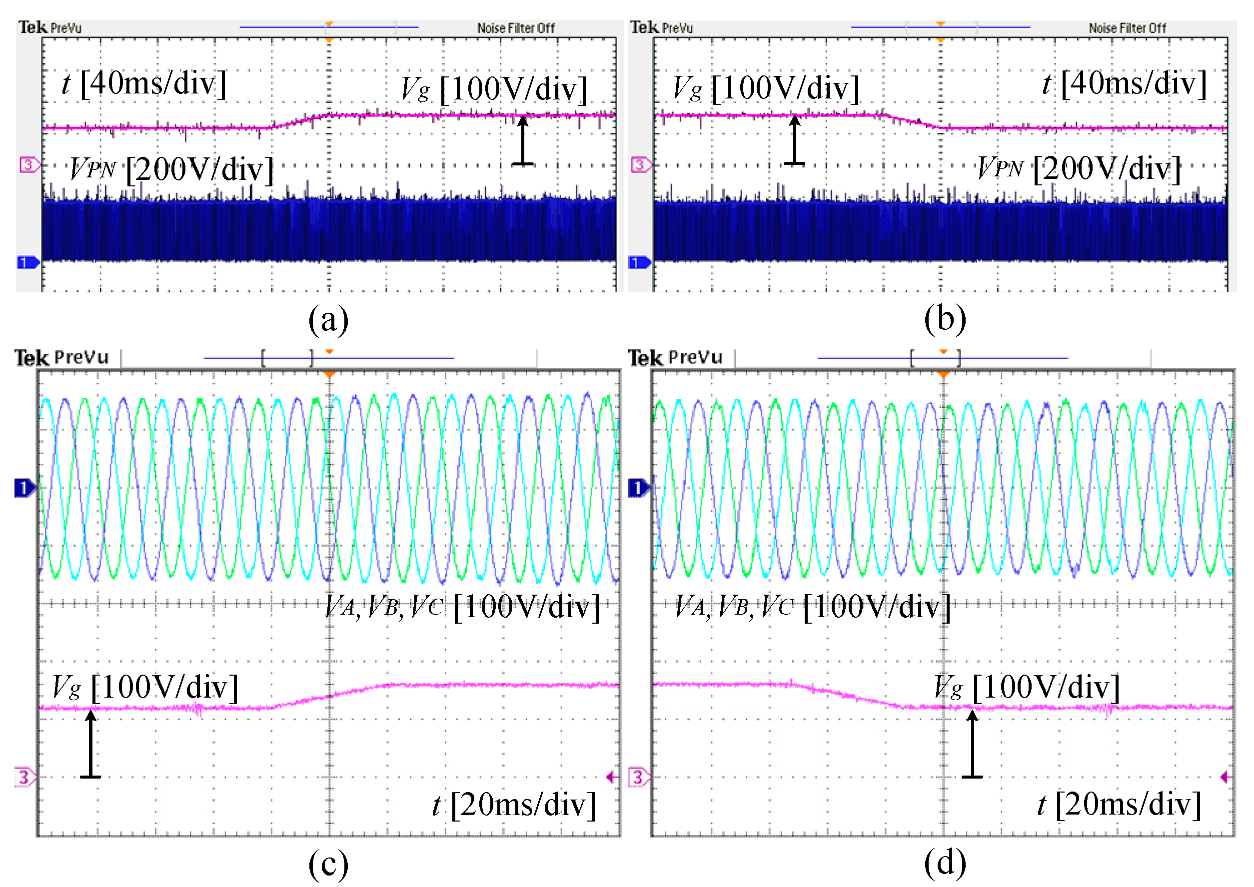
5.2. Experimental Results

The effectiveness of the proposed PWM strategy is also validated by experiments that are obtained through a laboratory prototype, as observed in Figure 11. The parameters used for experimental verification are also the same as simulation. The IGBTs FGL40N150 are used for the S1X and S3X of the inverter leg as well as the active switches of the intermediate network (S1 and S2). The isolated voltage sensors based on LEM LV20-P sensor are used to detect the capacitor and output load voltages. The experimental results are presented in Figure 12 and Figure 13.
For the case of a 200 V DC input source, as shown in Figure 12, the VC1 and VC2 are measured as 163 V and 170 V, respectively, as illustrated in Figure 12a. These capacitor voltages are also the voltage stresses of switches S1 and S2, which are 163 V and 170 V, respectively, as presented in Figure 12b. Furthermore, the max value of VPN is determined as 333 V, as shown in Figure 12b. The NST mode 3 can be determined by observing the value zero of both switch S1 and S2 voltages, while the ST mode can be identified by observing the value zero of DC-link voltage. The inductor current is increased in both NST mode 3 and ST mode, as shown in Figure 12b. However, in ST mode, the inductor current increment is faster than that of NST mode 3 because the voltage across the inductor is larger than that in NST mode 3, as demonstrated in Equations (1) and (4). Inductor current ripple is measured around 1.5 A. The average value of iLB is measured as 3.5 A, as presented in Figure 12a. The variation of VAB is from −VPN to +VPN, as illustrated in Figure 12c. The output load current is measured as 1.85 ARMS, and its waveform is sinusoidal. The FFT analysis for VAB can be seen in Figure 12c. The first-order harmonic is also the maximum value, which is 190 V. The THD values of VAB and output load current IA are 80.5% and 2.51%.
When applying 70 V DC input source, the capacitor C1 and C2 voltages are 153 V and 159 V, when the coefficient D0 is 0.85. These voltages generate 312 V of DC-link voltage, as illustrated in Figure 13b. The inductor current ripple is approximately 1.1 A, as shown in Figure 13b, and its average value is 10.4 A, as shown in Figure 13a. The output load current is 1.71 ARMS. Figure 13c presents the FFT spectrum of VAB, where the peak-to-peak value is 180 V at the first-order harmonic. The THD values of VAB and IA are 82.6% and 2.55%, respectively.
The capacitor voltage balance scheme and the closed-loop control implementation for the proposed method have been conducted. The results are shown in Figure 14 and Figure 15. The neutral voltage control is implemented in two cases: (1) the difference voltage between these capacitors vdif is positive, and (2) the difference voltage between these capacitors vdif is negative. In both cases, the neutral voltage balance condition is recovered after approximately 20 ms, as shown in Figure 14a,b. These results are conducted with the coefficient α of 0.3.
The input voltage is regulated to increase from 120 V to 160 V and decrease from 160 V to 120 V to validate the closed-loop control. In both cases, the VPN is maintained at 360 V, which can be seen from Figure 15a,b. The output load voltage is kept at 110 VRMS without DC input voltage variation, as presented in Figure 15c,d. In this work, the ST duty ratio DST is kept at 0.15. The modulation index is used to regulate the output load voltage and is limited to 0.85. The coefficient D0 is utilized to control DC-link voltage, and its range is from 0.15 to 0.85.

6. Conclusions

This paper has introduced a PWM method for the 3L-qSBT2I based on a third harmonic injection scheme. By applying this method, many benefits have been obtained, such as high boost factor, high voltage gain, and less voltage rating on impedance-source network devices. These advantages have been validated through some investigations, which were conducted belonging to previous publications. The details of relevant equations and designed parameter selection have been presented. Furthermore, this paper also considered the capacitor voltage unbalance problem. The time interval of NST mode, which is generated by triggering only one switch of the qSB network, has been recalculated based on the actual capacitor voltages to provide neutral voltage balance characteristics. The output voltage and DC-link voltage have been controlled by using PI controllers. The extra duty cycle of two active switches of the qSB network was adopted to regulate DC-link voltage, whereas the modulation index has been utilized to regulate the AC output voltage. The accuracy of this scheme has been validated by simulation and experimental results. With some benefits listed, such as buck-boost operation, reduced conduction loss, the low voltage stress on devices, and an easy capacitor voltage balance scheme, the 3L-qSBT2I under the proposed method is suitable for PV applications where a low DC input voltage needs to be converted to a high AC output voltage with high efficiency and output quality.

Author Contributions

This article has received the same contributions from the authors. which include writing the paper and experiment implementation. This manuscript has been received agreement from all authors. This paper was a collaborative effort among all authors. D.-T.D., V.-T.T. and M.-K.N. conceived the methodology, conducted the performance tests and wrote the paper. All authors have read and agreed to the published version of the manuscript.

Funding

This research was funded by T2020-18TÐ project.

Institutional Review Board Statement

Not applicable.

Informed Consent Statement

Not applicable.

Data Availability Statement

This work was supported by the Advanced Power Electronics Laboratory, D405 at Ho Chi Minh City University of Technology and Education, Viet Nam.

Conflicts of Interest

The authors declare no conflict of interest.

References

  1. Zhang, Z.; Zhang, J.; Shao, S. A Novel Trapezoidal Wave Control Method for a Single-Phase Grid-Tied T-Type Inverter. IEEE Trans. Power Electron. 2021, 36, 4711–4722. [Google Scholar] [CrossRef]
  2. Wang, Z.; Wu, Y.; Mahmud, M.H.; Zhao, Z.; Zhao, Y.; Mantooth, H.A. Design and Implementation of a Highly Efficient Three-Level T-Type Converter for Low-Voltage Applications. IEEE J. Emerg. Sel. Top. Power Electron. 2020, 8, 578–588. [Google Scholar] [CrossRef]
  3. Nemade, R.V.; Pandit, J.K.; Aware, M.V. Reconfiguration of T-Type Inverter for Direct Torque Controlled Induction Motor Drives under Open-Switch Faults. IEEE Trans. Ind. Appl. 2017, 53, 2936–2947. [Google Scholar] [CrossRef]
  4. Li, X.; Xing, X.; Zhang, C.; Chen, A.; Qin, C.; Zhang, G. Simultaneous Common-Mode Resonance Circulating Current and Leakage Current Suppression for Transformerless Three-Level T-Type PV Inverter System. IEEE Trans. Ind. Electron. 2019, 66, 4457–4467. [Google Scholar] [CrossRef]
  5. Xing, X.; Zhang, C.; Chen, A.; Geng, H.; Qin, C. Deadbeat Control Strategy for Circulating Current Suppression in Multiparalleled Three-Level Inverters. IEEE Trans. Ind. Electron. 2018, 65, 6239–6249. [Google Scholar] [CrossRef]
  6. Roncero-Clemente, C.; Romero-Cadaval, E.; Ruiz-Cortés, M.; Husev, O. Carrier Level-Shifted Based Control Method for the PWM 3L-T-Type qZS Inverter with Capacitor Imbalance Compensation. IEEE Trans. Ind. Electron. 2018, 65, 8297–8306. [Google Scholar] [CrossRef]
  7. Ding, X.; Hao, Y.; Li, K.; Li, H.; Wei, Z.; Wu, W. Extensible Z-Source Inverter Architecture: Modular Construction and Analysis. IEEE Trans. Power Electron. 2021, 36, 1742–1763. [Google Scholar] [CrossRef]
  8. Peng, F.Z. Z-source inverter. IEEE Trans. Ind. Appl. 2003, 39, 504–510. [Google Scholar] [CrossRef]
  9. Mahmoudi, H.; Aleenejad, M.; Ahmadi, R. Modulated Model Predictive Control for a Z-Source-Based Permanent Magnet Synchronous Motor Drive System. IEEE Trans. Ind. Electron. 2018, 65, 8307–8319. [Google Scholar] [CrossRef]
  10. Singh, S.A.; Carli, G.; Azeez, N.A.; Williamson, S.S. Modeling, Design, Control, and Implementation of a Modified Z-Source Integrated PV/Grid/EV DC Charger/Inverter. IEEE Trans. Ind. Electron. 2018, 65, 5213–5220. [Google Scholar] [CrossRef]
  11. Birundha, S.; Saravanan, V. Design and development of Z source cascaded seven level inverter for solar photovoltaic system. In Proceedings of the 2015 International Conference on Computation of Power, Energy, Information and Communication (ICCPEIC), Melmaruvathur, Chennai, India, 22–23 April 2015; pp. 87–92. [Google Scholar]
  12. Loh, P.C.; Gao, F.; Blaabjerg, F.; Feng, S.Y.C.; Soon, K.N.J. Pulsewidth-Modulated Z-Source Neutral-Point-Clamped Inverter. IEEE Trans. Ind. Appl. 2007, 43, 1295–1308. [Google Scholar] [CrossRef]
  13. Loh, P.C.; Lim, S.W.; Gao, F.; Blaabjerg, F. Three-Level Z-Source Inverters Using a Single LC Impedance Network. IEEE Trans. Ind. Electron. 2007, 22, 706–711. [Google Scholar] [CrossRef]
  14. Annam, S.K.; Pongiannan, R.K.; Yadaiah, N. A Hysteresis Space Vector PWM for PV Tied Z-Source NPC-MLI with DC-Link Neutral Point Balancing. IEEE Access 2021, 9, 54420–54434. [Google Scholar] [CrossRef]
  15. Effah, F.B.; Wheeler, P.; Clare, J.; Watson, A. Space-Vector-Modulated Three-Level Inverters with a Single Z-Source Network. IEEE Trans. Ind. Electron. 2013, 28, 2806–2815. [Google Scholar] [CrossRef] [Green Version]
  16. Xing, X.; Zhang, C.; Chen, A.; He, J.; Wang, W.; Du, C. Space-Vector-Modulated Method for Boosting and Neutral Voltage Balancing in Z-Source Three-Level T-Type Inverter. IEEE Trans. Ind. Appl. 2016, 52, 1621–1631. [Google Scholar] [CrossRef]
  17. Stepenko, S.; Husev, O.; Vinnikov, D.; Fesenko, A.; Clemente, C.R.; Pimentel, S.P.; Santasheva, E. Experimental Comparison of Two-Level Full-SiC and Three-Level Si–SiC Quasi-Z-Source Inverters for PV Applications. Energies 2019, 12, 2509. [Google Scholar] [CrossRef] [Green Version]
  18. Stepenko, S.; Husev, O.; Vinnikov, D.; Fesenko, A.; Matiushkin, O. Feasibility Study of Interleaving Approach for Quasi-Z-Source Inverter. Electronics 2020, 9, 277. [Google Scholar] [CrossRef] [Green Version]
  19. Pires, V.F.; Cordeiro, A.; Foito, D.; Martins, J.F. Quasi-z-Source Inverter with a T-Type Converter in Normal and Failure Mode. IEEE Trans. Power Electron. 2016, 31, 7462–7470. [Google Scholar] [CrossRef]
  20. Wang, T.; Wang, X.; He, Y.; Chen, X.; Ruan, X.; Zhang, Z. An Improved Quasi-Z-Source Three-Level T-Type Inverter and Its Modulation Scheme. In Proceedings of the 2020 IEEE Applied Power Electronics Conference and Exposition (APEC), New Orleans, LA, USA, 15–19 March 2020; pp. 412–416. [Google Scholar]
  21. Qin, C.; Zhang, C.; Chen, A.; Xing, X.; Zhang, G. A Space Vector Modulation Scheme of the Quasi-Z-Source Three-Level T-Type Inverter for Common-Mode Voltage Reduction. IEEE Trans. Ind. Electron. 2018, 65, 8340–8350. [Google Scholar] [CrossRef]
  22. Qin, C.; Zhang, C.; Xing, X.; Li, X.; Chen, A.; Zhang, G. Simultaneous Common-Mode Voltage Reduction and Neutral-Point Voltage Balance Scheme for the Quasi-Z-Source Three-Level T-Type Inverter. IEEE Trans. Ind. Electron. 2020, 67, 1956–1967. [Google Scholar] [CrossRef]
  23. Nguyen, M.K.; Lim, Y.C.; Park, S.J. A Comparison between Single-Phase Quasi- Z-Source and Quasi-Switched Boost Inverters. IEEE Trans. Ind. Electron. 2015, 62, 6336–6344. [Google Scholar] [CrossRef]
  24. Tran, V.T.; Do, D.T.; Do, V.D.; Nguyen, M.K. A Three-Level DC-Link Quasi-Switch Boost T-Type Inverter with Voltage Stress Reduction. Energies 2020, 13, 3727. [Google Scholar] [CrossRef]
  25. Sahoo, M.; Keerthipati, S. A Three-Level LC-Switching-Based Voltage Boost NPC Inverter. IEEE Trans. Ind. Electron. 2017, 64, 2876–2883. [Google Scholar] [CrossRef]
  26. Sahoo, M.; Kumar, S. A single source fed three level voltage boost NPC inverter with reduced LC count. In Proceedings of the IECON 2016-42nd Annual Conference of the IEEE Industrial Electronics Society, Florence, Italy, 23–26 October 2016; pp. 3190–3195. [Google Scholar]
  27. Do, D.T.; Nguyen, M.K. Three-Level Quasi-Switched Boost T-Type Inverter: Analysis, PWM Control, and Verification. IEEE Trans. Ind. Electron. 2018, 65, 8320–8329. [Google Scholar] [CrossRef]
  28. Do, D.T.; Nguyen, M.K.; Ngo, V.T.; Quach, T.H.; Tran, V.T. Common Mode Voltage Elimination for Quasi-Switch Boost T-Type Inverter Based on SVM Technique. Electronics 2020, 9, 76. [Google Scholar] [CrossRef] [Green Version]
  29. Do, D.T.; Nguyen, M.K.; Quach, T.H.; Tran, V.T.; Blaabjerg, F.; Vilathgamuwa, D.M. A PWM Scheme for a Fault-Tolerant Three-Level Quasi-Switched Boost T-Type Inverter. IEEE J. Emerg. Sel. Top. Power Electron. 2019, 8, 3029–3040. [Google Scholar] [CrossRef] [Green Version]
  30. Tran, V.T.; Nguyen, M.K.; Do, D.T.; Vinnikov, D. An SVM Scheme for Three-Level Quasi-Switched Boost T-Type Inverter with Enhance Voltage Gain and Capacitor Voltage Balance. IEEE Trans. Power Electron. 2021, in press. [Google Scholar] [CrossRef]
Figure 1. 3L-qSBT2I topology [27].
Energies 14 03920 g001
Figure 2. The proposed PWM scheme.
Energies 14 03920 g002
Figure 3. The modes of 3L-qSBT2I: (a) ST mode, (b) NST mode 1, (c) NST mode 2, (d) NST mode 3, and (e) NST mode 4.
Energies 14 03920 g003
Figure 4. The key waveform in switching period.
Energies 14 03920 g004
Figure 5. PWM generation for capacitor voltage balance.
Energies 14 03920 g005
Figure 6. Coordinate control between capacitor voltage balance and DC-link voltage regulation.
Energies 14 03920 g006
Figure 7. (a) The ST duty ratio vs boost factor, (b) modulation index vs voltage gain, (c) voltage gain vs capacitor voltage rating, and (d) voltage gain vs switch voltage rating.
Energies 14 03920 g007
Figure 8. The simulation results of the proposed method when Vg = 200 V. From top to bottom: (a) input voltage (Vg), capacitor voltage (VC1, VC2), line-to-line voltage (VAB), load current (IA, IB, IC), inductor current (ILB), (b) zoom in of inductor current (ILB), impedance switch voltages (VS1, VS2), DC-link voltage (VPN).
Energies 14 03920 g008
Figure 9. The simulation results of the proposed method when Vg = 70 V. From top to bottom: (a) input voltage (Vg), capacitor voltage (VC1, VC2), line-to-line voltage (VAB), load current (IA, IB, IC), inductor current (ILB), (b) zoom in of inductor current (ILB), impedance switch voltages (VS1, VS2), DC-link voltage (VPN).
Energies 14 03920 g009
Figure 10. CMV comparison between (a) the method in [27], (b) the method in [30], and (c) the proposed method.
Energies 14 03920 g010
Figure 11. Experimental prototype.
Energies 14 03920 g011
Figure 12. Experimental results of the inverter under the proposed method when Vg = 200 V. From the top to bottom: (a) Vg, VC1, VC2, and iLB; (b) iLB, VS1, VS2, and VPN; (c) VAB, IA, and FFT spectrum of the output voltage VAB.
Energies 14 03920 g012
Figure 13. Experimental results of the inverter under the proposed method when Vg = 70 V. From the top to bottom: (a) Vg, VC1, VC2, and iLB; (b) iLB, VS1, VS2, and VPN; (c) VAB, IA, and FFT spectrum of the output voltage VAB.
Energies 14 03920 g013
Figure 14. The experimental results for capacitor voltage balance. (a) vdif > 0, (b) vdif < 0.
Energies 14 03920 g014
Figure 15. The experimental verification for DC-link voltage control and output load voltage control. (a,c) Input voltage increment, (b,d) input voltage decrement.
Energies 14 03920 g015
Table 1. On/Off states of 3L-qSBT2I switches and diodes (X = A, B, C).
ModeON SwitchesON DiodesVXO
NST mode 1S1D2, D3, D4+VPN/2, 0 or −VPN/2
NST mode 2S2D1, D2, D3+VPN/2, 0 or −VPN/2
NST mode 3S1, S2D2, D3+VPN/2, 0 or −VPN/2
NST mode 4S1XD1, D2, D3, D4+VPN/2
S2X0
S3XVPN/2
ST modeS1, S2, S1X, S2X, S3X 0
Table 2. Overall comparison study of the proposed method and strategies in [27,30] for 3L-qSBT2I.
Strategy in [27]Strategy in [30]Proposed Method
Max ST duty ratio, DST1 − M2(1 − M)1 − M
Boost factor, B2/(3 − 2DSTD0)2/(3 − 2DSTD0)2/(3 − 5DSTD0)
Voltage gain, G1.15·MB1.15·MB1.15·MB
Capacitor voltage rating, Vc/Vdc1/(3 − 2DSTD0)1/(3 − 2DSTD0)1/(3 − 5DSTD0)
Diode voltage rating, VD/Vdc1/(3 − 2DSTD0)1/(3 − 2DSTD0)1/(3 − 5DSTD0)
Switch voltage rating, VS/Vdc1/(3 – 2DSTD0)1/(3 – 2DSTD0)1/(3 − 5DSTD0)
Table 3. Simulation and experiment parameters.
Parameter/ComponentsValues
Input voltageVg70 V ÷ 200 V
Output load voltageVx,RMS110 VRMS
Output frequencyfo50 Hz
Switching frequencyfs10 kHz
Extra duty ratioD00.15 ÷ 0.85
ST duty ratioDST0.15
Modulation indexM0.76
Boost inductorsLB3 mH/20 A
CapacitorsC1 = C22200 μF/400 V
LC filterLf and Cf3 mH and 10 μF
Resistor loadR56 Ω
Publisher’s Note: MDPI stays neutral with regard to jurisdictional claims in published maps and institutional affiliations.

