Article

Reliability Enhancement of Power IGBTs under Short-Circuit Fault Condition Using Short-Circuit Current Limiting-Based Technique

1
Electrical Engineering Department, K. N. Toosi University of Technology, Tehran P.O. Box 15875-4416, Iran
2
School of Electronics Engineering and Computer Science, Queen Mary University of London, London E1 4NS, UK
*
Author to whom correspondence should be addressed.
Energies 2021, 14(21), 7397; https://doi.org/10.3390/en14217397
Submission received: 16 August 2021 / Revised: 19 October 2021 / Accepted: 26 October 2021 / Published: 5 November 2021

Abstract

:
Like the widely-used semiconductor switch, Insulated Gate Bipolar Transistors (IGBTs) are subject to many failures and degradation in power electronic converters. In Short Circuit Fault (SCF), as the most reported failures in IGBTs, drastic, sudden temperature rise, and peak SCF current are widespread failures owing to a relatively long delay of the protection subsystem. This paper proposes a protection strategy to limit the junction temperature rise by limiting the SCF current by adding a small value resistor in the IGBT emitter. Second, it reduces the SCF current to a value much less than the saturated current. With the proposed control approach, sudden temperature rise during SCF is controlled, preventing significant failure in IGBTs. The extension of the permissible SCF time is achieved even for the cases with temporary arcs. A simple control loop activates in the SCF condition and does not create slow transients for the IGBT. The results of this paper are validated through simulation and experiment.

1. Introduction

Insulated Gate Bipolar Transistors (IGBTs) are one of the most important components in medium and high power converters. They are commonly used in traction systems [1,2], pulsed power supplies [3,4,5], HVDC circuit breakers [6,7,8], and solid-state transformers [9,10]. IGBTs and capacitors are the components with 34% failure rates in the power converters [11,12,13]. Short Circuit Faults (SCFs) are specially important as a frequent failure modes in the IGBT operation. There are several further factors that may break the device in particular cases; however, IGBT can withstand the SCF condition for a limited time, e.g., IGBTs can survive 10 μ s of SCF condition until it reaches thermal runaway [14,15]. Among serious failure modes during SCF condition, we can name latch-up [16], gate oscillation [17,18], self-turn off [19], thermal run away during the turn-off state [20,21], Negative Differential Resistance (NDR) [22,23], and Metal–Oxide–Semiconductor Field-Effect Transistor (MOSFET) mode [24]. Toward enhancing the reliability of IGBT devices, there have been several attempts in the literature.
The latch-up process occurs when the parasitic thyristor of the device is activated, and SCF current limiting of the IGBT malfunctions immediately. For latch-up, modifications in the structure of IGBTs are proposed in [25], which has been applied in newer generations of IGBTs. For the modern IGBTs, therefore, the advanced designs provide a homogeneously SCF current sharing between the device cells, and hence, less sensitivity to latch-up failure has been obtained. In the gate-oscillation, leading to gate-oxide breakdown, both gate circuit elements and structural factors play important roles, and specific design and implementation for gate-oscillations mitigation are required [26]. Structural modifications are also proposed for preventing self-turn-off and MOSFET modes [27]. In the NDR condition, the SCF current flows unevenly through the IGBT in the turning-off process, which results in the current filament. Therefore, structural parameters of IGBTs, such as temperature dependency of device bipolar current gain ( β P N P ) and the turning-off speed of the device, are the main origins of this mode [28]. The thermal runaway in the turn-off state is a major challenge for the low-power IGBTs. In this failure mode, the device can withstand the SCF until 50∼100 μ s after the SCF removal owing to the high leakage current. Considering the above discussion, limiting the SCF energy can be an effective approach for protecting the switch during this failure modes [20,29].
Besides the aforementioned, there are several efforts for protecting the IGBTs during SCF by shortening the SCF time interval with the general aim to minimize the SCF time and avoid the thermal runaway. In [30,31], de-saturation is proposed as an effective protection approach. In this technique, the collector-emitter voltage of the IGBT is monitored after the turn-on command to be negligible or not. In the SCF condition, this value is high and perceived as an indicator of device operation in its active region, and the IGBT must be turned off to terminate the SCF. The main drawback though is the mandatory blanking time (1∼5 μ s ) between sensing the fault and resolving it [32] due to some intrinsic differences, such as the gate threshold voltage ( V t h ), input capacitance ( C i s s ), and transconductance ( g f s ), resulting in different transient time intervals [31]. The second protection approach is based on the device current rate of change (di/dt) by sensing the Kelvin inductor voltage [33,34]. This approach has fast response in fault detection condition and is just suitable for the packages with visible Kelvin inductances. The third approach directly senses the collector current using shunts or current sensors [14,35]. In this approach, the observed current is filtered to avoid detection circuit malfunctioning subject to the noise and existing leakage inductance of the path, where the delay is unavoidable.
Overall, the existing protection strategies do not consider IGBTs failure modes during SCF condition and introduce delay. By limiting the SCF current, temporary SCF conditions like vacuum arcs can be omitted [6,7] in less than several μ s if the SCF current is accurately limited. The IGBT, however, must be turned off, and after fault removal and protection resetting, IGBT is turned on again for normal operation after a comparatively long period.
Using the SCF current limitation, this paper proposes a novel strategy for avoiding the failure modes under SCF conditions. When the SCF conditions occur, the IGBT peak current is restricted by a small value resistance. The SCF current amplitude is then controlled to a value much less than the maximum value reported in the IGBT datasheet. If the SCF is maintained for a longer period than is allowed, the IGBT is smoothly turned off. Our approach has the following advantages:
  • The junction temperature rise is much less than the case without current limiting.
  • The converter operation is not interrupted due to the temporary faults.
  • The IGBT failure modes in SCF relevant to the peak current can be more easily handled.
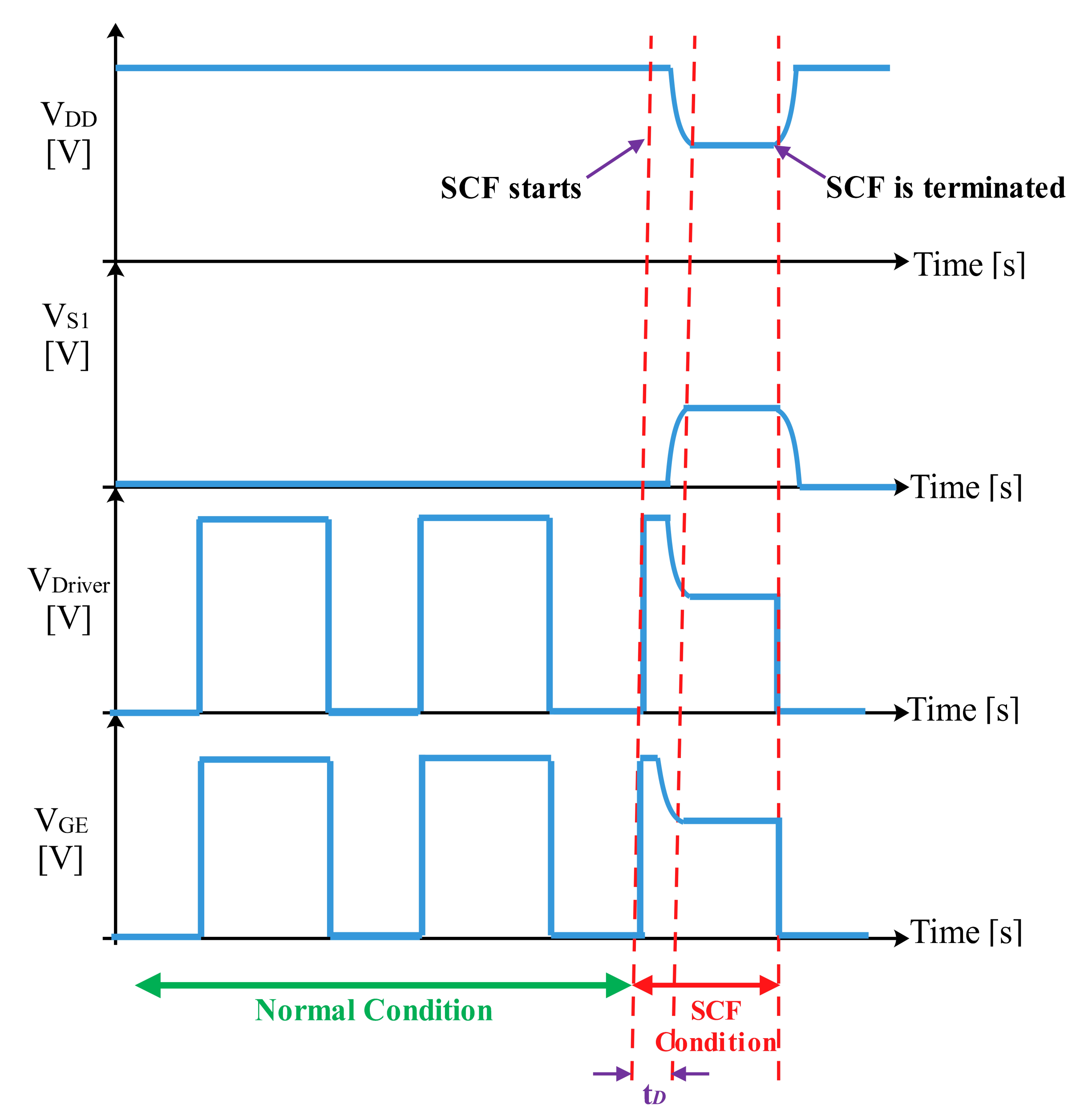
The first advantage is useful for the IGBTs with a small die where their junction temperature may considerably increase in SCF condition, and the failure in the turn-off state can be avoided by the proposed approach. The second advantage is applicable for mission-critical applications where the converter must be available seamlessly without any downtime for handling temporary faults. The third advantage can be used for all classes of IGBTs with different die structures and power ratings. The failure modes related to the IGBT SCF current, such as gate-oscillation, NDR, MOSFET mode, and self-turn off, can be easily managed. Our focus here is the temperature rise during the SCF, and the improvement in other failure modes is not the interest of this paper.
The rest of the paper is organized as follows: the proposed method is introduced in Section 2 where the operating principle, stability analysis, and improvements are described. The PSPICE simulations, finite element analysis are provided in Section 3, and finally, Section 4 provides the experimental results to validate the performance of the proposed method.

2. Proposed Method

We describe our proposed method in two phases: (1) the SCF peak current value of the IGBT is limited by a small value resistor in the device emitter connection, and (2) the limited SCF current is controlled by changing the gate-emitter voltage. When the method is applied, the short circuit (SC) energy is restricted, the SCF time interval is extended and a lower range drastic junction temperature rise is achieved. The following sub-sections describe the different phases:

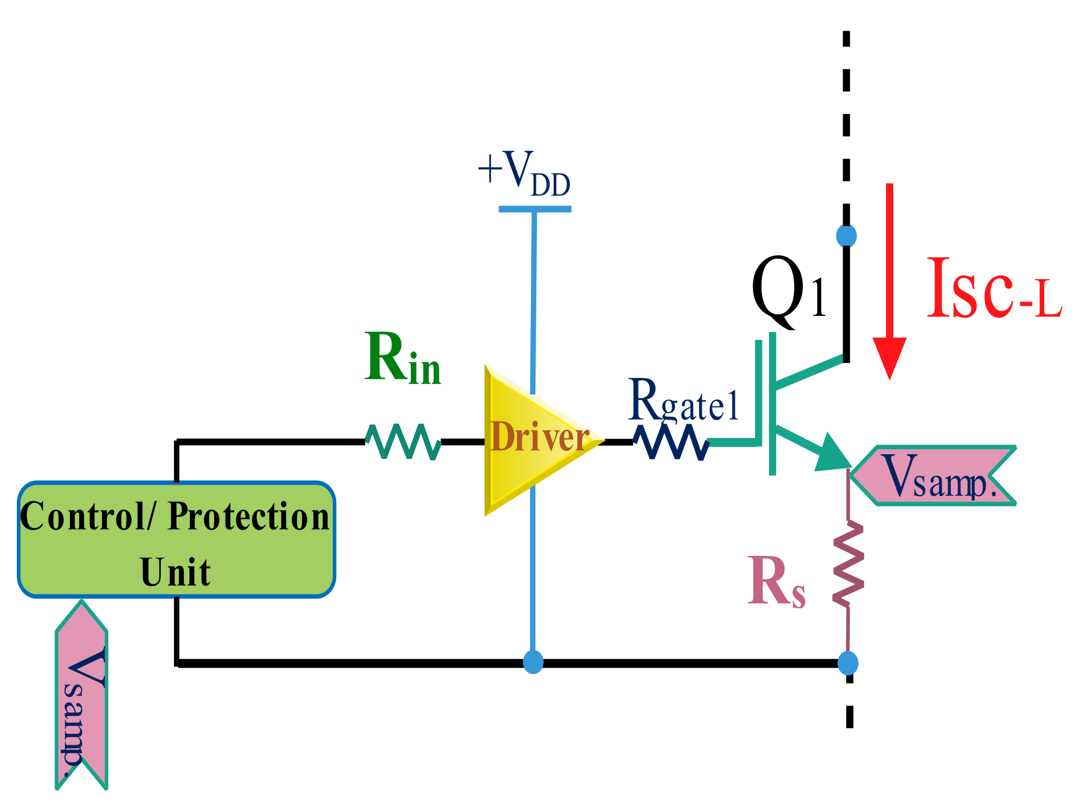
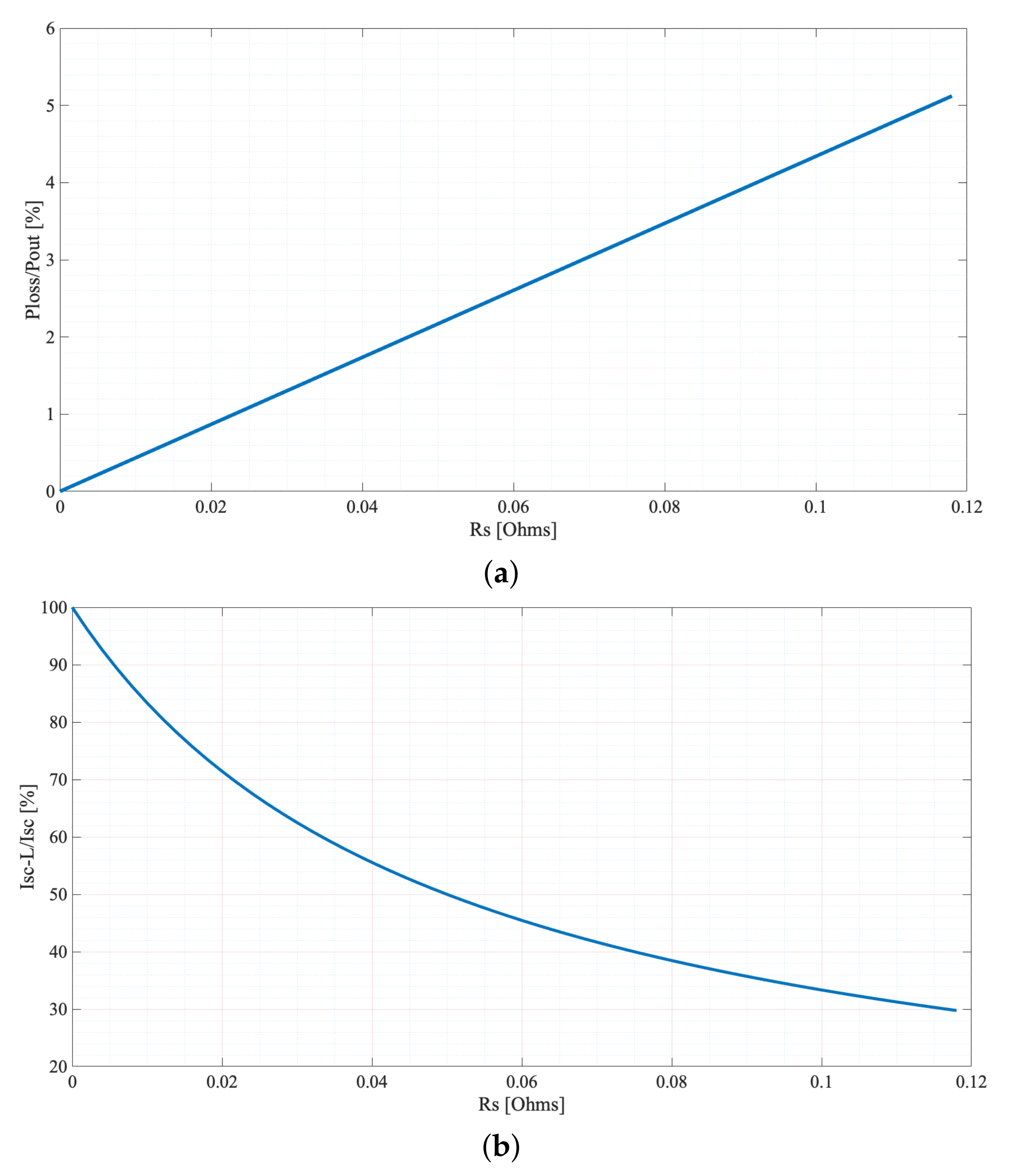
2.1. Limiting SCF Current

In this phase, we determine the maximum level of the SCF current by a small value resistance in the device emitter. The IGBT short-circuit current ( I S C ) is described as (1) [36].
I S C = ( 1 + β P N P ) μ n s C o x Z 2 L C H ( V G E V t h ) 2
where μ n s is the average electron mobility in the channel, C o x is oxide capacitance per unit area, Z is the channel width, L C H is the channel length, and V G E is the gate-emitter voltage level. I S C in (1) can be linearized as (2) using the method suggested in [15].
I S C = g f s ( V G E V t h )
g f s = I S C V G E = 1 1 α P N P μ n s C o x Z 2 L C H ( V G E V t h )
Insertion of a small value resistance at the IGBT emitter limits the short-circuit current ( I S C ) to limited short-circuit current named I S C L . According to (2) and Figure 1, the short-circuit current of IGBT ( I S C L ) is described as (4) and (5).
I S C L = g f s ( V D D V t h R S I S C L )
I S C L = g f s V D D V t h 1 + g f s R S
where V D D is the output voltage of the IGBT driver in the turn-on state, and R S is the resistance value of the resistor in the emitter of the device. Considering Equation (5), R S decreases the gate-emitter voltage of the IGBT in the SCF condition; hence, it can considerably decrease the IGBT saturated current. Note that the inclusion of R S in the proposed method is different from the well-known approach in which the fault current limiting resistor is directly placed in the power path. The value of R S in the proposed method is insignificant to effect the SCF current limiting without the IGBT. In fact, R S value is chosen such that it has negligible effect in the IGBT normal operation. However, the power loss of R S is not desired in high-power applications.
To clarify the effect of R S on the short circuit current limiting and the rising power loss, a case study is introduced (see Table 1). Figure 2 depicts the ratio of the limited SC current ( I S C L ) and SC current without applying R S ( I S C ), as well as the ratio of power loss of R S ( P l o s s ) and converter power ( P o u t ) as functions of R s . It is noteworthy to mention that P o u t is the converter output power value without R S . As expected, by increasing the value of R S the efficiency is slightly affected (see Figure 2a). Regarding Figure 2b, for R S values more than 0.05 Ω , the value of I S C L is considerably lower than I S C . As mentioned, to limit SCF current using R S is desirable for applications with low average power ratings, e.g., pulsed power supplies. However, in high or average power applications, the power loss is not insignificant; we need to apply the control method suggested in the second phase of our method, and described in Section 2.2.

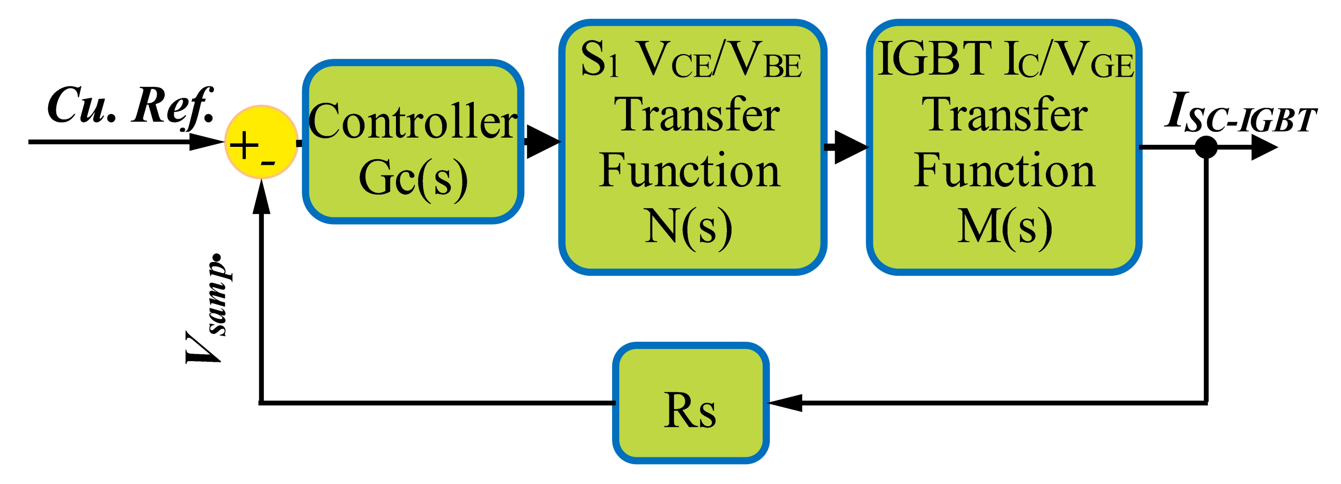
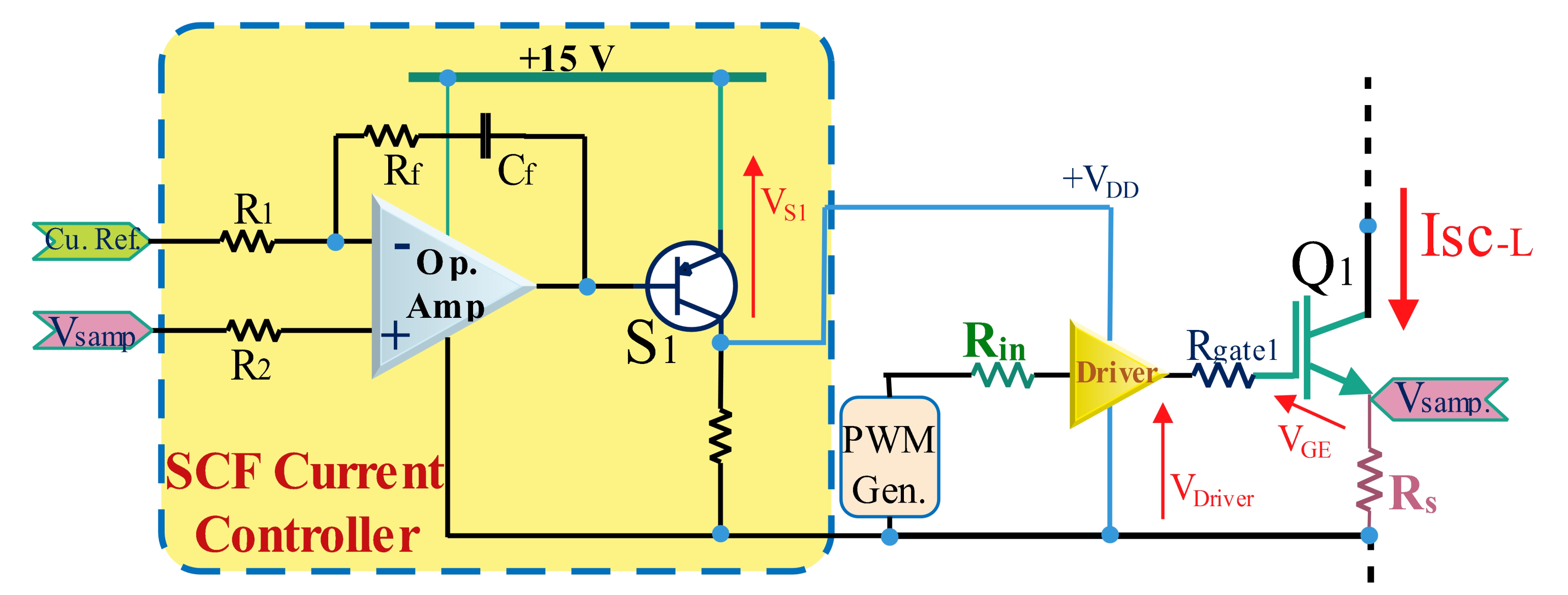
2.2. Controlling SCF Current

As pointed out, limiting the SCF current directly by R S is not practical for high and average power applications. Therefore, we propose a control method for SCF current which works based on controlling the gate-emitter voltage of the IGBT under SCFs (see Equation (2)). The method is described in Figure 3 where the control unit tunes the supply voltage level of the driver ( V D D ) to set the SCF current to a predetermined value.
The important signals of the proposed method in normal and SCF condition are provided in Figure 4. Accordingly, in the normal operation, the current reference (Cu. Ref. signal in Figure 3) is higher than IGBT current ( V s a m p signal in Figure 3). Therefore, the operational amplifier (OpAmp) sets the PNP transistor ( S 1 in Figure 3) to the turn-on state, and as a result, V D D reaches the maximum level, and the driver provides a +15 V voltage level for the IGBT gate-emitter. In the SCF condition, IGBT current exceeds the current reference. Meanwhile, the controller sets S 1 in the active region. Afterwards, voltage of S 1 increases, as depicted in Figure 4. Therefore, an appropriate value of the gate-emitter voltage is applied to the IGBT to control the SCF current. According to Figure 4, the proposed method is de-active in the normal condition. Thus, it does not negatively affect the IGBT transient times in turning-on/off processes which are seriously influenced by prior active gate control strategies [37,38].
However, the SCF current limiting unit reacts with some delays due to the limited bandwidth of the Op-Amp and S 1 . Therefore, in the delay interval, SCF current jumps to the limiting level determined by R S , and the control unit can now limit the SCF current (see the SCF current profile in Figure 5). In a hard SCF condition, where the IGBT enters to faulty condition abruptly from the normal condition, there is another current jump due to the resonance of the circuit inductance and the device capacitance elements. As described in [7], this current jump has a negligible energy and duration and can be ignored.

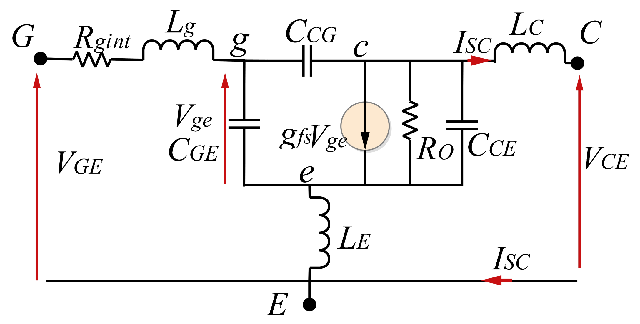
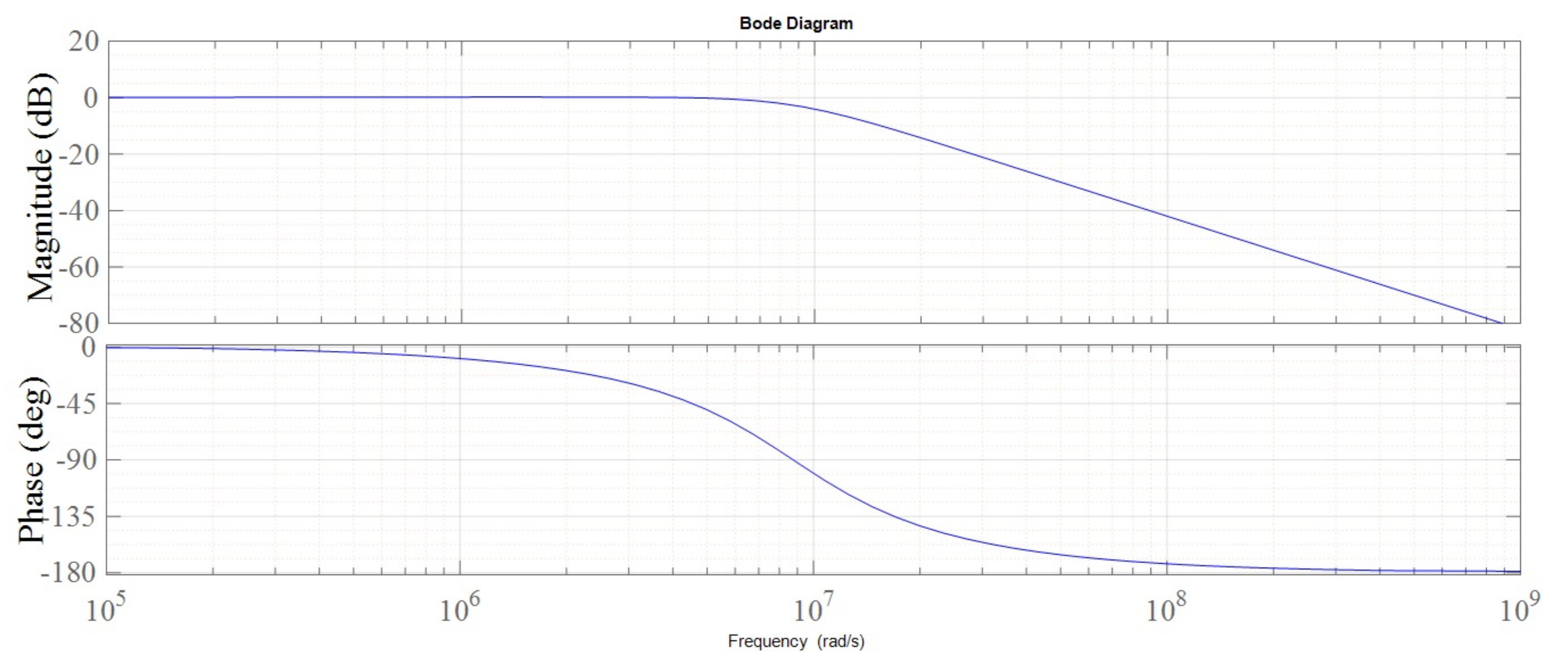
2.3. Stability Analysis

Our proposed method for controlling the SCF current is a closed-loop control and we need to ensure its stable steady-state operation (see the block diagram in Figure 6). Considering the IGBT model in Figure 7, the relation between the IGBT current ( I S C ) and the Gate-Emitter voltage ( V G E ) can be written as (6) [37]:
I S C ( s ) V G E ( s ) = a 3 s 3 + a 2 s 2 + a 1 s 1 + a 0 b 4 s 4 + b 3 s 3 + b 2 s 2 + b 1 s 1 + b 0
a 0 = g f s R O , a 1 = C C G R O , a 2 = L E ( C C E + C G E + g f s C G C R O ) , a 3 = L E R O ( C G C C G E + C G E C C E + C C G C C E ) , b 0 = R O , b 1 = L C + R G R O ( C G E + C G C ) + L E ( 1 + g f s R O ) , b 2 = R g i n t ( C G E + C G C ( 1 + g f s R O ) ) ( L C + L E ) + R O ( C G E ( L E + L g ) ) + C G C ( L C + L g ) + C C E ( L C + L E ) , b 3 = R O R g i n t ( C G C C G E + C G E C C E + C G C C C E ) ( L C + L E ) + ( L E L C + L g L E + L g L C ) ( C G E + C G C ( 1 + g f s R O ) ) , b 4 = R O ( L E L C + L g L E + L g L C ) ( C G C C G E + C G C C E + C G C C C E ) ,
where s is the complex frequency, and all the coefficients of (6) are defined in [37]. In addition, for the low-voltage and low-power PNP device ( S 1 ), the relation between the device collector-emitter ( V C E ) and base-emitter ( V B E ) can be written as (8).
V G E ( s ) V B E ( s ) = c 3 s 3 + c 2 s 2 + c 1 s 1 + c 0 d 3 s 3 + d 2 s 2 + d 1 s 1 + d 0
where the coefficients of (8) could be found in [38]. However, the S 1 transfer function has a wide-band frequency response since it is a low-power device. The controller transfer function is assumed to be a PI controller as defined in (9).
G C ( s ) = K p + K 1 s
Using MATLAB tools, the PI controller can be designed with the desired bandwidth and phase margin. The required parameters for determination of the coefficients in (6) are summarized in Table 2. For a 1 MHz bandwidth and a 60° phase margin, which equals to 300 ns settling time, the controller gain are designed as K p = 18 and K I = 4.1 × 10 6 . The closed-loop bode diagram of the SCF current controlling loop is shown in Figure 8, which approves that the controller is in the stable margin. The PI controller can be tuned by changing the values of R 1 , R 2 , R f , and C f in Figure 3.

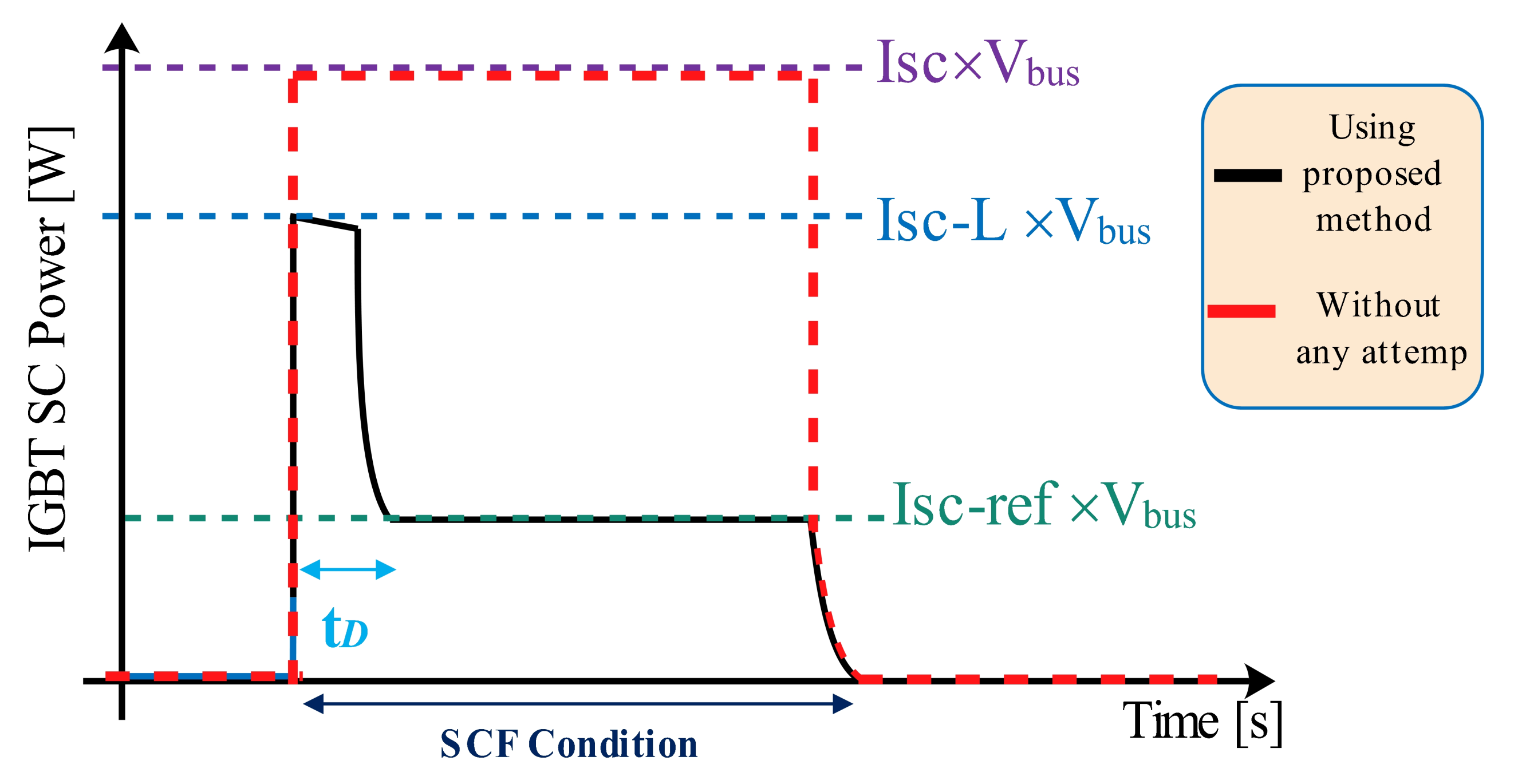
2.4. Short Circuit Energy

The main goal of the proposed method is to reduce short circuit energy during the SCF condition. Regarding the description of the proposed method, two intervals are specified during SCF condition:
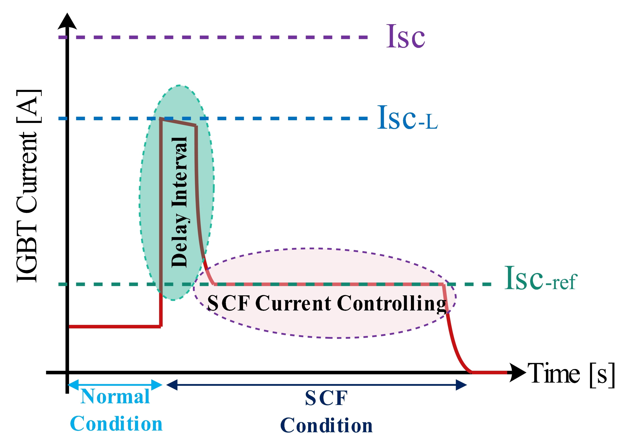
  • the first interval is called delay interval ( t D ), during which the SCF current is limited to I S C L ,
  • the second interval is the time duration in which the SCF current is controlled to the value of SCF current controller ( I S C r e f ).
As a result, the short circuit energy of the IGBT ( E S C ) is described as:
E S C = V b u s ( I S C L t D + I S C r e f ( t S C t D ) )
where t S C is the SCF time interval, and V b u s is the DC bus voltage applied to the device in SCF condition. t D strictly depends on the parasitic elements of the IGBT and the controller loop bandwidth, and is subject to small changes. However, I S C L , and I S C r e f can be determined in the design phase. The parameters R S , and Cu. Ref. are determined for particular limited and controlled SCF currents respectively. For the cases in which the risk of the temporary SCFs is high, the limited and controlled SCF currents are chosen to values near the load nominal current to extend the permissible SCF condition. In contrast, for the cases with high level of average power, the limited SCF current cannot be very low near the load nominal current due to the power (see Figure 2). Therefore, using the proposed method, SCF energy is decreased, which leads to a lower temperature rise and lower risk of failure due to the peak SCF current.

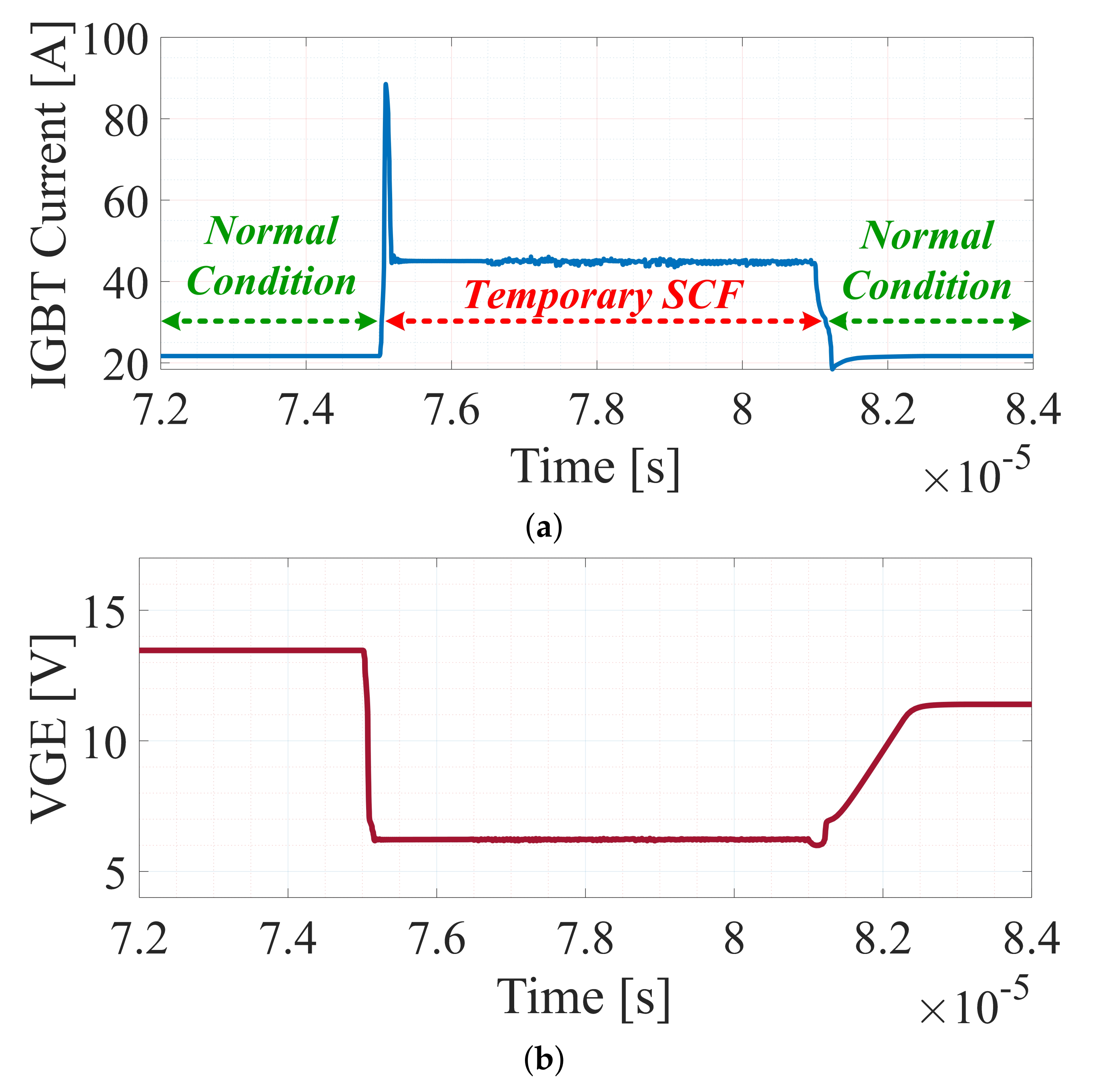
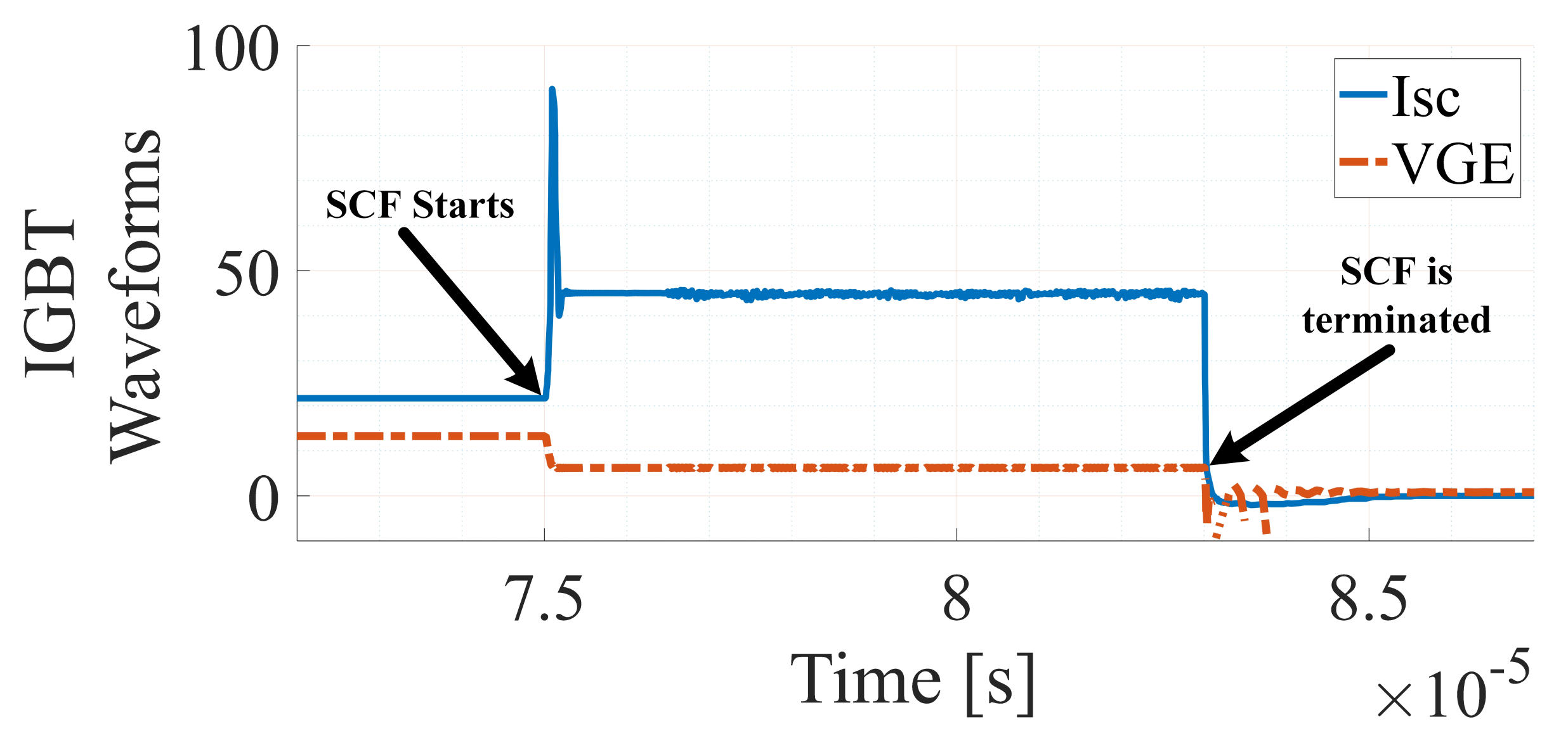
3. Simulation Results

3.1. PSPICE Simulation
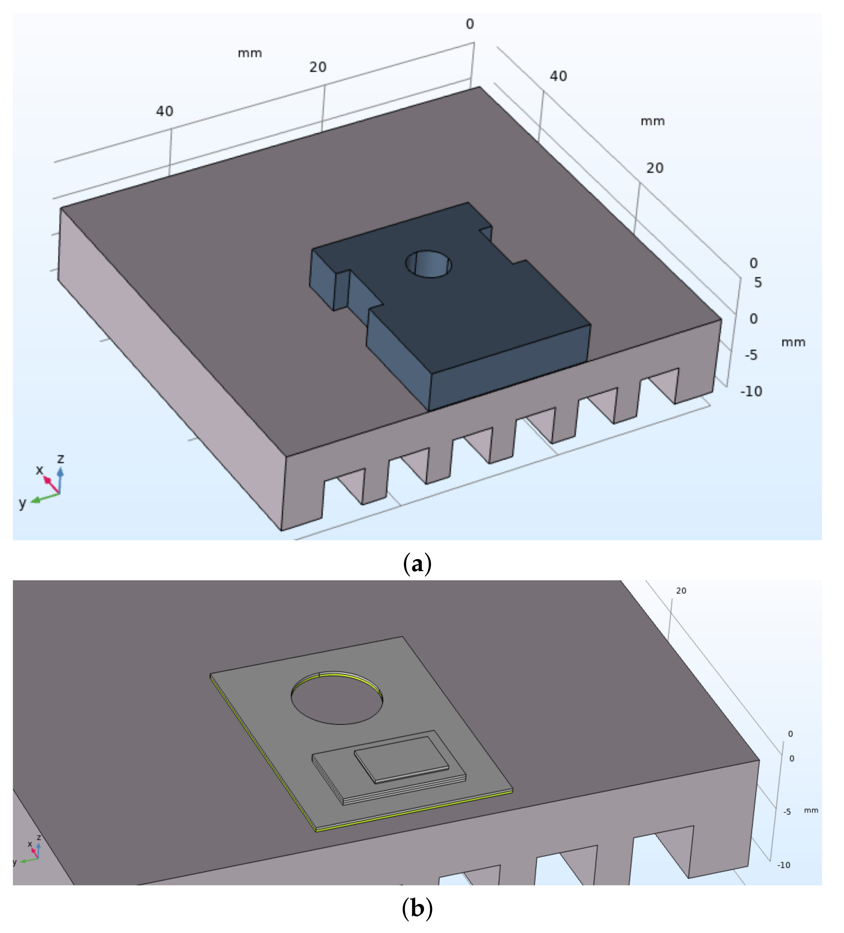
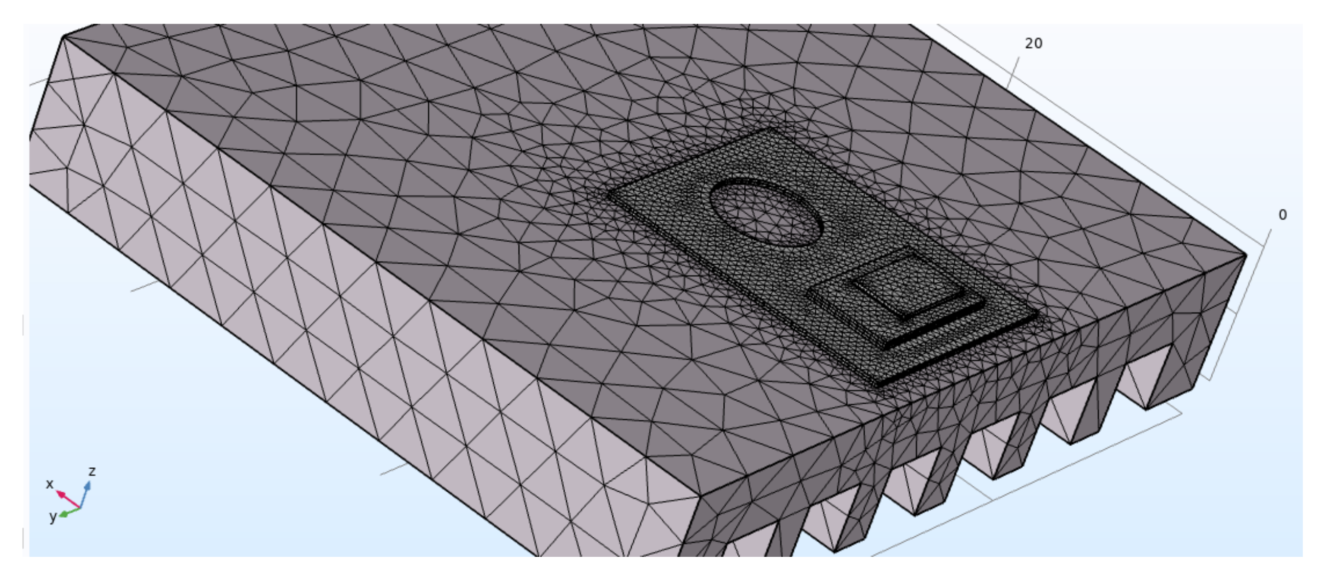
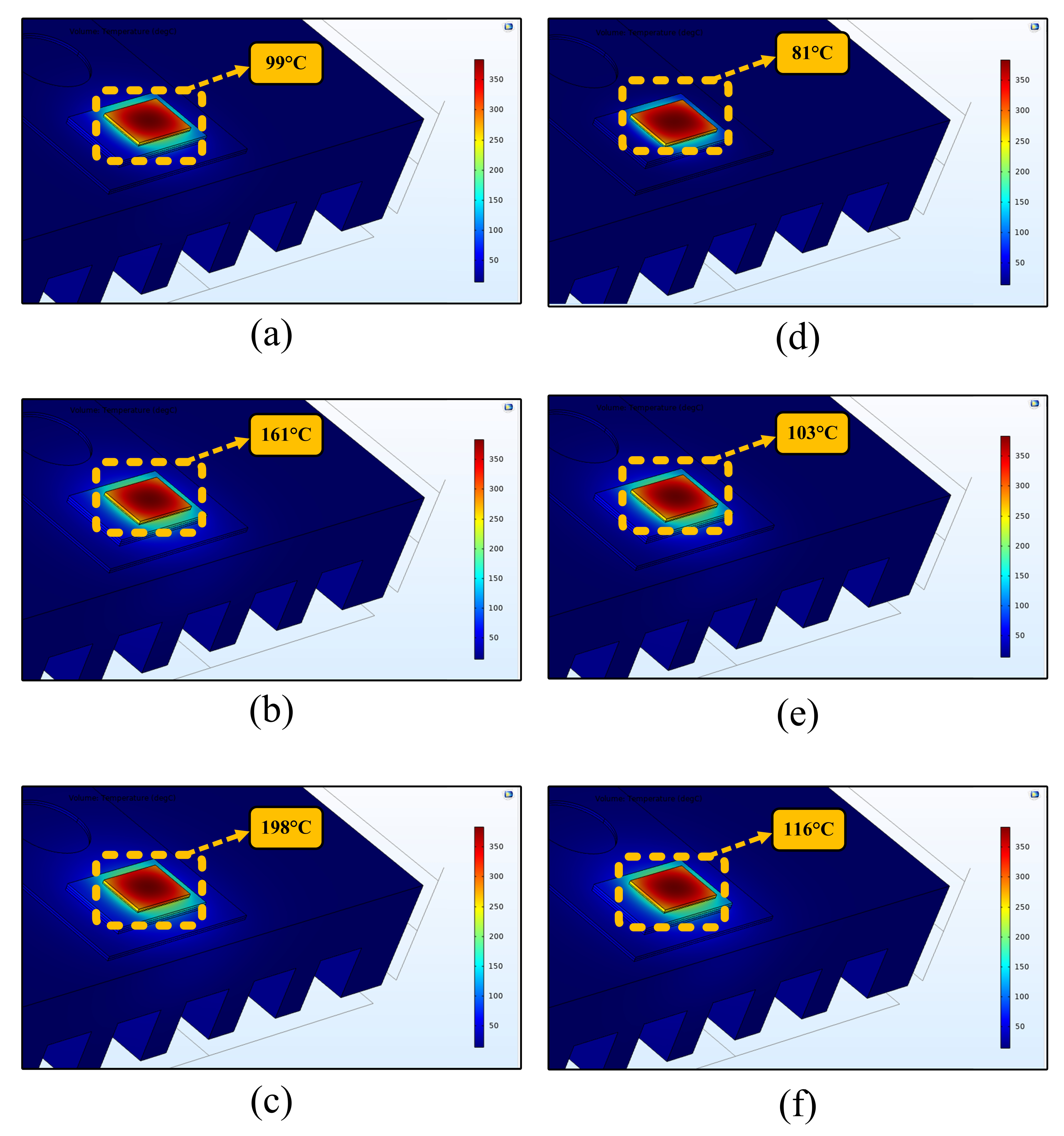
To verify the performance of the proposed method in simulation, a study in PSPICE is provided in this section (See the specifications in Table 3). According to (5) and Table 3, the value of the limited SCF current ( I S C L ) equals to 95 A, and the reference of the SCF current is set to 45 A, which is almost twice the load nominal current. Hence, during the SCF condition and after the delay interval, it is expected that the proposed method limits the SCF current to near 45 A. Figure 9 presents the IGBT waveforms in a temporary SCF. As seen, in the normal condition (during the pre-SCF and post-SCF time intervals) the IGBT current equals 22 A. As seen in the Figure 9a, in the temporary SCF condition (during the delay interval of the control loop) the SCF current is limited to near 90 A. After this time interval, the IGBT gate-emitter voltage is reduced to an appropriate value for controlling the SCF current to 45 A level (see Figure 9b). For the sustained SCF condition, the performance of the method is also examined where the temperature rise may violate the permissible value. In this case, the IGBT should be turned off after a predetermined time. Figure 10 shows the IGBTs waveform in a sustained SCF condition. As noticed, after 8 μ s , the IGBT is turned off to avoid thermal run-away. The main advantage here is that the IGBT reaches a 45 A SCF current, which is considerably less than the maximum SCF current in the device datasheet (160 A [39]). Therefore, the failure modes related to the turn-off process and high SC current value will be prevented.

3.2. FEM Simulation

In this section, Finite Element Method (FEM) is employed to investigate the behavioral differences of junction temperature profile during the SCFs. The 3D simulation model (see Figure 11) is developed in COMSOL Multiphysics based on the case study switch [39]. To improve simulation speed, the three metal external terminal pins of the switch are not simulated. Considering this simplification, the mesh size of the FEM model (see Figure 12) is more efficiently built. With the curvature factor of 0.5, values of 0.65 mm and 0.08 mm are considered as the maximum and minimum element size of the assigned mesh. The materials’ specifications of the simulated structure are shown in Table 4. The main employed boundary conditions are:
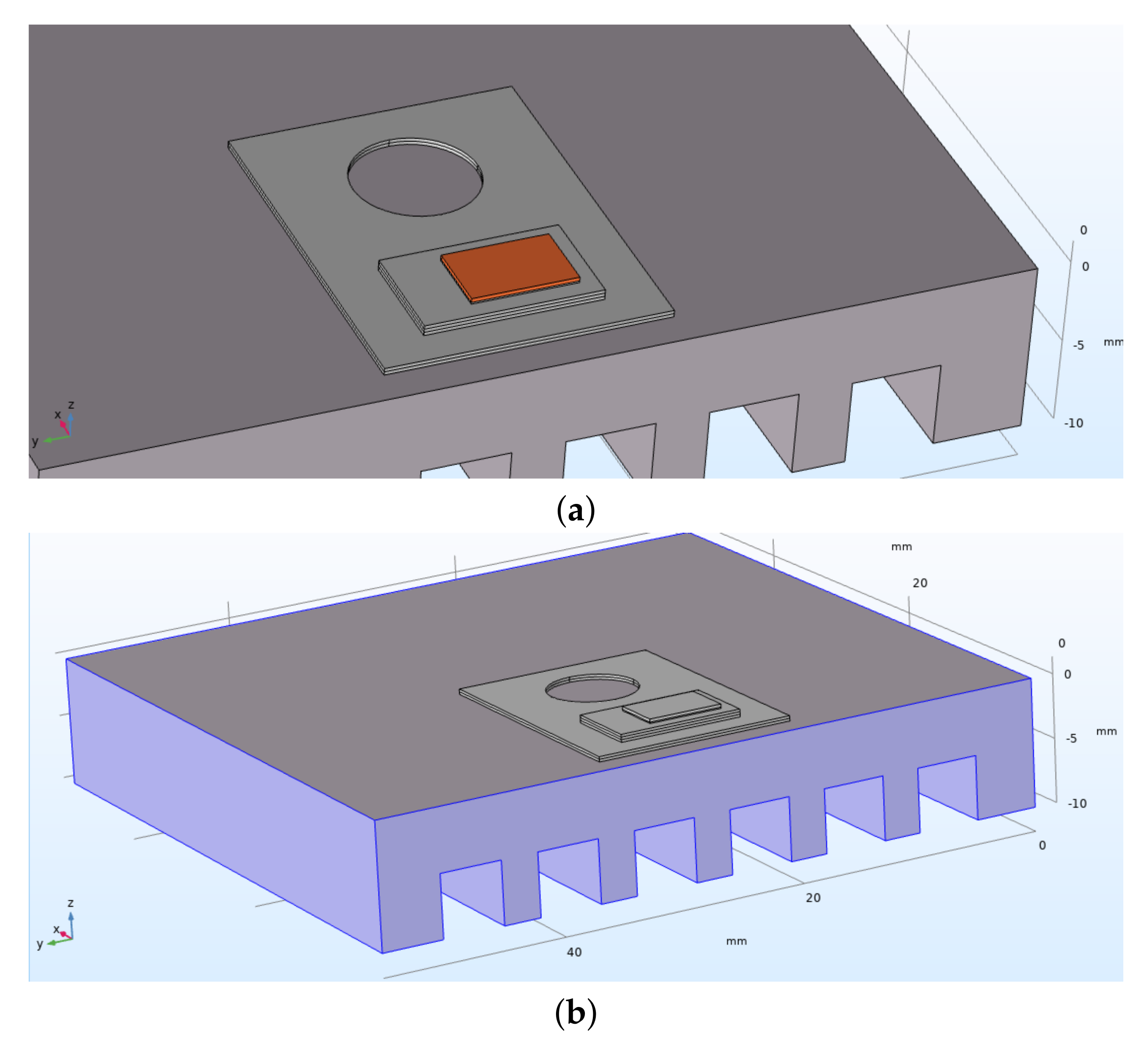
  • Boundary Heat Source: The chip area of the switch is considered as a heat source in short circuit condition (see Figure 13a). The value of the heat source is based on short circuit instantaneous power value ( P i n s ).
  • Heat flux: The simulated heat-sink on the bottom area of the switch is considered as the area from which the produced heat can be dissipated to the environment (see Figure 13b). Considering the employed heatsink in experimental implementation, the convective heat flux with heat transfer coefficient of 10,000 W/(m 2 · K ) is considered for the heatsink.
  • Initial Values: The initial temperature value of the IGBT is considered 75 C. This is the normal operation temperature of the IGBT in the pre-fault condition.
Using the above-explained developed simulation tool, the junction temperature of the switch is obtained in two conditions:
Condition 1: In this mode, no specific attempt is made for controlling the short circuit fault, and a 7 μ s SC fault with P i n s = 96 kW (regarding the device data-sheet [39]) is applied to the chip area.
Condition 2: In this mode, the proposed method is employed for controlling I S C . From t = 0 s to t = 200 ns , P i n s = 27 kW is applied to the IGBT chip area, and from t = 200 ns to t = 7 μ s , P i n s = 57 kW is applied.
In Figure 14, the IGBT short circuit power waveforms for the two conditions are shown based on short circuit time. The simulation values in condition 1 and condition 2 are based on Table 5. In Figure 15, the FEM results for these two conditions are shown. It can be seen that the average junction temperature of the switch in condition 1 reaches to 198 C, while in condition 2, the average junction temperature value is obtained 116 C. According to the case study switch datasheet [39], the maximum junction temperature of the switch is 175 C, meaning that the switch will be damaged during operation in condition 1. However, using the proposed method, the switch temperature is limited to 116 C, considerably smaller than the maximum allowable junction temperature. It is noteworthy that the junction temperature change after the SCF is lowered to one-third by our method. Therefore, in applications with considerable delayed protection for availability purposes, the proposed method is promising.

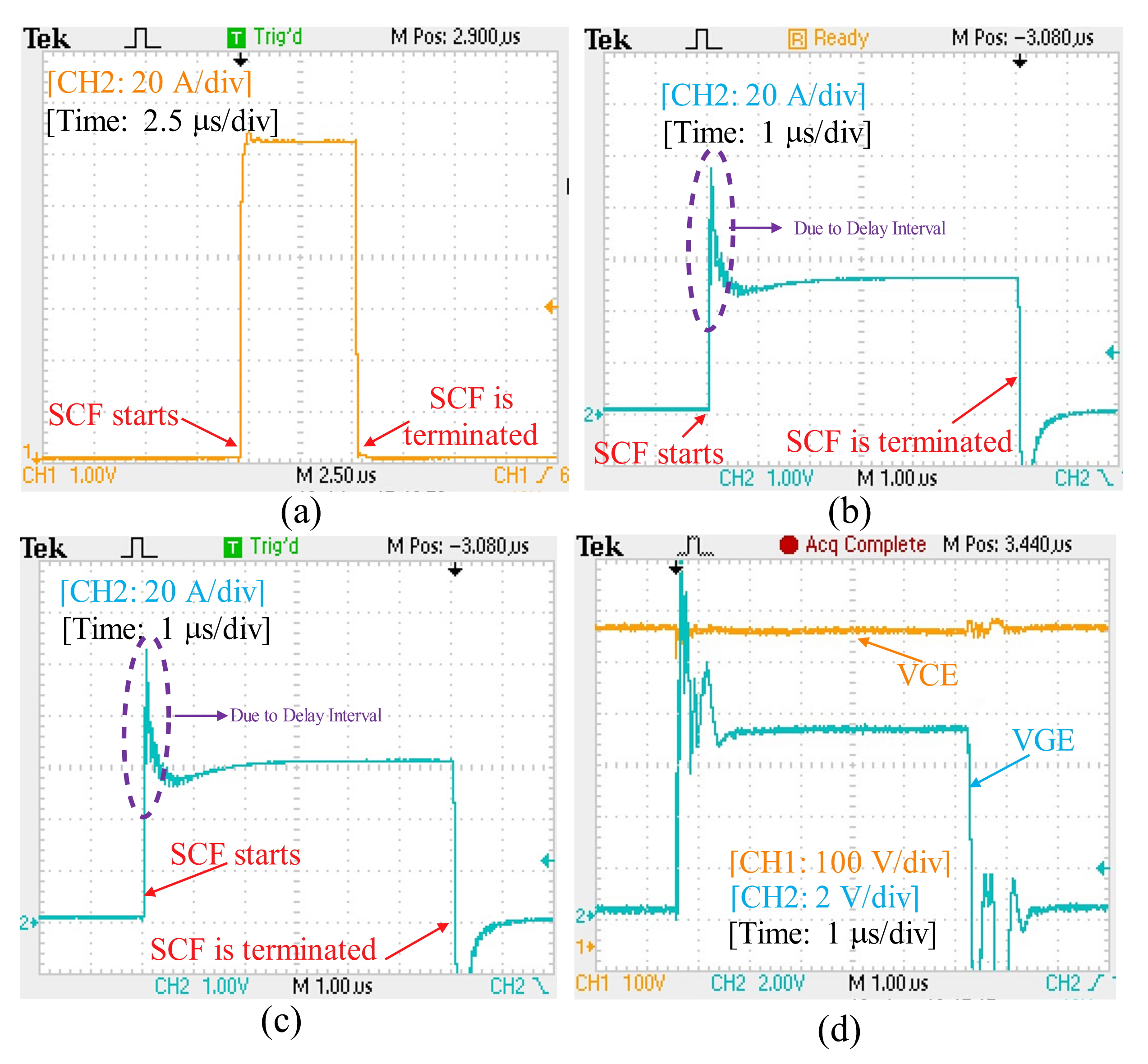
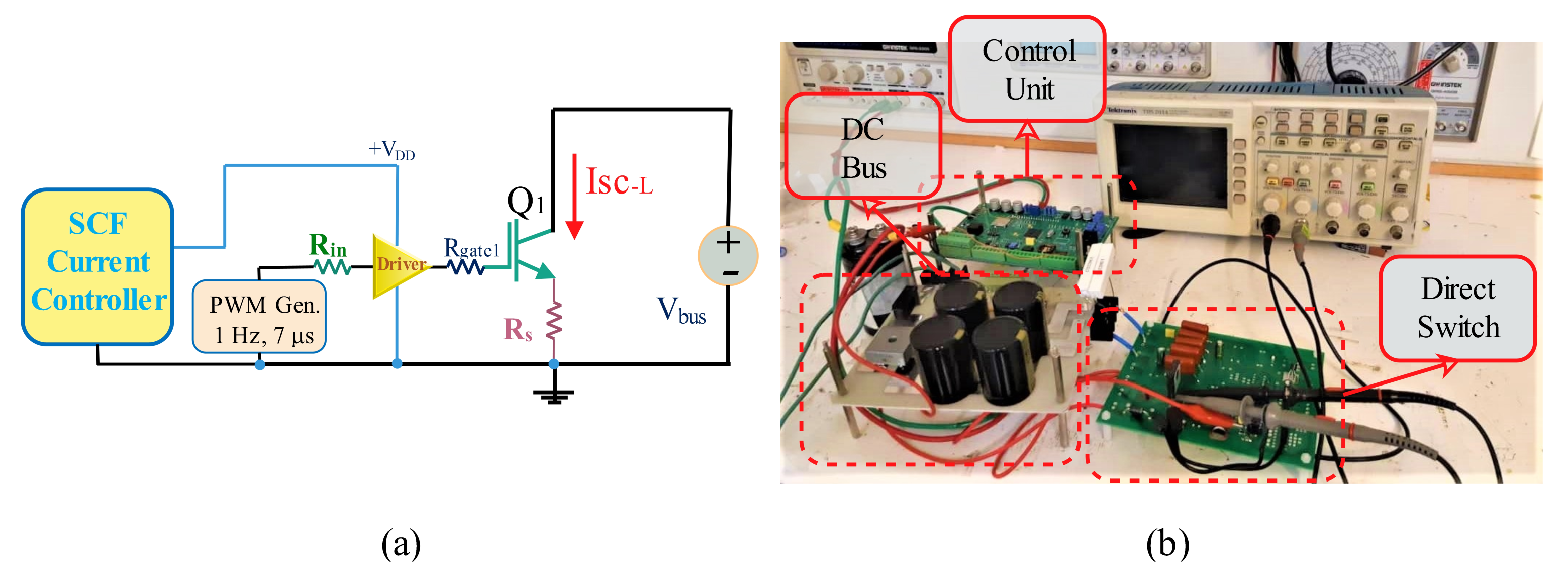
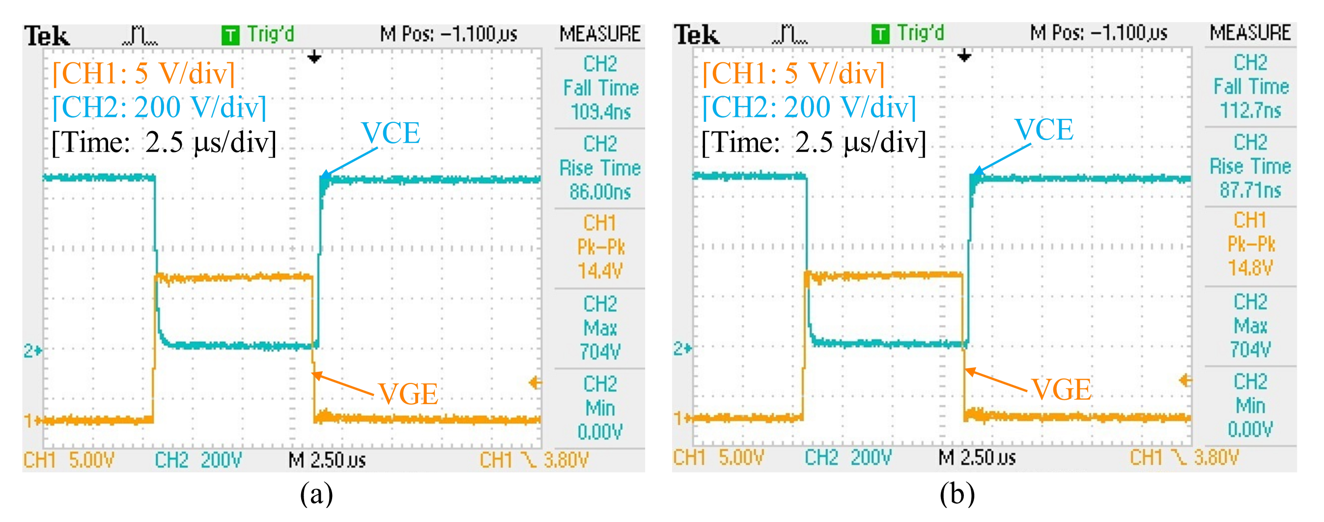
4. Experimental Results

An experimental prototype is implemented to examine the proposed method. The considered case for the experimental evaluation has the same specifications as the simulation analysis (see Table 3). In the tests, the IGBT is turned on in the SC condition. The block diagram of the experimental setup is provided in Figure 16a. The overview of the experimental setup is presented in Figure 16b. The SCF current is monitored by measuring the voltage drop across R S . At the first step, the SCF current is observed without the proposed method. To this end, the driver voltage is fixed to 15 V, and the SCF current is observed using a current transformer. In this condition, the SCF current is presented in Figure 17a. As seen, the SCF current amplitude equals 130 A without no attempt for limiting the current. In the second step, the limiting resistor as well as the control unit are added to the structure. The SCF current, when the SCF reference equals 50 A, is presented in Figure 17b, in which it can be observed that after the delay interval, the SCF current is properly controlled to a value equal 50 A. To validate the SCF current controller, SCF reference is slightly increased to 65 A (see Figure 17c).
Looking at Figure 17b,c, the SCF current can be controlled to values much less than the potential SCF current (130 A), which can limit the temperature rise in SCF conditions. Accordingly, the SCF current can be effectively limited to a value equal to twice the load nominal current by the proposed method. Figure 17d presents the gate-emitter and collector-emitter voltages of the IGBT under SCF condition, when the SCF is limited and controlled by the proposed method. Since the IGBT is turned on under the SCF condition, its collector-emitter voltage does not change from the turn-off state to the saturated region. The gate-emitter voltage, however, is decreased by the control unit to decrease the SCF current. As mentioned earlier, the proposed method does not slow down the device in the normal operation. Accordingly, Figure 18 shows the waveforms of the device in the normal operation. Regarding Figure 18, in the normal operation, the transient time intervals of the device with the proposed method (Figure 18a) and without the proposed method (Figure 18b) are approximately the same. Thus, it can be concluded that the proposed method does not affect the normal operation of the device. Considering Figure 18, the only difference is related to the high-level voltage of the IGBT’s gate-emitter where using the proposed method, this value is 0.5 V less than that of the condition without the proposed method.
In the experimental prototype, the switching frequency is 10 kHz, duty cycle is 7%, V B u s equals 700 V, and load current has a 10 A peak value. Thus, the average power approximately equals 490 W. The value of R S is 0.05, and its dissipating power equals 0.35 W, which is far less than the converter output power.
Finally, Table 6 compares the proposed method with extant methods. As can be seen, the proposed method has some advantages such as acceptable operation delayed operation, current controlling capability, and also does not have major effect on switch normal operation.

5. Conclusions

This paper proposed a novel SCF current limiting technique to enhance the IGBT reliability and maintain its seamless operation especially in applications where the risk of temporary SCFs is high. Using the proposed method, the SCF energy and the sudden temperature rise after the SCF condition are controlled by firstly limiting the SCF current using a small-value resistance in the device emitter, and secondly, controlling the SCF current to a predetermined SCF current using a simple PI control loop. The main advantage of the proposed control method is maintaining the normal IGBT operation with acceptable transient responses in turning on and turning off pulses. Our method substantially reduces the risk of IGBT failures due to the SCF energy and SCF peak current, which is normally the case in many applications. The performance of the method is validated via simulation, and FEM studies as well as the experimental setup results.

Author Contributions

Conceptualization, S.M.; methodology, S.M. and J.N.; software, S.M. and J.N.; validation, S.M. and J.N.; formal analysis, S.M.; investigation, S.M. and J.N.; resources, S.M., J.N. and K.M.; data curation, S.M., J.N.; writing—original draft preparation, S.M., J.N. and K.M.; writing—review and editing, S.M. and J.N.; visualization, S.M. and J.N.; supervision, K.M.; project administration, S.M. All authors have read and agreed to the published version of the manuscript.

Funding

This research is funded by the school of electronics engineering and computer science (EECS) at the Queen Mary University of London, London, UK.

Institutional Review Board Statement

Not applicable.

Informed Consent Statement

Not applicable.

Data Availability Statement

The data presented in this study are available on request from the corresponding author.

Conflicts of Interest

The authors declare no conflict of interest.

References

  1. Dieckerhoff, S.; Bernet, S.; Krug, D. Power loss-oriented evaluation of high voltage IGBTs and multilevel converters in transformerless traction applications. IEEE Trans. Power Electron. 2005, 20, 1328–1336. [Google Scholar]
  2. Xu, Z.; Li, M.; Wang, F.; Liang, Z. Investigation of Si IGBT Operation at 200 C for Traction Applications. IEEE Trans. Power Electron. 2013, 28, 2604–2615. [Google Scholar] [CrossRef]
  3. Mohsenzade, S.; Zarghani, M.; Kaboli, S. A high-voltage series-stacked IGBT switch with active energy recovery feature for pulsed power applications. IEEE Trans. Ind. Electron. 2019, 67, 3650–3661. [Google Scholar] [CrossRef]
  4. Zarghani, M.; Mohsenzade, S.; Kaboli, S. A series stacked IGBT switch based on a concentrated clamp mode snubber for pulsed power applications. IEEE Trans. Power Electron. 2019, 34, 9573–9584. [Google Scholar]
  5. Nasab, J.N.; Hadizade, A.; Mohsenzade, S.; Zarghany, M.; Kaboli, S. A Marx-based generator with adjustable FWHM using a controllable magnetic switch. IEEE Trans. Dielectr. Electr. Insul. 2019, 26, 324–331. [Google Scholar]
  6. Mohsenzade, S.; Zarghani, M.; Kaboli, S. A Series Stacked IGBT Switch to Be Used as a Fault Current Limiter in HV High Power Supplies. IEEE J. Emerg. Sel. Top. Power Electron. 2021, 9, 6300–6314. [Google Scholar] [CrossRef]
  7. Mohsenzade, S.; Zarghani, M.; Kaboli, S. A Voltage Balancing Method for Series-Connected IGBTs Operating as a Fault Current Limiter in High-Voltage DC Power Supplies. IEEE Trans. Ind. Electron. 2020, 68, 7895–7907. [Google Scholar] [CrossRef]
  8. Deng, E.; Wenzel, O.; Zhao, Z.; Zhang, Y.; Ying, X.; Li, J.; Huang, Y. Research on the Multi-Physics Field-Circuit Coupling Model of Press Pack IGBT Considering the Application of Hybrid HVDC Breakers. IEEE J. Emerg. Sel. Top. Power Electron. 2020, 9, 4854–4864. [Google Scholar] [CrossRef]
  9. Zhang, J.; Liu, J.; Zhong, S.; Yang, J.; Zhao, N.; Zheng, T.Q. A power electronic traction transformer configuration with low-voltage IGBTs for onboard traction application. IEEE Trans. Power Electron. 2018, 34, 8453–8467. [Google Scholar] [CrossRef]
  10. Zhao, X.; Li, B.; Fu, Q.; Mao, S.; Xu, D.; Leon, J.I.; Franquelo, L.G. DC solid state transformer based on three-level power module for interconnecting MV and LV DC distribution systems. IEEE Trans. Power Electron. 2020, 36, 1563–1577. [Google Scholar] [CrossRef]
  11. Choi, U.M.; Blaabjerg, F.; Lee, K.B. Study and handling methods of power IGBT module failures in power electronic converter systems. IEEE Trans. Power Electron. 2014, 30, 2517–2533. [Google Scholar] [CrossRef]
  12. Naghibi, J.; Mehran, K.; Foster, M.P. An Online Failure Assessment Approach for SiC-based MOSFET Power Modules Using Iterative Condition Monitoring Technique. In Proceedings of the 2020 IEEE 21st Workshop on Control and Modeling for Power Electronics (COMPEL), Aalborg, Denmark, 9–12 November 2020; pp. 1–5. [Google Scholar] [CrossRef]
  13. Harikumaran, J.; Buticchi, G.; Migliazza, G.; Madonna, V.; Giangrande, P.; Costabeber, A.; Wheeler, P.; Galea, M. Failure Modes and Reliability Oriented System Design for Aerospace Power Electronic Converters. IEEE Open J. Ind. Electron. Soc. 2021, 2, 53–64. [Google Scholar] [CrossRef]
  14. Chokhawala, R.S.; Catt, J.; Kiraly, L. A discussion on IGBT short-circuit behavior and fault protection schemes. IEEE Trans. Ind. Appl. 1995, 31, 256–263. [Google Scholar]
  15. Mohsenzade, S.; Zarghany, M.; Kaboli, S. A series stacked IGBT switch with robustness against short-circuit fault for pulsed power applications. IEEE Trans. Power Electron. 2017, 33, 3779–3790. [Google Scholar]
  16. Wu, R.; Blaabjerg, F.; Wang, H.; Liserre, M.; Iannuzzo, F. Catastrophic failure and fault-tolerant design of IGBT power electronic converters-an overview. In Proceedings of the IECON 2013—39th Annual Conference of the IEEE Industrial Electronics Society, Vienna, Austria, 10–13 November 2013; pp. 507–513. [Google Scholar]
  17. Reigosa, P.D.; Iannuzzo, F.; Rahimo, M.; Corvasce, C.; Blaabjerg, F. Improving the short-circuit reliability in IGBTs: How to mitigate oscillations. IEEE Trans. Power Electron. 2017, 33, 5603–5612. [Google Scholar] [CrossRef] [Green Version]
  18. Abbate, C.; Busatto, G.; Sanseverino, A.; Velardi, F.; Ronsisvalle, C. Analysis of low-and high-frequency oscillations in IGBTs during turn-on short circuit. IEEE Trans. Electron Devices 2015, 62, 2952–2958. [Google Scholar] [CrossRef]
  19. Lutz, J.; Basler, T. Short-circuit ruggedness of high-voltage IGBTs. In Proceedings of the 2012 28th International Conference on Microelectronics Proceedings, Nis, Serbia, 13–16 May 2012; pp. 243–250. [Google Scholar]
  20. Otsuki, M.; Onozawa, Y.; Kanemaru, H.; Seki, Y.; Matsumoto, T. A study on the short-circuit capability of field-stop IGBTs. IEEE Trans. Electron Devices 2003, 50, 1525–1531. [Google Scholar] [CrossRef]
  21. Yang, F.; Tan, J.; Lu, S.; Zhu, Y. Investigation on the robustness during short-circuit turn-off and its tradeoff characteristics with performance in IGBTs. IEEE Trans. Electron Devices 2017, 64, 3293–3297. [Google Scholar]
  22. Basler, T.; Bhojani, R.; Lutz, J.; Jakob, R. Measurement of a complete HV IGBT IV-characteristic up to the breakdown point. In Proceedings of the 2013 15th European Conference on Power Electronics and Applications (EPE), Lille, France, 2–6 September 2013; pp. 1–9. [Google Scholar]
  23. Basler, T.; Bhojani, R.; Lutz, J.; Jakob, R. Dynamic self-clamping at short-circuit turn-off of high-voltage IGBTs. In Proceedings of the 2013 25th International Symposium on Power Semiconductor Devices & IC’s (ISPSD), Kanazawa, Japan, 26–30 May 2013; pp. 277–280. [Google Scholar]
  24. Kopta, A.; Rahimo, M.; Schlapbach, U.; Kaminski, N.; Silber, D. Limitation of the short-circuit ruggedness of high-voltage IGBTs. Proceeding of the 2009 21st International Symposium on Power Semiconductor Devices & IC’s, Barcelona, Spain, 14–18 June 2009; pp. 33–36. [Google Scholar]
  25. Muller, A.; Pfirsch, F.; Silber, D. Trench IGBT behaviour near to latch-up conditions. In Proceedings of the ISPSD’05—the 17th International Symposium on Power Semiconductor Devices and ICs, Santa Barbara, CA, USA, 23–26 May 2005; pp. 255–258. [Google Scholar]
  26. Reigosa, P.D.; Iannuzzo, F.; Corvasce, C.; Rahimo, M. Modeling of IGBT With High Bipolar Gain for Mitigating Gate Voltage Oscillations During Short Circuit. IEEE J. Emerg. Sel. Top. Power Electron. 2019, 7, 1584–1592. [Google Scholar]
  27. Spirito, P.; Maresca, L.; Riccio, M.; Breglio, G.; Irace, A.; Napoli, E. Effect of the collector design on the IGBT avalanche ruggedness: A comparative analysis between punch-through and field-stop devices. IEEE Trans. Electron Devices 2015, 62, 2535–2541. [Google Scholar] [CrossRef] [Green Version]
  28. Voss, S.; Schulze, H.J.; Niedernostheide, F.J. Optimization of the temperature dependence of the anode-side current gain of IGBTs by field-stop design. In Proceedings of the 2010 22nd International Symposium on Power Semiconductor Devices & IC’s (ISPSD), Hiroshima, Japan, 6–10 June 2010; pp. 141–144. [Google Scholar]
  29. Chen, Y.; Li, W.; Iannuzzo, F.; Luo, H.; He, X.; Blaabjerg, F. Investigation and classification of short-circuit failure modes based on three-dimensional safe operating area for high-power IGBT modules. IEEE Trans. Power Electron. 2017, 33, 1075–1086. [Google Scholar]
  30. John, V.; Suh, B.S.; Lipo, T.A. Fast-clamped short-circuit protection of IGBT’s. IEEE Trans. Ind. Appl. 1999, 35, 477–486. [Google Scholar] [CrossRef]
  31. Chen, M.; Xu, D.; Zhang, X.; Zhu, N.; Wu, J.; Rajashekara, K. An improved IGBT short-circuit protection method with self-adaptive blanking circuit based on V CE measurement. IEEE Trans. Power Electron. 2017, 33, 6126–6136. [Google Scholar] [CrossRef]
  32. Sathik, M.H.M.; Sundararajan, P.; Sasongko, F.; Pou, J.; Vaiyapuri, V. Short Circuit Detection and Fault Current Limiting Method for IGBTs. IEEE Trans. Device Mater. Reliab. 2020, 20, 686–693. [Google Scholar] [CrossRef]
  33. Wang, Z.; Shi, X.; Tolbert, L.M.; Wang, F.; Blalock, B.J. A di/dt feedback-based active gate driver for smart switching and fast overcurrent protection of IGBT modules. IEEE Trans. Power Electron. 2013, 29, 3720–3732. [Google Scholar] [CrossRef]
  34. Oinonen, M.; Laitinen, M.; Kyyrä, J. Current measurement and short-circuit protection of an IGBT based on module parasitics. In Proceedings of the 2014 16th European Conference on Power Electronics and Applications, Lappeenranta, Finland, 26–28 August 2014; pp. 1–9. [Google Scholar]
  35. Radun, A. An alternative low-cost current-sensing scheme for high-current power electronics circuits. IEEE Trans. Ind. Electron. 1995, 42, 78–84. [Google Scholar]
  36. Ammous, A.; Allard, B.; Morel, H. Transient temperature measurements and modeling of IGBT’s under short circuit. IEEE Trans. Power Electron. 1998, 13, 12–25. [Google Scholar]
  37. Lobsiger, Y.; Kolar, J.W. Closed-Loop di/dt and dv/dt IGBT Gate Driver. IEEE Trans. Power Electron. 2014, 30, 3402–3417. [Google Scholar] [CrossRef]
  38. Yang, X.; Yuan, Y.; Long, Z.; Goncalves, J.; Palmer, P.R. Robust stability analysis of active voltage control for high-power IGBT switching by Kharitonov’s theorem. IEEE Trans. Power Electron. 2015, 31, 2584–2595. [Google Scholar] [CrossRef]
  39. Infineon Technologies. Highspeed Duo-Pack IGBT, IKW40N120H3, 1200 V, 40 A, PG-TO247-3 Package. 2014. Available online: https://www.infineon.com/cms/en/product/power/igbt/igbt-discretes/ikw40n120h3/ (accessed on 30 July 2021).
Figure 1. The schematic of the proposed method for limiting IGBT peak current.
Energies 14 07397 g001
Figure 2. (a) The ratio of P l o s s to P o u t , and (b) the ratio of I S C L to I S C as the functions of R S .
Energies 14 07397 g002
Figure 3. The schematic overview of the SCF current controlling method.
Energies 14 07397 g003
Figure 4. The control signals of the proposed method in normal and SCF conditions.
Energies 14 07397 g004
Figure 5. IGBT current profile using the proposed method.
Energies 14 07397 g005
Figure 6. Schematic overview of the proposed method.
Energies 14 07397 g006
Figure 7. The simplified IGBT model valid in active region.
Energies 14 07397 g007
Figure 8. The Bode diagram of the SCF current controller.
Energies 14 07397 g008
Figure 9. IGBTs waveforms for a temporary SCF, (a) IGBT current, and (b) IGBT gate-emitter voltage.
Energies 14 07397 g009
Figure 10. IGBT I S C and V G E waveforms for a sustained SCF condition.
Energies 14 07397 g010
Figure 11. 3D simulated structure of case study IGBT switch in COMSOL; (a) overall structure with packaging, and (b) internal structure of the switch with layered structure.
Energies 14 07397 g011
Figure 12. Assigned mesh for the 3D structure of the switch in FEM solutions.
Energies 14 07397 g012
Figure 13. (a) Heat source in the chip area (red color), and (b) heat flux on the bottom area of the heatsink (blue area), as the main considered boundary conditions.
Energies 14 07397 g013
Figure 14. The SCF power using the proposed method and the case without any attempt to limit SCF current.
Energies 14 07397 g014
Figure 15. Thermal distribution of case study IGBT in condition 1 at (a) t = 1 μ s , (b) t = 4 μ s , (c) t = 7 μ s , and for condition 2 at (d) t = 1 μ s , (e) t = 4 μ s , (f) t = 7 μ s .
Energies 14 07397 g015
Figure 16. (a) The block diagram and (b) the photo of the experimental setup.
Energies 14 07397 g016
Figure 17. The experimental waveforms of (a) SCF current without applying the proposed method, (b) SCF current using the proposed method when SCF reference equals 50 A, (c) SCF current using the proposed method when SCF reference equals 65 A, and (d) gate-emitter and collector-emitter voltages of the IGBT.
Energies 14 07397 g017
Figure 18. The transient time intervals of the device (a) with the proposed method and (b) without the proposed method.
Energies 14 07397 g018
Table 1. The specifications of the considered case for current limiting.
ParameterValue
IGBT Part NumberIKW40N120H3
Nominal Current30 A
g f s 20 S
V t h 5.5 V
V D D 15 V
Maximum SC Current160 A
P o u t 1000 W
Table 2. The required parameters for the stability analysis.
ParameterValue
g f s 20 S
R S 0.05 Ω
C C E 55 pF
C C G 72 pF
C G E 3.8 pF
R g i n t 15 Ω
R O 55 Ω
L g 30 nH
L C 20 nH
L E 15 nH
Table 3. The specifications of the considered case for simulation.
IGBT part numberIKW40N120H3
Gate driver ICLM5111
Op. Amp ICLM7171
Nominal Current22 A
Blocking Voltage600 V
V D D m a x 15 V
R S 0.05 Ω
Table 4. Material specifications in the developed simulation model of IGBT.
MaterialThermal ConductivityHeat CapacityDensity
[ W / ( m · K ) ][ J / ( kg · K ) ][ kg / m 3 ]
Aluminium (Al)2399102699
Copper (Cu)385380180
Silicon (Si)1317002330
Solder (SnAgCu)601607400
Ceramic (Al 2 O 3 )277763900
Epoxy Mold0.39001250
Table 5. Parameters of the studied case study SC condition for FEM simulation.
ParameterValue
t D 200 ns
V b u s 600 V
I S C 160 A
I S C L 95 A
I S C r e f 45 A
t S C 7 μ s
Table 6. Material specifications in the developed FEM model of SiC MOSFET power module.
Feature/Item[15][30,31][33,34][6][7]Proposed Method
Delay200 ns1∼5 μ sLess than 100 ns200 ns300 ns200 ns
SC Current limitingYesNoNoYesYesYes
SC Current controllingNoNoNoNoYesYes
Effects on normal operationNoNoNoNoYesNo
Publisher’s Note: MDPI stays neutral with regard to jurisdictional claims in published maps and institutional affiliations.

