Article

Transformer-Less Switched-Capacitor Quasi-Switched Boost DC-DC Converter

1
Department of Electrical Engineering, Chonnam National University, Gwangju 61186, Korea
2
Faculty of Electrical and Electronics Engineering, Ho Chi Minh City University of Technology and Education, Ho Chi Minh City 700000, Vietnam
3
Faculty of Electrical Engineering Technology, Industrial University of Ho Chi Minh City, Ho Chi Minh City 700000, Vietnam
*
Authors to whom correspondence should be addressed.
Energies 2021, 14(20), 6591; https://doi.org/10.3390/en14206591
Submission received: 7 September 2021 / Revised: 9 October 2021 / Accepted: 10 October 2021 / Published: 13 October 2021
(This article belongs to the Special Issue Energy Conversion and Operation Technologies for Smart Grid)

Abstract

:
In this article, a quasi-switched boost converter based on the switched-capacitor technique with high step-up voltage capability is dealt with and analyzed. The proposed converter offers a simple structure and low voltage stress on the semiconductor elements with intrinsic small duty cycle. An inductor of the proposed converter is connected in series with the input voltage source; therefore, continuous input current ripple is attainable. In addition, the efficiency of the proposed converter is also improved. A detailed steady-state analysis is discussed to identify the salient features of the switched-capacitor-based quasi-switched boost DC-DC converter. The performance of the converter is compared against similar existing high boost DC-DC converters. Finally, the switched-capacitor-based quasi-switched boost DC-DC converter is investigated by experimental verification.

1. Introduction

Nowadays, the deployment of the renewable energy sources includes photovoltaic, and fuel cells have grown significantly over the past decade. However, one of the main drawbacks of these sources are low output voltage. As a main part of the distributed generation technologies, the high-voltage boost DC-DC converters have emerged and been the main link to realize an energy transfer from the renewable energy sources [1,2]. Typical isolated converters have been developed to achieve a high voltage conversion with high turns ratio of the high-frequency transformer. Isolated converters including forward, flyback, half/full-bridge, and push–pull structures were presented in [3,4,5,6]. However, they offer problems such as leakage inductance occurred by the secondary side of the HF transformer, showing large voltage and current spikes on semiconductor devices. By contrast, the transformer-less high voltage gain DC-DC configurations are considering suitable solutions for achieving high conversion efficiency and decreasing the cost of system in the power distributed system due to omitting the galvanic isolation transformers. The coupled-inductor-based structures can also produce the solution to improve the voltage gain without galvanic isolation [7,8]. Nonetheless, these converters have to add a snubber-clamped circuitry to reduce leakage inductor energy recovery problems, which increases the cost of the converter.
For the transformer-less DC-DC structures, a conventional boost DC-DC converter is able to provide a boost ability. In the ideal case, the boost converter can realize very high voltage gain. However, the duty cycle is limited due to the non-idealities of the passive components, semiconductor devices, and loss considerations. Therefore, the conventional boost converter is not a suitable solution for high voltage gain applications. In such applications, the cascaded and quadratic boost converters were introduced to achieve high voltage conversion [9,10]. In this case, two or more conventional boost converters are connected in series. The size and weight of these converters will be increased because many switches and gate drivers are required. Furthermore, the voltage conversion of the converter can also be improved by using the switched-inductor technology in [11,12,13]. In the conventional switched-inductor high step-up DC-DC converter, the voltage gain is limited and the semiconductor devices with high voltage ratings are needed, which significantly raises the cost and the size of the converter. The duty cycle of the mentioned conventional boost non-isolated DC-DC is operated in wide range, and the range of duty cycle is varied between 0 and 1. In this case, the high voltage gain can be obtained with large duty cycle value, which causes to produce power loss on power active switches. Moreover, to limit the range of duty cycle operated within (0, 0.5) and improve the voltage gain, the Z-source and quasi-Z source configurations are considered as good solutions [14,15,16,17]. The shortages of these topologies are discontinuous input current and complex topological structure. Instead of considering about adding passive components in the class of the Z-source and quasi-Z-source-based converters, a class of switched-boost and quasi-switched-boost converters were proposed in [18,19]. However, the voltage stress on the semiconductor devices of them is still high and equals to the output voltage. The aforementioned structures can realize high voltage conversion but share a similar problem, which is the requirement of a large number of additional devices. In addition, research of switched-capacitor-based technology has been proposed to produce the high voltage gain, as presented in [20,21,22,23,24]. The switched-capacitor structure has been known with merits such as small size, low-voltage rating on the semiconductor devices, and high voltage density. In [21], a boost DC-DC converter adopting the switched-boost network was introduced with high voltage conversion and low voltage rating on switches. However, the voltage and current stress of diodes are still high. In [22], an extended switched-boost DC-DC was proposed, which incorporated the switched-capacitor network and switched-boost converter with improved the voltage gain and low voltage stress on semiconductor devices [22]. Nevertheless, the input current is discontinuous and the voltage ratio is still not high. The dual-switch boost converter based on the switched-capacitor in [23] has used for one inductor structure, high boost gain, and low voltage stress. However, the input research in [24] has been proposed the solution for the high-step-up topology. By applying an additional diode and capacitor, the voltage charge pumping solution with integrating switched-boost and Z-source networks have been developed with high voltage gain and low voltage rating on components.
In this article, to enhance the practical high-voltage conversion and reduce the duty cycle ratio, a new transformer-less quasi-switched boost DC-DC converter with integrating switched-capacitor network will be determined. The proposed switched-capacitor switched-boost converter has the merit of enhancing voltage gain, achieve low voltage rating on the active switches and high efficiency. The remainder of this article is organized as follows. Section 2 presents the configuration and operating principle of the switched-capacitor quasi-switched boost converter in both continuous conduction mode (CCM) and discontinuous conduction mode (DCM). In Section 3, the design guideline is explained. The comparison between proposed converter and other high gain topologies is provided in Section 4. Further, the experimental verifications are presented in Section 5. Finally, Section 6 concludes this article.

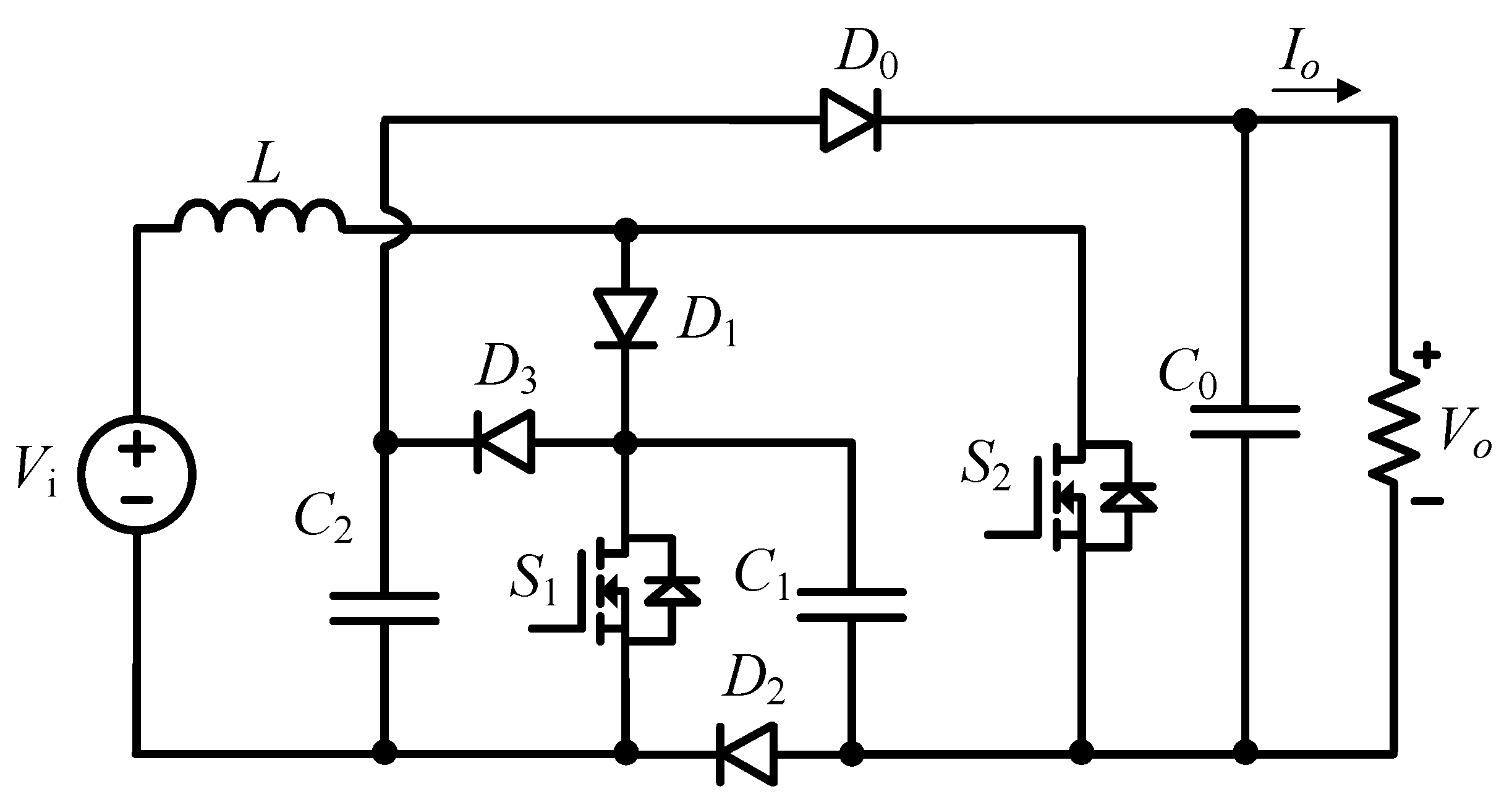
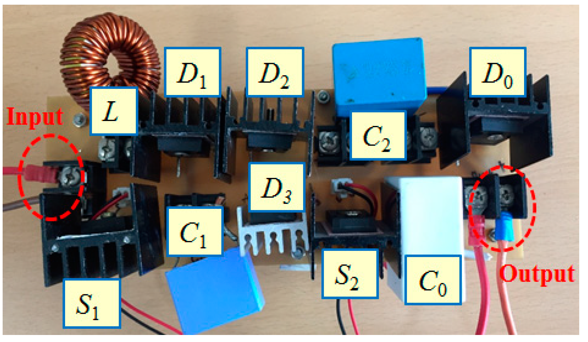
2. Operating Principle of Proposed SCQSBC

2.1. Power Circuit

The configuration of the proposed SCQSBC converter as depicted in Figure 1 incorporates the quasi-switched boost network and switched-capacitor cell. The converter is composed of two MOSFETs (S1 and S2), four diodes (D0 to D3), one inductor, and three capacitors (C0 to C2). Figure 2 presents the typical waveforms of the SCQSBC in CCM and DCM. In this case, it can be seen that S1 is turned on 50% of the period, while S2 is turned on with the duty cycle of D.

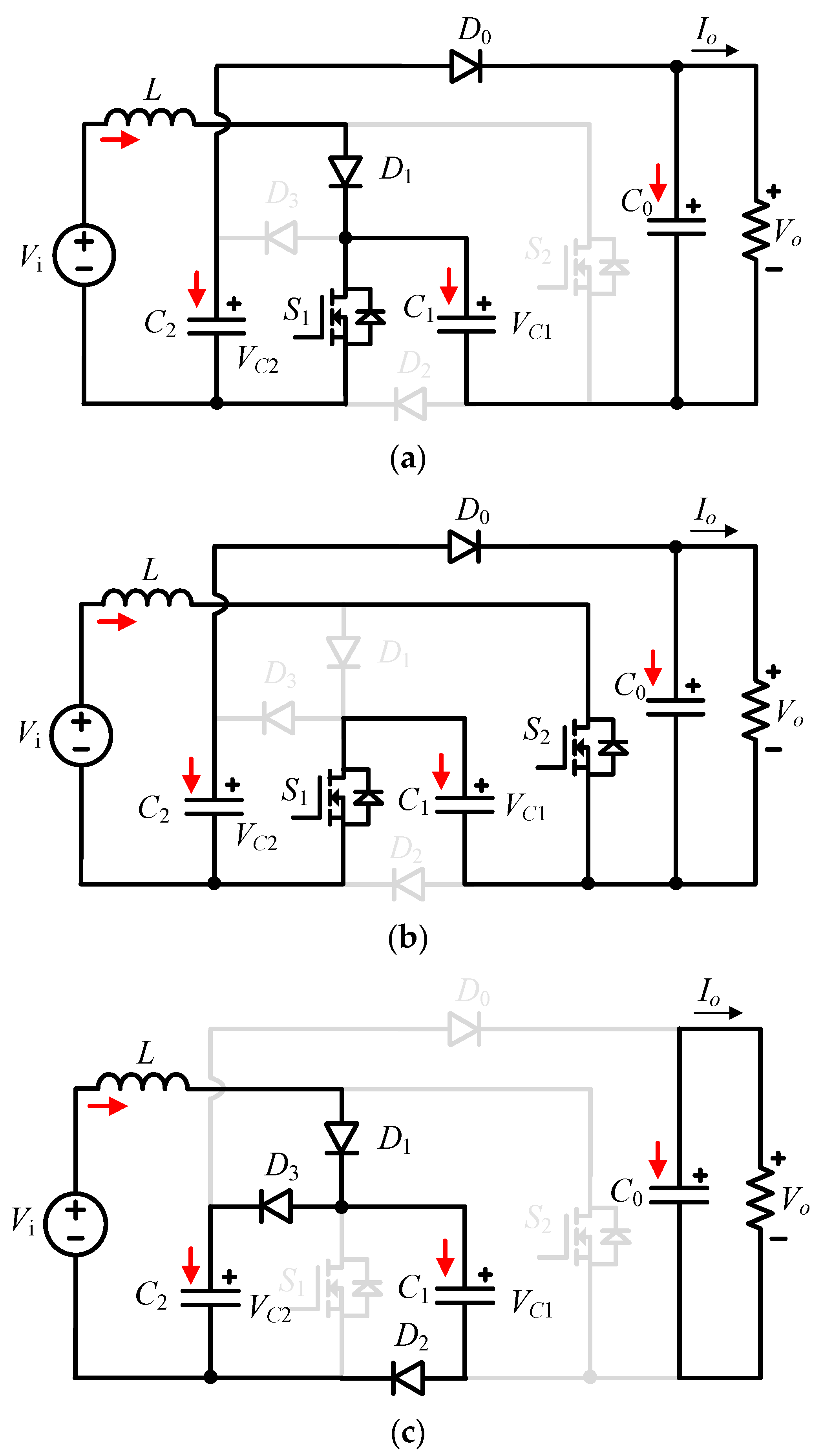
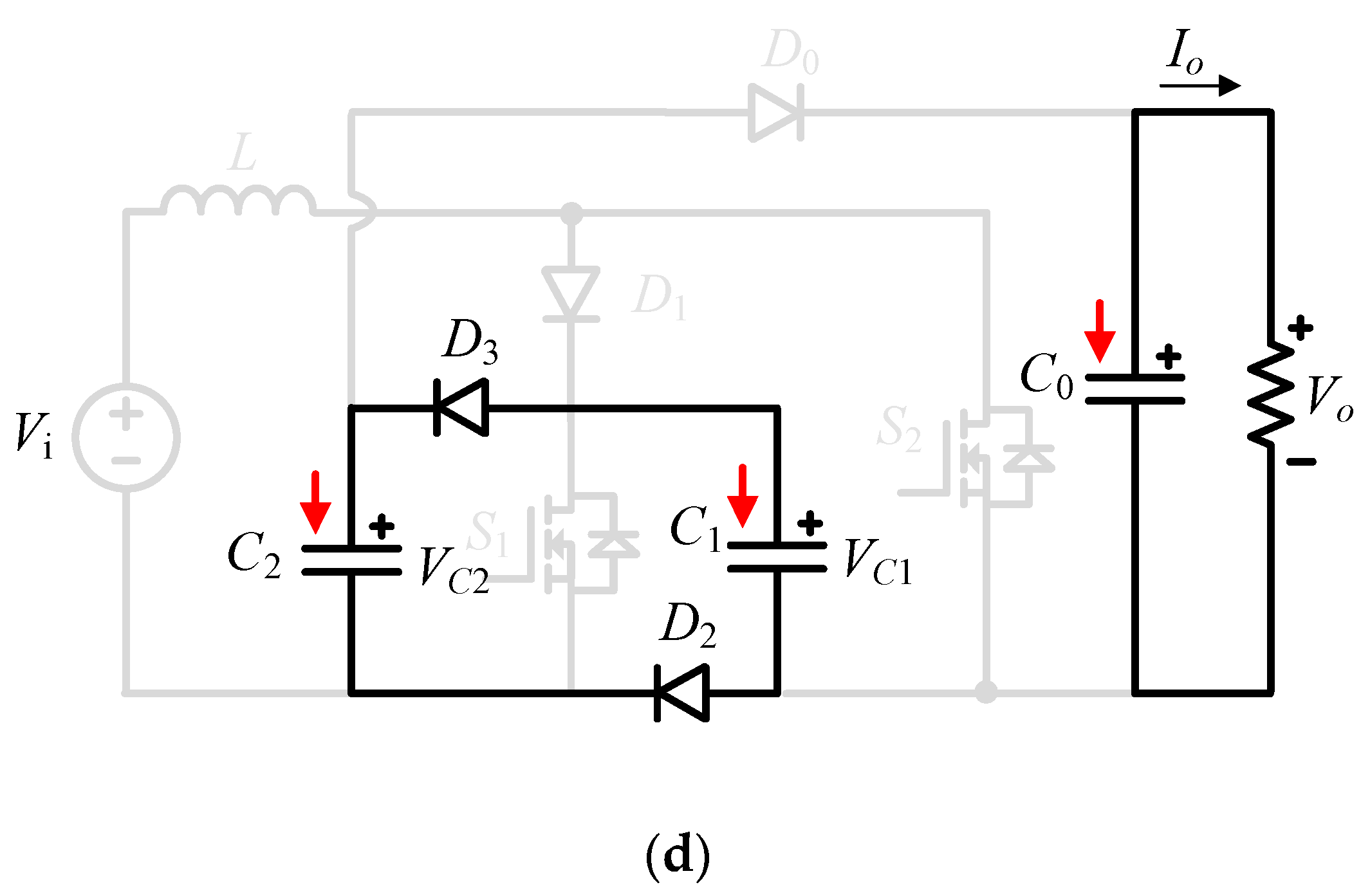
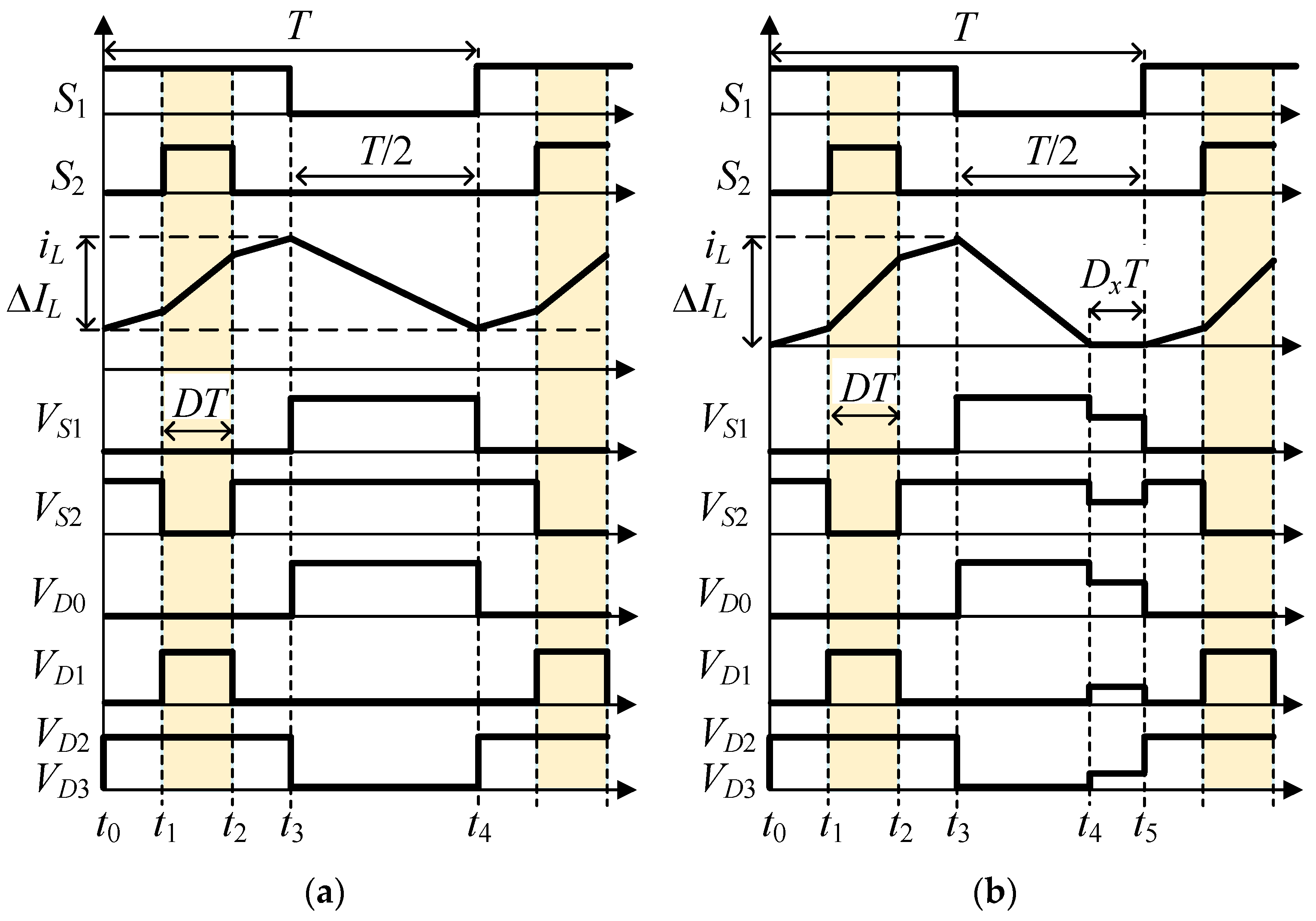
2.2. Circuit Analysis in CCM

To determine the operating analysis of the SCQSBC in the CCM, assume that (1) all power components are ideal; (2) capacitors C0, C1, and C2 are enough to induce the constant voltage in one switching period; and (3) the current of an inductor is linear.
Mode I (t0t1 and t2t3): In this mode, the inductor is magnetized by input power supply. MOSFET S1 is turned on while MOSFET S2 is turned off. Capacitors C1 and C2 are discharged through the output C0 capacitor. During this mode, diodes D0 and D1 are forward-biased, while diodes D2 and D3 are reverse-biased. The analysis circuitry of the SCQSBC is depicted in Figure 3a. The following equations can be given:
{ v L = V i i C 01 + i C 11 = I o
Mode II (t1t2): In this mode, the inductor is still magnetized by input power supply and capacitor C1. MOSFETs S1 and S2 are turned on. Capacitors C1 and C2 are also discharged through the output C0 capacitor. During this mode, diode D0 is forward-biased, whereas diodes D1, D2 and D3 are reverse-biased. The circuitry of the SCQSBC is depicted in Figure 3b. The equations can be obtained:
{ v L = V i + V C 1 i C 02 + i C 12 = I o i C 22 i C 12 = I L
Mode III (t3t4): In this mode, the inductor is discharged in series with the input voltage to charge two capacitors C1 and C2, while MOSFETs S1 and S2 are turned off. During this mode, the diodes D0 is reversed-bias, whereas diodes D1, D2 and D3 are forward-biased. Capacitor C0 is transferred an energy through the resistive load. The circuitry of the SCQSBC is depicted in Figure 3c. The mentioned equations are given:
{ v L = V i V C 1 i C 03 = I o i C 13 = I L i C 23
From (1) to (3), the average value of the inductor voltage can be obtained:
L d i L d t = ( 0.5 D ) V i + D ( V i + V C ) + 0.5 ( V i V C ) = 0
Applying the DC variable equation to (4), the capacitors voltage and voltage gain of the proposed SCQSBC can be given as follows:
{ V C 1 = V C 2 = V C = 2 1 2 D V i G = V o V i = 4 1 2 D
where D is the duty cycle.
An inductor of the proposed SCQSBC is connected directly with an input voltage source, and the expressions of the inductor current is:
I L = 4 1 2 D I o
From (1) to (3), the currents of capacitors C0, C1 and C2 in mode I, II and III are derived as follows, respectively.
{ i C 01 = I o k C 1 i C 11 = i C 21 = k C k C 1 I o
{ i C 02 = k C 2 + 2 D 2 D ( k C 1 ) I o i C 12 = 2 k C + 4 D 8 k C D + 4 k C D 2 2 D ( k C 1 ) ( 1 2 D ) I o i C 22 = 2 k C 2 D 2 D ( k C 1 ) I o
{ i C 03 = I o i C 13 = 2 ( 1 + 2 D ) ( 1 2 D ) I o i C 23 = 2 I o
k C = C 2 r C 2 % 2 C 0 r C 0 %
where kC, rC0%, and rC2% are the ratio of capacitor C2 and C0 currents in mode I, voltage ripple of capacitors C0 and C2, respectively.
In mode I, the capacitor C2 and C0 currents are determined as:
{ i C 03 = C 2 Δ V C ( 0.5 D ) T = C 2 r C 2 % V C ( 0.5 D ) T i C 13 = i C 23 = C 0 Δ V o ( 0.5 D ) T = C 0 r C 0 % V o ( 0.5 D ) T

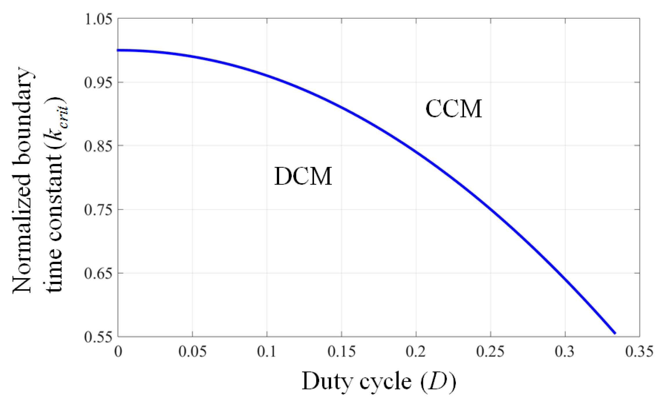
2.3. Circuit Analysis in DCM

The SCQSBC is operated in DCM when the light load of converter is applied. The operating of the proposed SCQSBC for DCM analysis is verified in four modes. First when switch S1 is only turned on, second when S1 and S2 are on simultaneously, third when S1 and S2 are turned off and an inductor current is nonzero, and fourth when the S1 and S2 are turned off and an inductor current is zero. The inductor current reduces to zero at time t4. As shown in Figure 2b, intervals t0t1 and t2t3 are mode I, interval t1t2 is mode II, interval t3t4 is mode III, and interval t4-t5 is mode IV. Note that the converter is operated in CCM in mode I to mode III.
Mode I (t0t1 and t2t3): For this mode, the operating of the proposed SCQSBC and equivalent circuit are the same as CCM mode I and also depicted in Figure 3a. From the starting point of this mode (time t0 and t2t3), the inductor current increases linearly from zero and achieves the maximum value at t3. The current ripple of inductor in each mode is given:
Δ I 1 = Δ I 3 = V i 2 L ( 0.5 D ) T
Mode II (t1t2): For the mode, the operating of the proposed SCQSBC and circuitry is the CCM analysis mode II. The current ripple of inductor in this mode can be given:
Δ I 2 = ( V i + V C L ) D T
The maximum current through inductor can be given as follows:
I L , m a x = ( V i / 2 + D V C L ) T
Mode III (t3t4): For the mode, the operating of the proposed SCQSBC and equivalent circuit are the same as CCM mode III. The current ripple of inductor in this mode can be given:
Δ I 4 = ( V i V C L ) D x T
Mode IV (t4t5): The equivalent circuit is depicted in Figure 3c. Switches S1 and S2 are remained off and inductor current is at zero level. The capacitor Co is discharged through resistive load.
According to the condition of CCM/DCM boundary, we have:
I L ¯ < Δ I L / 2
The result of the substitution of (6)–(9) into (11) is as follows:
k < k c r i t ( D )
where k is a normalized boundary of the converter in DCM, and k = 36L/(RT), kcrit = 1 − 4D2.
Figure 4 presents the relationship of kcrit and D; the DCM and CCM boundary region is depicted. Then, the converter operates in CCM at the value k > kcrit.
Referring to Figure 2b, the average value of inductor current is given by:
I L ¯ = Δ I 1 ( 1 2 + 2 D x ) + Δ I 2 ( 1 4 + D x 2 )
According to the volt-second balance property of inductor to (13), Dx is calculated:
D x = V i / 2 + D V C 2 ( V C V i )
From (6), (18), and (19), the output voltage conversion of the SCQSBC in DCM can be verified by:
G = 2 k + 1 2 D + 4 k 2 + ( 1 4 D 2 ) 2 2 [ k D ( 1 2 D ) ( 1 + D ) ]

3. Designed Guideline

3.1. Selection of Inductor

The rated current of inductor can be determined as the input current and given by (6). The inductor value is selected such that the proposed SCQSBC operates in CCM. Considering the operating mode 2 shown in Figure 3c, the ripple current expression for inductor is given as:
Δ I L = V C V i 2 L f s
Assuming from (4) and (5) that Δ I L = r L % I L , inductance L in the function of inductor current ripple is:
L = ( 1 + 2 D ) V i 2 2 ( 1 2 D ) r L % f s P o
where rL%, T, and Po are the inductor current ripple, period, and output power, respectively.

3.2. Selection of Capacitors

Like the parameter design guideline of the inductor, the design of the capacitors can be determined by the rated voltage and capacitance. The rated voltages of the capacitors can be determined from (5). The capacitors in the proposed SCQSBC are designed based on the differential equation of capacitors C0, C1, and C2.
{ C 1 Δ V C 0.5 T = 2 ( 1 + 2 D ) 1 2 D I o C 2 Δ V C 0.5 T = 2 I o C o Δ V o 0.5 T = I o
By considering the maximum ripple voltages of the capacitors, the capacitances of C1, C2, and C0 are determined to be:
{ C 1 = 2 ( 1 + 2 D ) T ( 1 2 D ) R r C % C 2 = 2 T R r C % C 0 = T 2 R r C %

3.3. Selection of Switching Components

Generally, to select the parameter design of the switching components including power MOSFETs and diodes in operating safety range, the rated voltage and current of the components must be considered greater than the theoretical values. The voltage rating of the MOSFETs and diodes are presented in (25) and current stresses from (26) and (27), respectively.
{ V S 1 = V S 2 = 2 1 2 D V i V D 0 = V D 1 = V D 2 = V D 3 = 2 1 2 D V i
{ I S 1 = 3 2 D 1 2 D I o I S 2 = 4 1 2 D I o
{ I D 0 = I o I D 1 = 4 1 2 D I o I D 2 = 2 ( 1 + 2 D ) 1 2 D I o I D 3 = 2 I o

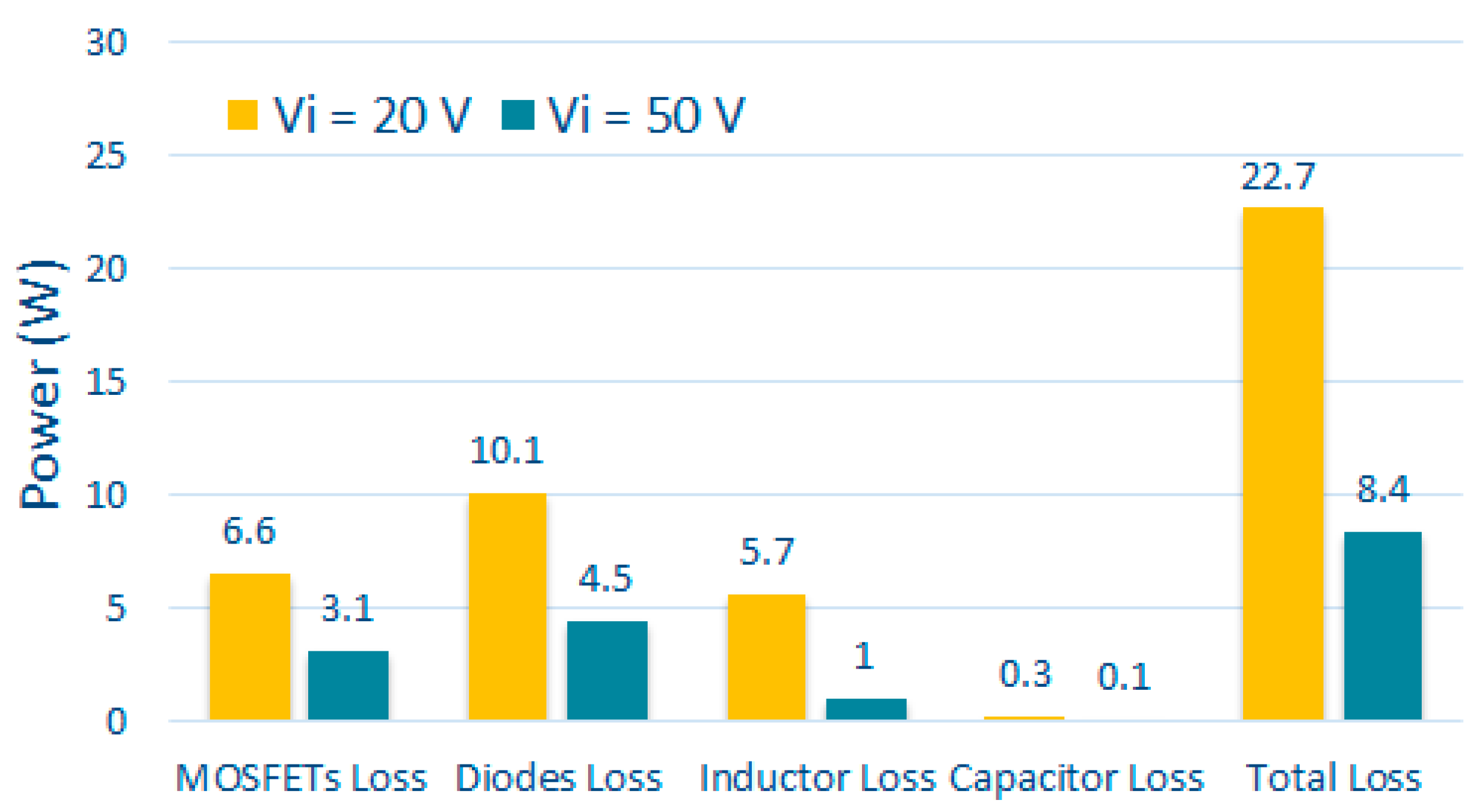
3.4. Power Loss Analysis

In this section, the power loss of the proposed SCQSBC topology is investigated. The power loss calculation can be validated according to conducting time and conducting current of devices, as shown in Table 1. The power loss distribution is included the MOSFETs, diodes, inductor, and capacitors loss. The power loss of MOSFETs can be given:
P M = P C o n _ S 1 + P S w _ S 1 + P C o n _ S 2 + P S w _ S 2 = ( 9 + 20 D + 4 D 2 ) 2 ( 1 2 D ) 2 I o 2 R D S o n + ( 7 2 D ) ( 1 2 D ) 2 V i I o f s ( t o n + t o f f )
where RDSon, fs, ton, and toff are the on-state drain-source resistance, switching frequency, and the turn-on and turn-off times, respectively.
The diode power loss is included the conduction loss and the reverse recovery loss.
P D = P C o n _ D + P S w _ D
The conduction loss of D0, D1, D2 and D3 diodes is calculated as:
P C o n _ D = x = 0 3 P C o n _ D x = ( u D I o + r D I o 2 ) 0.5 + [ u D 4 I o 1 2 D + r D ( 4 I o 1 2 D ) 2 ] 0.5 + [ u D 2 ( 1 + 2 D ) I o 1 2 D + r D ( 2 ( 1 + 2 D ) I o 1 2 D ) 2 ] ( 1 D ) + [ u D 2 I o + r D 4 I o 2 ] 0.5
where uD and rD are the ON-state voltage and the ON-state resistance of diodes, respectively.
The reverse recovery loss of diodes is given:
P S w _ D = x = 0 3 P S w _ D x = 4 Q r r 2 V i 1 2 D f s
where Qrr is the reverse recovery charge of diodes.
Power loss of capacitors can be derived by:
P C = r C 0 i C 0 _ r m s 2 + r C 1 i C 1 _ r m s 2 + r C 2 i C 2 _ r m s 2
The RMS current of C0, C1 and C2 capacitors are derived as:
{ i C 0 _ r m s   = I o 2 ( 0.5 D ) + [ 2 ( 1 + 2 D ) I o 1 2 D ] 2 D + 4 I o 2 0.5 i C 1 _ r m s   = ( I o k C 1 ) 2 D + ( k C k C 1 I o ) 2 ( 1 D ) i C 2 _ r m s   = [ ( k C 2 + 2 D ) I o 2 D ( k C 1 ) ] 2 ( 0.5 D ) + [ ( 2 k C + 4 D 8 k C D + 4 k C D 2 ) I o 2 D ( k C 1 ) ( 1 2 D ) ] 2 D + [ ( 2 k C 2 D ) I o 2 D ( k C 1 ) ] 2 0.5
Power loss of inductor can be given by:
P L = P f e + P c u = k B β f s α A e l e + r L I L _ R M S 2
where B is the AC magnetic flux; fs is the frequency; Ae is the core cross-sectional area; le is the core mean magnetic path length; IL_rms is RMS current of the inductor; and rL is wire resistance. k, α, β can be found from the manufacturer’s datasheet.

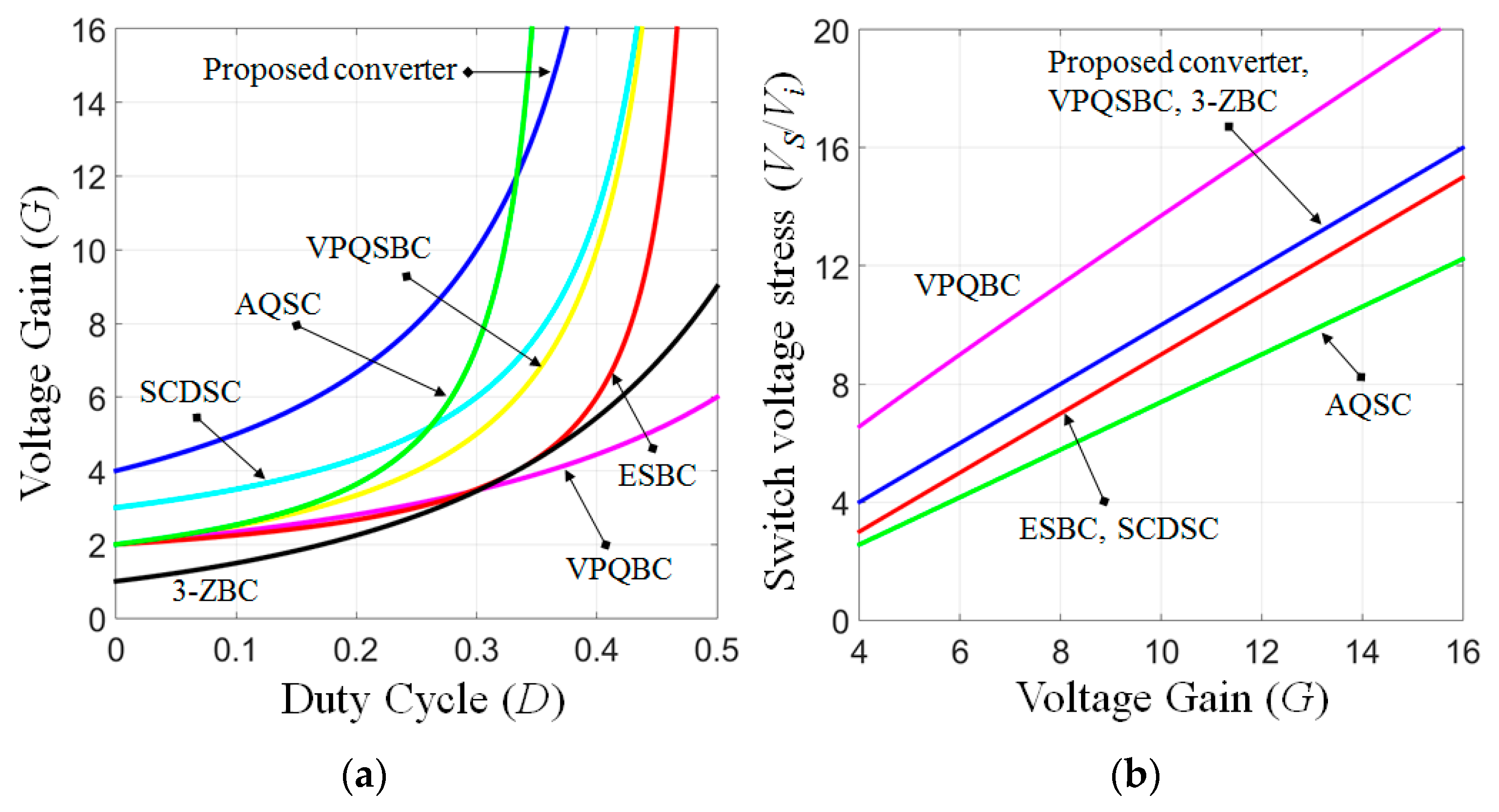
4. Comparison with Other High Gain DC-DC Converter

4.1. Voltage Gain and Count of Device Comparison

In this section, the comparison of the performance of the proposed SCQSBC with other high voltage gain converters is reported. Table 2 presents the comparison count of devices used in these converters. According to Table 2, it can be seen that the proposed SCQSBC has one less inductor than AQSC [21] and VPQBC [24], and two less inductors than 3-ZBC [17]. Moreover, it has two less capacitors than the AQSC [21]. Besides, the total number of devices of the proposed converter has the same with the ESBC [22], SCDSC [23], VPQBC [24], and VPQSBC [24], and less than those of the 3-ZBC [17] and AQSC [21].
The expressions of the voltage gain comparison of the proposed SCQSBC and those of the other high gain converters are shown in Table 2 and also mentioned in Figure 5a. It can be found that the gain of proposed SCQSBC is the highest in compared with other converters through the whole duty cycle lower than 0.33.

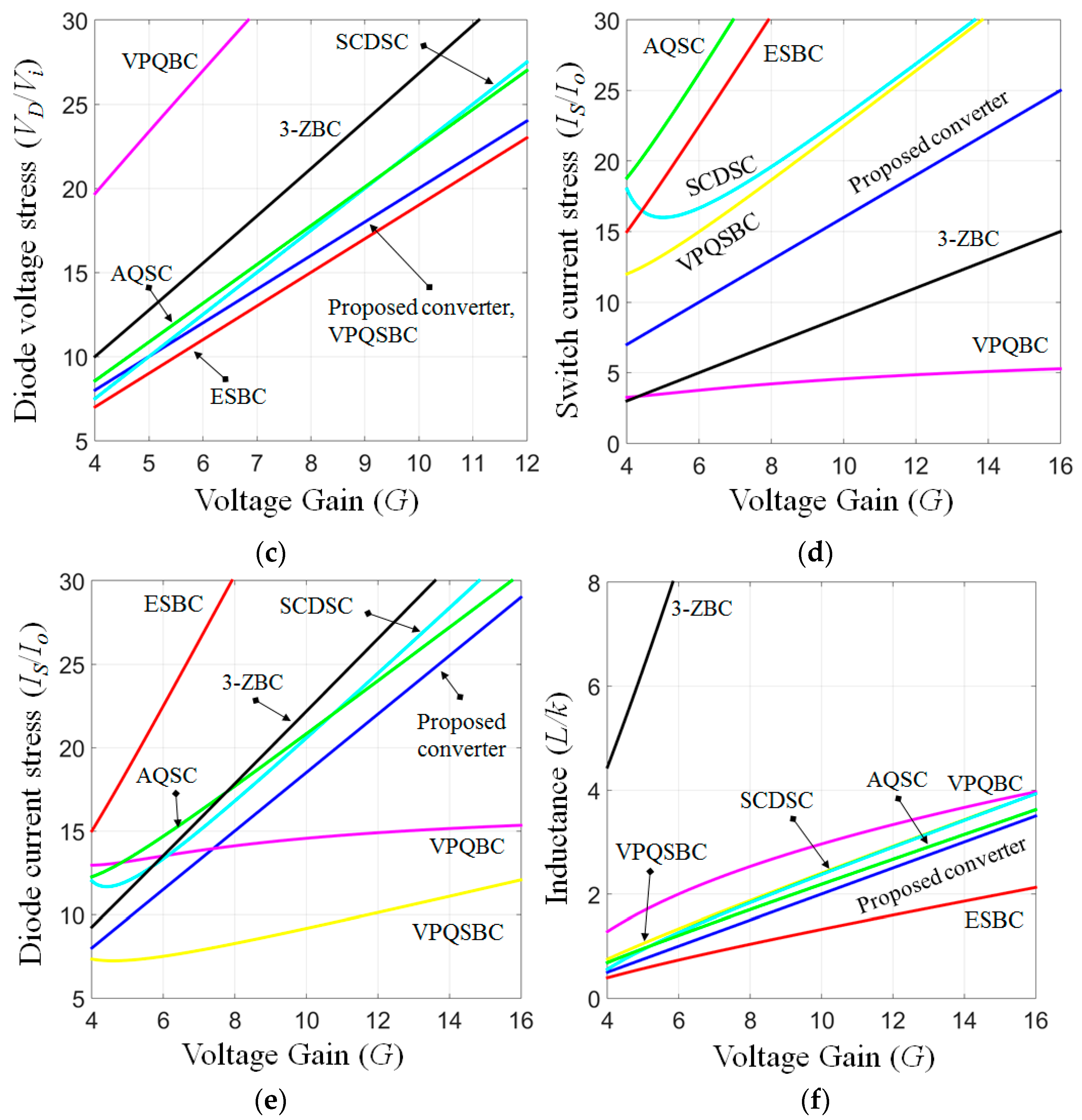
4.2. Voltage and Current Stress Comparison

The detailed voltage and current rating of the proposed SCQSBC and other converters have been shown in Table 2 to make the comparison. It can be seen that the total normalized voltage and current stress of semiconductor devices have been depicted in Figure 5b,c. From Figure 5b, the switch voltage stress of the proposed SCQSBC is the same as those of the VPQSBC [24] and 3-ZBC [17]. Besides this, it is lower than the switch voltage stress of the VPQBC [24] and higher than those of the ESBC [22], SCDSC [23], and AQSC [21]. Moreover, the diode voltage stress of the proposed SCQSBC and VPQSBC is higher than ESBC [22] and lower than those of other converters.
Figure 5d,e depict the plots of the current stress of switches and diode with other converters. It can be seen that the switch current stress of the proposed SCQSBC is lower than that of the AQSC [21], ESBC [22], SCDSC [23], and VPQSBC [24]. However, the SCQSBC has higher switch current stress than that of the 3-ZBC [17] and VPQBC [24]. This is because they only used one switch. In the diode current stress comparison, the diode current stress of VPQSBC is the lowest. Moreover, the SCQSBC is lower than that of the 3-ZBC [17] and AQSC [21]. AQSC [21], ESBC [22], SCDSC [23], and VPQBC [24] in the whole voltage gain from 0 to 7.4.

4.3. Input Current and Inductor Current Ripple Comparison

Based on Table 2, Figure 5f draws the inductance value curves versus output voltage gain among the mentioned converters. It can be noticed that the inductance of the proposed SCQSBC is lower than that of the 3-ZBC, VPQBC, SCDSC, VPQBC, and AQSC. This makes the size of the magnetic element of the proposed SCQSBC small. Note that the inductance comparison was calculated with applying the same operating condition of input voltage, output power, switching frequency, and inductor current ripple. As summarized in Table 2, the input current ripple is considered for comparison. The diode and capacitor are directly connected to the input voltage source in the 3-ZBC, ESBC, and SCDSC, leading to the occurrence of very high input current ripple in these topologies. In the remaining converters, the input current is equal to the inductor current, so it can be observed that the input current ripple of the proposed SCQSBC is the lowest.

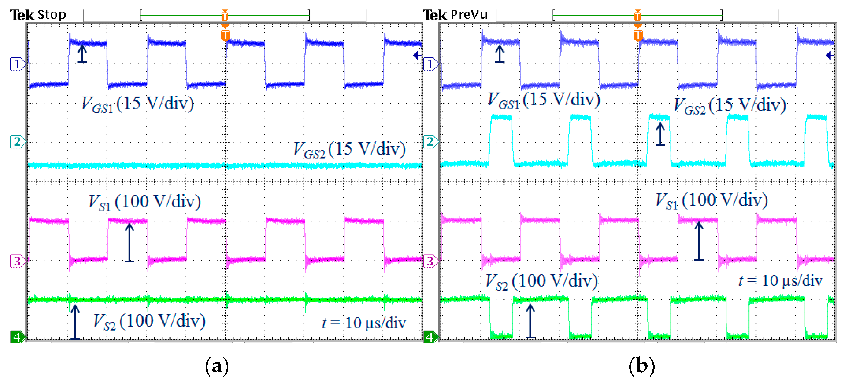
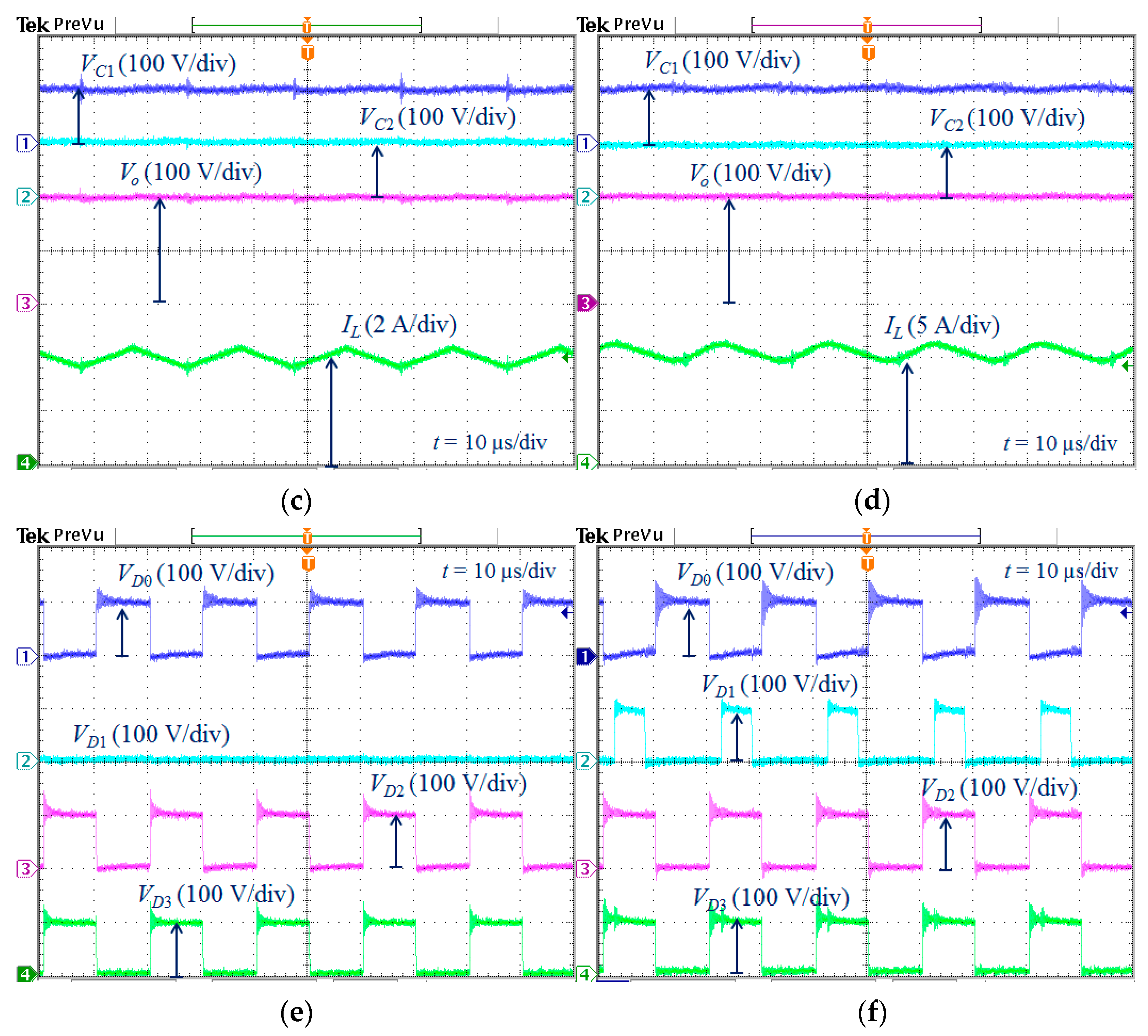
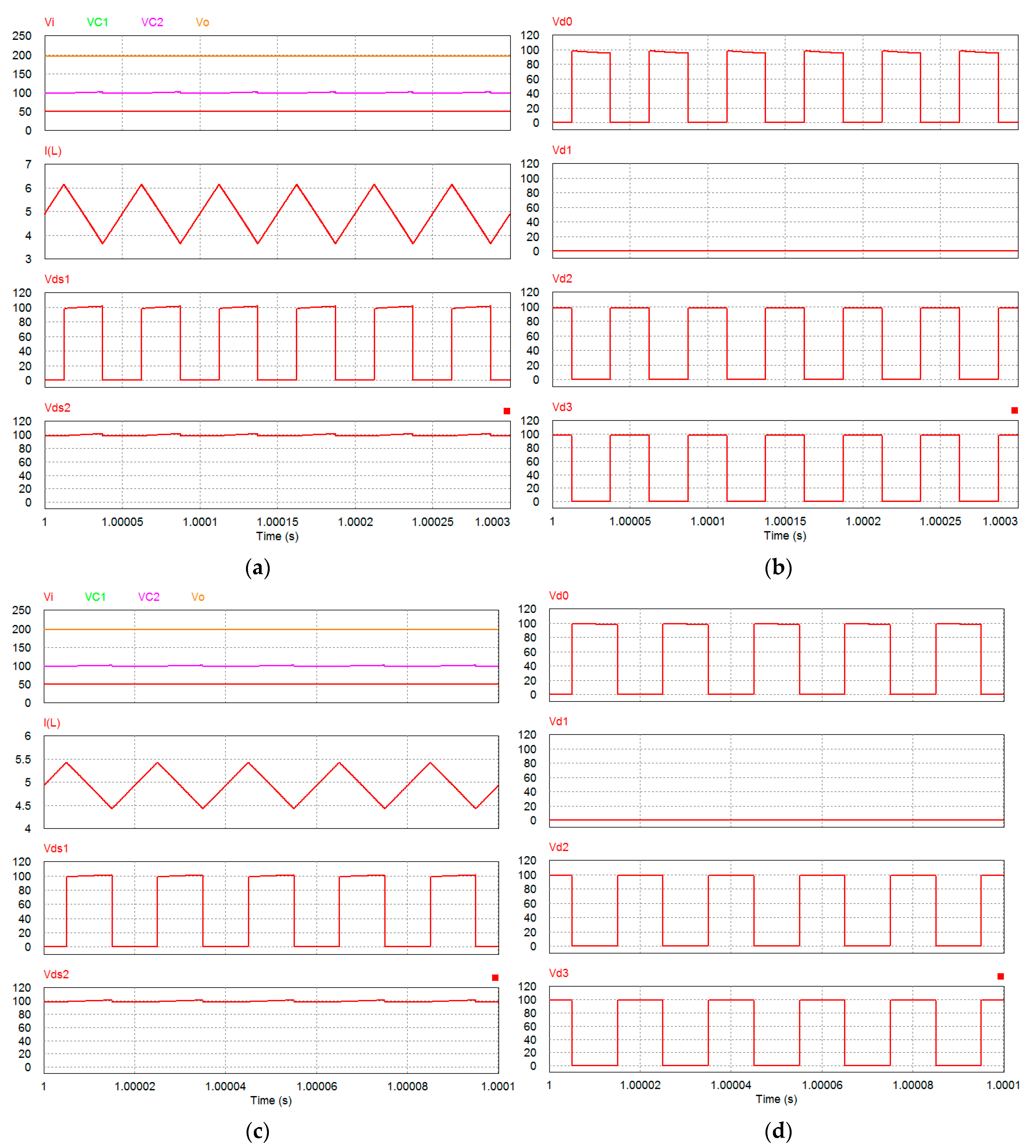
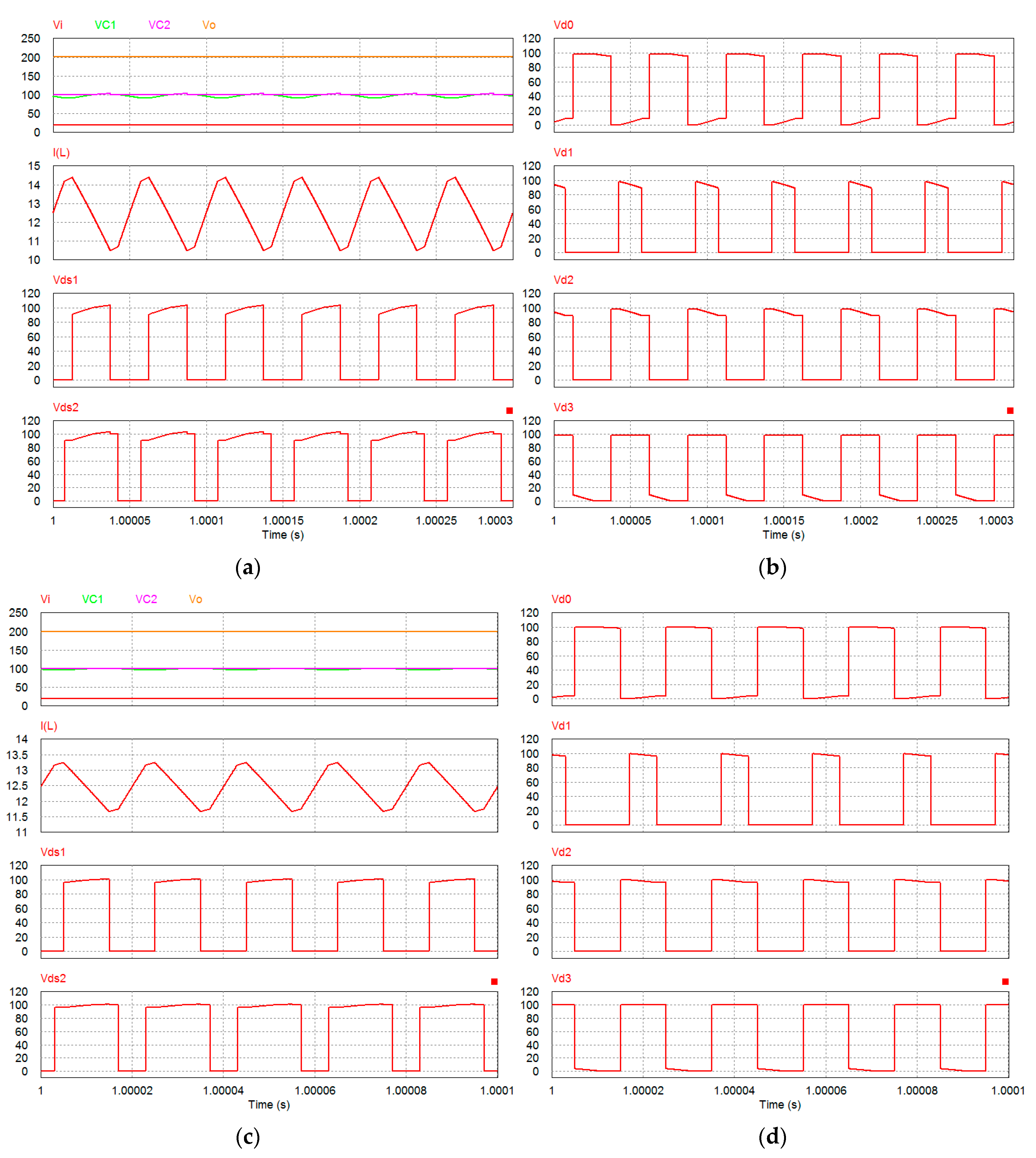
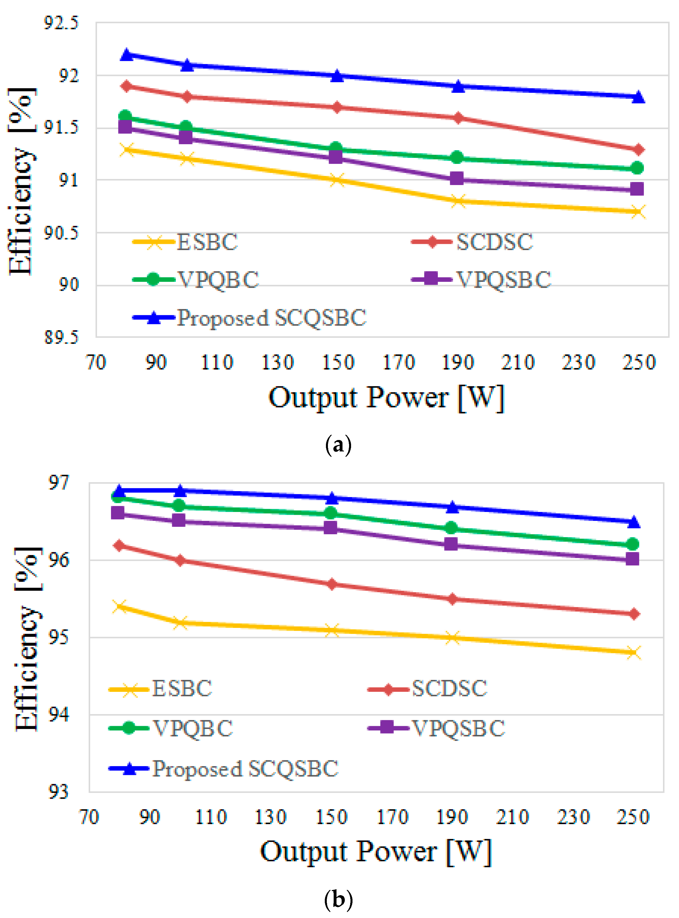
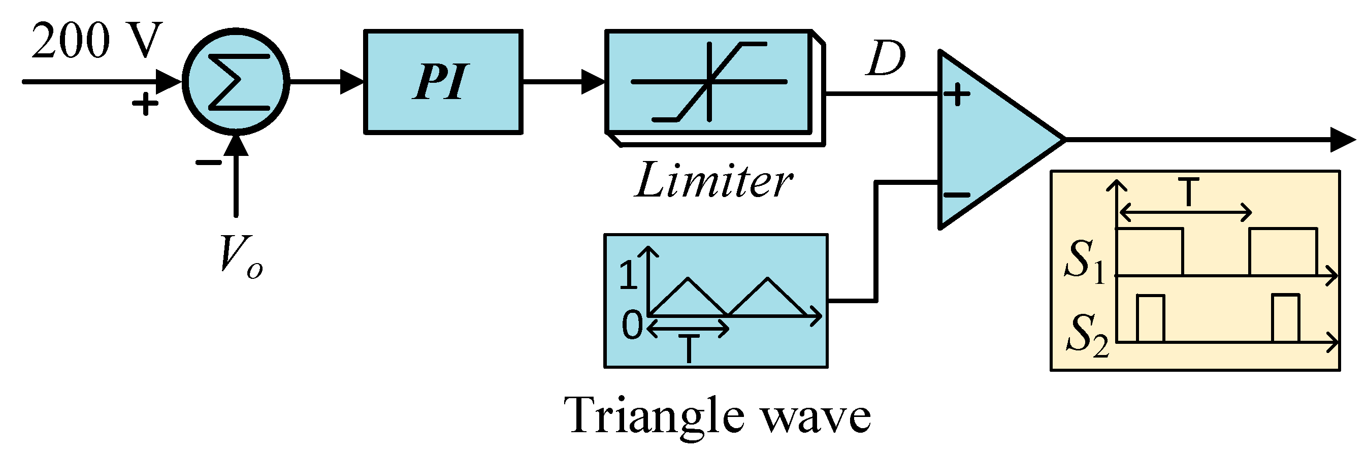
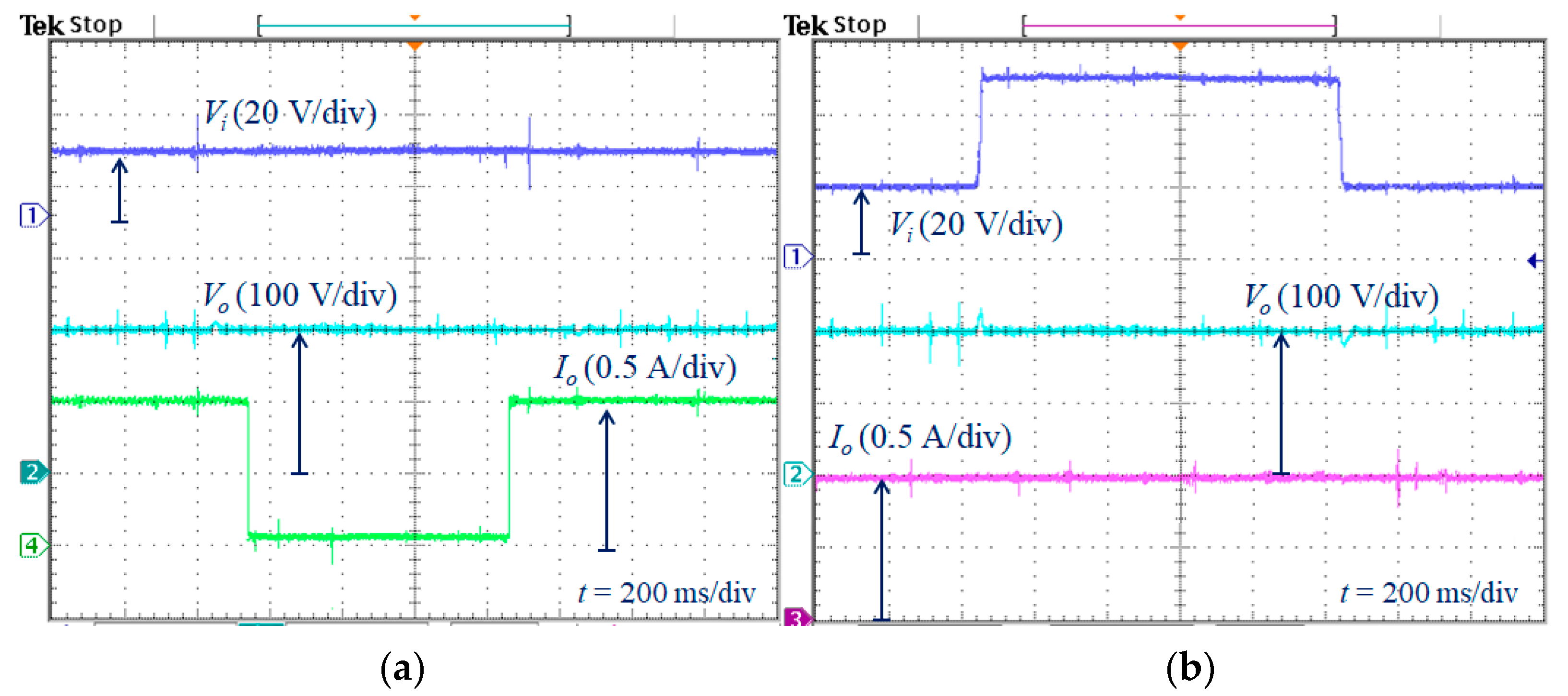
5. Simulation and Experimental Results

In order to verify the precision of the operating capability of SCQSBC, some simulation and experiments have been conducted. For simulation verification, a simulation is built for the SCQSBC parameters are follows: Vi = 20 V (D = 0.3) and Vi = 50 V (D = 0), Vo = 200 V, Po = 250 W, L = 0.5 mH, C1 = C2 = 10 µF, C0 = 110 µF, and all semiconductor devices are ideal. The switching frequencies are 20 kHz and 50 kHz have been tested in the simulation. In two cases, output voltage Vo is 200 V and the voltage stresses across all semiconductor devices and average value of capacitors voltage are half of the output voltage, as shown in Figure 6 and Figure 7. However, the peak-to-peak values of inductor L current and capacitors C1, C2 voltage are increased when the switching frequency is reduced, which are consistent with the calculations obtained in (22) and (24).
The experimental prototype was also designed and shown in Figure 8. The key parameters for the experiment are presented in Table 3. Two power MOSFETs of IRFP4668PbF with low values of rDSon and four Schottky STPS60SM200C diodes were considered to use for the laboratory prototype. The experimental results with the input voltage of 50 V are depicted in Figure 9a,c,e. The obtained waveforms of PWM signals and drain-source of switches S1 and S2 are shown in Figure 9a. The switch S1 has 50% on-state and off-state, while switch S2 is turned off. In this case, the duty cycle D is zero. The average and peak values of the voltage across switch S1 are 52 V and 100 V, respectively. The switch S2 is always off with the peak voltage stress of 100 V. The measured output voltage, capacitor C1, C2 voltage, and input current are 201 V, 100.5 V, 101 V, and 4.3 A, respectively. It can be observed that the input current is continuous with a small ripple, and the peak-to-peak inductor current ripple is 0.85 A. The slope of the input current is magnetizing and demagnetizing due to the on-state of switch S1. The waveform of voltage across the D0, D2 and D3 diodes are reversed-bias with the peak value of 100 V, while the D1 diode is always forward-bias, as depicted in Figure 9e. In another case, the converter has been tested with 20 V DC input voltage and the duty cycle is set 0.3, as shown in Figure 9b,d,f. The PWM control signals for S1 and S2 are also observed and depicted in Figure 9b, where switch S1 is still 50% on-state and off-state. However, switch S2 is turned on with a duty cycle of 0.3. The average and peak values of the voltage rated switch S1 are 52 V and 101 V, respectively. For switch S2, the obtained average and peak values of the voltage across switch S2 are 72 V and 100 V, respectively. It can be obtained that 200.5 V output voltage is produced and the input current is also continuous with the peak-to-peak inductor current ripple of 1.83 A, and the inductor is just demagnetized due to the off-state of switch S1. As depicted in Figure 9f, the voltage stress of the D0, D1, D2, and D3 diodes are 100 V.
Based the analysis in Section 3.4 and the parameters in Table 4, the power loss calculation of the proposed SCQSBC is validated. The power loss distribution is depicted in Figure 10 with the input voltages are 20 V and 50 V. It can be observed that the duty cycle is large when Vi = 20 V leads to decrease the efficiency of the converter. When the input voltage with 50 V is applied, the efficiency is significantly increased. As shown in Figure 10, the power loss of the diode is highest in the loss distribution; this is because the four diodes were used in the proposed SCQSBC. Table 5 shows the measurement current input ripple and peak-to-peak inductor current ripple and efficiency the proposed SCQSBC and other switched-capacitor-based converters in [24]. In this experiment, the input voltage and output power rating are tested in 20 V and 200 W. It can be seen that the peak-to-peak inductor current ripple of the proposed converter is the lowest. Furthermore, the proposed converter can reduce the size of the inductor of the design when compared with other converters. The input current ripple of the proposed converter is also the lowest.
The measured efficiencies of ESBC [22], SCDSC [23], and VPQBC–VPQSBC [24] are highlighted compared with the proposed SCQSBC because they used the same number of components with the proposed SCQSBC. To validate the measured efficiency, the experimental parameters in Table 3 are used for specification of the ESBC [22], SCDSC [23], VPQBC–VPQSBC [24], and the proposed SCQSBC. The plot of measurement efficiency versus output power of the proposed converter and other converters are shown in Figure 11 when the input voltages are 20 V and 50 V. In this case, the output power is measured from 80 W to 250 W. When Vi = 50 V, the proposed SCQSBC achieves the highest efficiency of 97%. When the input voltage is reduced to 20 V, the efficiency of the proposed converter is greater than that of other converters in comparison.
The simple PI controller for output voltage loop has been determined to generate the output voltage is 200 V, as shown in Figure 12. The experimental results are shown under the load transient between light load and full load while input and output voltage are 20 V and 200 V, respectively. Moreover, the input voltage adjustment is also considered from 20 V to 50 V. In this case, the output voltage and power are set at 200 V and 200 W, respectively. As depicted in Figure 13, it can be observed that the output voltage of the proposed SCQSBC is insensitive to the load in Figure 13a or input voltage variation in Figure 13b, and settling time of the converter is approximately 0.1 s.

6. Conclusions

A switched-capacitor-based quasi-switched boost DC-DC converter is presented in this article for low power and high step-up voltage conversion applications. The contributions of the SCQSBC include: providing a high voltage capability with small duty cycle, thereby improving the efficiency of the converter; and a simple topological structure. Moreover, the low input current ripple of the SCQSBC can maintain the lifetime of the power DC sources in renewable energy systems. The theoretical analysis in CCM/DCM boundary condition and parameters design are determined in detail. What is more, the performance comparisons with other transformer-less high gain structures and an experimental verification with single closed-loop controller are provided to demonstrate the characteristics of the proposed SCQSBC. The proposed SCQSBC was suitable for interfacing fuel cells and photovoltaic applications, which required high voltage gain.

Author Contributions

T.-D.D. determined topology, conducted data analysis, and prepared the original draft. M.-K.N. contributed to review and editing. T.-T.T. contributed to validating the simulation and experimental work. Y.-C.L. provided resources and supervision. J.-H.C. provided resources and funding acquisition. All authors have read and agreed to the published version of the manuscript.

Funding

This research received no external funding.

Institutional Review Board Statement

Not applicable.

Informed Consent Statement

Not applicable.

Data Availability Statement

Not applicable.

Acknowledgments

This research was supported by “Regional Innovation Strategy (RIS)” through the National Research Foundation of Korea (NRF) funded by the Ministry of Education (MOE) (2021RIS-002).

Conflicts of Interest

The authors declare no conflict of interest.

References

  1. Loana, M.P.C.; Septimiu, L.; Sorin, P.; Dan, L.; Loan, L.; Radu, M. A New Hybrid Inductor-Based Boost DC-DC Converter Suitable for Applications in Photovoltaic Systems. Energies 2019, 12, 252. [Google Scholar]
  2. Abdulaziz, A.; Khairy, S.; Naif, A.; Ahmed, G.A.K.; Hedra, S. Multi-Port PWM DC-DC Power Converter for Renewable Energy Applications. Energies 2021, 14, 3490. [Google Scholar]
  3. Nguyen, M.K.; Duong, T.D.; Lim, Y.C.; Kim, Y.J. Isolated boost DC-DC converter with three switches. IEEE Trans. Power Electron. 2018, 33, 1389–1398. [Google Scholar]
  4. Bin, G.; Jason, D.; Lai, J.S.; Zheng, Z.; Chuang, L. High boost ratio hybrid transformer DC–DC converter for photovoltaic module applications. IEEE Trans. Power Electron. 2013, 28, 2048–2058. [Google Scholar]
  5. Nguyen, M.K.; Lim, Y.C.; Choi, J.H.; Cho, G.B. Isolated High Step-up DC-DC Converter Based on Quasi-Switched-Boost Network. IEEE Trans. Ind. Electron. 2016, 63, 7553–7562. [Google Scholar] [CrossRef]
  6. Francois, F.; Thiery, A.M.; Eric, L.; Bertrand, G.; Jean, J.H.; Julia, C.B. An isolated multicell intercell transformer converter for applications with a high step-up ratio. IEEE Trans. Power Electron. 2013, 28, 1107–1119. [Google Scholar]
  7. Gang, W.; Xinbo, R.; Zhihong, Y. High step-up DC-DC converter based on switched capacitor and couple inductor. IEEE Trans. Ind. Electron. 2018, 65, 5572–5579. [Google Scholar]
  8. Yam, P.S.; Frede, B.; Poh, C.L. Quasi-Y-source boost DC-DC converter. IEEE Trans. Power Electron. 2015, 30, 6514–6519. [Google Scholar]
  9. Hossein, G.; Reza, S.S.; Mir, R.H.; Ebrahim, A.; Gorji, S.A. Design and Implementation a Single-Switch Step-Up DC-DC Converter Based on Cascaded Boost and Luo Converters. Energies 2021, 14, 3584. [Google Scholar]
  10. Lee, S.W.; Do, H.L. Quadratic Boost DC-DC Converter with High Voltage Gain and Reduced Voltage Stresses. IEEE Trans. Power Electron. 2019, 34, 2397–2404. [Google Scholar] [CrossRef]
  11. Javed, A.; Mohammad, Z.; Adil, S.; Lin, C.H.; Mohammed, A.; Raj, K.Y.; Mohd, T.; Kuntal, S.; Basem, A. A New High-Gain DC-DC Converter with Continuous Input Current for DC Microgrid Applications. Energies 2021, 14, 3629. [Google Scholar]
  12. Ahmad, A.; Pourya, S.; Mehdi, F. Interleaved Multistage Step-Up Topologies with Voltage Multiplier Cells. Energies 2020, 13, 5990. [Google Scholar]
  13. Ebrahim, B.; Hamed, M.M.; Mehran, S.; Seyed, H.H. Extendable Nonisolated High Gain DC-DC Converter Based on Active–Passive Inductor Cells. IEEE Trans. Ind. Electron. 2018, 65, 9478–9487. [Google Scholar]
  14. Sajad, R.; Vahid, A.; Frede, B. Implementation of a common grounded Z-source dc-dc converter with improved operation factors. IET Power Electron. 2019, 12, 2245–2255. [Google Scholar]
  15. Veda, P.G.; Marian, K.K. Analysis of PWM Z-source dc-dc converter in CCM for steady state. IEEE Trans. Circuits Syst. I Reg. Pap. 2012, 59, 854–863. [Google Scholar]
  16. Punit, K.; Mummadi, V. Z-network plus switched-capacitor boost dc-dc converters. IEEE J. Emerg. Sel. Top. Power Electron. 2021, 9, 791–803. [Google Scholar]
  17. Guidong, Z.; Bo, Z.; Zhong, L.; Dongyuan, Q.; Liqiang, Y.; Wolfgang, A.H. A 3-Z-network boost converter. IEEE Trans. Ind. Electron. 2015, 62, 278–288. [Google Scholar]
  18. Santanu, M.; Ravindranath, A.; Avinash, J. Inverse Watkins-Johnson topology based inverter. IEEE Trans. Power Electron. 2012, 27, 1066–1070. [Google Scholar]
  19. Nguyen, M.K.; Le, T.V.; Park, S.J.; Lim, Y.C. A class of quasi-switched boost inverters. IEEE Trans. Ind. Electron. 2015, 62, 1526–1536. [Google Scholar] [CrossRef]
  20. Alencar, F.D.S.; Fernanđo, L.T.; Enio, R.R. Switched Capacitor DC-DC Converters: A Survey on the Main Topologies, Design Characteristics, and Applications. Energies 2021, 14, 2231. [Google Scholar]
  21. Xiaoquan, Z.; Bo, Z.; Ke, J. Hybrid nonisolated active quasi-switched DC-DC converter for high step-up voltage conversion applications. IEEE Access 2020, 8, 222584–222598. [Google Scholar]
  22. Xiaoquan, Z.; Bo, Z.; Zhong, L.; Hong, L.; Li, R. Extended switched-boost DC-DC converters adopting switched-capacitor cells for high step-up conversion. IEEE J. Emerg. Sel. Topics Power Electron. 2017, 5, 1020–1030. [Google Scholar]
  23. Nguyen, M.K.; Duong, T.D.; Lim, L.C. Switched-capacitor-based dual-switch high-boost dc-dc converter. IEEE Trans. Power Electron. 2018, 33, 4181–4189. [Google Scholar] [CrossRef]
  24. Guidong, Z.; Zhiyang, W.; Samson, S.Y.; Si, Z.C.; Bo, Z.; Herbert, H.C.I.; Yun, Z. A generalized additional voltage pumping solution (GAVPS) for high-step-up converters. IEEE Trans. Power Electron. 2019, 34, 6456–6467. [Google Scholar]
Figure 1. Proposed SCQSB converter.
Energies 14 06591 g001
Figure 2. Typical waveform of proposed SCQSBC for (a) CCM and (b) DCM.
Energies 14 06591 g002
Figure 3. Operating modes of proposed SCQSBC: (a) Mode I, (b) Mode II, (c) Mode III, and (d) Mode IV (DCM).
Energies 14 06591 g003aEnergies 14 06591 g003b
Figure 4. CCM/DCM boundary condition of the SCQSBC.
Energies 14 06591 g004
Figure 5. Comparison between the proposed converter and other converters: (a) Voltage gains versus duty cycle, (b) Total voltage rating of switches, (c) Total voltage rating of diodes, (d) Total current rating of switches, (e) Total current rating of diodes, and (f) Inductance.
Energies 14 06591 g005aEnergies 14 06591 g005b
Figure 6. Simulation results with Vi = 50 V: (a,b) fs = 20 kHz and (c,d) fs = 50 kHz. From top to bottom: input voltage, output voltage, capacitors C1, C2 voltage; inductor current; the drain-source of switch S1 and S2; diodes D0, D1, D2 and D3 voltage stress.
Energies 14 06591 g006
Figure 7. Simulation results with Vi = 20 V: (a,b) fs = 20 kHz and (c,d) fs = 50 kHz. From top to bottom: input voltage, output voltage, capacitors C1, C2 voltage; inductor current; the drain-source of switch S1 and S2; diodes D0, D1, D2 and D3 voltage stress.
Energies 14 06591 g007
Figure 8. Prototype of proposed SCQSBC.
Energies 14 06591 g008
Figure 9. Experimental results with Vi = 50 V (left side) and 20 V (right side). (a,b) Bottom to top: The drain-source and gate-source voltage of switch S1 and S2; (c,d) output voltage, capacitors C1, C2 voltage, inductor current; (e,f) diode D3, D2, D1 and D0 voltage stress.
Energies 14 06591 g009aEnergies 14 06591 g009b
Figure 10. Power loss distribution.
Energies 14 06591 g010
Figure 11. Measured efficiency comparison at (a) Vi = 20 V, and (b) Vi = 50 V.
Energies 14 06591 g011
Figure 12. Simple PI controller for the proposed SCQSBC.
Energies 14 06591 g012
Figure 13. Experimental results with closed-loop control. (a) The load change and (b) Input voltage change.
Energies 14 06591 g013
Table 1. Conducting current and period of devices.
ComponentsConducting CurrentConducting Period
S1 3 2 D 1 2 D I o 0.5 × T
S2 4 1 2 D I o D × T
D0Io0.5 × T
D1 4 1 2 D I o (1 − D) × T
D2 2 ( 1 + 2 D ) 1 2 D 0.5 × T
D32Io0.5 × T
L 4 1 2 D I o T
C1 I o k C 1 D × T
k C k C 1 I o (1 − D) × T
C2 k C 2 + 2 D 2 D ( k C 1 ) I o (0.5 − D) × T
2 k C + 4 D 8 k C D + 4 k C D 2 2 ( k C 1 ) D ( 1 2 D ) I o D × T
2 k C 2 D 2 D ( k C 1 ) I o 0.5 × T
CoIo(0.5 − D) × T
2 ( 1 + 2 D ) 1 2 D I o D × T
2Io0.5 × T
Table 2. Comparison of the proposed SCQSBC topology with considered topologies.
3-ZBC [17]AQSC [21]ESBC [22]SCDSC [23]VPQBC [24]VP-QSBC [24]Proposed SCQSBC
Inductor/Capacitor4/22/41/31/32/31/31/3
Switch/Diode1/92/42/42/41/42/42/4
Total of Devices16121010101010
Voltage gain ( 1 + D 1 D ) 2 2 ( 1 D ) 1 3 D + D 2 2 ( 1 D ) 1 2 D 3 2 D 1 2 D 2 D ( 1 D ) 2 2 1 2 D 4 1 2 D
Normalized capacitor voltage stress (VC/Vi) 1 + D 1 D
( 1 + D 1 D ) 2
D 1 3 D + D 2
1 D 1 3 D + D 2
2 ( 1 D ) 1 3 D + D 2
D 1 2 D
1 D 1 2 D
2 ( 1 D ) 1 2 D
1 1 2 D
3 2 D 1 2 D
1 1 D
1 ( 1 D ) 2
2 D ( 1 D ) 2
1 1 2 D
2 1 2 D
2 1 2 D
4 1 2 D
Normalized switch voltage stress (VS/Vi) ( 1 + D 1 D ) 2 D 1 3 D + D 2
1 D 1 3 D + D 2
D 1 2 D
1 D 1 2 D
1 1 2 D 1 ( 1 D ) 2 1 1 2 D 2 1 2 D
Normalized diode voltage stress (VD/Vi)D/(1 − D)
1
2D(1 + D)/(1 − D)2
(1 + D)/(1 − D)
D(1 + D)/(1 − D)2
(1 + D)2/(1 − D)2
1 1 3 D + D 2
1 D 1 3 D + D 2
1 D 1 2 D
D 1 2 D
2 1 2 D
1 1 2 D
1 ( 1 D ) 2
1 1 D
D ( 1 D ) 2
1 1 2 D 2 1 2 D
Switch current stress (IS/Io) 4 D ( 1 D ) 2 2 1 3 D + D 2
1 + D D 2 D ( 1 3 D + D 2 )
2 1 2 D
1 D ( 1 2 D )
1 D ( 1 2 D ) 1 + D D 2 D ( 1 D ) 2 2 1 2 D
1 D ( 1 2 D )
3 2 D 1 2 D
4 1 2 D
Diode current stress (ID/Io)D(1 + D)/(1 − D)2
(1 + D)/(1 − D)
2D(1 + D)/(1 − D)2
D/(1 − D)
1
1/D
2 1 3 D + D 2
1 1 D
1/D
1 1 3 D + 2 D 2
1 1 D
2 1 2 D
1/D
1 1 D
2 1 2 D
1 ( 1 D ) ( 1 2 D )
1/D
2 D ( 1 D ) 2
1 1 D
1/D
D ( 1 D ) ( 1 2 D )
1 1 D
1
4 1 2 D
2 ( 1 + 2 D ) 1 2 D
2
Inductances D ( 1 + D ) k L
D ( 1 + D ) 3 ( 1 D ) 2 k L
2 D ( 1 D ) 2 1 3 D + D 2 k L D ( 1 D ) 2 1 2 D k L D ( 1 D ) ( 3 2 D ) 1 2 D k L D ( 2 D ) 1 D k L
D k L
2 D ( 1 D ) 1 2 D k L 1 + 2 D 2 ( 1 2 D ) k L
Input current rippleHighLowHighHighLowLowVery low
kL is coefficient of inductor.
Table 3. Experimental parameters.
ParameterValues
Input voltage range20 V to 50 V
Output voltage200 V
Power rating250 W
Inductor (L)0.5 mH
Capacitors10 µF/160 V for C1, C2
110 µF/450 V for C0
Switching frequency50 kHz
MOSFETsIRFP4668PbF
DiodesSTPS60SM200C
Table 4. Parameters for power loss analysis.
ParametersValues
InductorCoreCM777125 (142 nH/N2)
Copper-wire0.04 Ω
CapacitorsC1, C23.2 mΩ
Co4 mΩ
Power switchesIRFP4668PbF (200 V, 130 A, RDSon = 8 mΩ)
Power diodesSTPS60SM200C (200V, 30A, UD = 0.7 V)
Table 5. Input current ripple and efficiency of VPQBC, VPQSBC, and proposed SCQSBC at Vi = 20 V and Po = 250 W.
ConverterVPQBCVPQSBCProposed SCQSBC
ΔIin1.3 A1.2 A0.8 A
Efficiency91.1%90.9%91.8%
Publisher’s Note: MDPI stays neutral with regard to jurisdictional claims in published maps and institutional affiliations.

