
Discontinuous Current Mode Modeling and Zero Current Switching of Flyback Converter

 ,
, 
Abstract
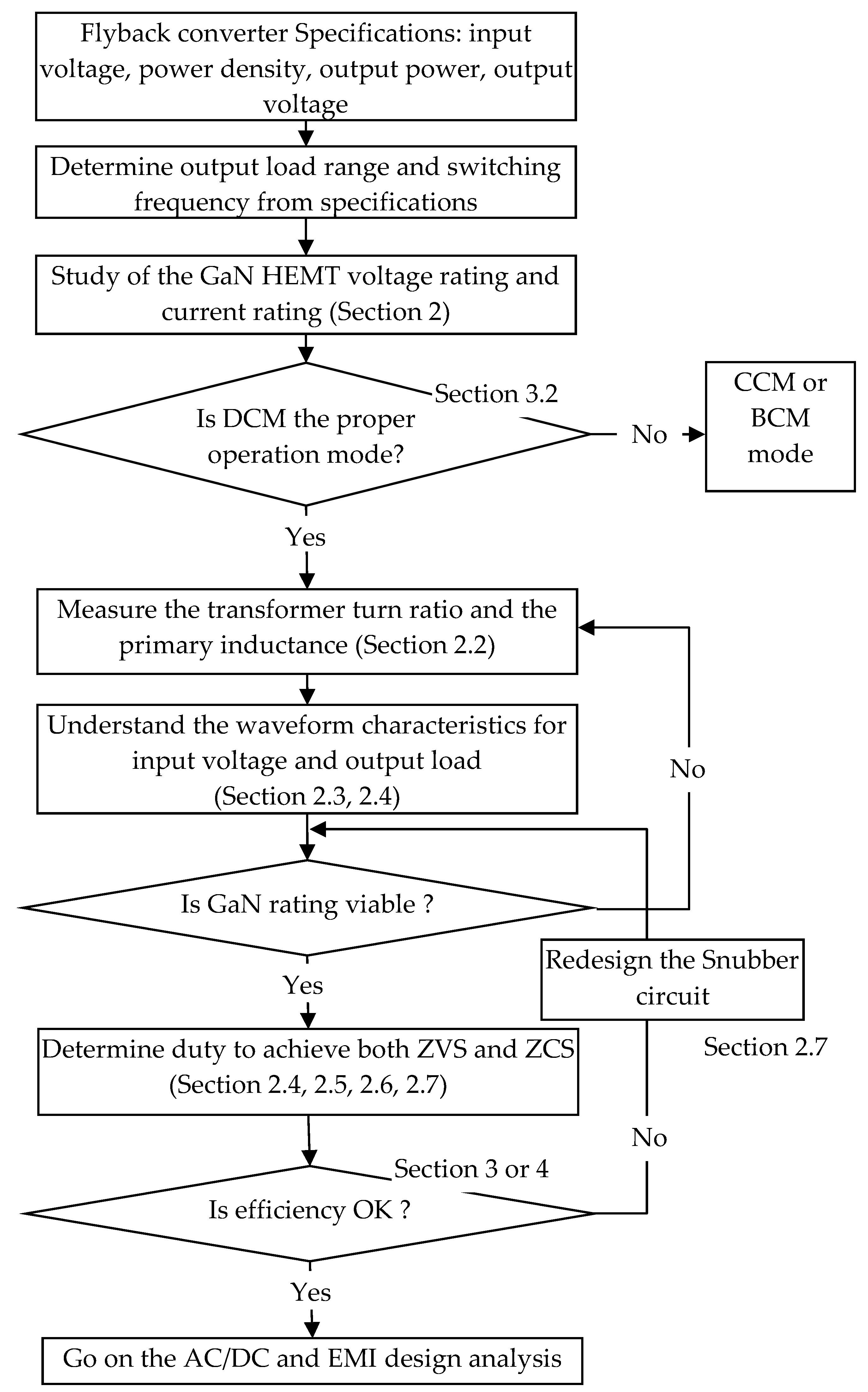
:1. Introduction
2. Materials and Methods
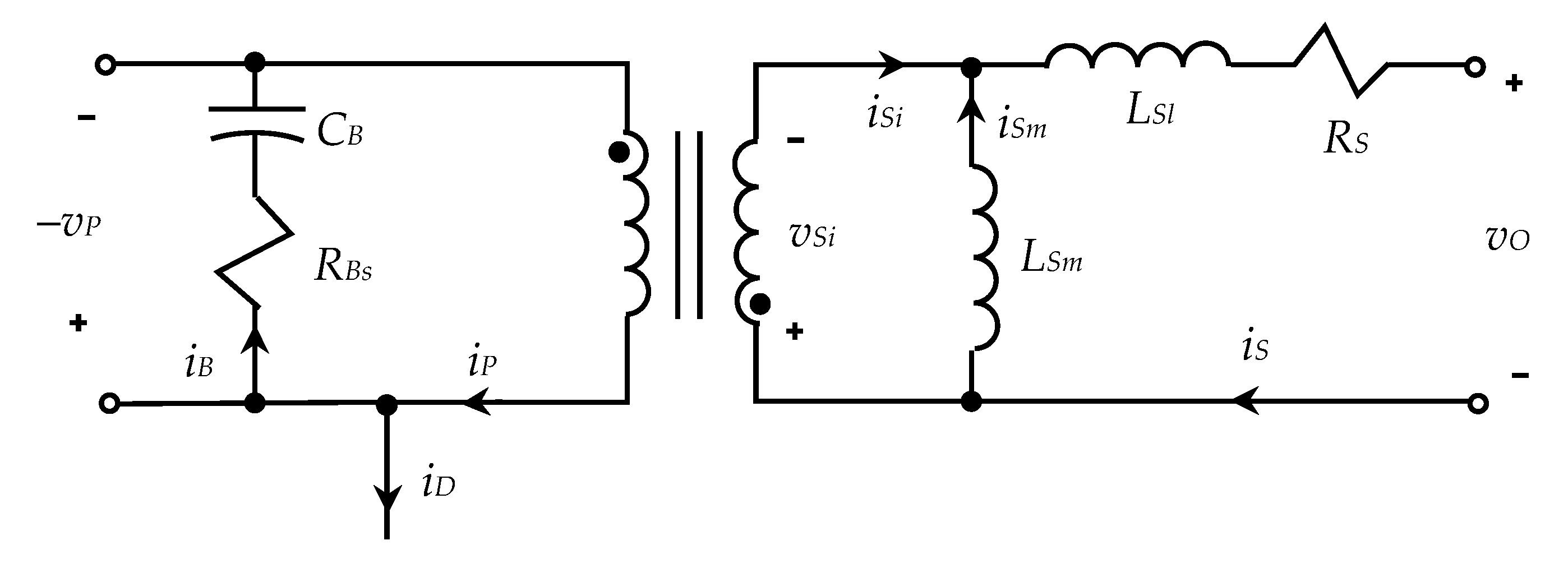
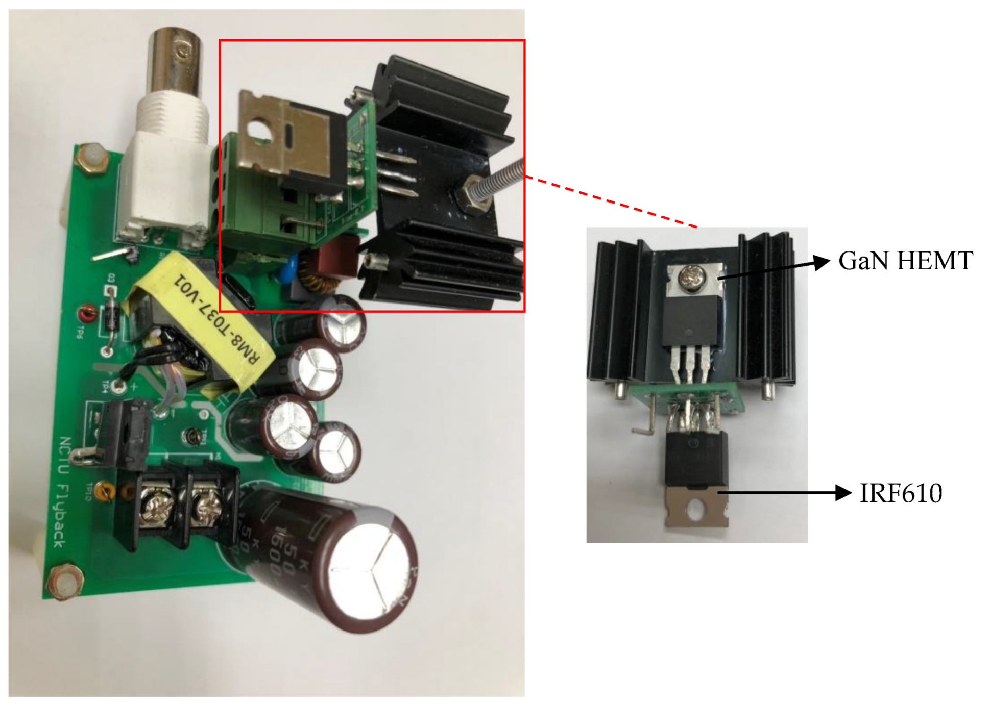
2.1. Flyback Converter Circuit
2.2. Transformer
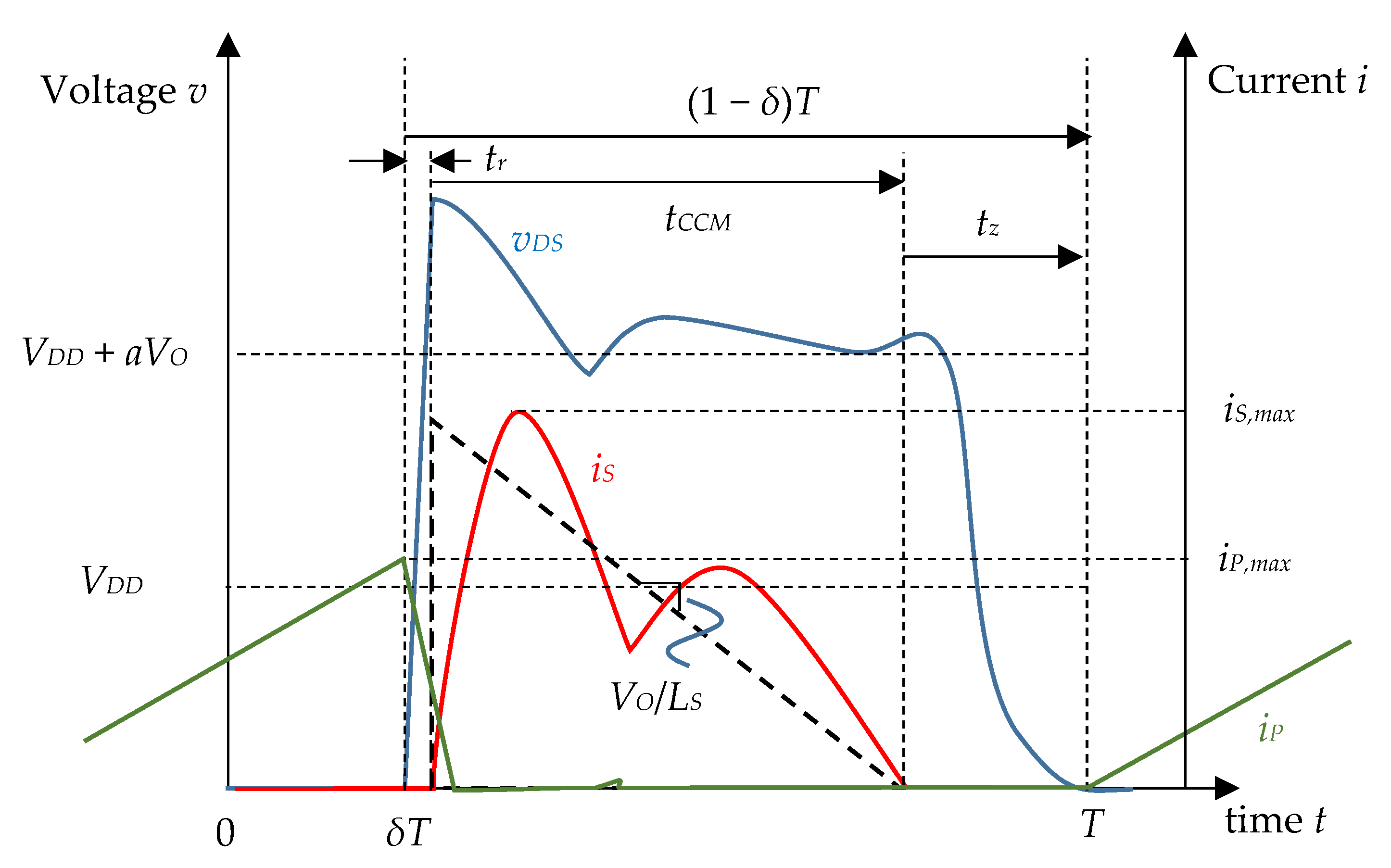
2.3. Wave Form Assumptions
- (1)
- the drain-source voltage rising phase,
- (2)
- the current flowing on the secondary winding phase, and,
- (3)
- the zero current in the secondary winding phase.
2.4. Steady State Assumptions
- (1)
- The ratio of the peak value of currents is:where denotes the transformer peak current attenuation. It shall be noted that the attenuation does not imply the energy loss; however, it has the effect to the current flowing time on the secondary winding.
- (2)
- Current flows in the secondary winding only during the diode conduction time which is referred to as the continuous current time tCC. This assumption can be written into two equations separately as follows.
2.5. Drain-Source Voltage Rising Phase
2.6. Current Flowing on the Secondary Winding Phase
2.7. Zero Current in the Secondary Winding Phase and Zero Current Switching
3. Analysis
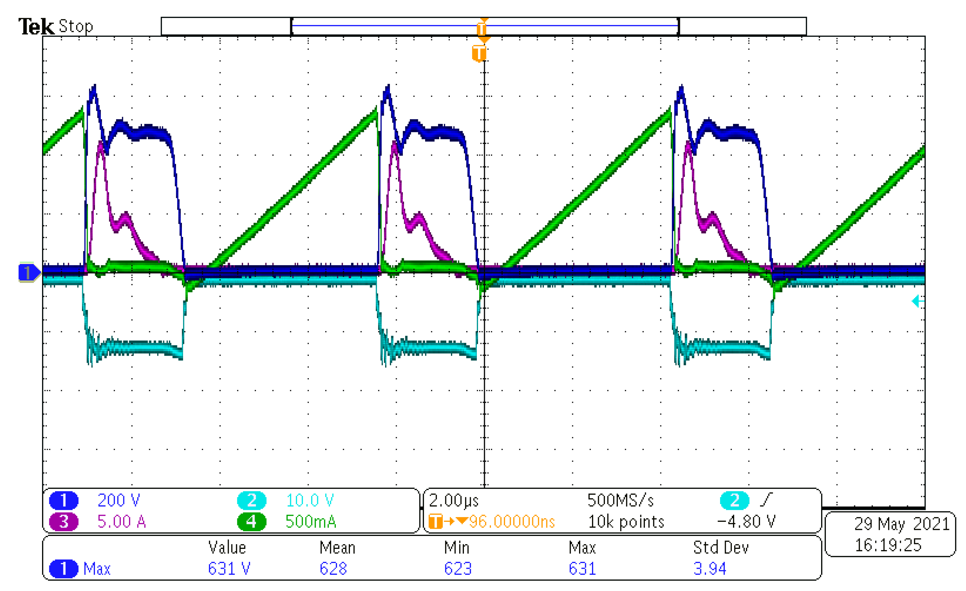
3.1. SPICE Simulation Analysis
3.2. Critical Condition for DCM
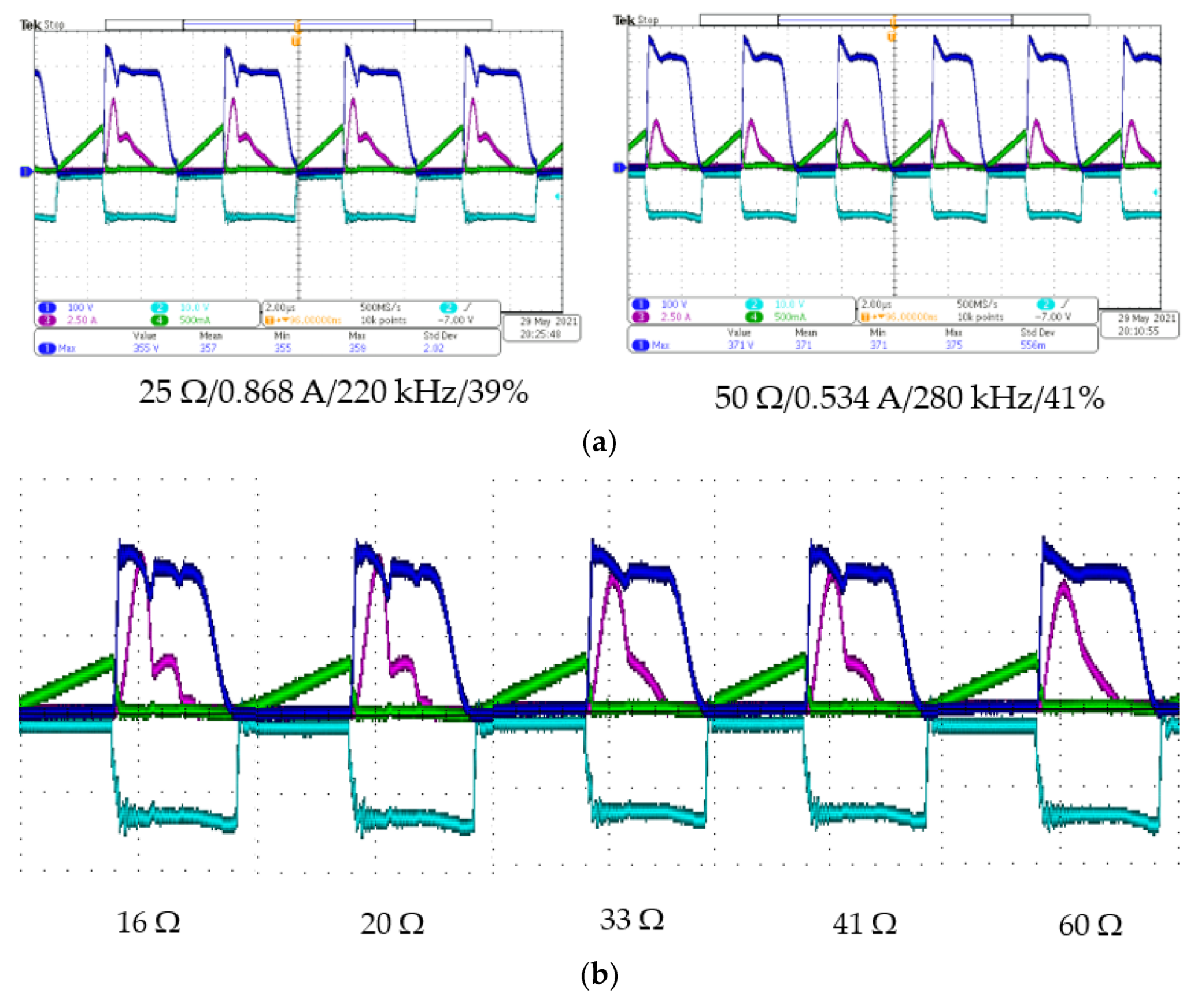
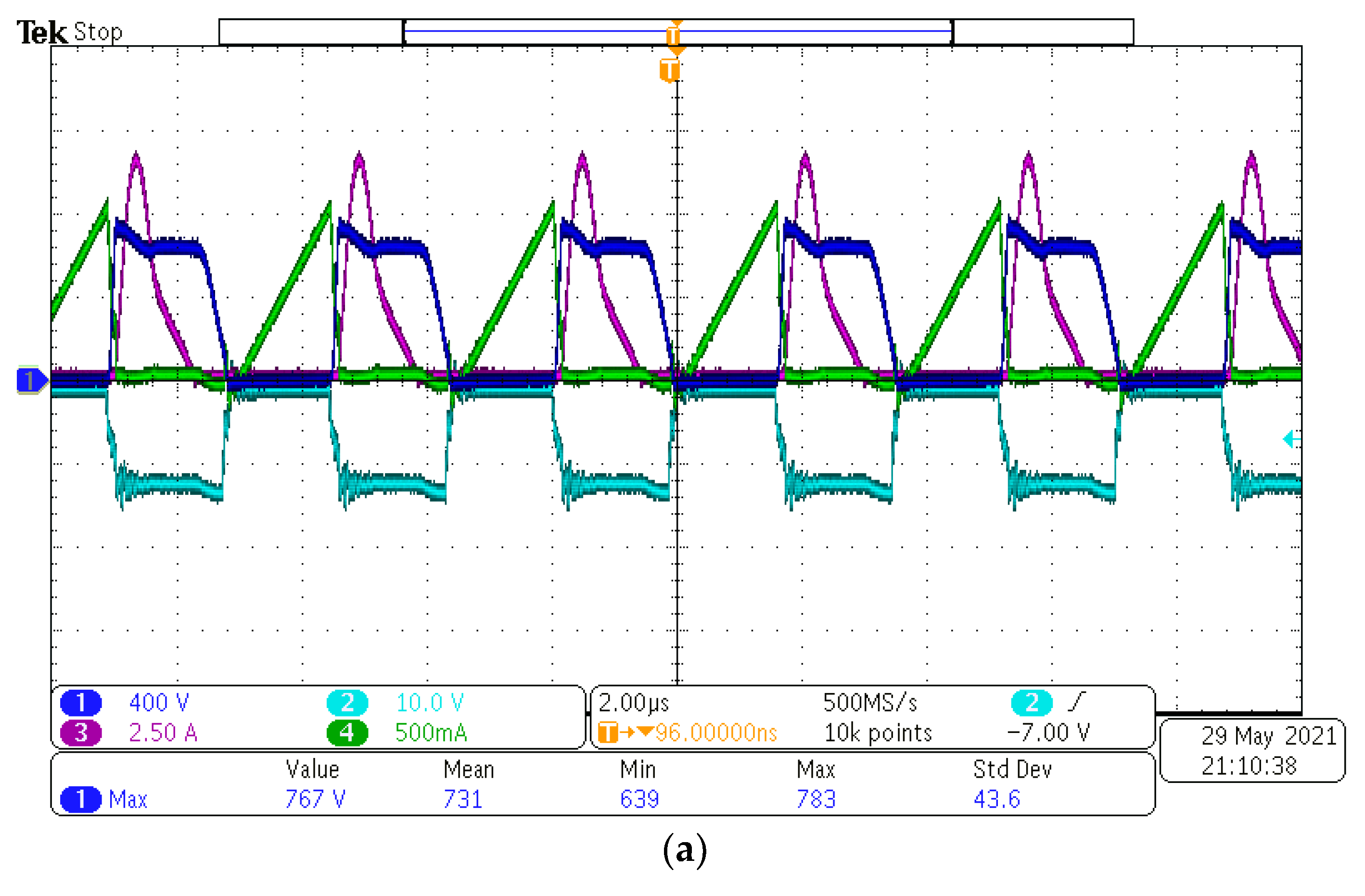
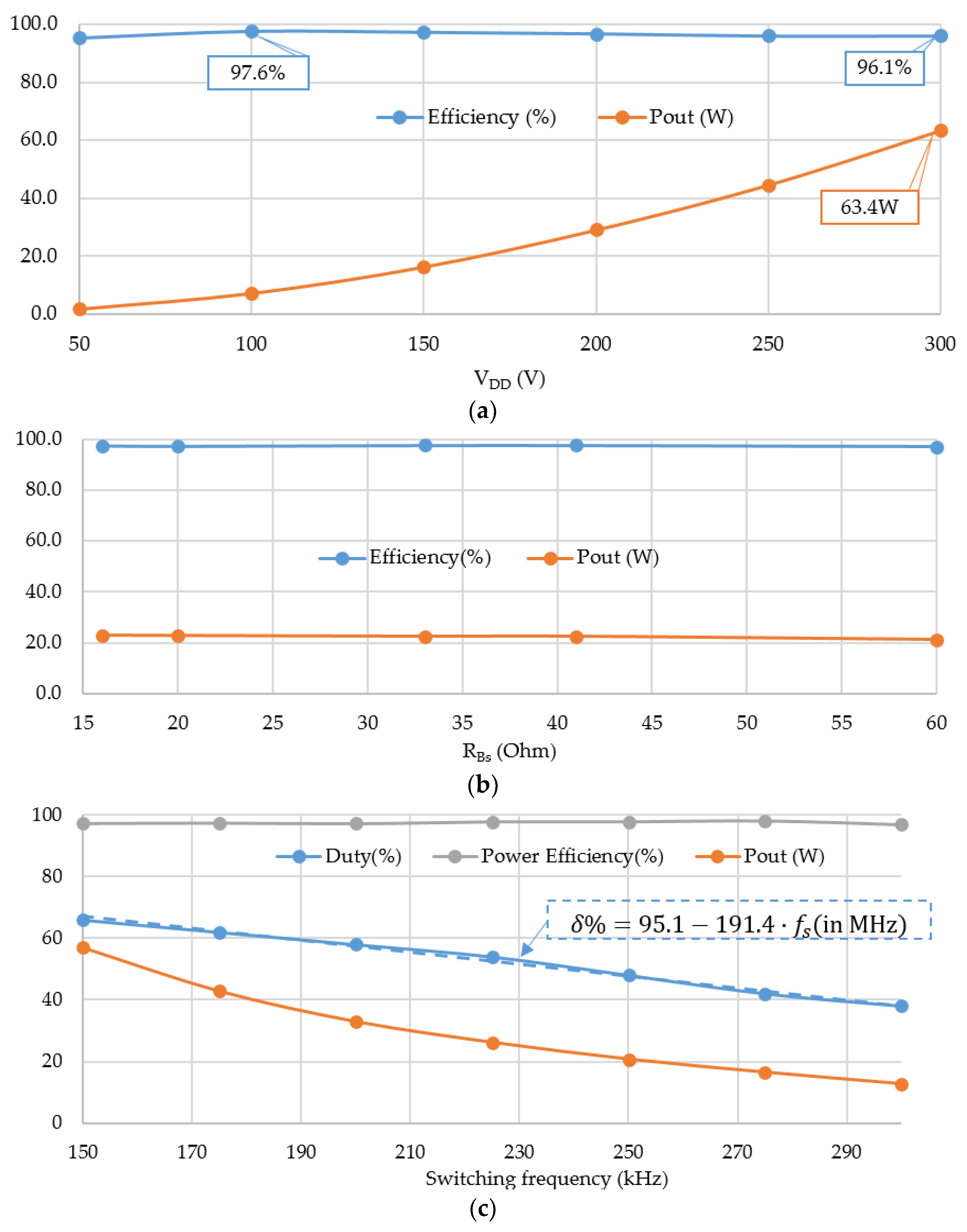
4. Results and Comparisons
5. Analysis and Discussion
6. Conclusions
Author Contributions
Funding
Institutional Review Board Statement
Informed Consent Statement
Data Availability Statement
Acknowledgments
Conflicts of Interest
Nomenclature
| Symbol | Abbreviation |
| LP | inductance of primary winding |
| LPm | magnetization inductance of primary winding |
| LPl | leakage inductance of primary winding |
| LS | inductance of secondary winding |
| LSl | leakage inductance of secondary winding |
| k | coupling coefficient of transformer |
| a | turn ratio of transformer |
| Cm | coupling capacitance of transformer |
| CDS | drain-source parasitic capacitance of the switch |
| Coss | output parasitic capacitance of the switch |
| vDS | drain-source voltage of the switch |
| CB | snubber capacitance |
| tCCM | continuous current mode time |
| DS | diode on secondary winding |
| DB | diode of the snubber |
| δ | duty cycle of the switching |
| ω | natural frequency of response |
| damping ratio of response | |
| CO | output capacitance |
| RO | output resistance |
References
- Ahmad, A.; Alam, M.S.; Chabaan, R. A Comprehensive Review of Wireless Charging Technologies for Electric Vehicles. IEEE Trans. Transp. Electrif. 2018, 4, 38–63. [Google Scholar] [CrossRef]
- Liu, C.-Y.; Wang, G.-B.; Wu, C.-C.; Chang, E.Y.; Cheng, S.; Chieng, W.-H. Derivation of the Resonance Mechanism for Wireless Power Transfer Using Class-E Amplifier. Energies 2021, 14, 632. [Google Scholar] [CrossRef]
- Bhattacharya, T.; Giri, V.; Mathew, K.; Umanand, L. Multiphase Bidirectional Flyback Converter Topology for Hybrid Electric Vehicles. IEEE Trans. Ind. Electron. 2008, 56, 78–84. [Google Scholar] [CrossRef]
- Tahan, M.; Bamgboje, D.O.; Hu, T. Compensated Single Input Multiple Output Flyback Converter. Energies 2021, 14, 3009. [Google Scholar] [CrossRef]
- Vairavasundaram, I.; Varadarajan, V.; Pavankumar, P.J.; Kanagavel, R.K.; Ravi, L.; Vairavasundaram, S. A Review on Small Power Rating PV Inverter Topologies and Smart PV Inverters. Electronics 2021, 10, 1296. [Google Scholar] [CrossRef]
- Kumar, R.; Behera, R.K. A Low Cost Distributed Solar DC Nanogrid: Design and Deployment with Remote Monitoring Unit. In Proceedings of the 2018 20th National Power Systems Conference (NPSC), Tiruchirappalli, India, 14–16 December 2018; pp. 1–6. [Google Scholar] [CrossRef]
- Grau, A.; Indri, M.; Bello, L.L.; Sauter, T. Industrial robotics in factory automation: From the early stage to the Internet of Things. In Proceedings of the IECON 2017—43rd Annual Conference of the IEEE Industrial Electronics Society, Beijing, China, 29 October–1 November 2017; pp. 6159–6164. [Google Scholar] [CrossRef] [Green Version]
- Li, M.; Ouyang, Z.; Andersen, M.A.E. Analysis and Optimal Design of High-Frequency and High-Efficiency Asymmetrical Half-Bridge Flyback Converters. IEEE Trans. Ind. Electron. 2020, 67, 8312–8321. [Google Scholar] [CrossRef]
- Murthy, D.; Kazimierczuk, M.K. Performance evaluation of flyback converter. In Proceedings of the Proceedings Electrical Insulation Conference and Electrical Manufacturing Expo, 2005, Indianapolis, IN, USA, 23–26 October 2005; pp. 408–416. [Google Scholar] [CrossRef]
- Fagnani, A. Isolated Continuous Conduction Mode Flyback Using the TPS55340; Application Report slva559; Texas Instruments: Dallas, TX, USA, 2013; Available online: https://www.ti.com/lit/an/slva559/slva559.pdf (accessed on 31 December 2012).
- Lin, B.R.; Chiang, H.K.; Chen, K.C.; Wang, D. Analysis, design and implementation of an active clamp flyback converter. In Proceedings of the 2005 International Conference on Power Electronics and Drives Systems, Kuala Lumpur, Malaysia, 28 November–1 December 2005; pp. 424–429. [Google Scholar] [CrossRef]
- Watson, R.; Lee, F.C.; Hua, G.C. Utilization of an active-clamp circuit to achieve soft switching in flyback converters. IEEE Trans. Power Electron. 1996, 11, 162–169. [Google Scholar] [CrossRef]
- Wong, J.-S.; Wang, H.-C.; Lin, C.-W.; Xu, H.-Y.; Su, Y.-Y.; Wang, J.-M. Analysis of an Active-Clamp Flyback Converter. In Proceedings of the 2020 IEEE International Conference on Consumer Electronics-Taiwan (ICCE-Taiwan), Taoyuan, Taiwan, 28–30 September 2020; pp. 1–2. [Google Scholar] [CrossRef]
- Spiazzi, G.; Mattavelli, P.; Costabeber, A. Analysis of a high step-up ratio flyback converter with active clamp and voltage multiplier. In Proceedings of the 2010 IEEE Energy Conversion Congress and Exposition, Atlanta, GA, USA, 12–16 September 2010; pp. 535–541. [Google Scholar] [CrossRef]
- Baek, J.; Youn, H.-S. Full-Bridge Active-Clamp Forward-Flyback Converter with an Integrated Transformer for High-Performance and Low Cost Low-Voltage DC Converter of Vehicle Applications. Energies 2020, 13, 863. [Google Scholar] [CrossRef] [Green Version]
- Wang, W.; Liang, Y.; Zhang, M.; Lin, F.; Wen, F.; Wang, H. Mechanism Analysis of Dynamic On-State Resistance Degradation for a Commercial GaN HEMT Using Double Pulse Test. Electronics 2021, 10, 1202. [Google Scholar] [CrossRef]
- Elangovan, S.; Cheng, S.; Chang, E.Y. Reliability Characterization of Gallium Nitride MIS-HEMT Based Cascode Devices for Power Electronic Applications. Energies 2020, 13, 2628. [Google Scholar] [CrossRef]
- Meneghini, M.; Rossetto, I.; De Santi, C.; Rampazzo, F.; Tajalli, A.; Barbato, A.; Barbato, A.; Ruzzarin, M.; Borga, M.; Canato, E.; et al. Reliability and failure analysis in power GaN-HEMTs: An overview. In Proceedings of the 2017 IEEE International Reliability Physics Symposium (IRPS), Monterey, CA, USA, 2–6 April 2017; pp. 3B-2.1–3B-2.8. [Google Scholar] [CrossRef]
- Bahl, S.R.; Joh, J.; Fu, L.; Sasikumar, A.; Chatterjee, T.; Pendharkar, S. Application reliability validation of GaN power devices. In Proceedings of the 2016 IEEE International Electron Devices Meeting (IEDM), San Francisco, CA, USA, 3–7 December 2016; pp. 20.5.1–20.5.4. [Google Scholar] [CrossRef]
- Meneghini, M.; Hilt, O.; Wuerfl, J.; Meneghesso, G. Technology and Reliability of Normally-Off GaN HEMTs with p-Type Gate. Energies 2017, 10, 153. [Google Scholar] [CrossRef] [Green Version]
- Erickson, R.; Madigan, M.; Singer, S. Design of a simple high-power-factor rectifier based on the flyback converter. In Proceedings of the Fifth Annual Proceedings on Applied Power Electronics Conference and Exposition, Los Angeles, CA, USA, 11–16 March 1990; pp. 792–801. [Google Scholar] [CrossRef]
- Grigore, V.; Kyyra, J.; Rajamaki, J. Input filter design for power factor correction converters operating in discontinuous conduction mode. In Proceedings of the 1999 IEEE International Symposium on Electromagnetic Compatability. Symposium Record (Cat. No.99CH36261), Seattle, WA, USA, 2–6 August 1999; Volume 1, pp. 145–150. [Google Scholar] [CrossRef]
- Liu, H.F.; Chang, L.K. Flexible and low cost design for a flyback AC/DC converter with harmonic current correction. IEEE Trans. Power Electron. 2005, 20, 17–24. [Google Scholar] [CrossRef]
- Singh, B.; Singh, S.; Chandra, A.; Al-Haddad, K. Comprehensive Study of Single-Phase AC-DC Power Factor Corrected Converters with High-Frequency Isolation. IEEE Trans. Ind. Inform. 2011, 7, 540–556. [Google Scholar] [CrossRef]
- Keogh, E.; Cohen, I. Flyback Transformer Design Considerations for Efficiency and EMI. Texas Instruments, Application Note slup338. September 2016. Available online: https://www.ti.com/seclit/ml/slup338/slup338.pdf (accessed on 27 September 2016).
- Zumel, P.; GarcÍa, O.; Oliver, J.A.; Cobos, J.A. Differential-Mode EMI Reduction in a Multiphase DCM Flyback Converter. IEEE Trans. Power Electron. 2009, 24, 2013–2020. [Google Scholar] [CrossRef] [Green Version]
- Howimanporn, S.; Bunlaksananusorn, C. Performance comparison of continuous conduction mode (CCM) and discontinuous conduction mode (DCM) flyback converters. In Proceedings of the Fifth International Conference on Power Electronics and Drive Systems, Singapore, 17–20 November 2003; Volume 2, pp. 1434–1438. [Google Scholar] [CrossRef]
- Chen, K.H.; Liang, T.J. Design of Quasi-resonant flyback converter control IC with DCM and CCM operation. In Proceedings of the 2014 International Power Electronics Conference (IPEC-Hiroshima 2014-ECCE ASIA), Hiroshima, Japan, 18–21 May 2014; pp. 2750–2753. [Google Scholar] [CrossRef]
- Jeng, S.L.; Peng, M.T.; Hsu, C.Y.; Chieng, W.H.; Shu, J.P.H. Quasi-Resonant Flyback DC/DC Converter Using GaN Power Transistors. World Electr. Veh. J. 2012, 5, 567–573. [Google Scholar] [CrossRef] [Green Version]
- Park, H.-P.; Jung, J.-H. Design Methodology of Quasi-Resonant Flyback Converter with a Divided Resonant Capacitor. IEEE Trans. Ind. Electron. 2020, 68, 10796–10805. [Google Scholar] [CrossRef]
- Kuo, C.-C.; Lee, J.-J.; He, Y.-H.; Wu, J.-Y.; Chen, K.-H.; Lin, Y.-H.; Lin, S.-R.; Tsai, T.-Y. A Dynamic Resonant Period Control Technique for Fast and Zero Voltage Switching in GaN-Based Active Clamp Flyback Converters. IEEE Trans. Power Electron. 2020, 36, 3323–3334. [Google Scholar] [CrossRef]
- Xue, L.; Zhang, J. Highly Efficient Secondary-Resonant Active Clamp Flyback Converter. IEEE Trans. Ind. Electron. 2017, 65, 1235–1243. [Google Scholar] [CrossRef]
- Chu, C.; Jong, M. A zero-voltage-switching PWM flyback converter with an auxiliary resonant circuit. In Proceedings of the 2009 International Conference on Power Electronics and Drive Systems (PEDS), Taipei, Taiwan, 2–5 November 2009; pp. 22–27. [Google Scholar] [CrossRef]
- Yoshida, K.; Ishii, T.; Nagagata, N. Zero voltage switching approach for flyback converter. In Proceedings of the Fourteenth International Telecommunications Energy Conference—INTELEC’92, Washington, DC, USA, 4–8 October 1992; pp. 324–329. [Google Scholar] [CrossRef]
- Lee, J.; Lee, K.H.; Ha, J.I. Design considerations for high frequency DCM flyback converter. In Proceedings of the 2015 6th International Conference on Power Electronics Systems and Applications (PESA), Hong Kong, China, 15–17 December 2015; pp. 1–6. [Google Scholar] [CrossRef]
- UCC28600 8-Pin Quasi-Resonant Flyback Green-Mode Controller Datasheet (Rev. K). Texas Instruments Datasheet LM5180. August 2015. Available online: https://www.ti.com/product/UCC28600#tech-docs (accessed on 31 August 2015).
- Jimmy, W. A Multi-Mode, Forced-Resonant-Frequency, High-Performance Flyback Controller IC. Infineon White Paper XDPS21071; Rev. K. January 2020. Available online: https://www.infineon.com/cms/en/product/power/ac-dc-power-conversion/ac-dc-pwm-pfc-controller/advanced-flyback/xdps21071/ (accessed on 9 March 2020).
- LM5180 65-VIN PSR Flyback DC/DC Converter with 100-V, 1.5-A Integrated Power MOSFET Datasheet. Texas Instruments Datasheet LM5180; Rev. D. May 2020. Available online: https://www.ti.com/product/LM5180?dcmp=dsproject&hqs=sw&#tech-docs (accessed on 18 September 2019).
- Zhang, L.; Ji, S.; Gu, S.; Huang, X.; Palmer, J.E.; Giewont, W.; Wang, F.F.; Tolbert, L.M. Design Considerations for High-Voltage Insulated Gate Drive Power Supply for 10-kV SiC MOSFET Applied in Medium-Voltage Converter. IEEE Trans. Ind. Electron. 2021, 68, 5712–5724. [Google Scholar] [CrossRef]
- Hu, J.; Wang, J.; Burgos, R.; Wen, B.; Boroyevich, D. High-Density Current-Transformer-Based Gate-Drive Power Supply with Reinforced Isolation for 10-kV SiC MOSFET Modules. IEEE J. Emerg. Sel. Top. Power Electron. 2019, 8, 2217–2226. [Google Scholar] [CrossRef]
- Leuenberger, D.; Biela, J. Accurate and computationally efficient modeling of flyback transformer parasitics and their influence on converter losses. In Proceedings of the 2015 17th European Conference on Power Electronics and Applications (EPE’15 ECCE-Europe), Geneva, Switzerland, 8–10 September 2015; pp. 1–10. [Google Scholar]
- Kewei, H.; Jie, L.; Xiaolin, H.; Ningjun, F. Analysis and simulation of the influence of transformer parasitics to low power high voltage output flyback converter. In Proceedings of the 2008 IEEE International Symposium on Industrial Electronics, Cambridge, UK, 30 June–2 July 2008; pp. 305–310. [Google Scholar]
- Huang, X.; Feng, J.; Du, W.; Lee, F.C.; Li, Q. Design consideration of MHz active clamp flyback converter with GaN devices for low power adapter application. In Proceedings of the 2016 IEEE Applied Power Electronics Conference and Exposition (APEC), Long Beach, CA, USA, 20–24 March 2016; pp. 2334–2341. [Google Scholar]
- Spiazzi, G.; Mattavelli, P.; Costabeber, A. Effect of parasitic components in the integrated boost-flyback high step-up converter. In Proceedings of the 2009 35th Annual Conference of IEEE Industrial Electronics, Porto, Portugal, 3–5 November 2009; pp. 420–425. [Google Scholar]
- Chung, H.-H.; Hui, S.; Wang, W.-H. A zero-current-switching PWM flyback converter with a simple auxiliary switch. IEEE Trans. Power Electron. 1999, 14, 329–342. [Google Scholar] [CrossRef]
- Wu, C.C.; Liu, C.Y.; Anand, S.; Chieng, W.H.; Chang, E.Y.; Sarkar, A. Comparisons on Different Innovative Cascode GaN HEMT E-mode Power Modules and Their Efficiencies on the Flyback Converter. Energies 2021, in press. [Google Scholar]
- Jeon, S.-J.; Seo, D.-W. Coupling Coefficient Measurement Method with Simple Procedures Using a Two-Port Network Analyzer for a Multi-Coil WPT System. Energies 2019, 12, 3950. [Google Scholar] [CrossRef] [Green Version]
- Weng, Y.-C.; Wu, C.-C.; Chang, E.; Chieng, W.-H. Minimum Power Input Control for Class-E Amplifier Using Depletion-Mode Gallium Nitride High Electron Mobility Transistor. Energies 2021, 14, 2302. [Google Scholar] [CrossRef]
- Tang, L.-C.; Jeng, S.-L.; Chang, E.-Y.; Chieng, W.-H. Variable-Frequency Pulse Width Modulation Circuits for Resonant Wireless Power Transfer. Energies 2021, 14, 3656. [Google Scholar] [CrossRef]


| Symbol | Original | Value | Unit |
|---|---|---|---|
| LP | RLC meter open circuit test | 400 | μH |
| RP | RLC meter open circuit test | 0.9 | Ohm |
| Qoc | RLC meter open circuit test | 277.4 | - |
| Cm | RLC meter short circuit test | 333.7 | nF |
| LPl | RLC meter short circuit test | 9.97 | μH |
| LS | RLC meter open circuit test | 10.27 | μH |
| LSl | RLC meter short circuit test | 0.27 | μH |
| a | Equation (7) | 6.24 | - |
| k | Equation (8) | 98.7% | - |
| Symbol | Original | Value | Unit |
|---|---|---|---|
| a | Measurement (LCR819) | 6.24 | - |
| RO | Measurement (Element) | 50 | Ohm |
| LP | Measurement (LCR819) | 400 | μH |
| VDD | Input parameter | 300 | V |
| δ | Input parameter | 48% | - |
| fS | Input parameter | 280 | kHz |
| T = 1/fS | Input parameter | 3.57 | μs |
| VO | Measurement (on Flyback) | 56.3 | V |
| Equation (18) | 1 | - | |
| tCC | Equation (14) | 1.5 | μs |
| Symbol | Original | Value | Unit |
|---|---|---|---|
| LP | Measurement (LCR819) | 400 | μH |
| Coss | Measurement (B1500A) | 130 @ VDS = 200 V | pF |
| Cj0 | Measurement (Element) | 10 | pF |
| f1= ω1/2π | Equation (26) | 670 | kHz |
| tr | Equation (27) | 150 | ns |
| Symbol | Original | Value | Unit |
|---|---|---|---|
| CB | Measurment (Element) | 1 | nF |
| a | Measurement (LCR819) | 6.24 | - |
| RBs | Measurment (Element) | 33 | Ohm |
| LSl | Measurement (LCR819) | 270 | nH |
| f2= ω2/2π | Equation (35) | 500 | kHz |
| Symbol | Original | Value | Unit |
|---|---|---|---|
| LP | Measurement (LCR819) | 400 | μH |
| Coss | Measurement (B1500A) | 130 @ VDS = 200 V | pF |
| f3= ω3/2π | Equation (42) | 700 | kHz |
| tZ | Equation (44) | 710 | ns |
| Symbol | Description | Theoretical | SPICE Figure 10 | Experiment | Unit |
|---|---|---|---|---|---|
| fS | Switching Frequency | - | - | 280 | kHz |
| δ | Duty cycle of switching | - | - | 48% | - |
| tCC | Continuous Current Time | 1.5 in Table 2 | 1.05 | 1.25 | μs |
| tr | Current rise time in secondary winding | 150 in Table 3 | 130 | 130 | ns |
| f2 | Natural frequency of the current resonance in secondary winding | 500 in Table 4 | 1000 | 800 | kHz |
| tZ | Zero current time in secondary winding | 710 in Table 5 | 700 | 530 | ns |
Publisher’s Note: MDPI stays neutral with regard to jurisdictional claims in published maps and institutional affiliations. |
© 2021 by the authors. Licensee MDPI, Basel, Switzerland. This article is an open access article distributed under the terms and conditions of the Creative Commons Attribution (CC BY) license (https://creativecommons.org/licenses/by/4.0/).
Share and Cite
Kumar, R.; Wu, C.-C.; Liu, C.-Y.; Hsiao, Y.-L.; Chieng, W.-H.; Chang, E.-Y. Discontinuous Current Mode Modeling and Zero Current Switching of Flyback Converter. Energies 2021, 14, 5996. https://doi.org/10.3390/en14185996
Kumar R, Wu C-C, Liu C-Y, Hsiao Y-L, Chieng W-H, Chang E-Y. Discontinuous Current Mode Modeling and Zero Current Switching of Flyback Converter. Energies. 2021; 14(18):5996. https://doi.org/10.3390/en14185996
Chicago/Turabian StyleKumar, Rustam, Chih-Chiang Wu, Ching-Yao Liu, Yu-Lin Hsiao, Wei-Hua Chieng, and Edward-Yi Chang. 2021. "Discontinuous Current Mode Modeling and Zero Current Switching of Flyback Converter" Energies 14, no. 18: 5996. https://doi.org/10.3390/en14185996
APA StyleKumar, R., Wu, C.-C., Liu, C.-Y., Hsiao, Y.-L., Chieng, W.-H., & Chang, E.-Y. (2021). Discontinuous Current Mode Modeling and Zero Current Switching of Flyback Converter. Energies, 14(18), 5996. https://doi.org/10.3390/en14185996