Article

Dominant Processing Factors in Two-Step Fabrication of Pure Sulfide CIGS Absorbers

1
Institute for Material Research (IMO), Hasselt University (partner in Solliance), Wetenschapspark 1, 3590 Diepenbeek, Belgium
2
Imec Division IMOMEC (Partner in Solliance), Wetenschapspark 1, 3590 Diepenbeek, Belgium
3
EnergyVille, Thorpark 8320, 3600 Genk, Belgium
4
Imec (Partner in Solliance & EnergyVille), Kapeldreef 75, 3001 Leuven, Belgium
5
Department of Electrical Engineering, KU Leuven, Kasteelpark Arenberg 10, 3001 Heverlee, Belgium
*
Author to whom correspondence should be addressed.
Energies 2021, 14(16), 4737; https://doi.org/10.3390/en14164737
Submission received: 29 June 2021 / Revised: 26 July 2021 / Accepted: 30 July 2021 / Published: 4 August 2021
(This article belongs to the Special Issue Future Directions in Thin Film Solar Cells)

Abstract

:
Pure sulfide CIGS solar cells are interesting candidates for standalone solar cells or top cells in a tandem configuration. To understand the limits and improve the power conversion efficiency of these devices, a comprehensive approach aimed at composition, interface, and process engineering should be employed. Here, the latter was explored. Using a two-step fabrication technique and one-variable-at-a-time methodology, we found the four processing factors affecting the absorber the most. While two were already backed by the previous literature, we found new and statistical evidence for two other important factors as well. The impact of alkali barrier diffusion was also established with statistical significance and under various processing conditions. Furthermore, the absorber roughness for samples without a barrier indicated a significant negative linear correlation with the devices’ efficiency. This contribution could aid engineers in more efficient process designs.

1. Introduction

Group I-III-VI chalcopyrite alloys are one of the promising materials for energy-based applications in the fields of photovoltaics and photo electrochemistry [1,2,3]. Among the family, copper indium gallium di selenide/sulfide (CIGS) are specifically interesting as candidates for standalone or tandem photovoltaics, due to, i.e., their tunable direct bandgap (~1–2.6 eV), decent efficiencies and their stability [4,5,6]. Besides, they are environmentally attractive candidates, as they offer added value in the low carbon footprint they leave behind [7,8]. Furthermore, as thin film devices, they enable solutions to applications with aesthetic considerations, such as building and vehicle-integrated photovoltaics (BIPV and VIPV) [9].
While the selenide-based CIGS has gained much attention over the years, the sulfur-based wide bandgap has only lately picked up some in-depth attention [10]. Indeed, while the former has had performance boosts regularly, the latter has an unchanged world record since Hiroi's 15.6% solar cells in 2016 [11]. This merits further understanding of the material and the reasons behind its losses to develop solutions to improve the state-of-the-art of these devices.
In this context, some notable works have already succeeded in identifying the challenges and establishing solutions. For instance, Nishimura et.al detailed the optimization of applying Al-doped (Zn, Mg) O transparent conductive oxide (TCO) films and their respective improvements on the built-in potential [12]. Shukla et al. detailed the reduction of interface recombination paths by using a Cd-free buffer layer with a comparably higher conduction band (Zn (O, S)) and the utilization of Cu-poor absorbers. They found the latter, together with gallium inclusion, to positively affect carriers' lifetimes in their work [13]. An observation also substantiated by others in the improvement of open-circuit voltages by the omission of deep level defects [14,15,16]. Lomuscio et al. also pointed out that such defects could be eradicated by higher annealing temperatures [17].
While most of the recent works have focused on composition and interface engineering, in this contribution, we return to the absorber's development stage and try to give insight into CIGS processing itself. Such knowledge we believe is sometimes overlooked in the literature but still requires in-depth investigation. While co-evaporation and multi-stage processing methods have been at the heart of the cited literature, few others have developed CIGS through other techniques. E.g., Kwon et al. demonstrated the benefits of the injection annealing method to fabricate CIGS layers at elevated temperatures [18]. We chose the two-step sequential sulfurization method among the different techniques, where a metal precursor (Cu-Ga, In) is annealed in a sulfur atmosphere. This is a simple, low-cost, industrially viable and scalable approach and is the technique upon which Solar Frontier has already been commercially producing CIGS modules [19]. Here, we investigated a quite large processing window and identified those parameters affecting the quality of the absorbers and devices the most. This can hopefully aid industrial partners and academic researchers in designing more efficient processes.

2. Materials and Methods
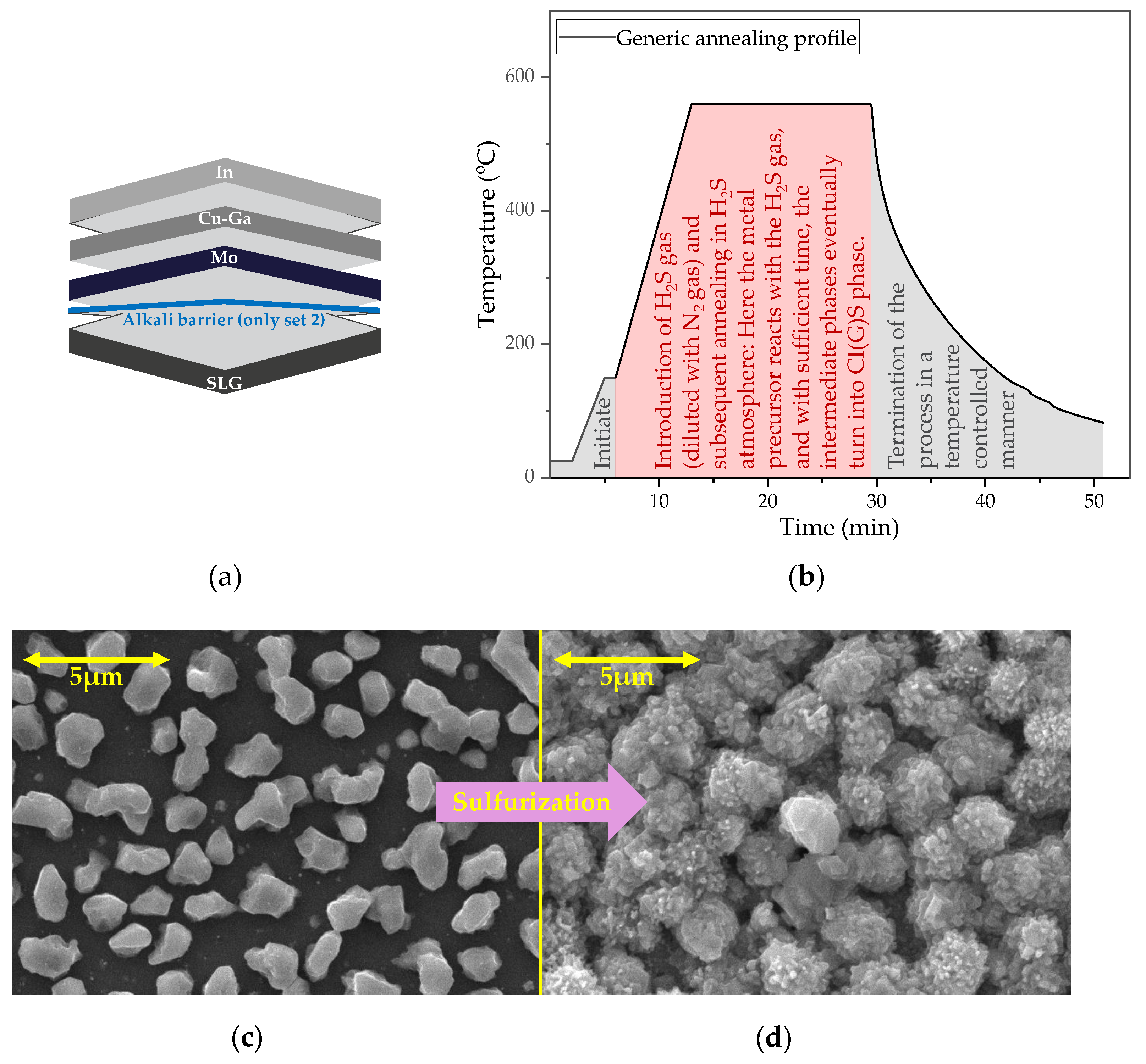
The raw materials used in the study (precursors) are presented first. Afterwards, the methodology and tools of the fabrication and characterization of the absorber layers and solar cells are discussed.

2.1. The Precursors

The schematics of the two sets of samples used in this study are illustrated in Figure 1a. For the first set, an indium layer was deposited onto a copper gallium matrix, which itself was deposited onto a molybdenum layer. This stack would prevent the formation of detrimental Cu-In alloys [18]. A 3-mm-thick soda-lime glass (SLG) functions as a substrate to the entire stack. The other set was prepared by including an alkali diffusion barrier (SiON) between the Mo and SLG substrates. This would help us determine the impact of presence of such a layer on the performance of the material and devices. CGI ([Cu]/([Ga] + [In])) and GGI ([Ga]/([Ga] + [In])) ratios of 0.9 and 0.25 were foreseen for both sets. A top-view SEM image from the indium hillocks on top of the Cu–Ga matrix is shown in Figure 1c.

2.2. The Absorber Layers

The precursors discussed above were cut into 2.5 ∗ 5 cm2 test pieces and processed in an Annealsys AS-ONE rapid thermal processing (RTP) system to develop absorber layers. Hereafter referred to as the baseline, a sulfurizing recipe, which results in an active absorber layer, was first designed. The rest of the experiments were based on this baseline with a generic profile as shown in Figure 1b.
As illustrated in Figure 1b, the recipe consists of a quick temperature stabilizing stage at 150 °C, followed by introducing hydrogen sulfide (H2S) and nitrogen (N2) gases at a temperature of 150 °C and a combined pressure of 200 mbar. The system is then ramped up to a sulfurization anneal at 560 °C. After 15 min of annealing, the system is cooled down in a controlled manner to 150 °C, before the termination of the process and a return to room temperature. The typical resultant μ-structure is depicted in Figure 1d.
In this scheme, the effect of changing five possibly influential factors was investigated on both sets of samples through the one-variable-at-a-time (OVAT) methodology. Each of the processing parameters was given a lower and higher value with respect to the baseline, and an experiment was run per combinations of factor levels, e.g., a run (interchangeably referred to as treatment in this work) with all factors at the baseline level, except at a longer annealing duration. These factors, their coded names and their corresponding levels for the experiments are summarized in Table 1. The baseline code is CP (Center Point).
The CP levels were chosen based on existing know-how in the group. The low and high levels were then chosen based on a variety of reasons, i.e., hardware limits and thermodynamics. Regarding the factors themselves, we tried to create a recipe as simple as possible; hence, only one annealing stage. It was then aimed to include all the essential processing parameters in the recipe.
Right after the sulfurization process, every produced absorber was characterized for photoluminescence peak position and minority carriers’ lifetime decay component (LT) using a Picoquant FluoTime 300 photoluminescence spectroscopy system with an excitation wavelength of 532 nm (25 ps, 3 MHz). Samples were then examined for roughness via a Keyence laser-equipped optical microscope, visually analyzed by a Bruker Tescan scanning electron microscopy (SEM) and chemically studied with an energy dispersive X-ray spectroscopy (EDX) module integrated into the SEM system.

2.3. The Solar Cell Devices

For each factor, the level treatment which produced a comparatively higher quality absorber were developed to complete solar cell devices: Fifty nanometers of cadmium sulfide (CdS) were deposited through a chemical bath deposition to form a buffer layer on the absorbers. Afterwards, 120 nm of i-ZnO and 250 nm of aluminum-doped ZnO were deposited as a window layer on top of CdS. Lastly, 50 nm of nickel and 1μm of aluminum were thermally evaporated onto the stack as contact grids. Figure 2a portrays a schematic of the layers stack. The cell area was then mechanically scribed to form 16 isolated devices manually, with an area of ~0.5 cm2 per cell. These are schemed in Figure 2b. Lastly, the back contact was formed by scratching the stack to the Mo level and soldering a small amount of indium on it.
The solar cells were then electrically measured at room temperature under a current-voltage (I-V) system using a 2401 Keithley source meter under a simulated A.M 1.5-G spectrum with an illumination density of 1000 Wm−2. Data were extracted by fitting a single diode model. An integrated heating plate was used occasionally for measurements at different temperatures of interest. Moreover, an external quantum efficiency (EQE) analysis was carried out on the samples of interest using an in-house setup.
Furthermore, to analyze the present crystalline phases, the XRD measurements were done at the device level, with an X'pert XRD diffractometer from PANanalytical with a Cu Kα1 radiation source and in θ-2θ Bragg-Brentano geometry.

3. Results and Discussion

Here, we discuss the effects of different processing parameters for the case of absorber layers and solar cell devices separately. For the former, the results are discussed in terms of the minority carriers' lifetimes and surface roughness. As for the latter, the usual device parameters extracted from the I–V measurements (efficiency (Eff), fill factor (FF), open-circuit voltage (VOC) and short circuit current (JSC)) were analyzed. This would help us in investigating an objective correlation between the performances of absorbers and resulting devices.

3.1. The Absorber Layers

The EDX results of the absorber layers indicated an average CGI ratio of 0.89 and coefficient of variation (CV = standard deviation/average) of 4%. This would indicate the relative robustness of the composition under different processing conditions and that nearly all the absorbers belong to the copper-poor region. This compactness is also reflected in the records of the photoluminescence peak position, where all the absorbers averaged a bandgap value of 1.47 eV with a CV of 2%. To this end, the PL peak position was not further considered in filtering out unimportant factors.
Regarding both the lifetime and roughness, the omission of a barrier layer has generally caused a more diverse set of data. In other words, samples without a barrier layer appeared more sensitive to changes in the processing parameters. This is visually illustrated in the dot plots illustrated in Figure 3a and backed by the numbers in Table 2.
As evident, the absorbers generally showed a higher lifetime (and less roughness) in the absence of a barrier layer. For instance, as illustrated in Figure 3b, in 63 percent of the pairs (= samples with and without a barrier under the same processing conditions), those without a diffusion barrier layer (-Bar) featured a slightly higher average LT value. This could be attributed to possible alkali provision by the substrate (SLG) [20] and via the deactivation of copper vacancies with sodium [21].
On the other hand, while the process smoothened the precursor’s surface by ~100 nm, the films’ generally rough surface was not unexpected, given the typical surfaces known in CIGS absorbers developed via a two-step sequential route [22].
Additionally, there appeared to be a mild correlation between the roughness and LT data. In 63% of the pairs (rising to 81% when including D and CP), when a barrier existed, the lifetime was less, and the roughness was higher. This could be attributed to the detrimental effect of roughness to the LT by providing recombination centers at the surface.
As such, these results indicate a general improvement of the absorbers when the path for alkali diffusion from the substrate is open.
Lastly, Table 3 summarizes the relative distance of each treatment's LT to the baseline, using the percent error as the statistic. The same is also reported for roughness. Such data helps in identifying the processing parameters that impacted the quality of the absorbers the most, with higher values indicating higher impacts. Note that 30 percent, the yellow numbers (underlined), is the error value where the boundary was set to distinguish between significant and nonsignificant error terms, and red numbers (double underlined) indicate cases where highest errors occurred. As can be seen in both types of absorbers (+Bar and -Bar), factors A, C and E caused the most differences. Among these, the annealing temperature (factor A) was already a point of interest given the previous literature [17] and was a suspect from the beginning, given that primary chalcopyrite phase formation takes place in this step. However, the absence of an annealing duration was unforeseen; it could be that the minimum extreme duration is already enough, and the maximum extreme does not change the phase and crystals to a great extent.
Furthermore, with the aid of the CP treatment, it was investigated whether the factors affect the absorbers independent of each other or if there exist interactions between them. This was done through linearly regressing each response (LT and roughness), with the factor levels as the regressors, and evaluating the R a d j 2 statistic. This statistic adjusts the R 2 (square of r in (1)) and describes how close the regressed data is to the linear fit. Therefore, the higher the statistic value, the closer the data to the fitted line and, in turn, the higher degree of independency for a factor’s impact on the absorber. This analysis was done for all the factors and reported for the samples with and without a barrier layer in Table 4.
High values of R a d j 2 are colored in red and double-underlined for ease of finding them. As can be seen, factors A, B and C indicate nonlinearity in both of their response variables (LT and roughness). This suggests that these processing parameters do not influence the absorbers independently. Thus, it can be assumed that a degree of interaction exists between the factors recognized in this study or with some other processing parameters unrecognized here. On the other hand, factor E appeared to affect the roughness of the absorbers independent from the other factors and regardless of the use of a barrier. To a lesser extent, lifetime of barrierless samples could also be independently influenced by changes in factors B and D. However, as no pair of metrics for these two parameters pointed in the same direction, it could still mean the presence of interactions between the processing parameters.

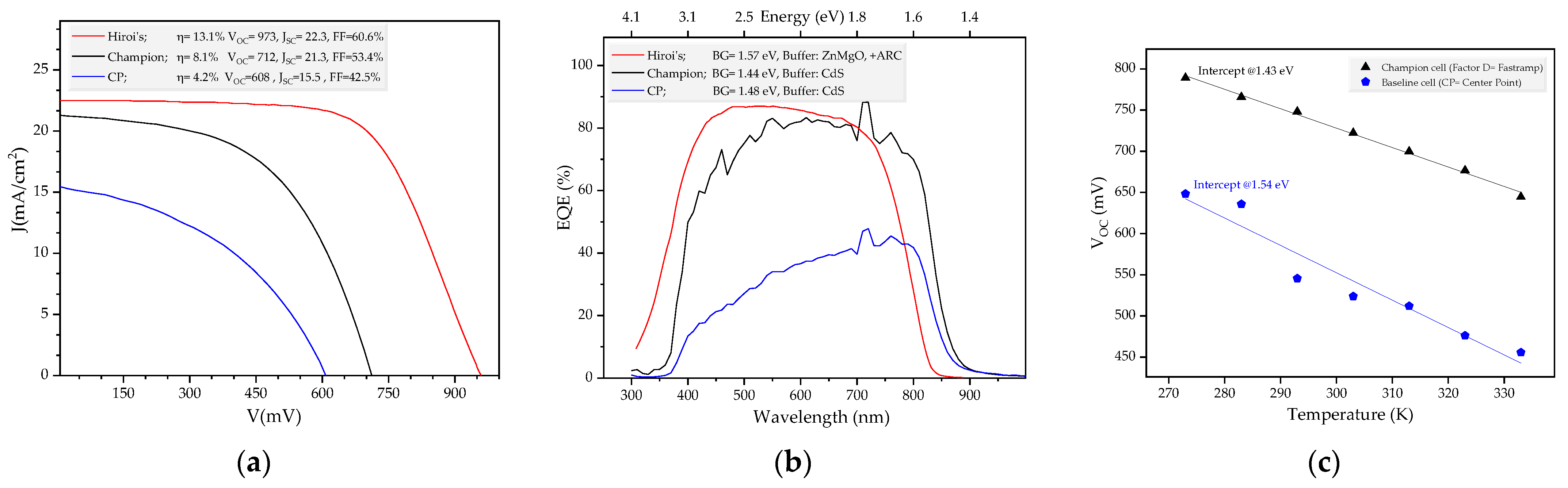
3.2. The solar Cell Devices

The device parameters are detailed in the trellis plots of Figure 4. Note that each point represents an average value of four different measurements per sample for each metric. Same as before, whether a sample had a diffusion barrier or not is indicated in the panel headers with ±Bar. Additionally, note that, in Figure 4b, the absorbers' LT average values are reported on the same axis as the efficiency for each treatment.
The samples without a barrier layer generally appeared to show higher JSC and VOC responses than the samples with a barrier layer. This could be attributed to the possible inclusion of light alkalis from the substrate [20] and their positive effects on the passivation of bulk defects [23], an increase of the doping levels [24,25] or the facilitated growth of the CIGS phase [26]. This is especially notable in the treatment of factor D, which produced the best cells between all treatments.
Figure 5a illustrates the electrical behavior of this work's baseline (CP) and champion cell (Factor D, where a faster ramp rate was employed). Note that both instances belonged to the samples without a barrier layer. For comparison, the data were extracted using a graph digitizer from a publication by Hiroi et al. on their world record pure sulfide CIGS solar cell [27], where they also achieved improved cells by employing a fast ramp and promoting a steeper gallium profile at the back. While our champion cell was significantly improved in both the short-circuit current and open-circuit voltage by tuning the ramp rate, it still suffered a considerably lower VOC than Hiroi’s.
Analyzing the EQE plot in Figure 5b, losses at high energies of above 2.4 eV could be associated with quality and thickness of CdS buffer layer (with a bandgap of ~2.43 eV), and with the emitted electron–hole pairs not getting collected. A concern actually addressed in the work of others and Hiroi’s, (partially) by using alternative/thicker buffer/window layers and increasing the relative work function [11,13,27,28].
At the lower energies of below 1.8 eV, the losses originate primarily from incomplete or less absorption and generation in the absorber layer. This is understandable given the lower bandgap of our cells compared to Hiroi’s, which can result from less Ga incorporation. The XRD analysis (not shown) approved that the developed crystals were mainly of the CuInS2 phase, which has a bandgap of ~1.5 eV [4]. Our sample’s bandgap was also investigated through calculating the VOC in temperature-dependent I–V measurements (see Figure 5c). The extracted values for the bandgaps (intercepts of the linear fit in Figure 5c) equal almost exactly our PL data from champion cell (Factor D = Fastramp) and is only marginally different in the case of the baseline.
This lack of gallium at the front side could be a side effect of the two-step processing method, as previous works also suggested that this technique could hinder Ga incorporation in the active region of the CIGS layer [29,30]. Lastly, shading, reflection and that we did not apply an antireflection coating also played a role in less EQE values than Solar Frontier’s work [31].

3.3. Curvature in Response

To investigate an objective correlation between the absorber and device metrics, we used the Pearson product moment correlation coefficient statistic (r in (1)), which indicates the strength of a linear correlation between a pair of data [32]:
r =   [ ( x i x ¯ ) ( y i y ¯ ) ]   ( x i x ¯ ) 2 ( y i y ¯ ) 2 ,
where x i and y i denote the induvial metric values in the ith treatment for the two correlated metrics, and x ¯ and y ¯ denote the metric’s means.
The scatter matrix in Figure 6 aids readers to visually inspect the spread of the data. Note that the values for the best device—that is, for Factor ±D are not included, as this device performed significantly better compared to the others.
The absorbers' roughness showed a significant negative linear correlation with the efficiency (and fill factor) (see the r values reported at the bottom of each cell in Figure 6). In fact, when the same procedure was applied only on the samples without a barrier (-Bar), roughness complied more with the essential assumptions of the statistic and was even more strongly linearly correlated with the efficiency (r = −0.87). Still, as the bivariate normality requirement for the utilization of Pearson’s statistics was violated in most cases [33], credible conclusions could not be drawn. Nevertheless, it seems that, except for roughness in the samples without an alkali barrier, no linear association between the data exists, even by visual inspection.

4. Conclusions and Outlook

The absence of an alkali diffusion barrier had the most significant effect on our absorbers’ quality. Three processing parameters proved dominant in dictating the lifetime and roughness of the absorbers: annealing temperature, sulfur agent (H2S) introduction temperature and subsequent pressure. Furthermore, our data suggested the existence of interactions between the processing parameters. The specifics of such interactions could be the subject of future studies.
Looking at the data of the solar cells, the ramp rate to the sulfurization anneals played a key role in attaining high-performing devices. Moreover, a strong negative linear correlation between roughness and device efficiency was observed for samples without an alkali diffusion barrier.
Meanwhile, a path to develop above 8 percent pure sulfide CIGS solar cells was established using a two-step sequential processing method and room for improvement were identified. Roughness of the absorber layers exhibited a strong negative impact on the performances of devices. The type, quality and thickness of the employed buffer layer proved to be of high importance in attaining an efficient solar cell based on our EQE results. Therefore, these are suggested to be the critical areas to study in the future and improve this state-of-the-art technology.

Author Contributions

Conceptualization, G.B.; methodology, G.B. and S.H.; validation, S.H.; formal analysis, G.B. and S.H.; investigation, S.H.; resources, M.M.; data curation, B.V.; writing—original draft preparation, S.H.; writing—review and editing, S.H., G.B., M.M., J.P. and B.V.; visualization, S.H.; supervision, G.B. and B.V.; project administration, B.V. and funding acquisition, B.V. All authors have read and agreed to the published version of the manuscript.

Funding

This project received funding from the European Union's Horizon 2020 Research and Innovation Program under grant agreement No. 640868.

Institutional Review Board Statement

Not applicable.

Informed Consent Statement

Not applicable.

Data Availability Statement

The data presented in this study are available upon request from the corresponding author.

Conflicts of Interest

The authors declare no conflict of interest. The funders had no role in the design of the study; in the collection, analyses or interpretation of the data; in the writing of the manuscript or in the decision to publish the results.

References

  1. Kageshima, Y.; Shiga, S.; Kumagai, H.; Teshima, K.; Domen, K.; Nishikiori, H. Photoelectrochemical Properties of Particulate CuGaSe2 and CuIn0. 7Ga0. 3Se2 Photocathodes in Nonaqueous Electrolyte. Bull. Chem. Soc. Jpn. 2020, 93, 942–948. [Google Scholar] [CrossRef]
  2. Yuan, J.; Hao, C. Solar-Driven Photoelectrochemical Reduction of Carbon Dioxide to Methanol at CuInS2 Thin Film Photocathode. Sol. Energy Mater. Sol. Cells 2013, 108, 170–174. [Google Scholar] [CrossRef]
  3. Feurer, T.; Reinhard, P.; Avancini, E.; Bissig, B.; Löckinger, J.; Fuchs, P.; Carron, R.; Weiss, T.P.; Perrenoud, J.; Stutterheim, S. Progress in Thin Film CIGS Photovoltaics–Research and Development, Manufacturing, and Applications. Prog. Photovolt. Res. Appl. 2017, 25, 645–667. [Google Scholar] [CrossRef]
  4. Tell, B.; Shay, J.L.; Kasper, H.M. Electrical Properties, Optical Properties, and Band Structure of CuGaS2 and CuInS2. Phys. Rev. B 1971, 4, 2463–2471. [Google Scholar] [CrossRef]
  5. Tinoco, T.; Rincón, C.; Quintero, M.; Pérez, G.S. Phase Diagram and Optical Energy Gaps for CuInyGa1−ySe2 Alloys. Phys. Status Solidi A 1991, 124, 427–434. [Google Scholar] [CrossRef]
  6. Guillemoles, J.; Rau, U.; Kronik, L.; Schock, H.; Cahen, D. Cu(In,Ga)Se2 Solar Cells: Device Stability Based on Chemical Flexibility. Adv. Mater. 1999, 11, 957–961. [Google Scholar] [CrossRef]
  7. de Wild-Scholten, M.J. Energy Payback Time and Carbon Footprint of Commercial Photovoltaic Systems. Sol. Energy Mater. Sol. Cells 2013, 119, 296–305. [Google Scholar] [CrossRef]
  8. Jordan, D.C.; Kurtz, S.R.; VanSant, K.; Newmiller, J. Compendium of Photovoltaic Degradation Rates. Prog. Photovolt. Res. Appl. 2016, 24, 978–989. [Google Scholar] [CrossRef]
  9. Brenner, W.; Adamovic, N. Thin-Film CIGS Solar Modules for Design Driven Applications in the Frame of the FP7 NMP Project SolarDesign. In Proceedings of the 2015 38th International Convention on Information and Communication Technology, Electronics and Microelectronics (MIPRO), Oatija, Croatia, 25–29 May 2015; pp. 131–136. [Google Scholar]
  10. Kazmerski, L.L.; Sanborn, G.A. CuInS2 Thin-film Homojunction Solar Cells. J. Appl. Phys. 1977, 48, 3178–3180. [Google Scholar] [CrossRef]
  11. Hiroi, H.; Iwata, Y.; Adachi, S.; Sugimoto, H.; Yamada, A. New World-Record Efficiency for Pure-Sulfide Cu(In,Ga)S2 Thin-Film Solar Cell With Cd-Free Buffer Layer via KCN-Free Process. IEEE J. Photovolt. 2016, 6, 760–763. [Google Scholar] [CrossRef]
  12. Nishimura, T.; Kim, S.; Chantana, J.; Kawano, Y.; Ishizuka, S.; Minemoto, T. Application of Al-Doped (Zn, Mg)O on Pure-Sulfide Cu(In, Ga)S2 Solar Cells for Enhancement of Open-Circuit Voltage. Sol. Energy Mater. Sol. Cells 2019, 202, 110157. [Google Scholar] [CrossRef]
  13. Shukla, S.; Sood, M.; Adeleye, D.; Peedle, S.; Kusch, G.; Dahliah, D.; Melchiorre, M.; Rignanese, G.-M.; Hautier, G.; Oliver, R.; et al. Over 15% Efficient Wide-Band-Gap Cu(In,Ga)S2 Solar Cell: Suppressing Bulk and Interface Recombination through Composition Engineering. Joule 2021, 1816–1831. [Google Scholar] [CrossRef]
  14. Kim, S.; Nagai, T.; Tampo, H.; Ishizuka, S.; Shibata, H. Large Open-Circuit Voltage Boosting of Pure Sulfide Chalcopyrite Cu(In,Ga)S2 Prepared Using Cu-Deficient Metal Precursors. Prog. Photovolt. Res. Appl. 2020, 28, 816–822. [Google Scholar] [CrossRef]
  15. He, G.; Yan, C.; Li, J.; Yuan, X.; Sun, K.; Huang, J.; Sun, H.; He, M.; Zhang, Y.; Stride, J.A.; et al. 11.6% Efficient Pure Sulfide Cu(In,Ga)S2 Solar Cell through a Cu-Deficient and KCN-Free Process. ACS Appl. Energy Mater. 2020, 3, 11974–11980. [Google Scholar] [CrossRef]
  16. Merdes, S.; Abou-Ras, D.; Mainz, R.; Klenk, R.; Lux-Steiner, M.C.; Meeder, A.; Schock, H.W.; Klaer, J. CdS/Cu(In,Ga)S2 Based Solar Cells with Efficiencies Reaching 12.9% Prepared by a Rapid Thermal Process. Prog. Photovolt. Res. Appl. 2013, 21, 88–93. [Google Scholar] [CrossRef] [Green Version]
  17. Lomuscio, A.; Rödel, T.; Schwarz, T.; Gault, B.; Melchiorre, M.; Raabe, D.; Siebentritt, S. Quasi-Fermi-Level Splitting of Cu-Poor and Cu-Rich CuInS2 Absorber Layers. Phys. Rev. Appl. 2019, 11, 054052. [Google Scholar] [CrossRef] [Green Version]
  18. Kwon, I.; Nagai, T.; Ishizuka, S.; Tampo, H.; Shibata, H.; Kim, S.; Kim, Y. Improving the Performance of Pure Sulfide Cu(InGa)S2 Solar Cells via Injection Annealing System. Curr. Appl. Phys. 2021, 22, 71–76. [Google Scholar] [CrossRef]
  19. Kato, T. Cu(In,Ga)(Se,S)2 Solar Cell Research in Solar Frontier: Progress and Current Status. Jpn. J. Appl. Phys. 2017, 56, 04CA02. [Google Scholar] [CrossRef]
  20. Salomé, P.M.P.; Rodriguez-Alvarez, H.; Sadewasser, S. Incorporation of Alkali Metals in Chalcogenide Solar Cells. Sol. Energy Mater. Sol. Cells 2015, 143, 9–20. [Google Scholar] [CrossRef]
  21. Oikkonen, L.; Ganchenkova, M.; Seitsonen, A.; Nieminen, R.M. Effect of Sodium Incorporation into CuInSe2 from First Principles. J. Appl. Phys. 2013, 114, 083503. [Google Scholar] [CrossRef] [Green Version]
  22. Kamikawa, Y.; Nishinaga, J.; Shibata, H.; Ishizuka, S. Efficient Narrow Band Gap Cu(In,Ga)Se2 Solar Cells with Flat Surface. ACS Appl. Mater. Interfaces 2020, 12, 8. [Google Scholar] [CrossRef]
  23. Abou-Ras, D.; Wagner, S.; Stanbery, B.J.; Schock, H.-W.; Scheer, R.; Stolt, L.; Siebentritt, S.; Lincot, D.; Eberspacher, C.; Kushiya, K.; et al. Innovation Highway: Breakthrough Milestones and Key Developments in Chalcopyrite Photovoltaics from a Retrospective Viewpoint. Thin Solid Film 2017, 633, 2–12. [Google Scholar] [CrossRef]
  24. Deprédurand, V.; Tanaka, D.; Aida, Y.; Carlberg, M.; Fèvre, N.; Siebentritt, S. Current Loss Due to Recombination in Cu-Rich CuInSe2 Solar Cells. J. Appl. Phys. 2014, 115, 044503. [Google Scholar] [CrossRef]
  25. Nakada, T.; Iga, D.; Ohbo, H.; Kunioka, A. Effects of Sodium on Cu(In,Ga)Se2-Based Thin Films and Solar Cells. Jpn. J. Appl. Phys. 1997, 36, 732–737. [Google Scholar] [CrossRef]
  26. Hergert, F.; Hock, R.; Weber, A.; Purwins, M.; Palm, J.; Probst, V. In Situ Investigation of the Formation of Cu(In,Ga)Se2 from Selenised Metallic Precursors by X-Ray Diffraction—The Impact of Gallium, Sodium and Selenium Excess. J. Phys. Chem. Solids 2005, 66, 1903–1907. [Google Scholar] [CrossRef]
  27. Hiroi, H.; Iwata, Y.; Sugimoto, H.; Yamada, A. Progress Toward 1000-MV Open-Circuit Voltage on Chalcopyrite Solar Cells. IEEE J. Photovolt. 2016, 6, 1630–1634. [Google Scholar] [CrossRef] [Green Version]
  28. Jäger, T.; Romanyuk, Y.E.; Bissig, B.; Pianezzi, F.; Nishiwaki, S.; Reinhard, P.; Steinhauser, J.; Schwenk, J.; Tiwari, A.N. Improved Open-Circuit Voltage in Cu(In,Ga)Se2 Solar Cells with High Work Function Transparent Electrodes. J. Appl. Phys. 2015, 117, 225303. [Google Scholar] [CrossRef] [Green Version]
  29. Klenk, R.; Bakehe, S.; Kaigawa, R.; Neisser, A.; Reiß, J.; Lux-Steiner, M.C. Optimising the Open-Circuit Voltage of Cu(In,Ga)S2 Solar Cells—Design and Analysis. Thin Solid Film 2004, 451–452, 424–429. [Google Scholar] [CrossRef]
  30. Neisser, A.; Hengel, I.; Klenk, R.; Matthes, T.W.; Álvarez-García, J.; Pérez-Rodíguez, A.; Romano-Rodíguez, A.; Lux-Steiner, M.-C. Effect of Ga Incorporation in Sequentially Prepared CuInS2 Thin Film Absorbers. Sol. Energy Mater. Sol. Cells 2001, 67, 97–104. [Google Scholar] [CrossRef]
  31. Hegedus, S.S.; Shafarman, W.N. Thin-Film Solar Cells: Device Measurements and Analysis. Prog. Photovolt. Res. Appl. 2004, 12, 155–176. [Google Scholar] [CrossRef]
  32. Dodge, Y. The Concise Encyclopedia of Statistics; Springer Science & Business Media: Berlin/Heidelberg, Germany, 2008; ISBN 0387317422. [Google Scholar]
  33. Schober, P.; Boer, C.; Schwarte, L.A. Correlation Coefficients: Appropriate Use and Interpretation. Anesth. Analg. 2018, 126, 1763–1768. [Google Scholar] [CrossRef] [PubMed]
Figure 1. Precursor stack (a), its top view (c), generic annealing profile (b) and CIGS layer top view (d).
Energies 14 04737 g001
Figure 2. Schematic of the solar cell devices stack (a) and top view (b).
Energies 14 04737 g002
Figure 3. Lifetime and roughness behaviors of samples with and without a barrier (a) and samples per factor-level barrier (b).
Energies 14 04737 g003
Figure 4. Solar cell device parameters JSC and VOC (a) and the Eff, FF and absorber LT (b).
Energies 14 04737 g004
Figure 5. J-V (a), EQE (b) and temperature-dependent VOC (c) of this work’s baseline and best cells.
Energies 14 04737 g005
Figure 6. Scatter matrix plot for the pairs of metrics annotated with Pearson’s coefficient (r).
Energies 14 04737 g006
Table 1. Processing parameters and respective levels.
CodesProcessing ParameterLevel
Low (-)Baseline (CP)High (+)
AAnneal temp 1 (°C)520560600
BAnneal dur 2 (min)51545
CH2S press 3 (mbar)5200200 *
DRamp rate (°C/s)0.215
EH2S intro temp (°C)50150350
1 Temperature. 2 Duration. 3 Pressure. * Only H2S.
Table 2. Spread of data for the absorbers. The average value is followed by the coefficient of variation (CV).
MetricSample
+Bar-BarAll
Lifetime2.13 ns (CV = 20%)2.54 ns (CV = 36%)2.33 ns (CV = 30%)
Roughness310 nm (CV = 10%)280 nm (CV = 17%)292 nm (CV = 14%)
Table 3. Relative distance to the CP, reported in percent error, for the LT and roughness of all the absorbers.
Barrier+Bar-Bar
MetricLifetimeRoughnessLifetimeRoughness
Level-+-+-+-+
Factor codes
- See Table 1 for reference
A301918413875
B15743143132
C113340.1194014040
D112741116301
E30144224561836
Red numbers are farthest from the CP, and yellows are marginally different.
Table 4. R a d j 2 (%) for the response variables per each factor. See Table 1 for the references to the factor codes.
Barrier+Bar-Bar
MetricLifetimeRoughnessLifetimeRoughness
Factor codesA−7129~054
B26−1566−37
C22201576
D−992969−86
E−7943586
Publisher’s Note: MDPI stays neutral with regard to jurisdictional claims in published maps and institutional affiliations.

