Article

Effect of Various Wafer Surface Etching Processes on c-Si Solar Cell Characteristics

1
Department of Electronic Engineering, Korea National University of Transportation, Chungju 27909, Korea
2
Jeonnam Technopark, #370, Green-ro, Jeollanam-do 58324, Korea
3
Department of IT Energy Convergence, Korea National University of Transportation, Chungju 27909, Korea
*
Author to whom correspondence should be addressed.
Energies 2021, 14(14), 4106; https://doi.org/10.3390/en14144106
Submission received: 9 June 2021 / Revised: 1 July 2021 / Accepted: 5 July 2021 / Published: 7 July 2021
(This article belongs to the Section D1: Advanced Energy Materials)

Abstract

:
In order to analyze the effects of various sizes of pyramid structure on solar cell characteristics, a pyramid structure was formed on the wafer through various etching processes. In this paper, etching was performed using one-step etching processes such as alkaline solution etching, reactive ion etching (RIE), and metal-assisted chemical etching (MACE), and two-step etching processes such as alkaline solution + MACE and alkaline solution + RIE. The micro-sized pyramid-structured wafers formed using the alkali solution showed higher reflectivity than nano-sized pyramid-structured wafers. Accordingly, it was expected that the characteristics of the cells fabricated with a nano-sized pyramid-structured wafer having low reflectivity would be higher than that of a micro-sized pyramid-structured wafer. However, it was confirmed that the quantum efficiency characteristics in the short wavelength region were higher in the micro-sized pyramid-structured wafers than in the nano-sized pyramid-structured wafers. To confirm the reason for this, surface characteristics were analyzed through the deposition of an emitter layer on a wafer formed in a pyramidal structure. As a result, in the case of the nano-sized pyramid-structured wafer, the sheet resistance characteristics were lower due to the increased depth of the emitter layer in comparison to the micro-sized pyramid-structured wafer. Accordingly, it was determined that the quantum efficiency was degraded as a result of the high recombination rate.

1. Introduction

Photovoltaic (PV) power generation is a very popular energy resource due to its eco-friendly and infinite nature. The current PV market has exceeded 627 GW of accumulated installed capacity in 2019, and this is expected to increase further over time. As PV power generation presents the possibility of making leaps in technology when compared to national investment, it is time to secure various researches and technologies to extract maximum performance as a continuous energy supply source [1]. Currently, the main areas of interest in the photovoltaic field can be divided into two. The first area regards the development of high-efficiency solar cells to improve solar power generation efficiency. Various high-efficiency solar cell structures based on c-Si have been proposed. Examples of high-efficiency solar cell technology include: passivated emitter and rear cell (PERC) structured solar cells [2], manufactured by the insertion of anti-reflection film onto the back of a solar cell; LDSE structure solar cells [3] with a selective emitter applied; a bifacial solar cell with two-sided absorbing solar cells [4]; and tandem solar cells using perovskite solar cells [5,6] as upper cells. The second area of interest revolves around lowering the costs of manufacturing PV cells. The materials that cost the most during the manufacture of solar cells are the wafer and silver paste. In order to manufacture a low-cost solar cell, it is essential to thin the wafer and reduce the amount of silver paste used. Si wafers have the highest share in price determination and research for the commercialization of c-Si solar cells containing a thinner structure is actively underway. As the thickness of the wafer decreases in order to reduce costs, the process method of wafers 180 to 200 μm thick, which are commercially available, must be improved. For example, a wafer surface etching process using wet etching that consumes a large amount of Si is difficult to apply to a thin wafer. In order to compensate for this, various surface etching processes using reactive ion etching and metal catalytic chemical etching have been developed. In order to obtain a low-cost and high-efficiency solar cell, it is necessary to improve the process method while taking into account factors that reduce the efficiency of the solar cell. Factors that reduce the efficiency of a solar cell can be largely divided into recombination loss, resistance loss, and optical loss. Recombination loss is the process by which electrons and holes separated by light are recombined before being collected in the metal electrode, accordingly, it does not contribute to solar cell efficiency. In order to reduce recombination loss on the upper surface of a solar cell, a method is generally applied to reduce the number of dangling bonds on the surface by forming a passivation layer. In the case of rear surface recombination, this can be compensated for through the formation of a rear electric field with high concentration doping [7]. Loss due to resistance components can be divided into series resistance and parallel resistance, and various studies are being conducted to reduce each loss. The first factor that causes optical loss is shadow loss due to the front electrode. In a typical solar cell, an electrode is formed on the front surface of the light incident, and shadow loss occurs because the electrode cannot absorb light in the formed portion. In addition, optical loss is mainly caused by reflections occurring on the Si surface depending on the wavelength of the sunlight. In general, the surface of a Si wafer reflects more than 30% of light on average at a wavelength of 400~1000 nm [8,9]. Solar cells can absorb light and create pairs of electrons and holes. However, when light is reflected from the surface of the solar cell, it eventually cannot be absorbed and thus does not generate electron and hole pairs. This decreases the short-circuit current of the solar cell and causes the output of the module to decrease [10]. In this paper we studied the effects on solar cell characteristics when minimizing optical loss across various efficiency loss factors. The etching process of the c-Si wafer increases the amount of absorbed light by increasing the passage length of light in the solar cell through a reduction of surface reflectance of incident light. Accordingly, the reduction of short-circuit current due to light reflection can be improved. The etching rate varies depending on the direction of the Si crystal, and a pyramid is formed on the wafer surface using the difference in the etching rate. The etching rate is fastest in the (100) direction surface of the wafer, and the etching rate in the (111) direction decreases about 1/100 times, thereby obtaining a pyramid shape [11]. In the wafer on which the pyramid structure is formed, light is incident again to the substrate by the inclined surface, thus enabling increased absorption. The pyramid structure formed on the surface of c-Si plays an important role in the direction of light according to the formation angle. Figure 1 shows the path of light incident on the V-shaped surface according to the angle. At α = 30 ° , only the lower part of the V-shaped groove has a path through which light is reflected twice, and at α = 45 ° all incident light has a path through which it is reflected twice. At α = 54 ° , only the lower part of the V-shaped groove has a path through which light is reflected three times, and at α = 60 ° all incident light has a path through which it is reflected three times. As the angle of the pyramid structure increases, the number of reflections increases, and the amount of light generated electrons increases.
Accordingly, increasing the absorption of light through the number of reflections can be directly related to the efficiency of the solar cell, so that the degree of curvature formed on the surface can contribute to the improvement of the efficiency of the solar cell. A solar cell having a micro-sized pyramid structure can control the average reflectance to less than 10%, and a solar cell having a nano-sized pyramid structure can improve short-circuit current by reducing reflectance [12]. There are methods of forming various wafer surfaces, such as a micro-sized pyramid structures and nano-sized pyramid structures. Methods for forming micro-sized pyramid structures include alkali solution etching, reactive ion etching (RIE), and metal-assisted chemical etching (MACE). The pyramid formation method using an alkali such as NaOH and KOH solutions is the most widely used, and anisotropic etching is performed according to the crystal orientation of the c-Si solar cell. Dissolving a specific surface faster than other surfaces is called anisotropic etching or anisotropic etching. Anisotropic etching is mainly used for the surface treatment of single c-Si wafers, and an alkali solution of sodium hydroxide (NaOH) and potassium hydroxide (KOH) is used. The mechanism of anisotropic etching is as follows. The Si surface is oxidized by OH ions, and sodium silicate (K2SiO3) is formed through combination with K+ and Na+ ions [13]. RIE is a method of etching by simultaneously performing physical collisions and chemical reactions caused by plasma [14]. During the etching reaction by plasma, radicals and ions are adsorbed on the surface of the Si wafer, and a reactant is formed through a chemical reaction. The formed reactants are desorbed, and the desorbed reactants are discharged out of the chamber. The gases used for etching are Si etching gases, such as Cl2 and SF6, which are difficult to manage due to toxicity and explosion characteristics. For this reason, processes using SF6 and O2 gases, which are relatively easy to manage and non-toxic fluorine gases, are widely used. At this time, SF6 is composed of neutrons, electrons, photons, radicals (F*), cations (SF5+), and anions (F). O2 is composed of radicals (O*), and glow discharge is generated by the dissociation and ionization of electron collisions. The MACE is an etching method using a metal catalyst such as Ag or Cu. An oxidation reaction occurs at the interface between the silicon surface and the deposited metal catalyst, and a cathode reaction occurs where the metal and the solution exist [15,16,17]. In this paper, pyramid shapes of various sizes were implemented onto the wafer by using various etching processes such as etching using an alkaline solution, reactive ion etching, and metal-assisted chemical etching. Accordingly, when the optical loss through the reduction of the wafer’s reflectance was minimized by using various etching processes, we studied how all cell characteristics were affected. The paper is written in two parts. The first section regards the surface etching process optimization according to various methods, and the second section outlines the effects of the doping layer according to the surface structure of the wafer. In the first topic, the influence of the doping layer according to various surface textures was comparatively analyzed. As was expected, the cell characteristics had a greater effect on the doping layer than on the electrode and surface passivation. The doping layer was formed through use of a furnace according to the surface structure of the wafer, and a comparative analysis was conducted. The second topic regards the analysis method of the doping layer. It is very important to measure the profile of the doping concentration distribution and doping depth after the emitter formation process. In general, doping profile is mainly measured using SIMS (secondary ion mass spectroscopy), ECV (electrochemical capacitance-voltage), or KFM (Kelvin probe force microscope) analysis methods. In this paper, instead of the SIMS, ECV, and KFM analysis methods, a selective etching method (SE) for analysis using a scanning electron microscope (SEM) was performed to analyze the doped layer after forming a step by using the difference in etching rate between the emitter layer and the non-emitter layer. Accordingly, compared to existing analysis methods, the doped layer can be analyzed using an easier and cheaper solution such as HF, H2O2, or H2O.

2. Materials and Methods

In order to analyze the cell characteristics according to the pyramidal structure by performing various surface etching, a p-type single c-Si wafer of 15.675 × 15.675 cm2 was used. First, to remove impurities from the wafer substrate before performing the surface etching, ultrasonic cleaning was performed for 10 min in the order of acetone, methanol, and DI water. After removing metal impurities with a 10% HCl solution and removing the natural oxide film with a 10% HF solution, the wafer was sufficiently washed with DI water and then dried with nitrogen. After performing the wafer cleaning process, the etching process was carried out through five etching methods. The surface etching processes included a surface etching process using an alkali solution of KOH, an etching process using RIE, an etching process using a Ag metal catalyst, and an etching process using two-step processes involving an alkali solution, RIE, and MACE. First, before proceeding with the wafer etching process, this process was performed after removing the surface cutting defects on the wafer surface using a KOH solution. Etching with an alkali solution, mainly KOH, was used for the surface treatment of the single c-Si wafers. In order to proceed, the etching process with alkali solution, KOH, IPA, and DI water was used. The etching process conditions were changed at 2 to 3 wt.% of KOH, 7.5 to 9 vol.% of IPA, and a process temperature of 80 °C to form a micro-sized pyramid on the surface [18]. The etching process using RIE was performed by forming a plasma using SF6 and O2 gases, which are fluorine gases, and using a chemical reaction with a Si wafer [19]. In the RIE process, the surface shape and reflectance characteristics of the wafer were analyzed by varying the gas ratio of SF6 and O2 from 5:1 to 1:2 and the etching time from 200 to 700 s. In the MACE process, a Ag metal catalyst is deposited on the Si surface and then immersed in a solution mixed with HF and H2O2 to etch using oxidation and reduction reactions occurring between the Si substrate and the metal particles [15]. As the metal catalyst, Ag metal particles having a thickness of 7 nm were deposited on the surface of a Si wafer using a thermal evaporator. After the deposition step, in order to observe any changes according to the etching time, the Si wafer deposited the Ag metal particles and was etched under the conditions of 30 to 360 s. Thereafter, after fixing the etching time, the characteristics of the wafer were analyzed by varying the ratio of the etching solutions. The etching process using KOH and RIE is an additional application of the RIE process utilized to form a nano-sized pyramid structure on wafer surfaces etched with KOH. In the etching process using KOH and MACE, a nano-structured pyramid is formed on a wafer surface-etched with KOH using a Ag metal catalyst. After forming a pyramid structure on the wafer surface using the five methods, the average reflectance of the wavelength of 400~1000 nm was measured with a UV/VIR spectrometer, and the pyramid structure was confirmed through field emission scanning electron microscope (FE-SEM) images [20]. In order to analyze the characteristics according to the pyramid structure when fabricating the wafer surface-etched through five methods into cells, an emitter formation process was performed using a furnace. In order to analyze the effects of the pyramid structure formed on the wafer on the emitter formation process, POCl3 gas was introduced into the furnace using a POCl3 liquid source as raw material. After pre-deposition at a temperature of 825 °C on the surface of the substrate, this was diffused through high temperature heat of 845 °C [21,22]. Subsequently, the structural analysis in which the emitter layer was formed according to the pyramid structure was performed through SEM images, and quantum efficiency characteristics were compared to proceed with the electrical analysis based on the structural analysis of the emitter layer according to the pyramid structure

3. Results

The surface etching process was divided into a one-step process and a two-step process. The one-step etching process was performed through three methods: etching with alkali solution, in this case a KOH solution, etching with MACE, and etching with RIE. The two-step etching process was carried out through two methods: etching using an alkali solution and MACE, and etching using an alkali solution and RIE. Before the etching process began, saw damage to the bare wafer was removed by using KOH solution. Figure 2 shows the cross-section images of the bare wafer before the surface etching process and after the SDR process. The SDR process using a KOH solution was performed at a process temperature of 70 °C and a process time of 20 min. The bare wafer had a reflectance of 30.18% and the SDR wafer had a reflectance of 31.89%.

3.1. Conventional Etching (Alkali Solution)

The pyramid formation method using an alkali solution is most commonly used, but has a limitation in that it cannot obtain specific angles. Accordingly, it is possible to observe the characteristics of the reflectance for each wavelength according to the change of the pyramid size rather than the change of the pyramid angle. In this study, the structural and optical properties of the pyramid were analyzed using KOH as alkali solution to form the structure of the micro pyramid. The approximate etching depth for the surface etching of a single crystal Si wafer can be calculated by the following equation using the etching weight of the wafer:
Etching   Depth   =   Etching   Weight g Silicon   Density g / cm 3 × Wafer   Area cm 2 × 1 2  
The etching weight represents a value obtained by subtracting the weight of the wafer after etching from the weight of the wafer before etching, and the Si density was calculated by applying the Si density value of 2.33 g/cm3 at room temperature. In the surface etching using KOH, both sides of the wafer are etched at the same time, so the approximate etching depth is half of the total etched amount. Through the above equation, the etching depth of the wafer according to the KOH and IPA concentrations is expressed as shown in Figure 3a. As the KOH concentration increases, the etching depth generated at the same time increases, because the etching rate increases as the KOH concentration increases. As the etch rate increases, the size of the hydrogen droplet increases quickly, making it difficult to form a pyramid on the surface, and pyramid uniformity is lower with a higher concentration. As the concentration of the IPA increases, the etching depth tends to decrease, which seems to make the concentration of KOH in the H2O lower. However, in practice, IPA acts as a surfactant, reducing the surface tension of the solution and removing hydrogen droplets. Accordingly, rather than lowering the concentration, it acts as a factor that interferes with the etching reaction by lowering the etching rate on the surface. In addition, since IPA takes away the heat of the reaction to vaporize, etching is slow and the pyramid is not formed, and accordingly, it was confirmed that the size of the pyramid cannot be increased [23,24].
Figure 3b shows the reflectances of the wafer according to the concentrations of solutions such as KOH and IPA. Figure 4 shows the SEM images of the wafer surface according to the concentrations of solutions such as KOH and IPA. In the above experiment, KOH concentration plays a leading role in the formation of the pyramid, and IPA helps the formation of the pyramid under the proper concentration conditions, but when the concentration of IPA increases, a non-uniform pyramid showing high reflectance is formed. It was confirmed that the size of the pyramid increased as the concentration of KOH increased, and it was observed that the reflectance greatly decreased with IPA concentrations of 7.5% and 9% in conditions of the KOH concentrations of 2% and 3%, respectively. When the KOH concentration was 2%, if the IPA concentration increases from 7.5 to 9%, the size of the pyramid was very non-uniform and the reflectance was increased. In a pyramid structure having a uniform size, the reflected light is relatively constant, but in a pyramid structure with a large difference, light is not reflected, and the reflectance increases. The highest reflectance was confirmed under the conditions of a KOH concentration of 3% and IPA concentration of 7.5%. This is because the pyramid formed initially at a fast etching rate grows large, and the pyramid formed later grows smaller due to the slow etching rate. Accordingly, as the KOH concentration increases, the pyramid size becomes non-uniform. It can be seen that as the pyramid size increases, the uniformity of the pyramid size decreases.

3.2. Metal-Assisted Chemical Etching (MACE)

Etching processes using a metal catalyst rely on the reduction of the oxidizing agent by the catalyst causing Si atoms near the deposited metal catalyst and the Si interface to be etched, taking into account that the metal catalyst penetrates the Si substrate in a vertical direction, thereby generating pores. The MACE process greatly affects the etching shape and reflectance characteristics of the wafer depending on conditions such as the type of metal catalyst, the deposition thickness of the metal catalyst, the ratio of the etching solution, and the etching time. Among them, process factors such as the ratio of the etching solution based on HF and H2O2 and the etching time control the etching rate to change the shape of the pores of the Si wafer. Accordingly, nano-pyramidal structures having various sizes and shapes can be obtained. In this study, a nano-pyramidal structure was formed through a surface texture process using a Ag metal catalyst, and the effects of the etching conditions on the wafer shape were analyzed.
Figure 5 shows reflectance and cross-section SEM images of the wafer surface according to etching time for the MACE process. At an etch time of 30 s, it was confirmed that the pore depth was 99 nm. Here, it was considered that the etching process had proceeded, however a relatively high reflectance characteristic of 10.12% was demonstrated. This is because the etching time of 30 s was too short, and it was not sufficient to create pores. It was confirmed that the pore depth rapidly increased from etching times of 90 s or more, with reflectance values decreasing to 5% or less. As the etching time increased, an oxide film as SiO2 was formed at the interface between the Si wafer and the metal particle and was etched by HF, through which the metal particles entered to form a deeper structure. Since the reaction rate was affected by the ratio of the etching solution rather than the etching time, the etching time was fixed at 180 s (s), the condition showing the lowest reflectance, and then the characteristics of the etched wafer were analyzed by varying the ratio of the etching solution. The ratio of the etching solution can be expressed as a mole fraction, and ρ can be expressed as the following equation:
ρ   = HF / HF + H 2 O 2
As shown in the above equation, a larger ρ value indicates that the HF concentration is relatively high, whereas a smaller ρ value indicates that the H2O2 concentration is relatively high. In this paper, an experiment was conducted by varying the value of ρ from 0 to 100%, and the characteristics of the wafer were analyzed. Figure 6 shows the reflectance and cross-section SEM images of the wafer surfaces according to mole fraction ( ρ ) for the MACE process. It can be seen that the etching process did not proceed, as the reflectance of the wafer was similar to that of the initial reflectance until the ρ condition of 30%. This is because the content of HF for etching SiO2 was too low, thus the etching was not sufficiently performed. The reflectance decreased from the condition of ρ 40%, but remained relatively high. Under the condition of ρ 100%, there was no H2O2 reduction process because only HF exists in the solution. Accordingly, it was confirmed that the etching process was not performed because the SiO2 layer could not be generated. From the condition of ρ 80%, the reflectance was rapidly decreased. In order to analyze this, a structural analysis of the wafer after the etching process was performed through SEM images. As shown in Figure 6, the surface shape of the wafer was very different depending on the value of ρ , and in the range of 80% < ρ < 90%, a deep pore shape of 500 nm or more could be observed. In the range of ρ < 70%, pores were not observed, but it was observed that the wafer surface was etched non-uniformly. The formation of deep pores is determined by the reaction rate by the reduction reaction of H2O2. When the ρ value is large, the H2O2 reduction proceeds slowly because the HF ratio is high. The electrons required for H2O2 reduction are sufficiently procured from the local region of the metal catalyst and the Si interface. Accordingly, the Si wafer placed under the catalyst particles is etched to form deep and vertical pores. As a result, the surface reflectance of the etched wafer after the MACE process was the lowest at 2.36% under the condition of ρ of 0.9.

3.3. Reactive Ion Etching (RIE)

In this study, a one-step surface etching process was performed using RIE, and the effect of the process conditions of gas ratio and process time on the shape and reflectance characteristics of the wafer after etching was analyzed. In the RIE process, the gas ratio of SF6 and O2 acts as an important factor in determining the shape and size of the pyramid, and has a great influence on the reflectance characteristics. The pyramid structures of various sizes are formed according to the gas ratio, which is related to the density of the SixOyFz passivation occurring in the initial process. The introduced SF6 and O2 generate radicals of F* and O* by plasma, and the etching rate varies depending on the ratio of these radicals. At this time, the SixOyFz layer formation rate formed on the sidewall can be expressed as υpf, and the etching rate of the etched SixOyFz passivation can be expressed as υpe. The etching rate of the Si wafer can be expressed as υSi. Etching is not performed when υpe is low and υpf is high, whereas when high υpe and low υpf exist a uniform etching shape instead of a pyramid structure is shown. It was confirmed that in the case of low υpe and high υpf, the SixOyFz passivation was excessively deposited on the wafer surface, and in the case of high υpe and low υpf, the SixOyFz passivation was not sufficiently deposited. That is, the SixOyFz passivation serves to help the Si wafer to be partially etched because it interferes with the etching by F* radicals on its side. Through this process, the etching shape can be controlled. Figure 7 and Figure 8 show the surface shape and reflectance characteristics of the wafer according to the gas ratio and etching time after RIE etching. As shown in Figure 7, different shapes of pyramids can be observed depending on the different ratios of SF6 and O2. It was confirmed when the ratio of O2 was higher, a pyramid structure with the low aspect ratio was obtained, and the reflectance also increased. When SF6 and O2 gas were added at an appropriate ratio, the surface shape may be small and densely generated, resulting in low reflectance, but when the O2 gas ratio was excessively injected, the mask role was too strong and the surface was etched too little, so that the reflectance increased. As a result, the lowest reflectance of 5.92% was confirmed under the gas ratio of SF6 and O2 of 1:3. After fixing the gas ratio to SF6 and O2 of 1:2, the experiment was conducted by varying the process time from 200 to 700 s to analyze the effect of the process time. As shown in Figure 8, when the process time was 200 s, a high reflectance of 14.42% was confirmed because the etching rate did not increase sufficiently. It was confirmed that the reflectance of the wafer gradually decreased through the increased etching rate under a process time of 300 s. Under process time conditions of 400 s or more, the reflectance of wafer was less than approximately 5%. It was confirmed that at the process times of 600 s or more, the size of the pyramid no longer increased even if the process time was increased, and the reflectance also reached a limit and did not decrease any more. As a result, the lowest reflectance of 3.87% was shown under the process time of 400 s.

3.4. Metal-Assisted Chemical Etching Alkali Solution Etching (Alkali Solution + MACE)

In the previous experiment, a one-step etching process was performed using KOH, which is an alkali solution. Through this, it was possible to lower the reflectance from about 30%, which is the initial reflectance of the wafer, to 9.11%. After the one-step etching process was performed, a two-step etching process was performed with the MACE process. The two-step etching process was divided into two stages of deposition and etching, the same as the one-step etching process using MACE. After the deposition of the Ag metal catalyst through a thermal evaporator, a Si wafer-deposited Ag metal was immersed in a solution of a mixture of a solution containing fluorine (F) such as HF and an oxidizing agent such as H2O2 to be etched. In this study, the effect on the thickness of the Ag metal catalyst used in the deposition step and the effect of the etching solution ratio in the etching step were analyzed. First, the Ag metal catalyst thickness was fixed to a constant value, and then the effect of the etching solution ratio was analyzed. The thickness of the Ag metal catalyst was fixed to 7 nm, and the etching time was fixed to 3 min in various ratios of etching solution in order to observe the change. The concentration of HF in the etching solution was fixed to 1 M, and the experiment was conducted by increasing the molar ratio of H2O2, which was converted into a ρ as mole fraction. The etching reaction rate was determined by the reduction reaction of H2O2, which means that when concentration of HF is greater than the ratio of H2O2, the H2O2 reduction proceeds slowly. Accordingly, it can be seen that the shape of the Si surface is very different after the surface etching process according to the ρ of the etching solution. Figure 9 shows the reflectance and cross-section SEM images of wafer surfaces according to ρ for the two-step etching process with alkali solution and MACE. As the ρ value decreases, the reduction of H2O2 proceeds faster, and electrons required for this are supplied not only from the interface between the catalyst and the Si wafer, but also from the pore walls at a distance. Accordingly, not only the area under the metal catalyst particles, but also the pore walls of the Si wafer were etched, resulting in a shape of pores in which pore wall was inclined rather than vertical. As a result, a deep and uniform pore shape was displayed under the conditions of ρ 50%, and the lowest reflectance of approximately 1.62% was confirmed.
As a result, the lowest reflectance was obtained under the conditions of a Ag metal catalyst thickness of 7 nm, an etching time of 3 min, and a ρ 50%. After the ρ was fixed at 50%, the thickness of the Ag metal catalyst was changed in the deposition step to observe its effect. When the thickness of the Ag metal catalyst was less than 5 nm, the etching process was not performed smoothly. Accordingly, the thickness of the Ag metal catalyst was deposited at 7, 10, and 13 nm. The etching was performed under conditions of 1 to 5 min for each thickness. Figure 10 shows the reflectance and cross-section SEM images of the wafer surfaces according to etching time for two-step etching process with alkali solution and MACE after depositing a Ag metal catalyst according to various thicknesses. The SEM image shows a cross-sectional image of a wafer after depositing a Ag catalyst of a thickness of 13 nm and etching according to the etching time. It was found that the reflectance results of the wafer were all within 5% of one another under the varying thickness conditions of Ag metal catalyst. When forming a nano-sized pyramid on a micro-sized pyramid structure formed using a KOH solution, reflectance gradually decreased as the etching time increased, showing the lowest reflectance of 1.3% in conditions of Ag thickness of 13 nm. As the etching time increased, the depth of the nano-pyramid increased, so that the reflectance was decreased. This means that the better absorption of the incident light was allowed within the nano-pyramid structure of Si. However, if the etching process is performed for more than 3 min, the reflectance gradually increases. This is because as the etching time increases, the pyramid structure of the surface gradually collapses due to excessive etching, and accordingly, the reflectance increases due to the non-uniform characteristics of the wafer surface. As can be seen from Figure 10, since the size of the pores is determined by the size of the Ag metal particles in the deposition step before etching, it is important to deposit the Ag metal catalyst in the form of nano-particles. As a result of comparing the structural shape of the wafer according to the etching time, it can be seen that the nano-pyramid structure was not formed when etching at a thickness of 7 nm for 1 min. This is because not all Ag particles reacted due to the short etching time. As the etching time gradually increased, the number of pores increased, and a dense structure of the surface of the Si wafer could be observed. This is because as the etching time increased, the oxide film formed at the interface between the Si wafer and the metal particles was etched by HF, and through this, the metal particles entered deeper to form deep and high pores. Accordingly, the shape of the pores is perpendicular to the Si surface, and the height and inclination of the structure affects reflectance, so it was confirmed that the reflectance decreases as the etching time increases [25,26]. However, after depositing the Ag metal catalyst of 10 to 13 nm thickness, it was confirmed that the pore depth was shallow and a non-uniform pore shape was confirmed under the etch time conditions of 5 min or more. This is because even though the Ag metal catalyst was sufficiently etched, excessive etching occurred with the longer etching time. Accordingly, etching happened not only in the area where the Ag catalyst was deposited but also in the area where the Ag metal catalyst was not formed, resulting in a deterioration of the surface characteristics. As a result, an etching time of 3 min was found to be optimal for the 13 nm-thick Ag metal catalyst, and the lowest reflectance of approximately 1.3% was confirmed.
Metal removal was performed for 30 min in a solution in which NH3 and H2O2 were mixed in a ratio of 3:1 to remove any remaining Ag particles after the completion of the etching process. Figure 11 shows the energy dispersive X-ray spectroscopy (EDS) measurement results before and after removing the Ag particles. As shown in the Figure 11, it was confirmed that Si and Ag components appeared along with peaks after Ag deposition, and it was confirmed that all the particles of Ag were removed after etching.

3.5. Reactive Ion Etching with Alkali Solution Etching (Alkali Solution + RIE)

A one-step surface etching process was performed using an alkali solution, and then a two-step surface etching process was performed using the etched wafer. SF6 gas, O2 gas, and Ar gas were used for the RIE process, and the effects of the gas ratio of SF6 and O2 and the RF power on the surface shape and reflectance characteristics of the wafer were analyzed. In the previous experiment with one-step etching process using RIE, the F radicals lead the etching and the O radicals passivated the Si wafer. As a result, the balance between etching and passivation induces vertical etching, and through this, as the etching time increases, the etching rate increases. In addition, as the etching proceeds for a longer period of time, the formation of a nano-pyramid structure can be observed, which is composed between the Si and SixOyFz layers. Figure 12 shows the reflectance and cross-section SEM images of wafer surfaces according to the gas ratio for two-step etching process with alkali solution and RIE. When the ratio of SF6 and O2 was 3:1, an etching rate of 30.81 nm/min was measured, and when the ratio of 2:1 was used this rate was 48.93 nm/min. However, the etching rate started to decrease from the ratio conditions of SF6:O2 at 1:1, and the etching rate was zero in the case of the 1:3 ratio, because no etching was performed at all. This can be seen from the chemical reaction equation of RIE dry etching in Equation (3) from Equation (7), given below:
S F 6 g a s + A r * g a s S F 6 g a s + F * r a d i c a l + A r g a s
O 2 g a s + A r * g a s S F 6 g a s + Ar g a s
S F 6 g a s + O 2 g a s S F 5 O
4 F * r a d i c a l + Si S F 4 g a s
2 O g a s + Si S i O 2 s o l i d
The above equation represents the reactions of SF6 and O2 gas in the RIE process using plasma. As shown in Equations (3) and (6), fluorine radicals (F*) are generated due to the physical collision of Ar gas and SF6 gas, and a chemical reaction between the F radicals and the Si wafer occurs. When the proportion of SF6 gas increases, the amount of F ions and F* generated by collisions with Ar increases. The generated F ions and F radicals react directly with Si to generate SF4, which has volatile properties. On the other hand, when the proportion of O2 gas increases, the etching rate does not increase linearly. This can be seen through Equations (4) and (5). SF5 and F particles separated by Ar gas are chemically unstable, and recombine into SF6 within a short time. SF5O is formed by combining O2 with SF5 particles and temporarily prevents the reaction of F ions to recombine to SF6. Accordingly, until the ratio of SF6 and O2 becomes 3:1 to 2:1, the etching rate increases because the O2 gas contributes to the generation of F particles that directly react to the etching reaction. This can be seen from Equations (4) and (7). O2 gas is decomposed into monoatoms by plasma, and activated O atoms passivate the Si surface to form a thin film of SiO2 or SiOx phase. Since the SiO2 thin film does not react with the F* particles, the etching rate decreases as the O2 gas ratio increases As can be seen from Figure 12, Figure 12a shows the wafer surface with a densely formed nano-pyramidal due to the strong action of F radicals. Figure 12c shows that the entire wafer surface was etched. However, since the action of the O radical interferes with the etching, a pyramid surface shape with a low slope was obtained. As a result, under the ratio conditions of SF6 and O2 at 3:1, the reflectance greatly decreases due to the effect of the uniform and dense nano-pyramid, and a low reflectance of 1.24% was obtained.
Figure 13 shows the reflectance and cross-section SEM images of wafer surfaces according to RF power for the two-step etching process with alkali solution and RIE. The RF power was changed from 25 to 200 W while injecting the reaction gas. At an RF power of 50 W or less, a pyramid structure was not sufficiently formed on the surface because the physical collision of the reaction gas was weak. Accordingly, high reflectance values of 11.43% and 10.55% were confirmed respectively, and the etch rate was also less than approximately 7 nm/min. It was confirmed that the etching rate increased as the applied RF power increased. This is because when high RP power is applied during atmospheric pressure plasma discharge, and the concentration of active ions increases due to the increase in plasma density thereby increasing the reactivity. Under RF power conditions of 100 W or more, the wafer surface was observed in the form of a pyramid of a needle-like structure. As the RF power increased, the chemical reaction became active and the movement of electrons and ions rapidly increased, and accordingly, the etching rate increased. It was found that the surface reflectance was decreased as the height of the pyramid structure increased and the slope increased after the RIE process. The lowest reflectance of 1.24% was confirmed under the RF power conditions of 100 W. An inverted pyramid structure was formed at an RF power of 125 W. Under RF power conditions of 150 W or more, it was confirmed that the surface of the wafer was over-etched, resulting in a non-uniform pyramidal shape, and thus the surface characteristics of the wafer were degraded and the reflectance increased again.
It was confirmed that the pyramid structure on the surface through the two-step surface etching process uniformly covers the entire area of the wafer. Figure 14 displays a graph showing reflectance characteristics according to the pyramid structure. The reflectance characteristics were measured in the wavelength range of 400–1000 nm, and the reflectance of the textured wafer surface ranged from 9.11 to 1.2%. In the case of the micro-sized pyramid, the surface reflectance of the wafer was approximately 9%, and the nano-sized pyramid formed through RIE and MACE showed surface reflectances of 3.87% and 2.36%, respectively. In the case of two-step etching through KOH and RIE, the reflectance was approximately 1.24%, and in the case of two-step etching through KOH and MACE, the reflectance was approximately 1.3%. The reflectance values of the Si wafers etched with two-step processes are lower than where one-step processes were used. This is expected to increase solar cell efficiency because optical loss can be reduced by improving reflectance characteristics. In order to analyze the effect of surface reflectance on cell characteristics, the quantum efficiency of the cell fabricated through the process of an emitter, a passivation film formation, and an electrode formation after the surface etching process were measured.
Quantum efficiency characteristics were compared to conduct electrical analysis based on the structural analysis of the emitter layer according to the pyramid structure. Figure 15 shows a graph of the quantum efficiency characteristics according to various etching process methods. Although the reflectance of the wafer after surface etching was the lowest in the alkali solution and MACE process, it was confirmed that the quantum efficiency value of the etching process with alkali solution alone was higher. In particular, it can be seen that the difference of the quantum efficiency value is large in the short wavelength band.
In order to form an emitter layer that serves to separate electron-hole pairs generated by light energy by an internal electric field, a doping process was performed on a Si wafer, formed with various sized pyramids, using a doping furnace. The doping process was divided into two stages: pre-deposition and drive-in. The pre-deposition process is a process that supplies doping atoms to the semiconductor wafer surface. The drive-in process is a process of diffusing impurity atoms pre-deposited on the wafer surface into the wafer. In general, in the case of a c-Si solar cell, an n-type emitter layer is formed on a p-type wafer using a POCl3 solution. The POCl3 solution is maintained within 25 °C and bubbles are generated by nitrogen gas. The generated bubbles contain POCl3 and are transported into the doping furnace by nitrogen gas. In the process transportation, they mix with oxygen (O2) gas to produce P2O5, which is deposited on the wafer surface. The injection of O2 gas during the diffusion process causes the growth of an oxide film by a reaction between the P2O5 gas and the Si wafer, and this oxide film is generally known as phosphosilicateglass (PSG). This process is represented by the formula as follows. The PSG layer is an oxide film in which phosphorus is diffused relatively thickly in comparison to an oxide film grown during a normal oxidation process under the same temperature and time conditions. Accordingly, after the diffusion process, the PSG film was removed using a 10% diluted HF solution. It is very important to measure the distribution of the doping concentration and the doping profile of the doping depth after the emitter formation process. The doping profile is mainly measured using secondary ion mass spectroscopy (SIMS). This analysis method is difficult to accurately measure and can only be measured using expensive analysis equipment. As such, a selective etching analysis was performed using SEM instead of the SIMS analysis method in this study. This is a method of analysis that uses a relative comparison value by forming a step by the difference in etch rate between the emitter layer and the non-emitter layer. 
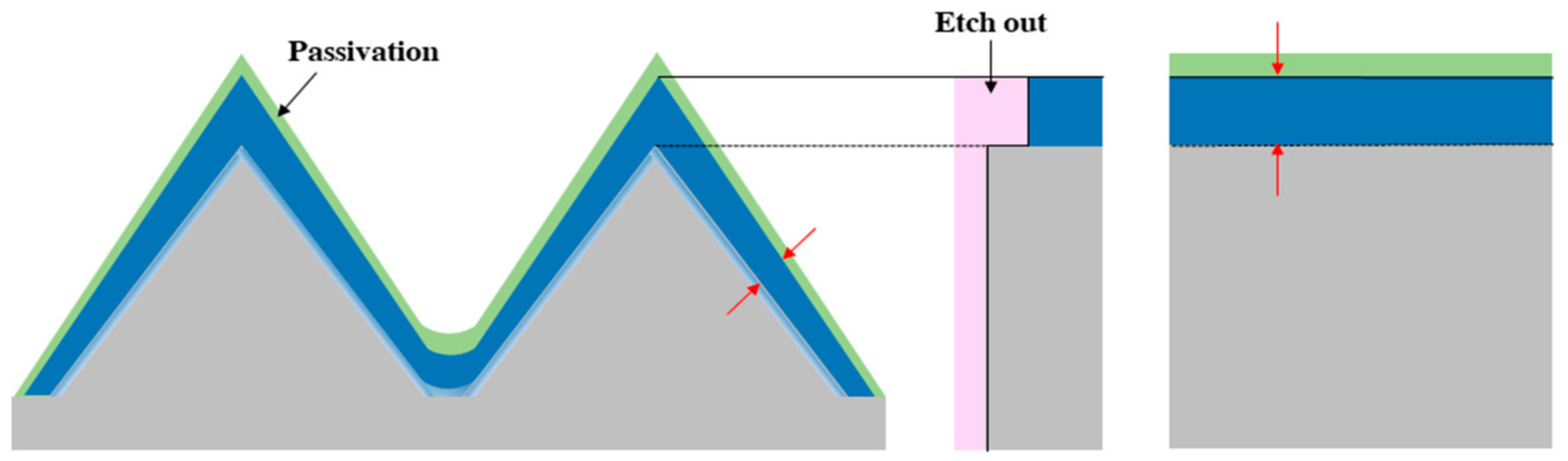
Figure 16 shows a schematic diagram of the selective etching (SE) analysis. The etching solution for SE consisted of HF:HNO3:CH3COOH = 1:100:25, and the doped wafer was etched for 5 s. It is only possible to form an accurate step if there exists a passivation layer on the emitter layer, as this prevents additional etching on the top surface. In this paper, the effect of the pyramid structure on the emitter formation process was analyzed based on the results obtained through the previous experiment.
After the surface etching process, the emitter layer was formed using a furnace. Figure 17 shows a cross-section SEM image of the wafer after the emitter formation process according to various etching process methods. The SEM image is the result of the formation of the n-type emitter and clearly shows the emitter formation structure according to the pyramid structure. Figure 17a is a result of observing the emitter layer formed on the micro-sized pyramid wafer, where it can be seen that a uniform doped layer is formed. In the nano-sized pyramid wafers of Figure 17b–e, it can be observed that the emitter layer has a non-uniform formation compared to the micro-sized pyramid structure. This is judged by the influence of the dopant in the deposition step and the diffusion depth in the diffusion step during emitter formation, and can be explained through a schematic diagram of the formation process of the emitter layer, as shown in Figure 18. To form an emitter on the surface-textured wafer, POCl3 and O2 are injected into the furnace and deposited through pre-deposition and post-diffusion steps. The chemical reaction formula for P diffusion using a liquid source is as follows:
4 POCl 3 + 3 O 2     2 P 2 O 5 + 6 Cl 2  
2 P 2 O 5 + 5 Si     4 P + 5 SiO 2
POCl3 and O2 gas react in a chamber at a high temperature of approximately 800 °C to form a P2O5 layer on the wafer surface. This step is called the pre-deposition step. In this state, when high-temperature heat treatment is performed, the P atoms of P2O5 diffuse to the Si surface to form an emitter layer. This step is called the post-diffusion step. At this time, the dopant deposited on the wafer surface and the diffusion of the P is greatly influenced by the pyramidal structure of the wafer. In the case of a micro-sized pyramid structured wafer, as shown in Figure 18a, the thickness of the top and valley portions of the PSG layer is different. This is because the PSG layer is deposited thinly on the top portion of the pyramid structure due to the tensile properties present. In the valley portions of the pyramid structure, a thick PSG layer is deposited due to the compressive properties present. The thicker PSG layer forms a higher P surface concentration, and a deeper emitter layer is formed in the post-diffusion process. In the case of a micro-sized pyramid, it was observed that the side of the pyramid and the valley portion could form an emitter layer of similar thickness, and the top portion had more diffusion of the dopant and the emitter layer was thicker. In the case of a wafer having a nano-sized pyramid structure as shown in Figure 18b, more valley area is occupied in comparison to the same area of a micro-sized pyramid structure. Like the micro-sized pyramid, a thicker PSG layer is formed in the valley area with the nano-sized pyramid structure. The nano-sized pyramid structure may have a thicker PSG layer than the micro-sized pyramid structure due to the large number of valleys [27,28]. Accordingly, the emitter layer was formed deeper than the micro-sized pyramid structure in the nano-sized pyramid structure wafer. Based on the non-uniformity of the emitter layer observed through the SE analysis, it can be concluded that the formation of the emitter layer according to the pyramid structure has an effect on the number of tops and valleys compared to the same area.
As a result, although the reflectance of the wafer after the etching process was the lowest in the KOH + MACE process, the quantum efficiency value of the KOH process alone was measured to be higher. This is because the recombination rate is high due to the low sheet resistance by the deep emitter layer of the nano-pyramidal structure. It is also expected to be as a result of the influence of the non-uniform emitter layer in the nano-pyramidal structure. Subsequently, in order to increase the efficiency of the cell, it can be seen that the surface of the nano-pyramid using the one-step etching process is more advantageous when considering the formation of the emitter layer rather than the surface of the micro-pyramid using the two-step etching process.

4. Conclusions

In this paper, pyramid structures of various sizes were formed on wafers through various etching methods. First of all, one-step etching processes were performed by using the alkali solution method, MACE method, and RIE method. Next, two-step etching processes were performed by using the alkali solution + MACE methods and alkali solution + RIE methods. The micro-sized pyramid-structured wafer showed a reflectance of approximately 9.11%, and the nano-sized pyramid-structured wafer showed a low reflectance in the range of approximately 1 to 5%. Accordingly, it was determined that the characteristics of the cell fabricated from the nano-sized pyramid-structured wafer having low reflectance would be higher, but it was confirmed that the quantum efficiency characteristics were higher in the micro-pyramidal-structured wafer. It is believed that this is the influence of the non-uniform formation of the emitter layer. In addition, this is because the sheet resistance is low and the recombination rate is high due to the deep emitter layer having a nano-pyramidal structure. As a result, it was confirmed that the micro-sized pyramid-structured wafer exhibited higher quantum efficiency characteristics due to the influence of the doping layer. A surface texture process with low reflectance is very important for improving efficiency. However, if a process with a uniform doping profile is developed according to the pyramid surface structure, short-wavelength region responsiveness can be improved, which can increase short-circuit current density. In addition, if the cell is fabricated by forming an electrode in consideration of the particle size of the Ag paste according to the pyramid structure, the contact area between the Ag paste particles and the doped wafer surface increases, the fill factor is increased. Thus, it is expected that a high-efficiency cell can be obtained.

Author Contributions

J.E.P. and C.-S.H. are the main authors; writing—original draft preparation and writing—review and editing, J.E.P. and C.-S.H.; investigation, W.S.C.; supervision, D.L. All authors participated in the discussion of the results, reviewed the manuscript, and provided input for editing. All authors have read and agreed to the published version of the manuscript.

Funding

This work was supported by the Korea Electric Power Corporation. (Grant number: R17XA05-1), and the Korea Institute of Energy Technology Evaluation and Planning(KETEP) and the Ministry of Trade, Industry & Energy(MOTIE) of the Republic of Korea (No. 20193020010650).

Institutional Review Board Statement

Not applicable.

Informed Consent Statement

Not applicable.

Data Availability Statement

Not applicable.

Conflicts of Interest

The authors declare no conflict of interest.

References

  1. Snapshot of Global PV Markets 2020; Gaëtan Masson, IEA PVPS Task 1 Operating Agent; Snapshot of Global PV Markets; IEA: Paris, France, 2020; p. 19. ISBN 978-3-906042-94-7.
  2. Lee, S.H. Development of High-Efficiency Silicon Solar Cells for Commercialization. J. Korean Phys. Soc. 2001, 39, 369–373. [Google Scholar]
  3. Paviet-Salomon, B.; Gall, S.; Monna, R.; Manuel, S.; Slaoui, A. Analysis of laser-doped phosphorus emitters. Energy Procedia 2011, 8, 214–219. [Google Scholar] [CrossRef] [Green Version]
  4. Hübner, A.; Aberle, A.G.; Hezel, R. Novel cost-effective bifacial silicon solar cells with 19.4% front and 18.1% rear efficiency. Appl. Phys. Lett. 1997, 70, 1008–1010. [Google Scholar] [CrossRef]
  5. Jiang, F.; Liu, T.; Luo, B.; Tong, J.; Qin, F.; Xiong, S.; Li, Z.; Zhou, Y. A two-terminal perovskite/perovskite tandem solar cell. J. Mater. Chem. A 2016, 4, 1208–1213. [Google Scholar] [CrossRef]
  6. Zhao, D.; Yu, Y.; Wang, C.; Liao, W.; Shrestha, N.; Grice, C.R.; Cimaroli, A.J.; Guan, L.; Ellingson, R.J.; Zhu, K.; et al. Low-bandgap mixed tin–lead iodide perovskite absorbers with long carrier lifetimes for all-perovskite tandem solar cells. Nat. Energy 2017, 2, 17018. [Google Scholar] [CrossRef]
  7. Martin, A. Green, Silicon Solar Cells: Advanced Principles & Practice; Centre for Photovoltaic Devices and Systems: Sydney, Australia, 1995; p. 366. [Google Scholar]
  8. Abdullah, M.F.; Lghoul, M.A.; Naser, H.; Asim, N.; Ahmadi, S.; Yatim, B.; Sopian, K. Research and development efforts on texturization to reduce the optical losses at front surface of silicon solar cell. Renew. Sustain. Energy Rev. 2016, 66, 380–398. [Google Scholar] [CrossRef]
  9. Park, H.; Kwon, S.; Lee, J.S.; Lim, H.J.; Yoon, S.; Kim, D. Improvement on surface texturing of single crystalline silicon for solar cells by saw-damage etching using an acidic solution. Sol. Energy Mater. Sol. Cells 2009, 93, 1773–1778. [Google Scholar] [CrossRef]
  10. Gu, Y.; Xue, C.; Zheng, M. Technologies to reduce optical losses of silicon solar cells. Adv. Mater. Res. 2014, 953–954, 91–94. [Google Scholar] [CrossRef]
  11. Lee, D.B. Anisotropic Etching of Silicon. J. Appl. Phys. 1969, 40, 4569–4574. [Google Scholar] [CrossRef]
  12. Wang, S.; Xu, Z.; Gou, X.; Huang, X.; Zhou, S. Study of Nano Texturing on Multi-crystalline Silicon Solar Cells. IOP Conf. Ser. Earth Environ. Sci. 2020, 453, 1–6. [Google Scholar] [CrossRef] [Green Version]
  13. Oxtoby, D.W. Chemistry: Science of Change, 3rd ed.; Saunders College: Rochester, NY, USA, 1997; p. 1152. [Google Scholar]
  14. Yoo, J. Reactive ion etching (RIE) technique for application in crystalline silicon solar cells. Sol. Energy 2010, 84, 730–734. [Google Scholar] [CrossRef]
  15. Halima, A.F.; Zhang, X.; MacFarlane, D.R. Metal-Free Black Silicon for Solar-powered Hydrogen Generation. Electrochim. Acta 2017, 235, 453–462. [Google Scholar] [CrossRef]
  16. Chartier, C.; Bastide, S.; Lévy-Clément, C. Metal-assisted chemical etching of silicon in HF–H2O2. Electrochim. Acta 2008, 53, 5509–5516. [Google Scholar] [CrossRef]
  17. Unagami, T. Formation Mechanism of Porous Silicon Layer by Anodization in HF Solution. J. Electrochem. Soc. 1980, 127, 476. [Google Scholar] [CrossRef]
  18. Moreno, M.; Murias, D.; Martínez, J.; Reyes-Betanzo, C.; Torres, A.; Ambrosio, R.; Rosales, P.; Roca ICabarrocas, P.; Escobar, M. A comparative study of wet and dry texturing processes of c-Si wafers for the fabrication of solar cells. Sol. Energy 2014, 101, 182–191. [Google Scholar] [CrossRef]
  19. Rosli, S.A.; Aziz, A.A.; Hamid, H.A. Characteristics of RIE SF6/O2/Ar Plasmas on n-Silicon Etching. In Proceedings of the 2006 IEEE International Conference on Semiconductor Electronics, Kuala Lumpur, Malaysia, 29 October–1 December 2006; pp. 851–855. [Google Scholar]
  20. Abdullah, M.F.; Hashim, A.M. Reflectance Characteristics of Silicon Surface Fabricated with the Arrays of Uniform Inverted Pyramid Microstructures in UV-Visible Range. Sains Malays. 2019, 48, 1163–1169. [Google Scholar] [CrossRef]
  21. Li, H.; Kim, K.; Hallam, B.; Hoex, B.; Wenham, S.; Abbott, M. POCl3 diffusion for industrial Si solar cell emitter formation. Front. Energy 2016, 11, 42–51. [Google Scholar] [CrossRef]
  22. Werner, S.; Mourad, S.; Hasan, W.; Wolf, A. Structure and composition of phosphosilicate glass systems formed by POCl3 diffusion. Energy Procedia 2017, 124, 455–463. [Google Scholar] [CrossRef]
  23. Vazsonyi, E.; De Clercq, K.; Einhaus, R.; Van Kerschaver, E.; Said, K.; Poortmans, J.; Szlufcik, J.; Nijs, J. Improved anisotropic etching process for industrial texturing of silicon solar cells. Sol. Energy Mater. Sol. Cells 1999, 57, 179–188. [Google Scholar] [CrossRef]
  24. Abdur-Rahman, E.; Alghoraibi, I.; Alkurdi, H. Effect of Isopropyl Alcohol Concentration and Etching Time on Wet Chemical Anisotropic Etching of Low-Resistivity Crystalline Silicon Wafer. Int. J. Anal. Chem. 2017. [Google Scholar] [CrossRef]
  25. Hsu, C.-H.; Liu, S.-M.; Lien, S.-Y.; Zhang, X.-Y.; Cho, Y.-S.; Huang, Y.-H.; Zhang, S.; Chen, S.-Y.; Zhu, W.-Z. Low Reflection and Low Surface Recombination Rate Nano-Needle Texture Formed by Two-Step Etching for Solar Cells. Nanomaterials 2019, 9, 1392. [Google Scholar] [CrossRef] [PubMed] [Green Version]
  26. Huang, Z.G.; Lin, X.X.; Zeng, Y.; Zhong, S.H.; Song, X.M.; Liu, C.; Yuan, X.; Shen, W.Z. One-step-MACE nano/microstructures for high-efficient large-size multicrystalline Si solar cells. Sol. Energy Mater. Sol. Cells 2015, 143, 302–310. [Google Scholar] [CrossRef]
  27. Voyer, C.; Buettner, T.; Bock, R.; Biro, D.; Preu, R. Microscopic homogeneity of emitters formed on textured silicon using in-line diffusion and phosphoric acid as the dopant source. Sol. Energy Mater. Sol. Cells 2009, 93, 932–935. [Google Scholar] [CrossRef]
  28. Dastgheib-Shirazi, A.; Steyer, M.; Micard, G.; Wagner, H.; Altermatt, P.P.; Hahn, G. Relationships between Diffusion Parameters and Phosphorus Precipitation during the POCl3 Diffusion Process. Energy Procedia 2013, 38, 254–262. [Google Scholar] [CrossRef] [Green Version]
Figure 1. The path of light incident on the V-shaped surface according to angle.
Energies 14 04106 g001
Figure 2. Cross-sectional SEM images of the c-Si wafer before and after the SDR process: (a) c-Si wafer before the SDR process, (b) c-Si wafer after the SDR process, and (c) reflectance of the c-Si wafer before and after the SDR process.
Energies 14 04106 g002
Figure 3. Characteristics of the wafer according to the KOH and IPA concentrations: (a) etching depth and (b) reflectance.
Energies 14 04106 g003
Figure 4. SEM images of wafer surface according to KOH and IPA concentrations: (a) KOH 2 wt.%, IPA 7.5 vol.%; (b) KOH 2 wt.%, IPA 9 vol.%; (c) KOH 3 wt.%, IPA 7.5 vol.%; and (d) KOH 3 wt.%, IPA 9 vol.%.
Energies 14 04106 g004
Figure 5. Reflectance and cross-section SEM images of wafer surfaces according to etching times for the MACE process: (a) 30 s, (b) 90 s, (c) 180 s, (d) 270 s, and (e) 360 s.
Energies 14 04106 g005
Figure 6. Reflectance and cross-section SEM images of wafer surfaces according to mole fraction ( ρ ) for the MACE process: (a) ρ 50%, (b) ρ 60%, (c) ρ 70%, (d) ρ 80%, (e) ρ 90%, and (f) ρ 100%.
Energies 14 04106 g006
Figure 7. Reflectance and cross-section SEM images of wafer surfaces according to gas ratio for the RIE process: (a) SF6:O2 = 5:1, (b) SF6:O2 = 4:1, (c) SF6:O2 = 3:1, (d) SF6:O2 = 2:1, (e) SF6:O2 = 1:1, and (f) SF6:O2 = 1:2.
Energies 14 04106 g007
Figure 8. Reflectance and cross-section SEM images of wafer surfaces according to etching time for the RIE process: (a) 200 s, (b) 300 s, (c) 400 s, (d) 500 s, (e) 600 s, and (f) 700 s.
Energies 14 04106 g008
Figure 9. Reflectance and cross-section SEM images of wafer surfaces according to ρ for the two-step etching process with alkali solution and MACE: (a)   ρ 50%, (b) ρ 16.6%, and (c) ρ 9.09%.
Energies 14 04106 g009
Figure 10. Reflectance and cross-section SEM images of wafer surfaces according to etching time for the two-step etching process with alkali solution and MACE after depositing a Ag metal catalyst according to various thicknesses: (a) 1 min, (b) 2 min, (c) 3 min, (d) 4 min, and (e) 5 min.
Energies 14 04106 g010
Figure 11. Energy dispersive X-ray spectroscopy (EDS) measurement results before and after removing Ag particles.
Energies 14 04106 g011
Figure 12. Reflectance and cross-section SEM images of wafer surfaces according to gas ratio for the two-step etching process with alkali solution and RIE: (a) SF6:O2 = 3:1, (b) SF6:O2 = 2:1, (c) SF6:O2 = 1:1, (d) SF6:O2 = 1:2, and (e) SF6:O2 = 1:3.
Energies 14 04106 g012
Figure 13. Reflectance and cross-section SEM images of wafer surfaces according to RF power for the two-step etching process with alkali solution and RIE: (a) 25 W, (b) 50 W, (c) 75 W, (d) 125 W, (e) 150 W, and (f) 200 W.
Energies 14 04106 g013
Figure 14. Reflectance characteristics and pyramid size according to various etching process methods: (a) reflectance with etching process methods in the wavelength range of 400~1000 nm and (b) a comparison of reflectance when different etching process methods were utilized.
Energies 14 04106 g014
Figure 15. Quantum efficiency characteristics according to various etching process methods: (a) external and (b) internal.
Energies 14 04106 g015
Figure 16. Schematic diagram of selective etching (SE) analysis.
Energies 14 04106 g016
Figure 17. Cross-section SEM images of wafer after emitter formation process according to various etching process methods: (a) Alkali solution, (b) MACE, (c) RIE, (d) Alkali solution+MACE, (e) Alkali solution+RIE.
Energies 14 04106 g017
Figure 18. Schematic diagram of the emitter formation process according to pyramid size: (a) Micro-sized pyramid, (b) Nano-sized pyramid.
Energies 14 04106 g018
Publisher’s Note: MDPI stays neutral with regard to jurisdictional claims in published maps and institutional affiliations.

