Abstract
In this paper, a predictive model is developed to characterize the impact of high-frequency electromagnetic interference (EMI) on the leakage current of CMOS integrated circuits. It is shown that the frequency dependence can be easily described by a transfer function that depends only on a few dominant parasitic elements. The developed analytical model is successfully compared against measurement data from devices fabricated using 180 nm, 130 nm, and 65 nm standard CMOS processes through TSMC. Based on the predictive model, the impact of EMI on leakage current in a CMOS inverter is reduced by increasing the frequency from 10 MHz to 4 GHz.
1. Introduction
Power dissipation in electronics has always been one of the major concerns of the massive growth in portable computing and wireless communication technologies. The exponential relationship between power consumption and the square of the power supply voltage has led to the scaling down of CMOS transistors to reduce dynamic power draw and offset reliability issues [1,2]. Transistor threshold voltages are also reduced to maintain a high drive current and achieve performance improvements [3]. However, these measures result in an exponential increase in leakage current when the transistor’s size is in the nanometer range. Consequently, leakage current becomes a significant portion of CMOS circuit’s total power consumption [4]. Although enormous efforts have been made to mitigate leakage current, such as MTCMOS Power Gating, Super Cutoff CMOS Circuitry, Forced Transistor Stacking, and Sleepy Stack techniques [5], the design of such leakage-free nanoscale CMOS circuits turns out to be very challenging.
Moreover, as the device size enters the nanometer scale and the bias voltage is reduced, the integrated circuits and systems become more vulnerable to EMI [6,7]. A low level of electromagnetic coupling from an external EMI source can still disrupt the operation of a circuit by causing soft, reversible upset, or hard, permanent damage, even when numerous techniques for reducing the effect of EMI are implemented, such as shielding and filtering of the digital modules and power supplies [8,9]. Although the modeling of the EMI susceptibility of digital circuits related to delay time and power supply current [10], or upset of CMOS inverters in static operation [11], is recently attracting attention, there is no model to predict the impact of EMI on the leakage current.
Leakage or static power dissipation occurs due to the presence of various leakage currents, such as subthreshold leakage, reverse-bias source/drain junction leakages, gate oxide tunneling leakage, and Gate-Induced Drain Leakage (GIDL). Because subthreshold leakage current is the dominant leakage in sub-100 nm circuits [12], we focus on evaluating the said current’s changes when an RF signal is injected onto the gates of CMOS inverters, which are the fundamental units in electronic ICs and systems.
Subthreshold leakage is the drain-source current of a transistor during operation in the weak inversion regime. Unlike the strong inversion regime, in which drift current dominates, subthreshold conduction is due to the diffusion current of the minority carriers in the channel for a metal oxide semiconductor (MOS) device. The magnitude of the subthreshold current is a function of temperature, supply voltage, device size, and the process parameters [13,14]. A CMOS device comprises both PMOS and NMOS transistors; therefore, its leakage current will be determined based on which MOSFET is in the OFF state.
In our previous work, we reported on a predictive model to estimate the impact of EMI on the leakage current of a digital integrated circuit at the low frequency of 10 MHz [15]. Based on our developed predictive model, we found that the rate of increase in leakage current, as a function of injected RF power, is independent of transistor scaling, technology node, or power supply voltage.
This paper’s main contribution is to extend our predictive, analytical model to higher frequencies, focusing on elemental CMOS inverters. Our predictive model for the device’s leakage current under such high frequency injected interference is validated with experimental results.
The remainder of this paper is organized as follows: In Section 2, the high-frequency model of the leakage current under EMI is established and the main factors that affect the leakage current are discussed. Section 3 presents the experimental setup and the test chip prototype. The measured results and comparisons are shown in Section 4. Finally, we conclude by summarizing the key results uncovered through this research.
2. Predictive Model for Leakage Current under EMI
In this section, we develop an analytic model to predict the inverter’s leakage susceptibility as a function of the frequency and power of the injected EMI. Our initial experiments and research have focused on large-signal injection at a low frequency of 10 MHz, where the impact of parasitic device capacitances was negligible [16,17]. Figure 1a depicts the leakage current of a CMOS inverter with and without RF injection at its input terminal. In an inverter, the leakage current will be determined with the transistor in the OFF state. For example, if the applied voltage to the gate is zero and the NMOS is OFF, the leakage current is due to the NMOS; however, if the applied voltage to the gate is set to VDD, then the PMOS is OFF, and the leakage current is due to the PMOS. In both cases, leakage current appears due to diffusion between the source and the drain of MOSFET and can be calculated using the following expression [18]:
where Ioff is the OFF state current, VGS is the gate-source voltage, VDS is the drain-source voltage, VT = KT/q is the thermal potential (≈25 mV at room temperature), and n is the subthreshold swing coefficient.
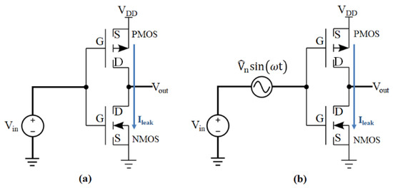
Figure 1.
Leakage current of a CMOS inverter in standby mode (a) with (b) without RF injection.
Since VGS voltage is zero, VDS can be estimated by the power supply voltage, VDD. Therefore, by substituting VGS = and VDS ≈ VDD in Equation (1), the leakage current under EMI over one cycle of the RF injection , and knowing VDD ≫ VT will yield (see [15])
where I0 is the modified Bessel function of order zero.
Our previous study revealed that leakage current is very sensitive to EMI at low frequency, where only a few hundred millivolts of noise can increase the leakage current by a factor of 1000. However, here we must consider the effect of parasitic loading and capacitance of the test circuit by extraneous instrumentation devices because of high RF frequency injection. Therefore, to further investigate the correlation between RF injection and leakage current, a deeper study of the “transfer function” is required. Here, we propose modeling the frequency response of the device under test (DUT) using assumptions and approximations that will be substantiated by comparing to experimental data.
2.1. Assumptions
One of the basic assumptions of experiments with RF injection is that the characteristic impedance of the system’s transmission line is 50 Ω. Although the injected EMI can be applied to any inverter terminal, we assume the excitation is fed to the input, which is typically the most sensitive terminal of the device and, in many practical applications, the most likely input of the RF signal [19].
2.2. Predictive Model
The basic building block in CMOS digital logic devices is the inverter. Although the inverter in different series and parallel configurations is used in logic topologies, a single inverter stage is analyzed here for ease of analysis. Moreover, to achieve precise control of the coupled voltage characteristic at the device input, we apply an RF signal directly onto inverter pins using microwave probes. Because the parasitic impedances have a more significant influence on device performance, the model developed here explores high- frequency injection, where the parasitic impedances arise in the inverter, transmission line, and source.
2.3. Transfer Function
The cascaded combination of frequency-varying transfer functions of the system, coupling to cables, and component susceptibility often means that the total transfer function from the incident field to the malfunction of an internal component shows a significant variation as a function of frequency. As shown in Figure 2, the transfer function is responsible for defining the peak injection received by the input of the inverter. The transfer function is given by:
where is the phasor showing the level of RF signal coupling into input of device and is the voltage of the RF source, which can take several forms depending on the physical property of the cables, connectors, probes, or DUT. The effective voltage then is
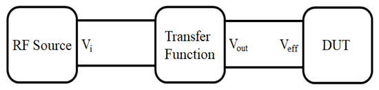
Figure 2.
Schematic of the voltage transfer function.
Here, because we use the precision ground-signal-ground (G-S-G) probes for RF signal injection, the dominant elements of the equivalent circuit will be the parasitic resistance of the RF source, the transmission line (Z0), and substrate (Rsub), and the parasitic capacitance of the pad (Cpad), as shown in Figure 3.
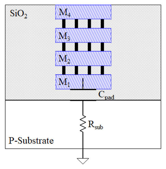
Figure 3.
Cross-section of the pad capacitance and substrate resistance.
2.4. Pad Capacitance
Although the device size has reduced substantially in advanced CMOS technology, the contact metal size still needs to be relatively large to ensure bonding reliability. As a result, the pad capacitance cannot be decreased by scaling the CMOS technology. Therefore, in most RF applications, the pad capacitance is considered part of the matching network. The cross-sectional view of the pad capacitance is depicted in Figure 3. The first plate is formed using M4, M3, M2, and M1, which are Ohmic contacts and connected through a via. It is worth mentioning that different metals (or alloys) are used to decrease the Schottky barrier height and, therefore, the contact resistance. The oxide layer SiO2 between plates 1 and 2, which is a p-type substrate (P-Substrate), can be used as an insulating dielectric between the parallel plates. Therefore, using a metallic parallel-plate model, the pad capacitance is given by:
where ϵr, and d are the relative permittivity and thickness of the insulator, respectively, ϵ0 is the permittivity of free space, and A is the area that will be determined from the smaller areas of plates 1 and 2, which in this case is the area of the M1. The area of M1 on a fabricated test chip is 150 µm × 360 µm, and the relative permittivity of SiO2 is 3.9. Therefore, the value of pad capacitance, which is determined by the thickness of the oxide layer, will be in the range of 2 pF to 8 pF.
2.5. Substrate Resistance
The bottom plate of the pad capacitor is the silicon substrate, which introduces some Ohmic resistance to the ground terminal depending on its doping concentration. At high frequency, this substrate resistance, which is typically around 20 to 30 Ω, must be taken into consideration. In this circuit model, the substrate resistance (Rsub) is the resistance between the pad capacitor and the reference ground terminal.
2.6. Frequency Response of Equivalent Circuit
According to the equivalent circuit (Figure 4), the peak injection received by the input of the inverter can be calculated as:
where XC is the pad capacitor impedance is Xc = 1/(jωCpad), and jw = s. Therefore:
and:
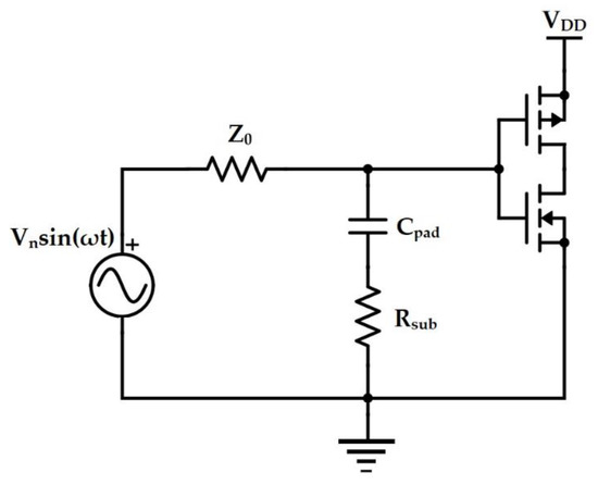
Figure 4.
Simplified schematic of the experimental test circuit showing Z0, Cpad, and Rsub.
The zeros and poles of the system are defined as the roots of the numerator and the denominator of the transfer function, respectively. According to Equation (8), the zeros and poles of the system will be at frequencies f0 and fp, respectively, given by:
The voltage transfer functions of 180 nm, 130 nm, and 65 nm technologies relative to frequency are calculated and plotted in Figure 5. This is analogous to the insertion loss typically determined from the S11, but easier to experimentally obtain given the high impedance of the gate inputs, which is not conducive for S-parameter measurements with a Vector Network Analyzer. Table 1 shows the physical properties and cutoff (−3 dBm) frequencies of the fabricated devices.
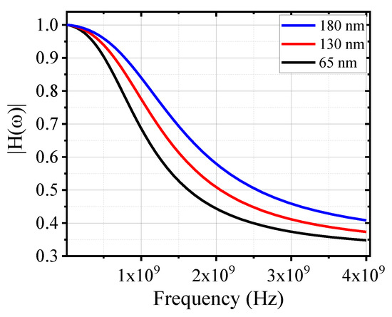
Figure 5.
Voltage transfer versus frequency.

Table 1.
Cutoff frequencies of 180 nm, 130 nm, and 65 nm technology node.
This model’s advantage is its ability to calculate the frequency response of leakage current using a transfer function for the circuit. The transfer function can be varied according to the measurement setup, fabrication process, and dominant elements at high frequency. The leakage current is given by:
Note that the transfer function can be developed for any other applications depending on the test setup. Typically, 50 Ohms matching termination cannot be implemented in digital applications, where the gate input is high impedance. Therefore, in practical digital circuits, the transfer function will be dependent on the interconnect capacitance/resistance as well as the substrate resistance. The presented methodology is a guide for designers to generate their own transfer function depending on their test setup.
3. Experimental Setup and Methodology
To understand the impact of EMI on leakage current and compare the experimental data with the developed predictive model, several test chips were designed and fabricated using various TSMC’s standard CMOS technology nodes, including 180 nm, 130 nm, and 65 nm. To investigate the effects of EMI on leakage current, measurements both with and without microwave injection are performed on a test chip at the input of 1X INV using G_S_G probes having a 350-µm pitch on a coplanar probe station. A photograph of the test chip under the probes is shown in Figure 6. The three RF probes provide Vin, VDD, and GND connections for the 1× inverter on the test chip, respectively. The RF probes have three pins with ground-signal-ground configuration, as shown in Figure 6.
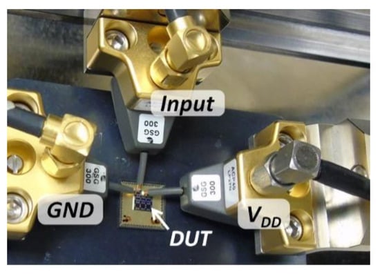
Figure 6.
Photograph of the test chip and the RF probes setup used in the measurements [15].
A RF signal generator (Keysight, Santa Rosa, CA, USA) is used to excite the input of the 1× inverter. To measure the leakage current due to NMOS, the inverter input is not biased (no dc gate voltage); however, for leakage current of PMOS, DC voltage and RF signal are injected onto the input using a bias tee. The carrier frequency ranges from 10 MHz to 4 GHz, and the input signal amplitude is set to less than the threshold voltage to satisfy leakage current condition. The leakage current is measured using a Keithley semiconductor analyzer with fixed VDD, and a controlled RF signal injected onto the device’s input.
The experimental setup is shown in Figure 7. The entire system in our experimental setup is controlled via LabView (National Instruments, Austin, TX, USA), where the voltages and RF injection power are parametrically swept, and the device leakage current is measured and stored. To avoid exciting photocurrents, all measurements are performed in a darkened room. Figure 8 and Figure 9 show the dependence of leakage current on the RF power and frequency based on measurement data of 180 nm, 130 nm, and 65 nm technology. As expected, the leakage current of the inverter increases as the amplitude of RF signal increases; however, this change is smaller at high frequencies.
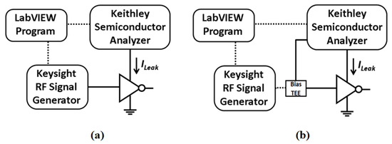
Figure 7.
The block diagram of the experimental setup with the LabVIEW control program, measuring leakage current of (a) NMOS; (b) PMOS.
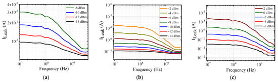
Figure 8.
The measured leakage current due to a NMOS for a 1× inverter fabricated in the (a) 65nm, (b) 130 nm, and (c) 180 nm standard CMOS technology node.
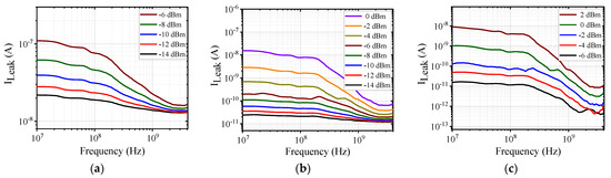
Figure 9.
The measured leakage current due to a PMOS for a 1× inverter fabricated in the (a) 65nm, (b) 130 nm, and (c) 180 nm standard CMOS technology node.
Since power is an important priority in the design of submicron technology in an integrated circuit, the increase of leakage current of the inverter due to EMI could result in serious disruption in the total power budget distribution of the entire system [20]. Therefore, the entire integrated circuit may experience logic failure. In addition, at higher power injection, leakage current is more sensitive to the change in the peak power of the interference. At fixed RF power, leakage current decreases by increasing RF frequency from 10 MHz to 4 GHz. RF power effects are strongly suppressed at frequencies above 1.2 GHz. This indicates that the inverter is more susceptible to EMI at the low-frequency range.
After the RF injection event, the devices are measured again in order to determine whether there were permanent changes in their operating characteristics. No permanent damage was observed. Therefore, these effects should be considered as ‘‘soft’’ error effects where the device can return to its normal operation without permanent damage; however, they are able to decrease the battery life of the device.
4. Comparison of Predictive Model with Measured Data
To validate the accuracy of the proposed predictive model, the analytical model is compared against measured data from the fabricated test chips using TSMC’s 180 nm, 130 nm, and 65 nm standard CMOS processes. Figure 10 and Figure 11 depict the calculated effective voltage that gets injected into the input of the inverter using Equation (8). Figure 12 and Figure 13 illustrate the predictive model in solid line and the normalized leakage currents (ILeak/Ioff) of PMOS and NMOS.
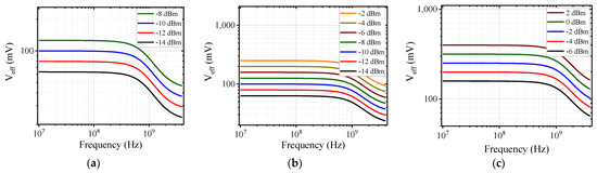
Figure 10.
Calculated Veff for NMOS in the inverter (a) 65nm, (b) 130 nm, and (c) 180 nm technology node.
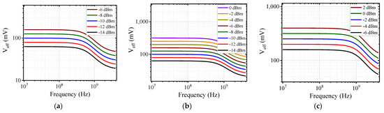
Figure 11.
Calculated Veff for PMOS in the inverter (a) 65nm, (b) 130 nm, and (c) 180 nm technology node.
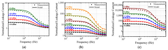
Figure 12.
Comparison between the analytical model and the measured data for leakage current of NMOS for (a) 65 nm, (b) 130 nm, and (c) 180 nm technology node.
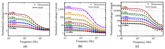
Figure 13.
Comparison between the analytical model and the measured data for leakage current of PMOS for (a) 65 nm, (b) 130 nm, and (c) 180 nm technology node.
The leakage current of the devices under investigation is measured based on the electrical system shown in Figure 7. Then the measured leakage current at different powers is fitted to the model with fit parameters of Ioff, n, Cpad, and Rsub. Ioff and n are responsible only for defining the initial point. Cpad and Rsub are the parameters of the transfer function that are dominant in determining the trend of model at high frequency. Cpad is the dominant fitting parameter for the middle range of frequency, while Rsub adds a zero to the transfer function and plays the main role in frequencies higher than 1 GHz. The pertinent device parameters are extracted by comparing the measurements to the model and given in Table 2.
Table 2.
Transistor sizes and parameters.
In general, the model, to first-order, predicts the values and behavior of the measured leakage current of devices. At low frequencies around 10 MHz, the model predicts a small slope in the change of leakage current, which measurements also confirm that leakage current is a weak function of applied RF frequency in the low frequency regime. In the high frequency range, the model predicts the change in the slope of leakage current, while there is a mismatch in the absolute values of Ileak at some frequencies and powers.
The purpose of our research is to generate simple rule-of-thumb guidelines for MOS design engineers who have to design their products to operate in extreme EM environments. While we acknowledge the “quantitative” mismatch between the model and data, for reasons cited above, these parasitic aspects can be characterized and can lead to system-specific EM susceptibility curves. However, the general trend in the data is still captured by our simple and elegant model thereby paving the way for a quick assessment of damage thresholds in MOS circuits, where there are billions of transistors in a single chip.
5. Conclusions
To the best of our knowledge there has not been any previous predictive model for leakage current under EMI. Our previously published model captures the leakage model only at low frequencies [15]. The new predictive model presented in this paper extends our previous model by taking frequency into consideration. The model uses only a few primitive device and system parameters to successfully predict the behavior of EMI injection on the leakage current in a CMOS inverter over a wide range of frequencies up to 4 GHz. Although the model is developed for a CMOS inverter, it can also be applied to any other complex logic gates using the leakage current of the equivalent transistor in the logic gate. The developed analytical model is successfully compared against measurement data for devices fabricated using 180 nm, 130 nm, and 65 nm standard CMOS process through TSMC. This simple model can be utilized by EMI/EMC engineers to quickly ascertain the soft and hard error decision limits for their circuits under external RF interference.
Author Contributions
Conceptualization, T.A., P.Z.-H.; developing the model, P.Z.-H., Z.A.; collecting and analyzing measured data, Z.A.; writing—original draft preparation Z.A.; writing—review and editing, S.H., E.S., P.Z.-H.; supervision, S.H., E.S., P.Z.-H. All authors have read and agreed to the published version of the manuscript.
Funding
This research is funded by United States Air Force Research Laboratory (AFRL) and Air Force Office of Scientific Research (AFSOR) with AFOSR/AFRL COE Grant #FA9550-15-1-0171 and by DURIP Grant #FA9550-15-1-0379.
Data Availability Statement
Not applicable.
Conflicts of Interest
The authors declare no conflict of interest.
References
- Lakshmi Narayanan, S.; Korah, R.; Swarnalatha, A. Novel 10-T Write Driver SRAM Design Using 45 nm CMOS Technology with Leakage Current Reduction Scheme for FPGA Routing Switch Architecture. J. Nanoelectron. Optoelectron. 2017, 12, 1–13. [Google Scholar]
- Friedman, E.G.; Kursun, V. Node Voltage Dependent Subthreshold Leakage Current Characteristics of Dynamic Circuits. In Proceedings of the International Symposium on Signals, Circuits and Systems, San Jose, CA, USA, 22–24 March 2003. [Google Scholar]
- Roy, K.; Mukhopadhyay, S.; Mahmoodi-Meimand, H. Leakage Current Mechanisms and Leakage Reduction Techniques in Deep-Submicrometer CMOS Circuits. Proc. IEEE 2003, 91, 305–327. [Google Scholar] [CrossRef]
- Ho, Y.; Hsu, C. Standby Power Reduction Using Dynamic Standby Control with Voltage Keeper. IEICE Electron. 2017, 1–7. [Google Scholar] [CrossRef]
- Priya, M.G.; Baskaran, K.; Krishnaveni, D. Leakage Power Reduction Techniques in Deep Submicron Technologies for VLSI Applications. Procedia Eng. 2012, 30, 1163–1170. [Google Scholar] [CrossRef]
- Kim, K.; Iliadis, A.A. Impact of Microwave Interference on Dynamic Operation and Power Dissipation of CMOS Inverters. IEEE Trans Electromagn Compat. 2007, 49, 329–338. [Google Scholar] [CrossRef]
- Deepaksubramanyan, B.S.; Nu˜nez, A. Analysis of Subthreshold Leakage Reduction in CMOS Digital Circuits. In Proceedings of the 50th Midwest Symposium on Circuits and Systems, Montreal, QC, Canada, 5–8 August 2007. [Google Scholar]
- Ferchau, J.U.; Kotyuk, K.A.; Diaz, R.J. Electronic Assembly with Improved Grounding and EMI Shielding. U.S. Patent No. 5,311,408, 10 May 1994. [Google Scholar]
- Lee, S.; Jeong, S.; Hong, S.; Sim, B.; Kim, J. Design and Analysis of EMI Shielding Method using Intermediate Coil for Train WPT System. In Proceedings of the Wireless Power Transfer Conference (WPTC), Montreal, QC, Canada, 3–7 June 2018. [Google Scholar]
- Hwang, S.; Hong, J.; Han, S.; Huh, C.; Huh, U.; Choi, J. Delay time and power supply current characteristics of CMOS inverter broken by intentional high power microwave. In Proceedings of the Microwave Conference, Bangkok, Thailand, 11–14 December 2007. [Google Scholar]
- Kim, K.; Iliadis, A. Critical Upsets of CMOS Inverters in Static Operation Due to High-Power Microwave Interference. IEEE T Electromagn C 2007, 49, 876–885. [Google Scholar] [CrossRef]
- Abraham, D.; George, A. Effect of Fin Shape on GIDL and Subthreshold Leakage Currents. Int. J. Sci. Eng. Technol. 2015, 1, 135–145. [Google Scholar]
- Nandyala, V.R.; Mahapatra, K.K. A Circuit Technique for Leakage Power Reduction in CMOS VLSI Circuits. In Proceedings of the International Conference on VLSI Systems, Bengaluru, India, 10–12 January 2016. [Google Scholar]
- Roy, K.; Mukhopadhyay, S.; Mahmoodi-Meimand, H. Leakage Current in Deep-Submicron CMOS Circuits. J. Circuits Syst. Comp. 2002, 11, 575–600. [Google Scholar] [CrossRef]
- Abedi, Z.; Hemmady, S.; Antonsen, T.; Schamiloglu, E.; Zarkesh-Ha, P. Electromagnetic Compatibility in Leakage Current of CMOS Integrated Circuits. In Proceedings of the International Symposium on Electromagnetic Compatibility (EMC EUROPE), Barcelona, Spain, 2–6 September 2019. [Google Scholar]
- Sule, N.H.; Abedi, Z.; Hemmady, S.; Schamiloglu, E.; Zarkesh-Ha, P. Predictive Modeling for Estimating the Limits for Nonpersistent Effects in MOSFET Response Under Large Signal Gate Injection. IEEE T Electromagn C 2020, 62, 1763–1770. [Google Scholar] [CrossRef]
- Powell, T.; Sule, N.; Hemmady, S.; Zarkesh-Ha, P. Predictive Model for Extreme Electromagnetic Interference on CMOS Inverters. In Proceedings of the International Symposium on Electromagnetic Compatibility (EMC EUROPE), Amsterdam, The Netherlands, 27–30 August 2018. [Google Scholar]
- Sheu, B.J.; Scharfetter, D.L.; Ko, P.; Jeng, M.C. BSIM: Berkeley Short-Channel IGFET Model for MOS Transistors. IEEE J. Solid State Circuits 1987, 22, 558–566. [Google Scholar] [CrossRef]
- Tadano, H.; Hattori, Y. A Study of DC Operating Point Shifts in MOSFETs with Large RF Signals. Electron. Commun. Jpn. I Commun. 2001, 84, 18–26. [Google Scholar]
- Sengupta, D.; Saleh, R. Generalized Power-Delay Metrics in Deep Submicron CMOS Designs. IEEE Trans. CAD 2007, 26, 183–189. [Google Scholar] [CrossRef]
Publisher’s Note: MDPI stays neutral with regard to jurisdictional claims in published maps and institutional affiliations. |
© 2021 by the authors. Licensee MDPI, Basel, Switzerland. This article is an open access article distributed under the terms and conditions of the Creative Commons Attribution (CC BY) license (https://creativecommons.org/licenses/by/4.0/).