Review

The Challenge for Building Integration of Highly Transparent Photovoltaics and Photoelectrochromic Devices

by
Alessandro Cannavale
1,2,*,
Francesco Martellotta
1,
Francesco Fiorito
3 and
Ubaldo Ayr
1
1
Department of Sciences in Civil Engineering and Architecture, Polytechnic University of Bari, 70125 Bari, Italy
2
Istituto di Nanotecnologia, CNR Nanotec, Via Arnesano 16, 73100 Lecce, Italy
3
Department of Civil, Environmental, Land, Building Engineering and Chemistry, Polytechnic University of Bari, 70125 Bari, Italy
*
Author to whom correspondence should be addressed.
Energies 2020, 13(8), 1929; https://doi.org/10.3390/en13081929
Submission received: 19 March 2020 / Revised: 9 April 2020 / Accepted: 10 April 2020 / Published: 14 April 2020
(This article belongs to the Special Issue Low and Zero Energy Highly Performing Buildings)

Abstract

:
This paper holds a critical review of current research activities dealing with smart architectural glazing worldwide. Hereafter, the main trends are analyzed and critically reported, with open issues, challenges, and opportunities, providing an accurate description of technological evolution of devices in time. This manuscript deals with some well-known, highly performing technologies, such as semitransparent photovoltaics and novel photoelectrochromic devices, the readiest, probably, to reach the final stage of development, to disclose the manifold advantages of multifunctional, smart glazing. The complex, overall effects of their building integration are also reported, especially regarding energy balance and indoor visual comfort in buildings.

1. Introduction

The progressive exhaustion of fossil fuels and the consequent biosphere alteration are strictly related to the dramatic growth of energy consumption. Global warming witnesses the effects of anthropic activities on the biosphere. In 2015, during the Conference of Paris, representatives of 196 countries agreed on the urgency to reduce the impacts of human activities [1]. In 2016, fossil fuels still provided 87% of global energy supply with renewable energies reaching a 10% share [2].
These issues invoke the development of novel, environmental-friendly technologies, exploiting renewable energy sources, since the rate of energy consumption is by far smaller than the incoming solar power, which is about 90 PW [2,3]. The need to reduce energy consumption and to develop new, less energy-intensive technologies, and also the need to use more and more renewable resources, is largely motivated if one considers that the constructions require approximately 40% of the primary energy yearly used in the European continent [4]. Such a huge energy consumption is especially due to Heating, Ventilation, Air Conditioning (HVAC) and lighting in buildings. Pichot et al. [5] reported that, in the USA, cooling accounts for 10% to 15% of electric energy consumption.
Even in an evolved technological framework, like the one of developed countries, architectural glazing still acts as a thermal weak point, allowing for undesired heat gains in summer and relevant thermal losses in winter, thus affecting the energy efficiency of architectural envelopes. Therefore, a real “Holy Grail” for designers of building envelopes could be represented by smart, multifunctional devices that are capable of dynamically tuning their thermo-physical figures of merit, according to perceived changes of environmental parameters. Semitransparent photovoltaic (PV) glazing, as well as smart windows, belong to the emerging classes of multifunctional “skins” for energy efficient buildings [6,7,8]. These technologies have attracted researchers worldwide, as they could be pivotal in the design of innovative, multifunctional building facades.
In this review paper, newly developed PV materials are reported, with the potential to create market opportunities for the building integration of photovoltaics (BIPVs) [9,10], with special reference to the recent design of solution processable PV devices, which is bringing new impulse to the spread of PV glazing. On the other hand, smart windows [11], mainly employing electrochromic (EC) materials [12], are attractive for their capability to reversibly modulate visible and near infrared (NIR) transmittance, according to precise variations of external stimuli. This allows for visual interaction with the environment, effective glare and illuminance control, but also thermal comfort management, affecting energy supply and potential saving, as largely demonstrated [13,14,15]. Smart windows are considered to be a promising technology worldwide, indeed expected to play a relevant role as an architectural component in future buildings [16], by optimizing daylighting use as well as cooling demand, mainly depending on their use strategy [17,18]. Thus, the dynamic behavior of glazing can be the natural evolution of novel PV devices towards “intelligent building skins”.
In this compelling roadmap, photoelectrochromic devices (PECDs), allowing for chromic transition, like common smart windows already on market, might be relevant players, since they would not need any external electric power source to work: in fact, they are capable of exploiting the available sun irradiance to generate electric energy by internal PV conversion and are capable of responsively modulating their transmittance [19,20,21].

2. Novel Technologies for Glazing: A Useful Glossary

The development of new materials to be used in constructions requires the accurate check of their real usability. This requires the early, accurate measurement of the performance of new materials and devices, the assessment of the figures of merit describing such performance, well before the technology development reaches its final stage; this also allows for design and performance correction, before the end of the experimental development activities. To this end, the synergy between development and computer simulation activities becomes a relevant step to lead the full exploitation of new technologies, in certain areas of the planet. It is widely accepted that BIPVs need to overcome various barriers consisting in cost-efficiency considerations, but also aspects concerning psychological and social factors [22], still acting as limiting factors for their spread. Nevertheless, they will play a role in the design of zero energy buildings (ZEBs) in the near future: to this aim, BIPVs will have to successfully comply with aesthetical, economic, and technical constraints before being considered to be fully suitable for integration in envelopes, since the early stages of design [23,24], being ready to fulfil the multiple requirements of BIPVs, acting as multifunctional building components [25,26,27]. Quite predictably, most relevant candidates for BIPV are those devices showing high transparency in the visible range of wavelengths, which is the main figure for architectural glazing.
High transparency in BIPVs is probably the main figure of merit, because it allows for an increase of the surface of building envelopes that are engaged in energy harvesting, providing a supplementary contribution to energy generation (apart from rooftops and opaque surfaces), but also to provide multiple features, like shading or even dynamic shading, so as to maximize (or optimize) daylighting use. The parameter allowing for quantifying this attitude is the visible transmittance (Tvis), also named light transmittance, provided by the following expression [28]:
T v i s = 380 n m 780   n m T ( λ ) D λ V ( λ ) Δ λ 380 n m 780   n m D λ V ( λ ) Δ λ
where Dλ is defined as relative spectral features of a D65 illuminant, V(λ) is the spectral luminous efficiency for photopic vision of a standard observer, T(λ) is the monochromatic transmittance of the glass in the visible range (between 380 nm and 780 nm) and Δλ is the wavelength interval. On the other hand, solar transmittance (Tsol), including the contribution of infra-red radiation, is given by the following expression [28]:
T s o l = 300 n m 2500   n m T ( λ ) S λ Δ λ 300 n m 2500   n m S λ Δ λ
with Sλ representing the relative spectral distribution of solar radiation. Δλ is the wavelength interval and T(λ) is the monochromatic transmittance of the glass, between 300 nm and 2500 nm.
Moreover, average visible transmittance (AVT) is often adopted as a measure of the mean visible transmittance, between 380 nm and 780 nm [29]. Transparency in glazing is indeed a pivotal feature and minimum acceptable values exist for AVT. A specific study by Boyce et al. [30] reported the threshold of minimum acceptable transmittance for glazing in office buildings, ideally falling within the range 25–38%. This is a fundamental parameter for both semitransparent PVs and the bleached state of PECDs. Moreover, a specific survey showed that effective smart glazing for building integration should switch their Tvis from 50–70% in the bleached state, down to less than 10–20% in the coloured state [31]. With these premises, one can observe that most of the ECs and PECDs have reported compatible values of transmittance, with reference to both the lower and the upper thresholds [32].
A relevant measure of these variations is the contrast ratio (CR), expressed by:
C R = T b T c
where Tb represents transmittance in the bleached state and Tc is in the colored state. Transmittance (or absorbance) modulation can be expressed in terms of modulation: ΔT% (or ΔA%). The modulation kinetics of chromogenic materials and devices can be expressed in terms of response time (expressed in s), i.e., the time that is required to complete the transition between (bleached/colored) states. In some cases, it expresses the time to activate a given fraction of the complete modulation, expressed by the time constant. Response time is generally measured at a specific wavelength.
Another relevant parameter, frequently used in order to analyze performance of chromogenics, is the coloration efficiency (CE), which measures the modulation of optical density per unit of intercalated charge. The change in optical density (ΔOD), depending on the contrast ratio, is first expressed, at each wavelength, by:
Δ O D = l n T b ( λ ) T c ( λ )
where Tb(λ) and Tc(λ) represent, respectively, the monochromatic transmittance in the bleaced and colored states, respectively. Then, CE is generally calculated at the wavelength showing maximum absorbance as a function of charge density (Q/A), and can be expressed as follows:
C E = Δ O D Q / A = l n T b ( λ ) T c ( λ ) Q / A  
A high value of CE is an index of a large contrast activated using a small amount of charge extraction and insertion. This parameter is generally adopted in EC devices, in which Q/A is provided by an external circuitry.
When PECDs are considered, a more suitable figure of merit, substantially equivalent to CE, is represented by photo-coloration efficiency (PhCE), when considering the different way to provide charge insertion in such devices, generally exploiting PV conversion to be activated. In this case, the exposure energy is considered, that is the irradiance times the exposure time.
P h C E = Δ O D I · t
Let I represent the light reaching the device (W/m2) and t the exposure time (min).
Moreover, open circuit memory represents the time in which coloration remains unvaried, without requiring any bias to restore the desired coloration stage. For this reason, this figure represents an asset for chromogenics because, in devices with large open circuit memory, additional power will be necessary only to obtain small changes in the optical properties. Devices showing small drifts of the optical state, after several hours, are by far preferred.

3. Novel Technologies for Semitransparent PVs

The first strategy adopted to increase cell transparency, in order to obtain semitransparent solar cells, was to spatially segment opaque silicon (Si) cells or copper indium gallium selenide (CIGS) cells, dispersing cells across a transparent substrate, so as to allow for the optical transmission of light through free spaces between cells, aiming at a good compromise between energy harvesting and indoor visual comfort. This happened especially for technologies belonging to first (and second) generation PVs. Since then, improvements have been achieved, which involve different technologies, including dye-sensitized solar cells (DSSCs), amorphous silicon (a-Si) cells, organic cells, and solid-state heterojunction solar cells. Unfortunately, none of them has still gained the expected role in market share [33,34,35,36,37,38]. A huge, multidisciplinary research effort would be required to foster a coherent development of technologies for semitransparent BIPVs. Tailor-made materials for solar cells should be characterized by low cost, should be reliable and efficient as systems now on the market, and be durable and stable, as required by regulations, with pleasant aesthetics and high transparency, to be really considered to be suitable for glazing use. Lightweight, flexible—or even rollable—solar cells could easily find their place in the emerging BIPV sector [39].

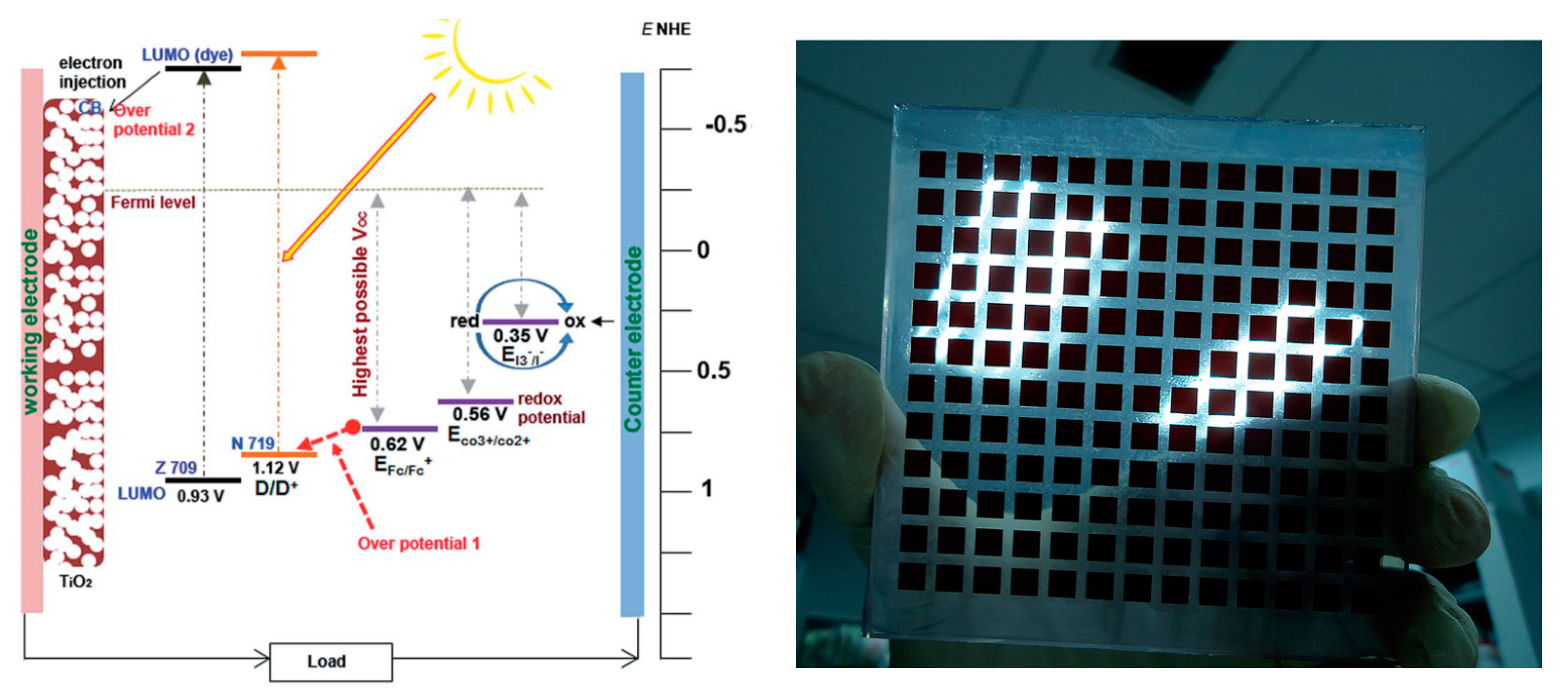
3.1. Dye Sensitized Solar Cells (DSSCs)

DSSCs, also known, worldwide, as Grätzel solar cells, contain a photoelectrode embodying a mesoporous semiconductor oxide (generally, titanium dioxide (TiO2), but also Zinc oxide), sensitized by means of metalorganic or fully organic dyes, influencing light absorption according to their properties [40]. N719 is the commercial name of the most used ruthenium-based dye, showing its effectiveness along the visible spectrum; it achieves conversion efficiencies (η) that span from 7% exposed to standard test conditions, to about 11% in diffuse daylighting conditions [26]. Several ruthenium complexes—like N3, N719, N749–and black dyes have been designed and synthesized. These dyes acted as paradigms for highly efficient charge-transfer, though they show some inherent drawbacks, like high cost, complex, and costly synthesis, and the use of limited amounts of noble metals [41].
For this reason, metal-free organic dyes have been proposed to replace ruthenium-based dyes. Lee et al. [42] reviewed several suitable organic materials for photoanodes, electrolytes, and metal-free catalysts, reporting efficiencies that exceed 5%. Their degree of transparency and colour can be tuned according to the photoanode properties (thickness and crystalline phase) and to the dyes adopted. Parisi et al. [43] carried out a Life-Cycle Approach (LCA) analysis to compare DSSCs to other PV technologies. The former showed better results.
The suitability of semi-transparent DSSCs for integration in glazing was investigated by Selvaraj et al. [44], who found that 37% transparent DSSCs may break down the phenomenon of disturbing glare by 21%, as compared to a clear double glazed unit, in the same conditions.
As reported by Fakharuddin et al. [45], DSSC panels might even outperform their silicon and thin film cells counterparts in delivering electricity when exposed to low irradiance (Figure 1).
Kitamura et al. investigated the relevant issue of DSSCs’ durability [46], who found how to mitigate the effect of water intrusion into the electrolyte, employing ionic liquid electrolytes, eventually enhancing stability of cells. This solution ensured high stability of PV performance, even at high temperatures, and those DSSCs successfully passed the Japanese standards tests for endurance of a-Si PVs (JIS C 8938). Other durability limitations may be induced by solvent evaporation and electrolyte leakage, due to inefficient device sealing. Reale et al. [47] developed a model to study a building integrated PV system embodying DSSC technology, starting from experimental data measured on modules operating in outdoor conditions. The semitransparent DSSC module presented in this work embodied 13 cells, connected while adopting a “Z” layout. N719 dye on semitransparent TiO2 layers were used for modules with a surface area of 16 × 17 cm2. Real data that were collected outdoor were used to calculate the producible energy in real locations using available weather data. DSSCs outperformed c-Si, a-Si, CdTe, and CIGS, well established technologies for BIPV applications, after normalizing the energy production with the peak energy production. This point, according to the authors, was due to the better behavior in the diffuse light conditions of DSSCs respect to other PV technologies. Their performance was better than standard technologies in any possible orientation.

3.2. Amorphous Silicon Solar Cells and Thin Film Solar Cells

Among the different PV technologies that are potentially available for their semitransparency, even though their appearance is basically brownish, a-Si cells are typically thinner than other first (and second) generation technologies (c-Si, mainly, or CdTe, CdSe, or CIGS solar cells). [48]. a-Si cells typically undergo initial efficiency decay due to the Staebler–Wronski effect, which reduces efficiency due to de-passivation under light soaking [49]. a-Si tiles could be used on rooftops, but also semi-transparent modules have been reported as suitable solutions for façades or glass ceilings, effectively allowing for light penetration indoor [50,51]. PV systems’ transparency can be enhanced by reducing the thickness of PV materials, though at the expenses of photovoltaic conversion efficiency. Chae et al. [52] studied building-integrated semitransparent a-Si solar cells with a 120-nm-thick a-Si:H absorber, showing η = 4.8%, with visible transmittance reaching 0.27. The dependence of electric performance on the changing absorption properties of devices is reported in Figure 2. They found that BIPVs in glazing reduces the yearly energy consumption for HVAC and greenhouse gas emission thanks to the PV electricity generation, but also to their thermal and optical features. The energy generation ranged from 22 kWh/myr to 45 kWh/myr per year using a-Si:H cells. These data were mainly influenced by type of PV cell, location, and façade orientation.

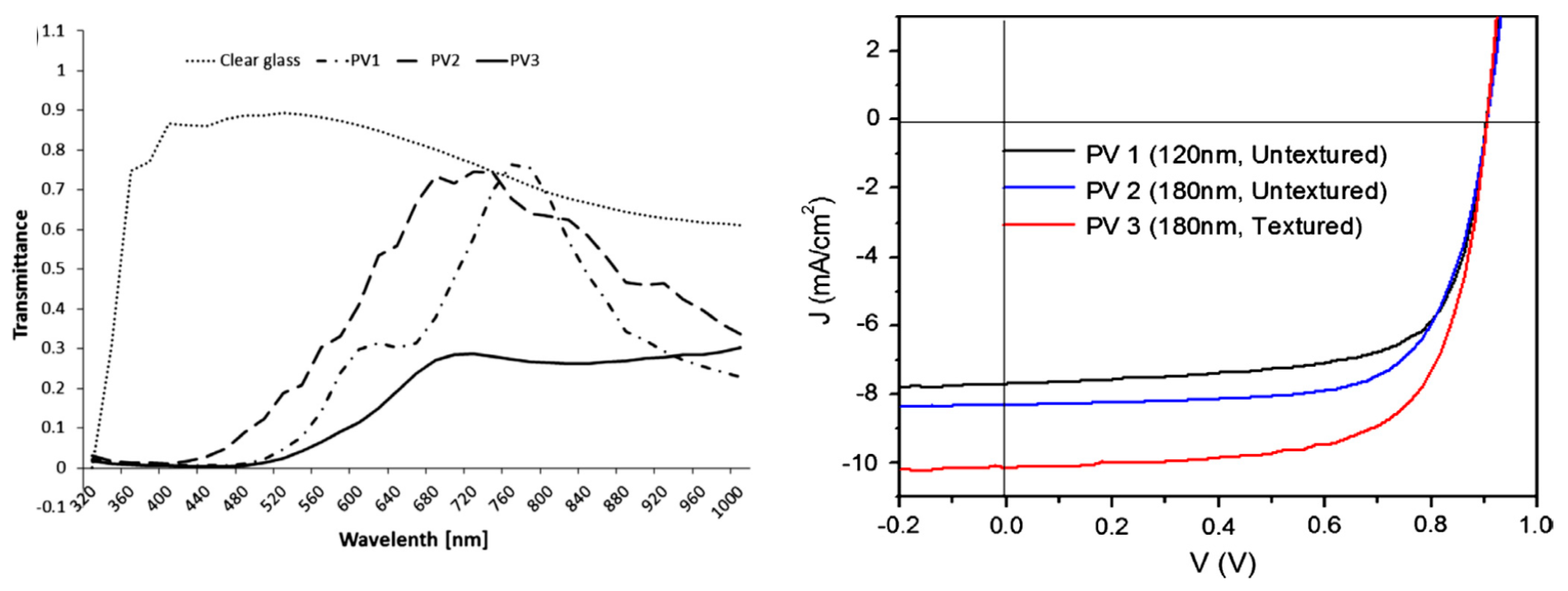
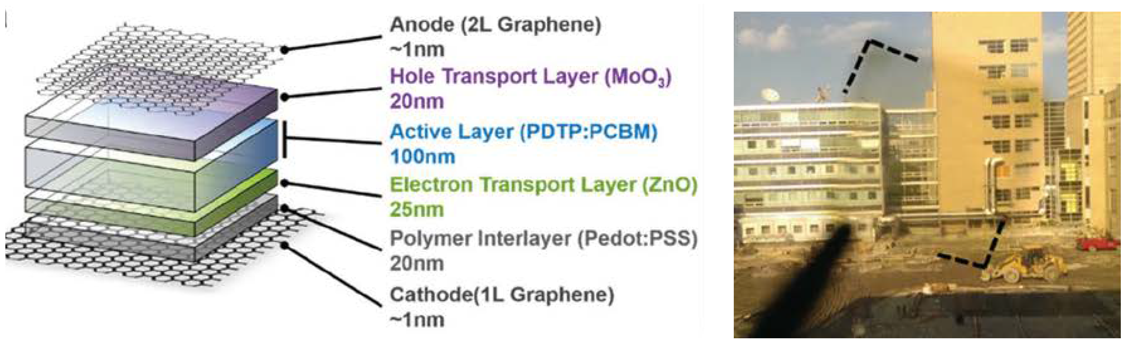
3.3. Organic Solar Cells

The so-called organic PVs (OPVs), as reported by Krebs et al. [53], can be manufactured using abundant materials, in very thin devices, with an overall thickness of about 100 nm, being susceptible for continuous and cheap printing/coating processes, starting from liquid ink. Transparency in OPVs is once again a compromise between film deposition parameters and captured photons, low resistance, and suitable optical properties. OPVs embody organic layers replacing metals and metal oxides in the role of effective electron/hole transporting layers in a device. Chen et al. [54], report some solution-processable materials, like carbon nanotubes and graphene, replacing transparent conductive oxides, or PEDOT:PSS. In their work, a blend of PBDTT-DPP and PBDTT-PCBM acted as photoactive layers with complementary absorption. These devices reached efficiencies higher than 5%. All of these layers are generally sandwiched between a 100 nm thick metal cathode (or silver nanowires) and a transparent conductive oxide about 150 nm thick [55,56]. The great interest in OPVs worldwide is mainly due to their lightness, semitransparency, and flexibility, which make them quite unique among the innovative power generation technologies. Song et al. recently reported optical transmittance up to 69% (550 nm) [37]: they combined very transparent graphene electrodes with NIR/UV-absorbing organic polymers (Figure 3). Conversion efficiency between 2.8% and 3.8% was achieved for these flexible devices. Kim et al. [39] reported efficiencies of 5–6% for all-polymer solar cells, opening the way to further enhancement.

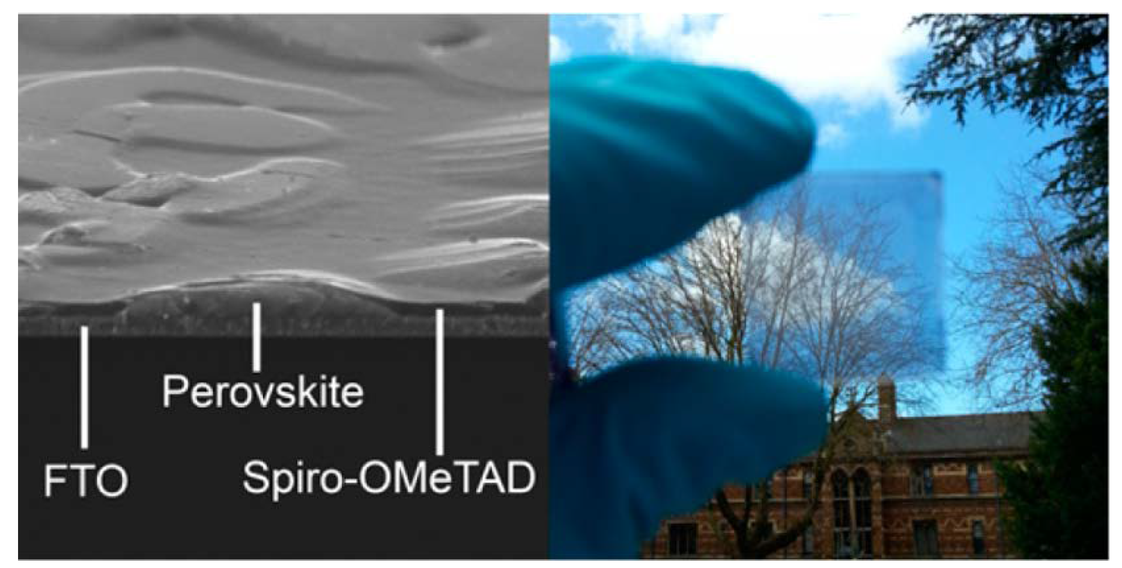
3.4. Perovskite-Based Heterojunction Solar Cells

A new generation organic–inorganic hybrid two-dimensional (2D) perovskite semiconductors was developed since the first decade of the new millennium, as reported by Zhang et al. [57]. Green et al. [58] showed the extremely rapid progress of perovskite-based PVs, since 2012. Kim et al. [59] reported a mesoscopic solar cell embodying heterojunction structure and nanoparticles of methyl ammonium iodide as efficient light absorbers, being infiltrated on TiO2 mesoscopic films. These cells contained Spiro-MeOTAD, acting as a hole conductor and reported large current densities (17 mA/cm2) and conversion efficiency of 9.7%. In a couple of years, the efficiency overcame 15% and perovskite-based cells had proven to be interesting candidates for their potentially low-cost solution-processable fabrication [60,61]. Additionally, devices with compact TiO2 layers and tandem architectures were reported, obtaining efficiency exceeding 20% [62]. This solid-state PV technology has shown an impressive increase of conversion efficiency, reaching 16.2% at the end of 2013 and recently achieving η = 25.2%, at a laboratory scale, as testified by the most recent NREL chart [63].
More than 13300 papers were published from 2012 to august 2019 on perovskite solar cells, according to a recent review by Park et al. [64]. Such paper described active research toward the scale-up of perovskite-based cells and modules. Encouraging efficiencies of 17.3% were measured on devices with surface area of 17.277 cm2 and of 11.7% for devices of 203 cm2.
Perovskite-based solar cells offer interesting prospects due to high energy conversion efficiencies and low processing costs. Perovskites are well-known materials with structural formula ABX3, (X an anion, A and B are cations, with the former larger than B). Toxicity issues in fabrication, deployment, and disposal of devices were raised about perovskites, due to the embodied lead used in some synthetises. Lead-free perovskites have been proposed and disposal issues are currently under study. It should be highlighted that research on perovskites for PVs is at the very early-stage, when compared to other consolidated technologies [65].
Other relevant open issues are represented by stability and degradation, mainly due to moisture. Christians et al. [66] have studied the degradation mechanisms observed in perovskites. Their modified device architecture retained more than 94% of its best performance, after undergoing 1000 hr of accelerated degradation testing, even without sealing; the tests consisted in continuous illumination in ambient humid air. More test activities will be a necessary further step to prove that perovskite-based cells could work for at least 20 years; nevertheless, this result is a relevant benchmark, showing the potential improvements that were achievable by this emerging technology. The most interesting aspect of this new class of solid-state heterojunction solar cells certainly lies in the entirely new opportunity to greatly simplify the design of the device, paving the way to building integration. These cells have very low overall thickness, of a few microns, and they are fully compatible with glazing industrial processes. Another interesting aspect, which is currently under investigation, is represented by costs of perovskite-based PVs. The cost of perovskite cells has been calculated and it was estimated to be about 40 USD/m2, much less than the cost of silicon solar cells [67]. Furthermore, Song et al. [68] have calculated the minimum sustainable price and manufacturing cost of those innovative cells, finding a value of 31.7 ± 5.5 $/m2. On the other hand, processing costs (24.9 ± 4.3 USD/m2) resulted lower comparing perovskite-based cells to previously diffused thin film technologies (29 US$/m2 for CIGS and 27 USD/m2 for CdTe cells). Tunable aesthetics can be an asset for newly designed perovskite-based PVs. In fact, the colour of perovskite cells can be suitably customized by tuning cations used in the basic perovskite structure [69]. Zhang et al. [70] proposed a photonic approach to improve and customize aesthetics in perovskite cells. They followed the natural route to obtain structural colours by means of photonic crystals, as observed in butterfly wings; they created a scaffold within the photoactive layer, so as to tune the color of the solar cell across the visible spectrum, adopting a bottom-up approach, aiming to a scalable, cheap liquid processing technique. In this way, different colours in perovskite cells were obtained, employing the interference of scattered light waves.
A non-uniform solution deposition of perovskite layers was exploited to fabricate semi-transparent cells based on perovskites. This approach was demonstrated by Eperon et al. [29] who found that the de-wetting of films can be suitably leveraged to obtain micro-structured arrays of perovskite “islands”. These islands effectively absorbed all visible light without covering the whole surface (Figure 4). The resulting “de-wet” regions were fully transparent. The average transmittance was associated to a neutral-coloured, highly semitransparent film, avoiding the brownish tint that is typical of thin semiconductors; this process has proven to be a potentially low-cost approach towards the fabrication of large area solar cells. Micro-islands can be tuned in order to achieve different covering ratio on the substrate. Their thickness, of about 1 μm, allows them to fully absorb all light at energies exceeding their band gap, which is 1.55 eV, though keeping high transparency of the full film containing, due to the presence of large uncovered residual surface. Moreover, the color-neutrality of these PV films was assessed by means of the 1931 xy colour space (by the Commission Internationale de l’Eclairage (CIE)) and colour perception indices were reported.
This novel approach succeeded in forming semitransparent and neutral-coloured solar cells with efficiencies that approached 8%, being observed at the lowest transmittances, i.e., AVT ∼7%. On the contrary, cells showing higher transparency, showed AVT of ∼30% and efficiencies of 4.5% (open circuit voltage ∼0.7 V).
Horäntner et al. [71] observed that this process produces shunting paths in the “de-wet” island morphology, resulting in an undesired contact between electron and hole transporting layers, by-passing the photo-active micro-islands. This produced a reduction of photocurrent density. The resulting “shunt paths” reduce the shunt resistance and also the fill factor parameter. Horantner et al. coped with it by selectively filling the uncovered regions by means of an insulating material, i.e., octadecyl-siloxane molecules, acting as selective electronic insulating barriers; in fact, they attached to the exposed surface of compact TiO2, without affecting charge transport in the perovskite islands. Thanks to this behavior of octadecyl-siloxane in the device architecture, they obtained an increase in conversion efficiency up to 6.1% for neutral coloured semitransparent perovskite cells, with a really high device AVT, reaching approximately 40%.
Aharon et al. [72] reported a different method for obtaining highly transparent perovskite solar cells, depositing CH3NH3PbI3 (MAPbI3) perovskite, exploiting the film formation enabled by a screen printing mesh. These cells, with AVT spanning from 19% to 67%, reported conversion efficiencies of 4.98% and 0.38%, respectively.
Quiroz et al. also reported two alternative protocols for semitransparent perovskite films [73], resulting in a Tvis of 37% and a conversion efficiency (η) of 7.8%. They also commented that fast growing efficiencies of perovskite solar cells in the latest years, low temperature process, and the use of cheap raw materials make them promising candidates to be a pivotal PV technology in the future. Chang et al. analysed production costs for perovskite modules, though at an early stage of technology development [60]. They explained that this emerging technology should exceed CdTe efficiency of 20% and also lifetime, to be really competitive.

3.5. Open issues for Building Integration of Semi-Transparent PVs

The building integration of PVs raises several issues, including visual comfort features, the amount of harvested energy, the optimisation of indoor sunlight penetration, and the effect on the use of artificial lighting sources for lighting. BIPVs is not only relevant in terms of yearly energy balance, but it also affects the attainable level of indoor visual comfort, if windows, skylights or canopies are equipped with PV systems [74,75]. To effectively replace common glazing, solar cells, even if embedded and sealed in laminated glazing, should reach threshold values of average transmittance. Only in this case, the building element could be considered to be compatible with the multiple issues for integration in transparent facades. Nevertheless, Kapsis et al. [76], comparing a-Si, Polycrystalline-Si and thin film organic solar cells, demonstrated that in cooling dominated climates, semi-transparent PVs with 10% transmittance reported the best results in terms of end-use electricity savings and that the optical figures of modules were highly sensitive on the criteria adopted for daylight and lighting control. Zomer et al. investigated the difficult balance between aesthetic requirements and performance in building integrated silicon-based cells [77]. a-Si solar cells were reported as a suitable technological choice for BIPV, in works by Chae et al. [52] (η = 4.80%, Tvis = 0.30) and by Lim et al. (η = 5.93%, Tvis = 0.18) [78].
Olivieri et al. [9] analysed the impact of building integrated semi-transparent PV cells on HVAC and lighting loads; they also considered electricity generation. Window to wall ratio (WWR) and cells AVT (with Tvis ranging from 0% to 40%) were the main parameters adopted. They found that semi-transparent solar cells could provide yearly energy saving between 18% (WWR = 33%) and 59% (WWR = 88%), respectively, as compared to clear glass.
As seen in previous sections, a-Si cells report better performance (at low irradiance levels) than perovskite semitransparent cells. However, perovskite-based cells outperformed a-Si cells when their performance was analysed under a more holistic perspective [79], because of two main reasons: their exceeding conversion efficiencies as well as for their favourable optical properties (their neutral-colour results in a substantially grey glass, whereas a-Si cells appear orange or brownish, since they absorb blue-green radiation). Recently, a systematic, parametric approach was adopted to consider multiple figures of merit to study the manifold effects that could derive from building integration of semitransparent perovskite cells [80]. It was demonstrated that those cells, apart from producing electric energy, may also perform as an effective solar control film, shielding undesired solar gains, providing higher levels of indoor visual comfort, as well as energy saving. Daylight metrics, such as Useful Daylight Illuminance (UDI) [81,82] and Daylight Glare Probability (DGP) [83], were adopted in order to estimate the effects of perovskite cells on visual comfort, in the framework of a suitably designed test room. Three sites were chosen for the analyses based on their different climatic characteristics. As to glare probability, the use of PV glazing significantly lowered the DGP hours in all cases. In the office case, PV glass reduced the number of working hours with high occurrence of glare probability down to 16%, 23%, and 12% in London, Brindisi, and Aswan, respectively. The yearly energy yielding due to BIPVs was found to be at least comparable to the annual electric expenditures for artificial lighting.
The potential benefits deriving from perovskite-based BIPVs were determined for a real office building in Bari, Italy [84,85]. Building-integrated semi-transparent perovskite cells reduced the total “passive” energy balance by 4% due to their inherent shielding behavior. “Passive” means that PVs are considered as not operating. On the other hand, if considered as operating, semitransparent perovskite glazing reduced the energy uses by 15% on a yearly basis. The addition of further horizontal PV shades to PV glazing reduced the energy yield of the PV glazing, but, when combined to the above-mentioned passive benefits, resulted in a 22% energy reduction, compared to the reference case. Meanwhile, using such devices proved to be an effective strategy to control over illuminance and glare problems.
Another important point, affecting BIPVs, relates to cost. As reported by Jelle [86], a maximum acceptable payback time of 10 years for PV modules is expected in Europe and it is generally achieved with Statal subsidies. A desirable reduction of PV cost might pave the way towards attractive solutions of high integration. Yang and Zou [74] discussed benefits and existing barriers to the commercial spread of BIPVs. The main benefits could be: the reduction of carbon emissions and social costs, lower environmental impact of constructions, reduced land use as compared to the first stage of PV spread, and lower electricity bills for building users. Ideally, BIPV components in architectural envelopes may produce a sort of mere cost-offset, when compared to traditional elements, both in new construction and in energy retrofit: according to Benemann et al. [10], silicon cells caused an additional offset-cost of about 350–500 USD/m2 when compared with a standard glass façade. A paper by Attoye et al. [87] explained that an appropriate BIPV customization might help in overcoming several BIPV persisting barriers to their adoption, such as aesthetics, architectural integration, and lower performance.

4. The Architectural Evolution of Chromogenics for Building Integration

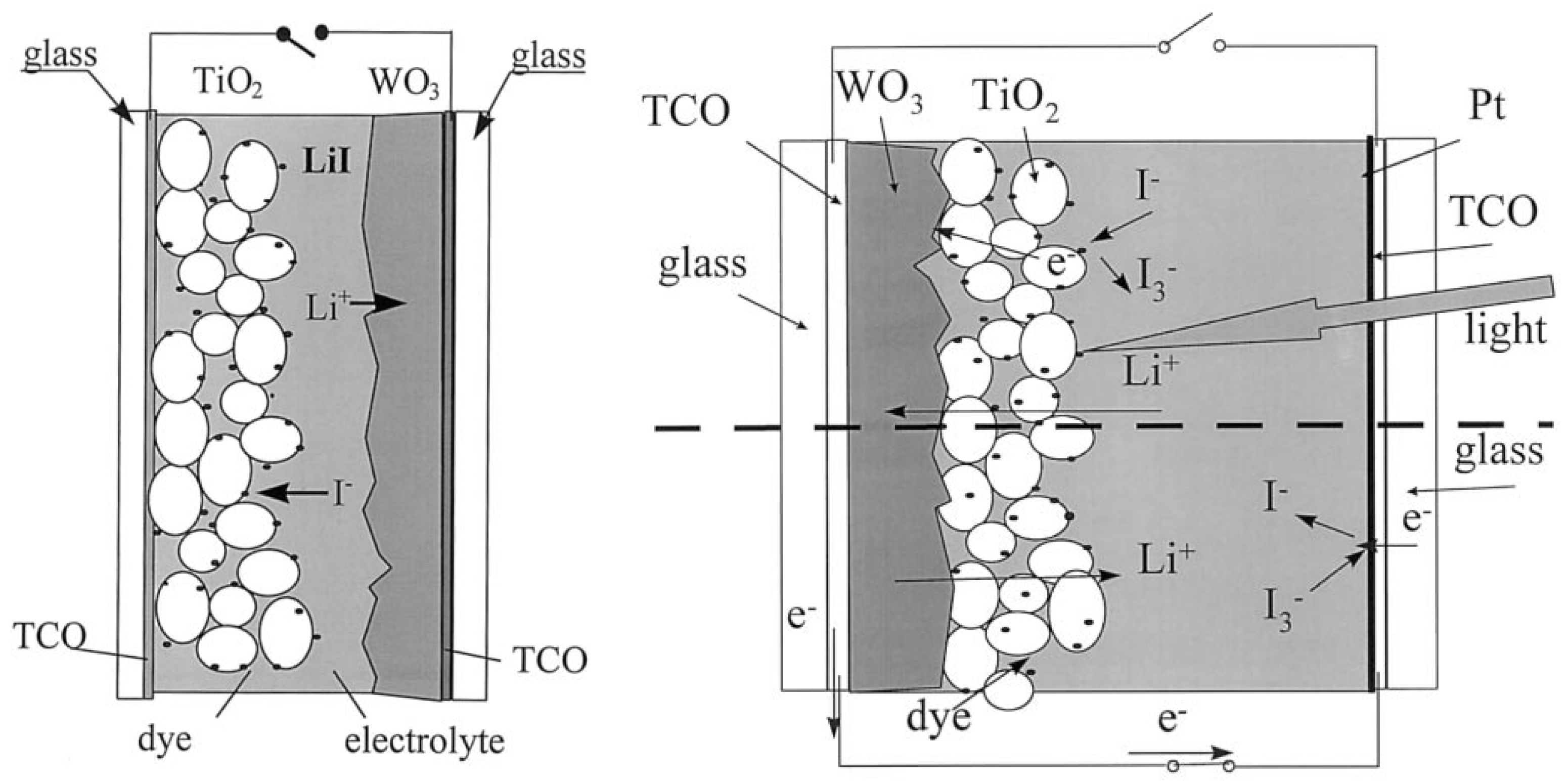
4.1. A chronological Review of PECDs

The first publication reporting electro-optical measurements of PECDs [19] dates back to 1996 and it was hailed as an intriguing fusion of two different technologies: smart windows and PVs. This new class of devices was, in fact, capable of sensing changes in light irradiation to produce consequent responses in modulation of transmittance, paving the way towards the design of smart building skins [32]. Since they can produce electric energy by means of PV conversion like a common solar cell, the dynamic “self-modulating” capability was not only self-powered, but also calibrated according the electric output, thus providing a modulation potentially dependent on the variable environmental conditions. Given this premise, as we will show hereafter, PECDs would positively affect the building energy balance, reducing energy consumption for cooling and electric lighting. Several architectures have appeared since that first disclosure of PECDs in literature, compelling researchers to classify the systems to simplify their analyses.
As reported elsewhere [32], PECDs may be conveniently grouped according to several criteria, including: EC materials used, the PV technology activating the observed chromogenic behavior, the arrangement of layers within the device layout, but also the mutual arrangement of EC and PV layers, operation mode (available external circuit, mechanism of coloration activated in open-circuit, or in short-circuit conditions), the materials’ state of aggregation within the device architecture (solid, liquid, gel) or the manageability of the device by users, to control its features.
The ideal criterion to analyse PECDs’ evolution in time might be the chronological one: in fact, this approach shows the impact of materials’ evolution on the technological development of PECDs, clearly showing occurring trends in the design of devices and materials. The main influencing factor has been represented so far by the PV technology adopted, in turn affecting the efficiency and durability of PECDs. Differently from photochromic films, this PECD embodied a PV film on its photoanode, being completely separated from the cathodic EC material, by means of a liquid electrolyte: the device hosted a dye-sensitized TiO2 (light absorber) on the photoelectrode and a tungsten trioxide (WO3) layer, deposited on the counter electrode. When irradiated, electrons that were generated on the photoanode moved into the WO3 film (photovoltage in open circuit was about 0.6–0.9 V) via an external circuit, reaching tungsten sites. Subsequently, lithium ions were attracted from the electrolyte. This process allowed for a reversible redox reaction standing at the basis of the coloration process. Later, B. Gregg [21] lowered the iodine content in the electrolyte, in order to maximize the cell photovoltage. Moreover, he opted for a more transparent dye in order to reduce the device absorbance.
Since then, PECDs have attracted strong interest among researchers without achieving, so far, a real market entry, probably due to the deceiving expectations of technologies in the field of BIPVs. Afterwards, Li et al. [88] proposed another “separated’’ PECD architecture, employing polyaniline (PANI) as anodic EC material. In separated PECDs, the materials involved in PV generation and those in charge for coloration stand on separated electrode. In this case, the photo-generated voltage allowed for a fair de-coloration of the anodic electrochromic PANI layer. Pichot et al. [5] fabricated the first PECD on flexible polymer substrates, with a low temperature process of TiO2 films. A turning point was represented by Hauch’s architecture [89]: in this case, the TiO2 layer was deposited onto the WO3 layer, with EC and PV materials sharing the same substrate in a so-called “combined” architecture (Figure 5). Full coloration took place under illumination (open-circuit), with a tcol of about 2 min., (for both colouring and bleaching). The kinetics was accelerated due to the thin platinum (Pt) catalyst layer, being deposited on the counter electrode. This PECD colours if illuminated at open circuit, because the photogenerated electrons pass from TiO2 to WO3. Once electrons diffuse in the EC material, they attract lithium ions, giving coloration; on the contrary, the device bleaches if short-circuited, because electrons use the circuitry to reach the counter-electrode; this activates regeneration of iodine ions available inside the electrolyte as well as the concomitant deintercalation of lithium from WO3, resulting in a bleaching. Liao et al. [90] adopted PEDOT as a cathodic EC, measuring ΔT of 20–22% at 630 nm. Krasovec et al. [91] fabricated a solid-state PECD while using a solid lithium-based ion conductor and an organically modified silane containing a typical iodine/iodide redox couple. In this stable architecture (highly stable, after 50 days), the colouring process took place under open-circuit conditions, if exposed to sunlight, reaching an optical modulation of 60% under irradiation. The solid-state electrolyte affected the kinetics, which was slower when compared to PECDs containing liquid electrolytes.
Georg et al. also demonstrated a solid-state electrolyte, with high open-circuit memory (up to 100 h) [92]; the solid state of the electrolyte undoubtedly affected the slower coloration kinetics (15 min.). For the first time in PECDs’ studies, a current-voltage characteristic curve was reported, envisaging, at last, the challenging idea to employ PECDs for smart solar control as well as PV conversion (η was, anyway, as low as 0.054%). Nokki et al. [93] achieved a PV efficiency of 1.1% in devices containing 6 μm thick photoelectrodes, being subjected to double sensitization of TiO2, by means of a ruthenium-based dye (acting as a light harvester) and an EC viologen layer. This device showed ΔT = 23% at 675 nm. Later in 2008, PProDot-Et2, an EC polymer film, was used by Hsu et al. [94], coupled with dye-sensitized TiO2 to fabricate a PECD: this device was capable of producing electric energy by means of PV conversion and of undergoing a responsive optical modulation.
Leftheriotis et al. [95,96] evaporated high quality WO3 films (400 nm) by e-beam processing on FTO substrates, onto which 300 nm thick TiO2 was deposited. A highly transparent Pt catalyst layer was on the counter electrode. This PECD showed a contrast ratio of 3.6, coloring in 12 min. Interestingly, they observed that the size of the device did not influence kinetics, but it was rather dominated by the electric field that was generated by the PV unit inside the device. This means that coloration kinetics observed in lab-scale cells might also be observed in large-area windows. The same group investigated the durability and stability of PECDs, in different operating conditions [97], providing possible explanations degradation mechanisms and proposing a loss mechanism, including the reaction of electrons with tri-iodide ions at the interface between the cathodic EC material and the electrolyte. They also found that a 35 nm thin ZnS film, evaporated by e-beam deposition on top of WO3, suppressed contrast losses, acting as an effective barrier [98].
Recently, the performance of electropolymerized PhmEDOT and PEDOT thin films were compared by Lin et al. [99] in PECDs. They found that devices embodying the PhmEDOT thin film reported faster kinetics and higher contrast (ΔT = 21%) as compared to the one embodying a PEDOT thin film (ΔT = 13%). Dokouzis et al. reported further works on PECDs, recently, using cobalt redox electrolytes [100] and studying the long term performance, exposing them to insolation in short-circuit and open-circuit conditions [97]. Theodosiou et al. fabricated electrolytes with different concentrations of PMMA, having a ionic conductivity in the order of 10−5 S/cm, which decreased if the PMMA increased [98].
Shen et al. [101] sensitized the photoanode of a PECD using carbon quantum dots and used PProDOT-Me2 as an EC film, modulating its transmittance by 54.6% (measured at 580 nm) in less than 5 s, for coloring and bleaching. On the other hand, Xu et al. fabricated a PECD that was activated by Pt-free flexible DSSCs, with copper sulphide mesh transparent films acting as counter electrodes [102].

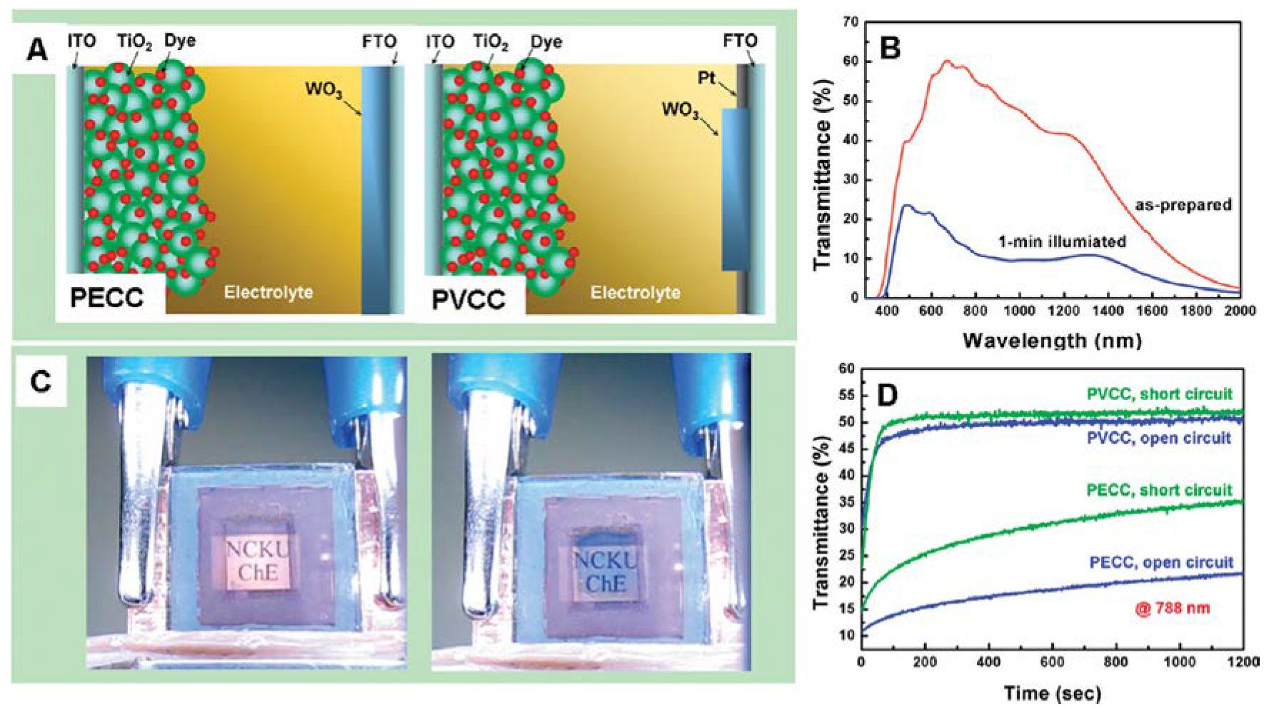
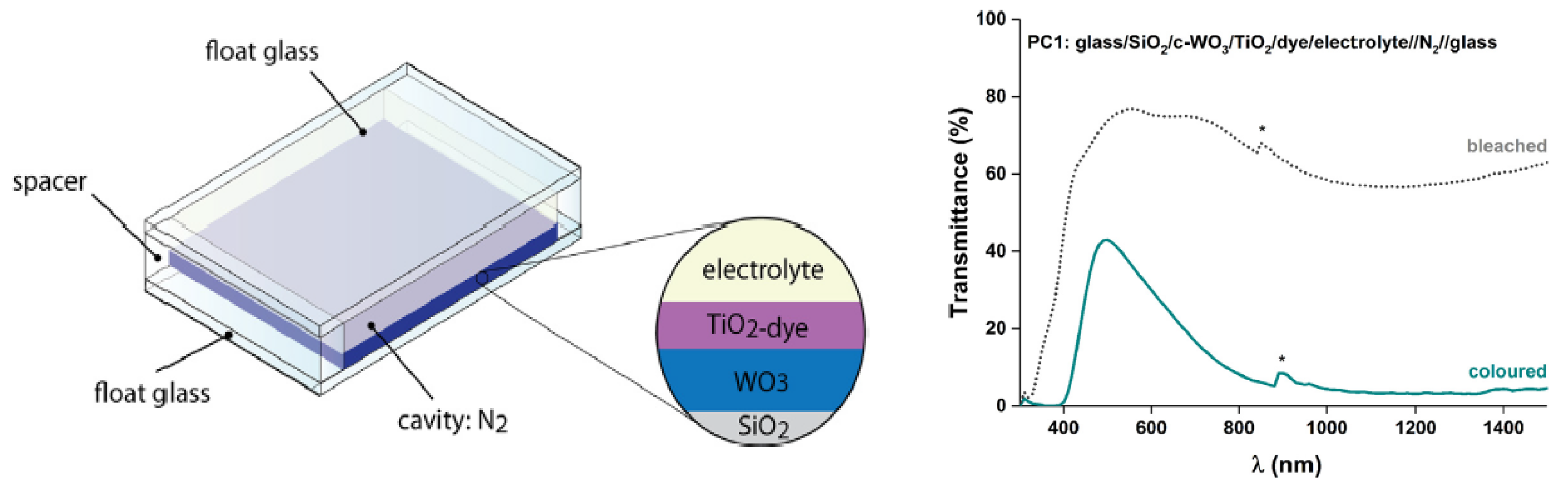
4.2. Photovoltachromic Devices: One Step Forward for PECDs

The first photovoltachromic device (PVCD), (i.e., a PECD that was capable of producing more electric energy than the amount strictly needed to activate smart coloration) was disclosed in 2009 in a paper by Wu et al. [103] (Figure 6). The first PVCDs combined the PV features of dye-sensitized cells and those of PECDs, in a separated architecture. A frame-type layout was adopted, to pattern the WO3/Pt counter electrode. When irradiated, the PVCD underwent very fast coloration (4 s) in short-circuit conditions, whereas bleaching occurred in 40 s. Moreover, a fair PV performance (η = 0.50%) was observed. The very fast kinetics was ascribed to the presence of the Pt catalyst.
A novel design for PVCDs [104] was proposed in 2011, with a special tuning of the electrolyte formulation and a C-shaped Pt frame on the counter electrodes bounding a square region of WO3. In this case, the two areas of the counter electrode were electrically separated, and this allowed for operating the device distinctly as a solar cell or as a PECD, while using two available external circuitries. The smart modulation was accompanied by a relevant increase of efficiency (η = 6.55%). Leftheriotis et al., in 2012 [96], reported a device embodying frame-type opaque (5 μm) TiO2 photoelectrodes instead of highly transparent ones: they measured tcol of about 3 min. and a contrast ratio of 10.2. Yang et al. [105] disclosed a new architecture for a PECD, integrating PProDOT-Me2 as an EC film. The nanofibers of the EC layer were deposited above a thin Pt layer. They achieved tcol of a few seconds and ΔT = 38%. The fibrous structure of the EC material allowed for the contact between the electrolyte and the catalyst layer. The irradiated device cathodically coloured the PProDOT-Me2 film, reached by electrons via external circuitry in short-circuit conditions. After the coloration process was complete, the dye molecules kept on generating electrons, demonstrating encouraging PV output parameters: Open circuit voltage: VOC = 0.66 V; Short-circuit current density jSC = 2.92 mA/cm2; η = 1.12%.
Huang et al. [106] reported a solid-state PV/EC device that embodies thin film solar cells, in the form of stripes; Prussian Blue was used as EC film and LiClO4/PMMA/PC was the electrolyte formulation, touching the full area of the device. They obtained fast modulation of 55% at 690 nm, tcol of 30 s.
A bi-functional counter electrode, with a comb-like pattern of parallel and electrically separated series of stripes was also demonstrated in 2014 [107]. Such stripes were made of WO3 and Pt layers, respectively, allowing for the creation of two distinct circuits that were independently connected to the same highly transparent organic dye-sensitized TiO2 photo-electrode. The stripes on the counter electrode were obtained by high-vacuum deposition techniques and lithographic microfabrication, creating two different pads with interdigitated stripes: the EC stripes were very effective, with very fast coloration (2 s) and bleaching (5 s) time; on the other hand, the Pt stripes enabled fair solar conversion efficiency (η) in the PV circuit. A relevant figure of merit, in this work, was represented by the WO3/Pt area ratio, influencing the η. An orange organic dye enhanced the device transparency and showed relevance for building integration purposes. The thin stripes resulted in being barely visible to the naked eye.
A TiO2 electrode and a transparent cobalt redox couple electrolyte were adopted in a device while using a PProDOT-Et2 film as an EC material [108], achieving a modulation of 34% in 1 s and η of 4.5%. Malara et al. [109] proposed a PVCD in which two overlying counter electrodes were embodied: the intermediate one hosted a thin and transparent Pt layer, acting as a catalyzer, whereas the second one was covered by EC WO3. A crystalline, highly transparent TiO2 and an orange organic dye enhanced the overall transparency of this device. Suitable holes were drilled between the two resulting electrolyte chambers on the central Pt electrode. Consequently, the best PV conversion efficiency η = 2.75% was obtained in devices with the smallest size holes. Distinct operating modes could be easily managed by means of two external circuits. Jensen et al. used a PV electric output [110] to operate a flexible polymer based EC device (employing poly((2,2-bis(2-ethylhexyloxymethyl)-propylene-1,3-dioxy)-3,4-thiophene-2,5-diyl) and poly-(N-octadecyl-(propylene-1,3-dioxy)-3,4-pyrrole-2,5-diyl), reporting a 44% modulation and very fast kinetics (5 s). Dyer et al. [111] coupled PV with EC layers with a fabrication approach foreseeing room temperature solution processing of materials, aiming at roll-to-roll manufacturing. Yang et al. [112] proposed a very stable and durable PVCD embodying a solvent-free hybrid polymer electrolyte (PEG–titanium-based), measuring transmittance modulations of ΔT% of 50% at 788 nm and fast switching times (coloration in 6 s and bleaching in 17 s).
The current trend in devices evokes low-cost and highly effective TCOs that are deposited at room temperature [56] as well as a simplified design philosophy, quickly moving towards single-substrate, solid-state devices. In this roadmap, Hocevar et al. [113] demonstrated a large scale solution processed multi-layered PECDs adopting sol-gel chemistry and dip-coating (Figure 7). Scaled-up devices, with each size of 30 cm, showed a homogeneous contrast of 36% and resulted stable for 12 months. A thin solid electrolyte (25 µm) containing an iodine/iodide redox couple was employed in this device. This device worked as a simplified PECD, almost like a photochromic glass, without any external circuitry to vary its transmittance.
A quasi-solid-state PVCD [114] containing highly transparent perovskite film (with the micro-island morphology exposed in [29]) appeared in 2015. This device used a PEG-plasticized Polyethylene Oxide solid polymer electrolyte. The semi-transparent perovskite-based PV and the EC layer were deposited on as many glass substrates. The top glass had both sides coated to work on both sides, in order to generate electricity on one side and host a transparent ITO film on the other side. The second substrate had WO3 on top. The PEO-PEG-based electrolyte also acted as a “glue”, laminating the two substrates of this device.
This device was designed especially for building integration purpose and it achieved a PV efficiency of 5.5%; a self-modulation of 26% was assessed, being fully activated by the energy output of the PV film, via an external circuitry. Extra-generated power, as soon as the transient coloration process is complete, could be delivered to the grid or used according to the most convenient use. The fabrication process was compatible with lamination, being largely used in the glazing industry.

5. Building Integration of Multifunctional Devices

5.1. Effects on Visual Comfort Durability and Life-Cycle Assessment of Devices

Several studies have hypothesized or demonstrated the effectiveness of smart windows in reducing the energy consumption in buildings or improving comfort level [15,115,116,117]. Such studies showed the relevance of adaptive façade technologies’ support to the challenging issues of containing energy consumption and ecological footprint of buildings. Apart from the mere energy considerations, Piccolo et al. [116] demonstrated that dynamic transition influences indoor visual comfort, showing that a modulation of 54% in sun-oriented windows affects the DGP, achieving sufficient levels of daylighting indoor; at the same time, they also found that windows exposed to West and East require lower values of transmittance for solar radiation incident with lower angles. The manifold effects of PVCDs’ integration in buildings include, of course, improved control of solar radiation [118]. With reference to a standard office room, UDI resulted increased in an average value of 72% and DGP interested 12% of occupied hours.
Tavares et al. [119,120] demonstrated the usefulness of switchable windows in terms of energy savings in air conditioning for sun-oriented (South, West and East) façades.
Zinzi et al. [121] reported an experimental study showing that more than 85% of the occupants did not detect significant variations in the perception of the internal and external space following the chromatic transition of the EC glass. Moreover, only 37% of users did not opt for over-riding the automatic operation of glazing. Subsequently, manual over-ride could be one more feature in the development of chromogenic technologies, mainly compatible with most of the PECDs already appeared in literature.
An adjustable external resistance was in fact proposed by Hauch et al. [89] in order to override the automatic operation of PECDs. To figure out the maximum impact of PVCDs on the energy consumption, Favoino et al. [115] reported a full analysis of an ideal adaptive facade embodying PVCDs, considering their multiple features, finding out that larger optical modulation of SHGC in temperate climates would positively affect the yearly energy balance. Llordes et al. [122] decoupled the transmittance modulation in the visible and NIR range, proposing an effective ‘‘dual-band” technology, showing, by means of ad hoc simulations, that “dual band” EC glazing outperform code-compliant windows (ASHRAE 90-2010) [123]. Lee et al. reported the results of a 20-month study on south-facing large-area EC windows, aiming at the assessment of energy performance, at the NREL Laboratory. They compared the EC devices to a reference window embodying a low-e glazing and a Venetian blind [124]. Lighting energy savings achieved 44–59%. The results showed that the window-lighting control system kept indoor illuminance levels within the ideal setting range for 89–99% of the time.
Another concern for chromogenic façades is represented by durability, since EC windows should overcome 104–106 cycles and reach an overall lifetime of 5–20 years [6,125]. To our knowledge, the latter has not already been demonstrated yet for PECDs, although the issue has been investigated and considered in several studies [91,95,126]. The durability of PECDs is affected by the various technological players influencing their full development, being them complex combination of materials and technologies each one standing at a precise evolution step and causing abrupt steps forward due to sudden breakthroughs (PV and power supply; EC materials’ durability; stability of electrolytes; properties of TCOs; and, etc.). Suitable device designs may, of course, overcome specific limitations and architectural device simplification certainly could affect several figures of merit, including durability. With regards to coloration kinetics, they should be very fast in smart windows, as demonstrated by a specific study [121]. The PECDs appeared in literature so far show fast kinetics, with full coloration in less than 60 s. and, as already observed, the scale-up of devices should not affect the kinetics.
Pierucci et al. [127], in a recent study, assessed the influence of PVCDs on the Life Cycle Impact and Life Cycle Total Energy. They demonstrated that the total impact of PVCDs’ production is lower than that of other technologies that offer similar features. They eventually reported possible reductions of impacts between 41% and 44%, when comparing office buildings equipped, respectively, with PVCDs and commercial solar control glazing, integrated with PV panels to guarantee the same performance.
Moreover, recent research activities in semi-transparent PVs deal with selectively transparent PVs, embodying PV materials that are capable of harvesting UV and NIR wavelengths, without affecting the visible range of transmittance. Subsequently, AVT of 50–90% were achieved [128]. In this new, intriguing research scenario, Davy et al. successfully paired near-UV solar cells with EC conducting polymers, taking advantage of their complementary behavior, from an optical point of view [129]. This example well confirms that, as reviewed elsewhere [32], if a new breakthrough in each component of a PECD steps in, a new technological leap is possible. With reference to the power supply of PECDs, perovskite modules represent the most compatible and promising PV technology from an environmental point of view, as reported by Gong et al. [130], who performed LCA for perovskite solar modules, finding that perovskite solar modules show the shortest energy payback time (EPBT) and the lowest amount of CO2 emission among the eight PV technologies when compared in their study. The EC component itself should take advantage of the development of new EC materials, processed at room temperature, easily scalable, cheap, and with low ecological footprint. This aspect would be crucial towards the exploitation of conductive flexible substrates, especially in the wide field of portable electronics. In this viewpoint, conjugated EC polymers could be used in PECDs, once their main issues, still open, will be overcome (high costs, lower stability, and limited lifetime) [131].
Since the very initial design steps of PECDs, it should be considered that each process should be fully compatible with large-area production in industrial plants employing roll-to-roll, screen printing, or PVD processes; this means that not all of the EC materials or electrolytes investigated so far could be practically (or easily) exploited for the purpose of large-scale production and subsequent spread on the market. As to cost and environmental impact, one should far prefer cheap and abundant materials, rather than rare or toxic ones.
The chance to cut costs and impacts would, of course, be also welcomed by glazing manufacturers and architectural designers. Nowadays, expensive process cost of PECDs may also act as limiting factors for their industrial production and commercial spread. As reported by Casini [132], a wide market spread of smart glazing is slowed down by the high-extra-cost (about 215 €/m2), when compared to code-compliant windows. To promote the spread on the market of smart windows, market analyses suggest that the extra-cost should not be higher than 65 €/m2, by 2025. The development of new materials, especially if solid-state, might offer new knowledge, expanding the benefits deriving from building integration of novel EC technologies.
As recently demonstrated [133], innovative EC devices with a highly compact and simplified device architecture on a single substrate may achieve annual energy saving for air conditioning up to 38%, as compared to a building equipped with clear glass in office buildings. The overall yearly energy saving was instead 25%. Daylighting performance were significantly improved, in terms of both UDI and DGI: sensors reported optimal illuminance conditions in 82.7% of hours, on an annual basis.

5.2. Open Issues, Towards Smart Windows Adopting a Research-Driven Development

The combination of the photoelectrochromic technology with that of semi-transparent PVs would make it possible to avoid the limitation of the rigid optical behavior of shielding systems that are already available on the market, by adapting the visible/solar transmittance profile of glazing to the changing daylighting conditions. In this roadmap, further discussions are required on the possibility (or need) to define appropriate control strategies of the device, as well as to the size of layers and materials, according to location and climate conditions in which the system will operate.
As already stated, the concomitant benefits of PV and PECD glazing may result in relevant energy saving for constructions. For instance, according to a review by Gorgolis et al. [134], building integrated a-Si cells might decrease undesired heat gains by 54.2% and energy consumption for cooling by 28%. PECDs, on the other hand, should fulfil standard requirements for EC glazing, as clearly reported by Lee [135] and Piccolo [136], for example. Some of the parameters that should be fulfilled by PECDs would be, mainly: switching time according to the sky conditions, varying from 5 s to a few minutes; relevant optical memory, from 2 to 24 h; SHGC ranging from 0.6 (bleached conditions) to less than 0.2 in the colored state. Thermal conductivity lower than 1.2 W/m2⋅K; suitable color rendering index, higher than 80; reliability of devices in terms of lifetime (more than 20 years, i.e., more than 25,000 full cycles of coloring an bleaching); operating temperatures compatible with use in buildings (from −30 °C to 90 °C). The effect of these novel technologies on annual energy consumption will be particularly amplified by the fact that, in Europe, as reported by Perez-Lombard et al. [137], energy consumption for HVAC systems reaches 50% of the total.
Table 1, as reported hereafter, shows a synoptic comparison between different chromogenic technologies and semi-transparent PVs for integration in architectural glazing. Additional smart technologies (thermochromic [138,139,140] and photochromic [141,142,143,144] materials) have been added, for a broader and more complete comparison, even if they have not been widely considered in the review. Photochromic and thermochromic materials, when compared to the technologies discussed in this work, in fact, have the undoubted advantage of being able to guarantee the modulation of the spectral properties of the glass, according to an external stimulus (incident solar radiation and temperature, respectively), with simple deposition processes: in fact, the deposition of a single, thin film would be sufficient for obtaining the desired behavior (taking into account several process aspects, like the thickness of the film, concentration of molecules, intrinsic properties of the material used, etc.). The activation of the functionality does not require any energy expenditure as the energy impulse would be provided by the external stimulus itself. On the other hand, these technologies do not allow any form of control by the user or overriding. On the other hand, EC windows allow for a smart modulation of the spectral properties and the user might set the contrast to a favourite, intermediate modulation, or even override the device operation. At the same time, by means of an electronic control system, it is possible to set an optimization strategy, aimed at maximizing energy savings or visual comfort, according to the user’s choice. These devices show a complex architecture, but require very low energy consumption, typically irrelevant, as compared to the yearly energy balance of a building. In fact, as reported by Pal et al. [145], the electrical demand for the EC windows is nearly negligible (1.3 kWh/m2⋅y). Semitransparent PV cells, as compared to chromogenic systems of any type, do not offer the advantage of modulating the contrast in the glazing, due to their fixed optical characteristics. However, it has been observed that, in some climatic conditions, the transmission spectrum of PV glass might be comparable to those of solar control films [80]. In this sense, in particular locations and, in specific façade orientations, semitransparent PV glass can perform multiple functions, in addition to offering electricity production.
The main difference between PECDs and the other chromogenic technologies available today lies in the fact that the energy that is required to activate the chromatic transition is generated in the same device, as a function of the solar radiation incident on its surface. In this sense, modulation is highly responsive, as it is directly modulated by the external stimulus. In this case, in most of the PECDs published in the literature, the user can override the functionality, keeping the device transparent; on the other hand, variable resistance can be applied, in order to limit the modulation, according to specific needs. PVCDs only differ from PECDs in their ability to continuously supply energy to the power grid, after the rapid color transient has occurred.
Especially with reference to PECDs, the open issue of scalability of devices will be relevant, in terms of electrical performance, durability, but also other factors, such as the homogeneity of films and their coloration kinetics. Waiting for the complete scale-up of devices, the preliminary assessment of their large-scale effects plays a relevant role; with this aim, reliable software platform allowing for dynamic simulation can be adopted, while assuming real operating conditions in various locations with different climatic conditions. In fact, building components can be implemented following the “research driven design” approach. The early stage of technology development provides precious experimental data allowing simulations of daylighting penetration and energy use due to building integration of large-scale devices with similar properties. The two levels of activity—experimental and numerical simulations—mutually influence each other. The output of the experimental activity offers interesting inputs for the simulation test, which in turn provides feedbacks for re-design activities, thus considering other parameters (energy consumption or visual comfort), which cannot be considered in the usual laboratory activity devoted to the optimization of materials and devices. Feedbacks of simulations may drive further design and fabrication of devices, even in a cyclic process.

6. Conclusions

Recent scientific trends in the compelling field of energy efficiency of innovative devices clearly show the relevance of newly designed technologies, in order to facilitate the global energy transition, in which our buildings will become more and more energy producers and not just mere consumers. It will be essential, in this scenario, to equip the building envelopes (but above all their window surfaces), with innovative technologies that can not only guarantee energy savings, but also be supplied by or harvest renewable sources. Starting from these considerations, this study investigates two emerging classes of devices that are characterized by a strong level of technological, functional, and performance contiguity: semitransparent PVs and PECDs. This review deals with technologies that are oriented to the design of highly transparent photovoltaic glass, but also of adaptive façades, which are capable of altering their chromatic structure (in the visible and infrared spectrum) as a function of precise variations in solar irradiance. Recent scientific literature, in such fields, shows several points of convergence between the two technological areas mentioned, demonstrating that it is now conceivable a multifunctional glass integrated into the building that is able to perform both the function of PV generation and of solar control, with a welcomed degree of adaptivity. This article presents an accurate, but not exhaustive, review of the devices appeared so far, with particular regard to the evolution of materials technologies, of architectures, performance, reaching the conclusion that the current trend of simplification of solid-state device architectures and reduction of processes’ costs and impacts may eventually help the spread of these energy-saving technologies.

Author Contributions

Conceptualization, A.C.; methodology, A.C.; writing—original draft preparation, A.C.; writing—review and editing, U.A., A.C., F.F., F.M. All authors have read and agreed to the published version of the manuscript.

Funding

This research received no external funding.

Conflicts of Interest

The authors declare no conflict of interest.

References

  1. Nations Unies Convention. Cadre sur les changements climatiques. Proc. Cop. 2015, 21, 39. [Google Scholar]
  2. Armaroli, N.; Balzani, V. Solar Electricity and Solar Fuels: Status and Perspectives in the Context of the Energy Transition. Chem. A Eur. J. 2016, 22, 32–57. [Google Scholar] [CrossRef] [PubMed]
  3. Armaroli, N.; Balzani, V. Towards an electricity-powered world. Energy Environ. Sci. 2011, 4, 3193. [Google Scholar] [CrossRef]
  4. Parliament, E. Directive 2010/31/EU of the European Parlament and of the Council of 19 May 2010 on the Energy Performance of Buildings (recast); The European Parliament: Strasbourg, France; Council of the European Union: Brussels, Belgium, 2010; pp. 13–35. [Google Scholar]
  5. Pichot, F.; Ferrere, S.; Pitts, R.J.; Gregg, B.A. Flexible solid-state photoelectrochromic windows. J. Electrochem. Soc. 1999, 146, 4324–4326. [Google Scholar] [CrossRef]
  6. Lampert, C.M. Optical switching technology for glazings. Thin Solid Films 1993, 236, 6–13. [Google Scholar] [CrossRef]
  7. Reilly, S.; Arasteh, D.; Selkowitz, S. Thermal and optical analysis of switchable window glazings. Sol. Energy Mater. 1991, 22, 1–14. [Google Scholar] [CrossRef] [Green Version]
  8. Zhang, W.; Lu, L.; Peng, J.; Song, A. Comparison of the overall energy performance of semi-transparent photovoltaic windows and common energy-efficient windows in Hong Kong. Energy Build. 2016, 128, 511–518. [Google Scholar] [CrossRef]
  9. Olivieri, L.; Caamaño-Martín, E.; Moralejo-Vázquez, F.J.; Martín-Chivelet, N.; Olivieri, F.; Neila-Gonzalez, F.J. Energy saving potential of semi-transparent photovoltaic elements for building integration. Energy 2014, 76, 572–583. [Google Scholar] [CrossRef] [Green Version]
  10. Benemann, J.; Chehab, O.; Schaar-Gabriel, E. Building-integrated PV modules. Sol. Energy Mater. Sol. Cells 2001, 67, 345–354. [Google Scholar] [CrossRef]
  11. Wang, Y.; Runnerstom, E.L.; Milliron, D.J. Switchable Materials for Smart Windows. Ann. Rev. Chem. Biolmol. Eng. 2016, 7, 1–22. [Google Scholar] [CrossRef]
  12. Rosseinsky, D.R.; Mortimer, R.J. Electrochromic Materials and Devices; Mortimer, R.J., Rosseinsky, D.R., Monk, P.M.S., Eds.; Wiley-VCH Verlag GmbH & Co. KGaA: Weinheim, Germany, 2013; ISBN 9783527679850. [Google Scholar]
  13. Azens, A.; Granqvist, C.G. Electrochromic smart windows: Energy efficiency and device aspects. J. Solid State Electrochem. 2003, 7, 64–68. [Google Scholar] [CrossRef]
  14. Granqvist, C.G. Electrochromics and Thermochromics: Towards a New Paradigm for Energy Efficient Buildings. Mater. Today Proc. 2016, 3, S2–S11. [Google Scholar] [CrossRef]
  15. Granqvist, C.G.; Bayrak Pehlivan, I.; Niklasson, G.A. Electrochromics on a roll: Web-coating and lamination for smart windows. Surf. Coatings Technol. 2017, 336, 6–11. [Google Scholar]
  16. Jonsson, A.; Roos, A. Evaluation of control strategies for different smart window combinations using computer simulations. Sol. Energy 2010, 84, 1–9. [Google Scholar] [CrossRef]
  17. Gugliermetti, F.; Bisegna, F. Visual and energy management of electrochromic windows in Mediterranean climate. Build. Environ. 2003, 38, 479–492. [Google Scholar] [CrossRef]
  18. Piccolo, A.; Simone, F. Energy performance of an all solid state electrochromic prototype for smart window applications. Energy Procedia 2015, 78, 110–115. [Google Scholar] [CrossRef] [Green Version]
  19. Bechinger, C.; Ferrere, S.; Zaban, A.; Sprague, J.; Gregg, B.A. Photoelectrochromic windows and displays. Nature 1996, 383, 608–610. [Google Scholar] [CrossRef]
  20. Deb, S.K.; Lee, S.H.; Edwin Tracy, C.; Roland Pitts, J.; Gregg, B.A.; Branz, H.M. Stand-alone photovoltaic-powered electrochromic smart window. Electrochim. Acta 2001, 46, 2125–2130. [Google Scholar] [CrossRef]
  21. Gregg, B.A. Photoelectrochromic applications. Endeavour 1997, 21, 52–55. [Google Scholar] [CrossRef]
  22. Heinstein, P.; Ballif, C.; Perret-Aebi, L.E. Building integrated photovoltaics (BIPV): Review, potentials, barriers and myths. Green 2013, 3, 125–156. [Google Scholar] [CrossRef]
  23. Sprenger, W.; Wilson, H.R.; Kuhn, T.E. Electricity yield simulation for the building-integrated photovoltaic system installed in the main building roof of the Fraunhofer Institute for Solar Energy Systems ISE. Sol. Energy 2016, 135, 633–643. [Google Scholar] [CrossRef]
  24. Jelle, B.P.; Breivik, C.; Drolsum Røkenes, H. Building integrated photovoltaic products: A state-of-the-art review and future research opportunities. Sol. Energy Mater. Sol. Cells 2012, 100, 69–96. [Google Scholar] [CrossRef] [Green Version]
  25. Oliver, M.; Jackson, T. Energy and economic evaluation of building-integrated photovoltaics. Energy 2001, 26, 431–439. [Google Scholar] [CrossRef]
  26. Jelle, B.P.; Breivik, C. The path to the building integrated photovoltaics of tomorrow. Energy Procedia 2012, 20, 78–87. [Google Scholar] [CrossRef] [Green Version]
  27. Saifullah, M.; Gwak, J.; Yun, J.H. Comprehensive review on material requirements, present status, and future prospects for building-integrated semitransparent photovoltaics (BISTPV). J. Mater. Chem. A 2016, 4, 8512–8540. [Google Scholar] [CrossRef]
  28. Jelle, B.P. Electrochromic Smart Windows for Dynamic Daylight and Solar Energy Control in Buildings. In Electrochromic Materials and Devices; Monk, P.M.S., Mortimer, R.J., Rosseinsky, D.R., Eds.; Wiley: Hoboken, NJ, USA, 2015; pp. 419–502. [Google Scholar]
  29. Eperon, G.E.; Burlakov, V.M.; Goriely, A.; Snaith, H.J. Neutral color semitransparent microstructured perovskite solar cells. ACS Nano 2014, 8, 591–598. [Google Scholar] [CrossRef]
  30. Boyce, P.; Eklund, N.; Mangum, S.; Saalfield, C.; Tang, L. Minimum acceptable transmittance of glazing. Light. Res. Technol. 1995, 27, 145–152. [Google Scholar] [CrossRef]
  31. Baetens, R.; Jelle, B.P.; Gustavsen, A. Properties, requirements and possibilities of smart windows for dynamic daylight and solar energy control in buildings: A state-of-the-art review. Sol. Energy Mater. Sol. Cells 2010, 94, 87–105. [Google Scholar] [CrossRef] [Green Version]
  32. Cannavale, A.; Cossari, P.; Eperon, G.E.; Colella, S.; Fiorito, F.; Gigli, G.; Snaith, H.J.; Listorti, A. Forthcoming perspectives of photoelectrochromic devices: A critical review. Energy Environ. Sci. 2016, 9, 2682–2719. [Google Scholar] [CrossRef]
  33. Hagfeldt, A.; Boschloo, G.; Sun, L.; Kloo, L.; Pettersson, H.; Kalyanasundaram, E.K.; Bertoz, M.; Bisquert, J.; De Angelis, F.; Desilvestro, H.; et al. Dye-sensitized solar cells. Chem. Rev. 2010, 110, 6595–6663. [Google Scholar] [CrossRef]
  34. Manca, M.; Beke, S.; De Marco, L.; Pareo, P.; Qualtieri, A.; Cannavale, A.; Brandi, F.; Gigli, G. 3D photoelectrode for dye solar cells realized by laser micromachining of photosensitive glass. J. Phys. Chem. C 2014, 118, 17100–17107. [Google Scholar] [CrossRef] [Green Version]
  35. Carlson, D.E.; Wronski, C.R. Amorphous silicon solar cell. Appl. Phys. Lett. 1976, 28, 671–673. [Google Scholar] [CrossRef]
  36. Yalçin, L.; Öztürk, R. Performance comparison of c-Si, mc-Si and a-Si thin film PV by PVsyst simulation. J. Optoelectron. Adv. Mater. 2013, 15, 326–334. [Google Scholar]
  37. Song, Y.; Chang, S.; Gradecak, S.; Kong, J. Visibly-Transparent Organic Solar Cells on Flexible Substrates with All-Graphene Electrodes. Adv. Energy Mater. 2016, 6, 1600847. [Google Scholar] [CrossRef]
  38. Della Gaspera, E.; Peng, Y.; Hou, Q.; Spiccia, L.; Bach, U.; Jasieniak, J.J.; Cheng, Y.B. Ultra-thin high efficiency semitransparent perovskite solar cells. Nano Energy 2015, 13, 249–257. [Google Scholar] [CrossRef]
  39. Kim, T.; Kim, J.H.; Kang, T.E.; Lee, C.; Kang, H.; Shin, M.; Wang, C.; Ma, B.; Jeong, U.; Kim, T.S.; et al. Flexible, highly efficient all-polymer solar cells. Nat. Commun. 2015, 6, 1–7. [Google Scholar] [CrossRef] [Green Version]
  40. O’Regan, B.; Gratzel, M. A Low-Cost, High-Efficiency Solar-Cell Based on Dye-Sensitized Colloidal TiO2 Films. Nature 1991, 353, 737–740. [Google Scholar] [CrossRef]
  41. Gong, J.; Sumathy, K.; Qiao, Q.; Zhou, Z. Review on dye-sensitized solar cells (DSSCs): Advanced techniques and research trends. Renew. Sustain. Energy Rev. 2017, 68, 234–246. [Google Scholar] [CrossRef]
  42. Lee, C.; Li, C.; Ho, K. Use of organic materials in dye-sensitized solar cells. Biochem. Pharmacol. 2017, 20, 267–283. [Google Scholar] [CrossRef]
  43. Parisi, M.L.; Maranghi, S.; Basosi, R. The evolution of the dye sensitized solar cells from Grätzel prototype to up-scaled solar applications: A life cycle assessment approach. Renew. Sustain. Energy Rev. 2014, 39, 124–138. [Google Scholar] [CrossRef]
  44. Selvaraj, P.; Ghosh, A.; Mallick, T.K.; Sundaram, S. Investigation of semi-transparent dye-sensitized solar cells for fenestration integration. Renew. Energy 2019, 141, 516–525. [Google Scholar] [CrossRef]
  45. Fakharuddin, A.; Jose, R.; Brown, T.M.; Fabregat-Santiago, F.; Bisquert, J. A perspective on the production of dye-sensitized solar modules. Energy Environ. Sci. 2014, 7, 3952–3981. [Google Scholar] [CrossRef]
  46. Kitamura, T.; Okada, K.; Matsui, H.; Tanabe, N. Durability of Dye-Sensitized Solar Cells and Modules. J. Sol. Energy Eng. 2016, 132, 1–7. [Google Scholar] [CrossRef]
  47. Reale, A.; Cinà, L.; Malatesta, A.; De Marco, R.; Brown, T.M.; Di Carlo, A. Estimation of Energy Production of Dye-Sensitized Solar Cell Modules for Building-Integrated Photovoltaic Applications. Energy Technol. 2014, 2, 531–541. [Google Scholar] [CrossRef]
  48. El Chaar, L.; Lamont, L.A.; El Zein, N. Review of photovoltaic technologies. Renew. Sustain. Energy Rev. 2011, 15, 2165–2175. [Google Scholar] [CrossRef]
  49. Fritzsche, H. Photo-induced structural changes associated with the Staebler-Wronski effect in hydrogenated amorphous silicon. Solid State Commun. 1995, 94, 953–955. [Google Scholar] [CrossRef]
  50. Águas, H.; Ram, S.K.; Araújo, A.; Gaspar, D.; Vicente, A.; Filonovich, S.A.; Fortunato, E.; Martins, R.; Ferreira, I. Silicon thin film solar cells on commercial tiles. Energy Environ. Sci. 2011, 4, 4620. [Google Scholar] [CrossRef]
  51. Narain, J.; Jin, W.; Ghandehari, M.; Wilke, E.; Shukla, N.; Berardi, U.; El-Korchi, T.; Van Dessel, S. Design and Application of Concrete Tiles Enhanced with Microencapsulated Phase-Change Material. J. Archit. Eng. 2016, 22, 05015003. [Google Scholar] [CrossRef]
  52. Chae, Y.T.; Kim, J.; Park, H.; Shin, B. Building energy performance evaluation of building integrated photovoltaic (BIPV) window with semi-transparent solar cells. Appl. Energy 2014, 129, 217–227. [Google Scholar] [CrossRef]
  53. Krebs, F.C.; Espinosa, N.; Hösel, M.; Søndergaard, R.R.; Jørgensen, M. 25th anniversary article: Rise to power-OPV-based solar parks. Adv. Mater. 2014, 26, 29–39. [Google Scholar] [CrossRef]
  54. Chen, C.C.; Dou, L.; Zhu, R.; Chung, C.H.; Song, T.B.; Zheng, Y.B.; Hawks, S.; Li, G.; Weiss, P.S.; Yang, Y. Visibly transparent polymer solar cells produced by solution processing. ACS Nano 2012, 6, 7185–7190. [Google Scholar] [CrossRef] [PubMed]
  55. Van Der Wiel, B.; Egelhaaf, H.J.; Issa, H.; Roos, M.; Henze, N. Market readiness of organic photovoltaics for building integration. Twent. Century Music 2014, 1639. [Google Scholar] [CrossRef]
  56. Granqvist, C.G. Transparent conductors as solar energy materials: A panoramic review. Sol. Energy Mater. Sol. Cells 2007, 91, 1529–1598. [Google Scholar] [CrossRef]
  57. Zhang, S.; Lanty, G.; Lauret, J.S.; Deleporte, E.; Audebert, P.; Galmiche, L. Synthesis and optical properties of novel organic-inorganic hybrid nanolayer structure semiconductors. Acta Mater. 2009, 57, 3301–3309. [Google Scholar] [CrossRef]
  58. Green, M.; Ho-baillie, A. The emergence of perovskite solar cells. Nat. Photonics 2014, 8, 506–514. [Google Scholar] [CrossRef]
  59. Kim, H.S.; Lee, C.R.; Im, J.H.; Lee, K.B.; Moehl, T.; Marchioro, A.; Moon, S.J.; Humphry-Baker, R.; Yum, J.H.; Moser, J.E.; et al. Lead iodide perovskite sensitized all-solid-state submicron thin film mesoscopic solar cell with efficiency exceeding 9%. Sci. Rep. 2012, 2, 1–7. [Google Scholar] [CrossRef] [PubMed] [Green Version]
  60. Chang, N.L.; Yi Ho-Baillie, A.W.; Basore, P.A.; Young, T.L.; Evans, R.; Egan, R.J. A manufacturing cost estimation method with uncertainty analysis and its application to perovskite on glass photovoltaic modules. Prog. Photovolt. Res. Appl. 2017, 25, 390–405. [Google Scholar] [CrossRef]
  61. Qin, P.; Tanaka, S.; Ito, S.; Tetreault, N.; Manabe, K.; Nishino, H.; Nazeeruddin, M.K.; Grätzel, M. Inorganic hole conductor-based lead halide perovskite solar cells with 12.4% conversion efficiency. Nat. Commun. 2014, 5, 1–6. [Google Scholar] [CrossRef] [Green Version]
  62. Eperon, G.E.; Leijtens, T.; Bush, K.A.; Prasanna, R.; Green, T.; Wang, J.T.; Mcmeekin, D.P.; Volonakis, G.; Milot, R.L.; May, R.; et al. Perovskite-perovskite tandem photovoltaics with optimized bandgaps. Science 2016, 9717, 1–10. [Google Scholar]
  63. NREL Best Research-Cell Efficiency Chart. Available online: https://www.nrel.gov/pv/cell-efficiency.html (accessed on 19 November 2019).
  64. Park, N.G. Research Direction toward Scalable, Stable, and High Efficiency Perovskite Solar Cells. Adv. Energy Mater. 2019, 1903106, 1–14. [Google Scholar] [CrossRef]
  65. Noel, N.K.; Stranks, S.D.; Abate, A.; Wehrenfennig, C.; Guarnera, S.; Haghighirad, A.-A.; Sadhanala, A.; Eperon, G.E.; Pathak, S.K.; Johnston, M.B.; et al. Lead-free organic–inorganic tin halide perovskites for photovoltaic applications. Energy Environ. Sci. 2014, 7, 3061–3068. [Google Scholar] [CrossRef]
  66. Christians, J.A.; Schulz, P.; Tinkham, J.S.; Schloemer, T.H.; Harvey, S.P.; Tremolet De Villers, B.J.; Sellinger, A.; Berry, J.J.; Luther, J.M. Tailored interfaces of unencapsulated perovskite solar cells for 1000 hour operational stability. Nat. Energy 2018, 3, 68–74. [Google Scholar] [CrossRef]
  67. Park, N.-G.; Grätzel, M.; Miyasaka, T.; Zhu, K.; Emery, K. Towards stable and commercially available perovskite solar cells. Nat. Energy 2016, 1, 16152. [Google Scholar] [CrossRef]
  68. Song, Z.; McElvany, C.L.; Phillips, A.B.; Celik, I.; Krantz, P.W.; Watthage, S.C.; Liyanage, G.K.; Apul, D.; Heben, M.J. A technoeconomic analysis of perovskite solar module manufacturing with low-cost materials and techniques. Energy Environ. Sci. 2017, 10, 1297–1305. [Google Scholar] [CrossRef]
  69. Eperon, G.E.; Stranks, S.D.; Menelaou, C.; Johnston, M.B.; Herz, L.M.; Snaith, H.J. Formamidinium lead trihalide: A broadly tunable perovskite for efficient planar heterojunction solar cells. Energy Environ. Sci. 2014, 7, 982. [Google Scholar] [CrossRef]
  70. Zhang, W.; Anaya, M.; Lozano, G.; Calvo, M.E.; Johnston, M.B.; Míguez, H.; Snaith, H.J. Highly efficient perovskite solar cells with tunable structural color. Nano Lett. 2015, 15, 1698–1702. [Google Scholar] [CrossRef] [Green Version]
  71. Hörantner, M.T.; Nayak, P.K.; Mukhopadhyay, S.; Wojciechowski, K.; Beck, C.; McMeekin, D.; Kamino, B.; Eperon, G.E.; Snaith, H.J. Shunt-Blocking Layers for Semitransparent Perovskite Solar Cells. Adv. Mater. Interfaces 2016, 3, 1–7. [Google Scholar] [CrossRef]
  72. Aharon, S.; Layani, M.; Cohen, B.E.; Shukrun, E.; Magdassi, S.; Etgar, L. Self-Assembly of Perovskite for Fabrication of Semitransparent Perovskite Solar Cells. Adv. Mater. Interfaces 2015, 2, 1–6. [Google Scholar] [CrossRef]
  73. Ramírez Quiroz, C.O.; Levchuk, I.; Bronnbauer, C.; Salvador, M.; Forberich, K.; Heumüller, T.; Hou, Y.; Schweizer, P.; Spiecker, E.; Brabec, C.J. Pushing efficiency limits for semitransparent perovskite solar cells. J. Mater. Chem. A 2015, 3, 24071–24081. [Google Scholar] [CrossRef] [Green Version]
  74. Yang, R.J.; Zou, P.X.W. Building integrated photovoltaics (BIPV): Costs, benefits, risks, barriers and improvement strategy. Int. J. Constr. Manag. 2016, 16, 39–53. [Google Scholar] [CrossRef]
  75. Eke, R.; Senturk, A. Monitoring the performance of single and triple junction amorphous silicon modules in two building integrated photovoltaic (BIPV) installations. Appl. Energy 2013, 109, 154–162. [Google Scholar] [CrossRef]
  76. Kapsis, K.; Athienitis, A.K. A study of the potential benefits of semi-transparent photovoltaics in commercial buildings. Sol. Energy 2015, 115, 120–132. [Google Scholar] [CrossRef]
  77. Zomer, C.; Nobre, A.; Cassatella, P.; Reindl, T.; Rüther, R. The balance between aesthetics and performance in building-integrated photovoltaics in the tropics. Prog. Photovoltaics Res. Appl. 2013, 22, 744–756. [Google Scholar] [CrossRef]
  78. Lim, J.W.; Lee, S.H.; Lee, D.J.; Lee, Y.J.; Yun, S.J. Performances of amorphous silicon and silicon germanium semi-transparent solar cells. Thin Solid Films 2013, 547, 212–215. [Google Scholar] [CrossRef]
  79. Martellotta, F.; Cannavale, A.; Ayr, U. Comparing energy performance of different semi-transparent, building-integrated photovoltaic cells applied to “reference” buildings. Energy Procedia 2017, 126, 219–226. [Google Scholar] [CrossRef]
  80. Cannavale, A.; Hörantner, M.; Eperon, G.E.; Snaith, H.J.; Fiorito, F.; Ayr, U.; Martellotta, F. Building integration of semitransparent perovskite-based solar cells: Energy performance and visual comfort assessment. Appl. Energy 2017, 194, 94–107. [Google Scholar] [CrossRef]
  81. Nabil, A.; Mardaljevic, J. Useful daylight illuminances: A replacement for daylight factors. Energy Build. 2006, 38, 905–913. [Google Scholar] [CrossRef]
  82. Nabil, A.; Mardaljevic, J. Useful daylight illuminance: A new paradigm for assessing daylight in buildings. Light. Res. Technol. 2005, 37, 41–59. [Google Scholar] [CrossRef]
  83. Wienold, J.; Christoffersen, J. Evaluation methods and development of a new glare prediction model for daylight environments with the use of CCD cameras. Energy Build. 2006, 38, 743–757. [Google Scholar] [CrossRef]
  84. Cannavale, A.; Ayr, U.; Martellotta, F. Energetic and visual comfort implications of using perovskite-based building-integrated photovoltaic glazings. Energy Procedia 2017, 126, 636–643. [Google Scholar] [CrossRef]
  85. Cannavale, A.; Ierardi, L.; Hörantner, M.; Eperon, G.E.; Snaith, H.J.; Ayr, U.; Martellotta, F. Improving energy and visual performance in offices using building integrated perovskite-based solar cells: A case study in Southern Italy. Appl. Energy 2017, 205, 834–836. [Google Scholar] [CrossRef]
  86. Jelle, B.P. Building integrated photovoltaics: A concise description of the current state of the art and possible research pathways. Energies 2016, 9, 21. [Google Scholar] [CrossRef] [Green Version]
  87. Attoye, D.E.; Aoul, K.A.T.; Hassan, A. A review on building integrated photovoltaic façade customization potentials. Sustainability 2017, 9, 2287. [Google Scholar] [CrossRef] [Green Version]
  88. Li, Y.; Hagen, J.; Haarer, D. Novel photoelectrochromic cells containing a polyaniline layer and a dye-sensitized nanocrystalline TiO2 photovoltaic cell. Synth. Met. 1998, 94, 273–277. [Google Scholar] [CrossRef]
  89. Hauch, A.; Georg, A.; Baumgärtner, S.; Opara Krašovec, U.; Orel, B. New photoelectrochromic device. Electrochim. Acta 2001, 46, 2131–2136. [Google Scholar] [CrossRef]
  90. Liao, J.Y.; Ho, K.C. A photoelectrochromic device using a PEDOT thin film. J. New Mater. Electrochem. Syst. 2005, 8, 37–47. [Google Scholar]
  91. Krašovec, U.O.; Georg, A.; Georg, A.; Wittwer, V.; Luther, J.; Topič, M. Performance of a solid-state photoelectrochromic device. Sol. Energy Mater. Sol. Cells 2004, 84, 369–380. [Google Scholar] [CrossRef]
  92. Georg, A.; Georg, A.; Opara Krašovec, U. Photoelectrochromic window with Pt catalyst. Thin Solid Films 2006, 502, 246–251. [Google Scholar] [CrossRef]
  93. Santa-Nokki, H.; Kallioinen, J.; Korppi-Tommola, J. A dye-sensitized solar cell driven electrochromic device. Photochem. Photobiol. Sci. 2007, 6, 63–66. [Google Scholar] [CrossRef] [PubMed]
  94. Hsu, C.Y.; Lee, K.M.; Huang, J.H.; Justin Thomas, K.R.; Lin, J.T.; Ho, K.C. A novel photoelectrochromic device with dual application based on poly(3,4-alkylenedioxythiophene) thin film and an organic dye. J. Power Sources 2008, 185, 1505–1508. [Google Scholar] [CrossRef]
  95. Leftheriotis, G.; Syrrokostas, G.; Yianoulis, P. Development of photoelectrochromic devices for dynamic solar control in buildings. Sol. Energy Mater. Sol. Cells 2010, 94, 2304–2313. [Google Scholar] [CrossRef]
  96. Leftheriotis, G.; Syrrokostas, G.; Yianoulis, P. Partly covered photoelectrochromic devices with enhanced coloration speed and efficiency. Sol. Energy Mater. Sol. Cells 2012, 96, 86–92. [Google Scholar] [CrossRef]
  97. Dokouzis, A.; Theodosiou, K.; Leftheriotis, G. Assessment of the long-term performance of partly covered photoelectrochromic devices under insolation and in storage. Sol. Energy Mater. Sol. Cells 2018, 182, 281–293. [Google Scholar] [CrossRef]
  98. Theodosiou, Κ.; Dokouzis, A.; Antoniou, I.; Leftheriotis, G. Gel electrolytes for partly covered photoelectrochromic devices. Sol. Energy Mater. Sol. Cells 2019, 202, 110124. [Google Scholar] [CrossRef]
  99. Lin, C.-L.; Chen, C.-Y.; Yu, H.-F.; Ho, K.-C. Comparisons of the electrochromic properties of Poly(hydroxymethyl 3,4-ethylenedioxythiophene) and Poly(3,4- ethylenedioxythiophene) thin films and the photoelectrochromic devices using these thin films. Sol. Energy Mater. Sol. Cells 2019, 202, 110132. [Google Scholar] [CrossRef]
  100. Dokouzis, A.; Bella, F.; Theodosiou, K.; Gerbaldi, C.; Leftheriotis, G. Photoelectrochromic devices with cobalt redox electrolytes. Mater. Today Energy 2020, 15, 100365. [Google Scholar] [CrossRef]
  101. Shen, K.; Luo, G.; Liu, J.; Zheng, J.; Xu, C. Highly transparent photoelectrochromic device based on carbon quantum dots sensitized photoanode. Sol. Energy Mater. Sol. Cells 2019, 193, 372–378. [Google Scholar] [CrossRef]
  102. Guo, X.; Xu, Z.; Huang, J.; Zhang, Y.; Liu, X.; Guo, W. Photoelectrochromic smart windows powered by flexible dye-sensitized solar cell using CuS mesh as counter electrode. Mater. Lett. 2019, 244, 92–95. [Google Scholar] [CrossRef]
  103. Wu, J.J.; Hsieh, M.D.; Liao, W.P.; Wu, W.T.; Chen, J.S. Fast-switching photovoltachromic cells with tunable transmittance. ACS Nano 2009, 3, 2297–2303. [Google Scholar] [CrossRef]
  104. Cannavale, A.; Manca, M.; Malara, F.; De Marco, L.; Cingolani, R.; Gigli, G. Highly efficient smart photovoltachromic devices with tailored electrolyte composition. Energy Environ. Sci. 2011, 4, 2567–2574. [Google Scholar] [CrossRef]
  105. Yang, S.; Zheng, J.; Li, M.; Xu, C. A novel photoelectrochromic device based on poly(3,4-(2,2- dimethylpropylenedioxy)thiophene) thin film and dye-sensitized solar cell. Sol. Energy Mater. Sol. Cells 2012, 97, 186–190. [Google Scholar] [CrossRef]
  106. Huang, L.M.; Kung, C.P.; Hu, C.W.; Peng, C.Y.; Liu, H.C. Tunable photovoltaic electrochromic device and module. Sol. Energy Mater. Sol. Cells 2012, 107, 390–395. [Google Scholar] [CrossRef]
  107. Cannavale, A.; Manca, M.; De Marco, L.; Grisorio, R.; Carallo, S.; Suranna, G.P.; Gigli, G. Photovoltachromic device with a micropatterned bifunctional counter electrode. ACS Appl. Mater. Interfaces 2014, 6, 2415–2422. [Google Scholar] [CrossRef] [PubMed]
  108. Amasawa, E.; Sasagawa, N.; Kimura, M.; Taya, M. Design of a new energy-harvesting electrochromic window based on an organic polymeric dye, a cobalt couple, and PProDOT-Me2. Adv. Energy Mater. 2014, 4, 1–9. [Google Scholar] [CrossRef]
  109. Malara, F.; Cannavale, A.; Carallo, S.; Gigli, G. Smart windows for building integration: A new architecture for photovoltachromic devices. ACS Appl. Mater. Interfaces 2014, 6, 9290–9297. [Google Scholar] [CrossRef]
  110. Jensen, J.; Dam, H.F.; Reynolds, J.R.; Dyer, A.L.; Krebs, F.C. Manufacture and demonstration of organic photovoltaic-powered electrochromic displays using roll coating methods and printable electrolytes. J. Polym. Sci. Part B Polym. Phys. 2012, 50, 536–545. [Google Scholar] [CrossRef]
  111. Dyer, A.L.; Bulloch, R.H.; Zhou, Y.; Kippelen, B.; Reynolds, J.R.; Zhang, F. A vertically integrated solar-powered electrochromic window for energy efficient buildings. Adv. Mater. 2014, 26, 4895–4900. [Google Scholar] [CrossRef]
  112. Yang, M.-C.; Cho, H.-W.; Wu, J.-J. Fabrication of stable photovoltachromic cells using a solvent-free hybrid polymer electrolyte. Nanoscale 2014, 6, 9541–9544. [Google Scholar] [CrossRef]
  113. Hočevar, M.; Opara Krašovec, U. A photochromic single glass pane. Sol. Energy Mater. Sol. Cells 2018, 186, 111–114. [Google Scholar] [CrossRef]
  114. Cannavale, A.; Eperon, G.E.; Cossari, P.; Abate, A.; Snaith, H.J.; Gigli, G. Perovskite photovoltachromic cells for building integration. Energy Environ. Sci. 2015, 8, 1578–1584. [Google Scholar] [CrossRef]
  115. Favoino, F.; Fiorito, F.; Cannavale, A.; Ranzi, G.; Overend, M. Optimal control and performance of photovoltachromic switchable glazing for building integration in temperate climates. Appl. Energy 2016, 178, 943–961. [Google Scholar] [CrossRef] [Green Version]
  116. Piccolo, A.; Simone, F. Effect of switchable glazing on discomfort glare from windows. Build. Environ. 2009, 44, 1171–1180. [Google Scholar] [CrossRef]
  117. Xie, Z.; Jin, X.; Chen, G.; Xu, J.; Chen, D.; Shen, G. Integrated smart electrochromic windows for energy saving and storage applications. Chem. Commun. 2014, 50, 608–610. [Google Scholar] [CrossRef] [PubMed]
  118. Cannavale, A.; Fiorito, F.; Resta, D.; Gigli, G. Visual comfort assessment of smart photovoltachromic windows. Energy Build. 2013, 65, 137–145. [Google Scholar] [CrossRef]
  119. Tavares, P.F.; Gaspar, A.R.; Martins, A.G.; Frontini, F. Evaluation of electrochromic windows impact in the energy performance of buildings in mediterranean climates. Energy Policy 2014, 67, 68–81. [Google Scholar] [CrossRef] [Green Version]
  120. Tavares, P.; Bernardo, H.; Gaspar, A.; Martins, A. Control criteria of electrochromic glasses for energy savings in mediterranean buildings refurbishment. Sol. Energy 2016, 134, 236–250. [Google Scholar] [CrossRef] [Green Version]
  121. Zinzi, M. Office worker preferences of electrochromic windows: A pilot study. Build. Environ. 2006, 41, 1262–1273. [Google Scholar] [CrossRef]
  122. Llordés, A.; Garcia, G.; Gazquez, J.; Milliron, D.J. Tunable near-infrared and visible-light transmittance in nanocrystal-in-glass composites. Nature 2013, 500, 323–326. [Google Scholar] [CrossRef]
  123. DeForest, N.; Shehabi, A.; Selkowitz, S.; Milliron, D.J. A comparative energy analysis of three electrochromic glazing technologies in commercial and residential buildings. Appl. Energy 2017, 192, 95–109. [Google Scholar] [CrossRef] [Green Version]
  124. Lee, E.S.; Dibartolomeo, D.L.; Selkowitz, S.E. Daylighting control performance of a thin-film ceramic electrochromic window: Field study results. Energy Build. 2006, 38, 30–44. [Google Scholar] [CrossRef]
  125. Lampert, C.M. Chromogenic smart materials. Mater. Today 2004, 7, 28–35. [Google Scholar] [CrossRef]
  126. Leftheriotis, G.; Syrrokostas, G.; Yianoulis, P. Photocoloration efficiency and stability of photoelectrochromic devices. Solid State Ionics 2013, 231, 30–36. [Google Scholar] [CrossRef]
  127. Pierucci, A.; Cannavale, A.; Martellotta, F.; Fiorito, F. Smart windows for carbon neutral buildings. A Life Cycle approach. Energy Build. 2018, 165, 160–171. [Google Scholar] [CrossRef]
  128. Traverse, C.J.; Pandey, R.; Barr, M.C.; Lunt, R.R. Emergence of highly transparent photovoltaics for distributed applications. Nat. Energy 2017, 2, 849–860. [Google Scholar] [CrossRef]
  129. Davy, N.C.; Sezen-edmonds, M.; Gao, J.; Lin, X.; Liu, A.; Yao, N.; Kahn, A. Pairing of near-ultraviolet solar cells with electrochromic windows for smart management of the solar spectrum. Nat. Energy 2017, 17104, 1–10. [Google Scholar]
  130. Gong, J.; Darling, S.B.; You, F. Perovskite photovoltaics: Life-cycle assessment of energy and environmental impacts. Energy Environ. Sci. 2015, 8, 1953–1968. [Google Scholar] [CrossRef]
  131. Ho, K.C.; Chen, H.W.; Hsu, C.Y. Photoelectrochromic Materials and Devices. Electrochromic Mater. Devices 2015, 593–622. [Google Scholar]
  132. Casini, M. Sustainable Solutions for Energy Efficiency of Buildings. In Proceedings of the 15th International Multidisciplinary Scientific GeoConference & EXPO SGEM 2015, Albena, Bulgaria, 16–25 June 2015; Volume 2, pp. 303–310. [Google Scholar]
  133. Cannavale, A.; Martellotta, F.; Cossari, P.; Gigli, G. Energy savings due to building integration of innovative solid-state electrochromic devices. Appl. Energy 2018, 225, 975–985. [Google Scholar] [CrossRef]
  134. Gorgolis, G.; Karamanis, D. Solar energy materials for glazing technologies. Sol. Energy Mater. Sol. Cells 2016, 144, 559–578. [Google Scholar] [CrossRef]
  135. Lee, E. Application issues for large-area electrochromic windows in commercial buildings. Sol. Energy Mater. Sol. Cells 2002, 71, 465–491. [Google Scholar] [CrossRef] [Green Version]
  136. Piccolo, A.; Simone, F. Performance requirements for electrochromic smart window. J. Build. Eng. 2015, 3, 94–103. [Google Scholar] [CrossRef]
  137. Pérez-Lombard, L.; Ortiz, J.; Pout, C. A review on buildings energy consumption information. Energy Build. 2008, 40, 394–398. [Google Scholar] [CrossRef]
  138. Granqvist, C.G.; Lansåker, P.C.; Mlyuka, N.R.; Niklasson, G.A.; Avendaño, E. Progress in chromogenics: New results for electrochromic and thermochromic materials and devices. Sol. Energy Mater. Sol. Cells 2009, 93, 2032–2039. [Google Scholar] [CrossRef]
  139. Tällberg, R.; Jelle, B.P.; Loonen, R.; Gao, T.; Hamdy, M. Comparison of the energy saving potential of adaptive and controllable smart windows: A state-of-the-art review and simulation studies of thermochromic, photochromic and electrochromic technologies. Sol. Energy Mater. Sol. Cells 2019, 200, 109828. [Google Scholar] [CrossRef] [Green Version]
  140. Costanzo, V.; Evola, G.; Marletta, L. Thermal and visual performance of real and theoretical thermochromic glazing solutions for office buildings. Sol. Energy Mater. Sol. Cells 2016, 149, 110–120. [Google Scholar] [CrossRef]
  141. Cipolloni, M.; Heynderickx, A.; Maurel, F.; Perrier, A.; Jacquemin, D.; Siri, O.; Ortica, F.; Favaro, G. Multiswitchable acidichromic and photochromic bisdiarylethene. An experimental and theoretical study. J. Phys. Chem. C 2011, 115, 23096–23106. [Google Scholar] [CrossRef]
  142. Zhang, J.; Zou, Q.; Tian, H. Photochromic materials: More than meets the eye. Adv. Mater. 2013, 25, 378–399. [Google Scholar] [CrossRef] [PubMed]
  143. Ke, Y.; Chen, J.; Lin, G.; Wang, S.; Zhou, Y.; Yin, J.; Lee, P.S.; Long, Y. Smart Windows: Electro-, Thermo-, Mechano-, Photochromics, and Beyond. Adv. Energy Mater. 2019, 9, 1–38. [Google Scholar] [CrossRef]
  144. Ortica, F. The role of temperature in the photochromic behaviour. Dye. Pigment. 2012, 92, 807–816. [Google Scholar] [CrossRef]
  145. Pal, S.K.; Alanne, K.; Jokisalo, J.; Siren, K. Energy performance and economic viability of advanced window technologies for a new Finnish townhouse concept. Appl. Energy 2016, 162, 11–20. [Google Scholar] [CrossRef]
Figure 1. Schematic of the working mechanism of a DSC (Left); A photoelectrode (100 cm2) for a DSSC module (Right). Reproduced from Ref. [45] with permission from The Royal Society of Chemistry.
Energies 13 01929 g001
Figure 2. Transmission spectrum of semi-transparent devices with different absorption layers (left), and J-V characteristic curve for semi-transparent devices (right). Reprinted from Applied Energy, Volume 129, Y. T. Chae et al., Building energy performance evaluation of building integrated photovoltaic (BIPV) window with semi-transparent solar cells, Pages 217–227, Copyright (2014), with permission from Elsevier.
Energies 13 01929 g002
Figure 3. Axonometric view of the device structure; Photograph taken through a device, with dotted lines outlining device corners. Reproduced from [37], with permission from John Wiley & Sons Inc. (2016).
Energies 13 01929 g003
Figure 4. Micro-island structure observed by scanning electron microscopy and image of the semitransparent perovskite-based solar cell. Reprinted with permission from “Neutral Color Semitransparent Microstructured Perovskite Solar Cells”, ACS Nano 2014, 8, 1, 591–598. Copyright (2013) American Chemical Society”.
Energies 13 01929 g004
Figure 5. Two different architectures of photoelectrochromic devices: the typical “separated” PECD (left) and the “combined” architecture. Reprinted from Electrochimica Acta, Volume 46, A. Hauch et al., New photoelectrochromic device, Pages 2131–2136, Copyright (2001), with permission from Elsevier.
Energies 13 01929 g005
Figure 6. Device architectures of a typical photoelectrochromic device and of a photovoltachromic device (A); Transmittance spectra of the device in the bleached and colored state (B); pictures of the two states (C); transmittance spectra at 788 nm for a photoelectrochromic device and for a photovoltachromic device (D). “Fast-Switching Photovoltachromic Cells with Tunable Transmittance”, ACS Nano 2009, 3, 8, 2298–3303. Copyright (2009) American Chemical Society”.
Energies 13 01929 g006
Figure 7. Schematic representation of the single glass photochromic demonstrator (Left); Transmittance spectra of a demonstrator in the bleached and colored state (Right). (* denotes an effect of monochromator change). Reprinted from Solar Energy Materials and Solar Cells, Volume 186, M. Hocevar et al., A photochromic single glass pane, Pages 111–114, Copyright (2018), with permission from Elsevier.
Energies 13 01929 g007
Table 1. Summary table, reporting a comparison of advantages and limits of several technologies available for building integration, including chromogenic and PV technologies (* only the PV operation can be overridden, without any effect on optical properties of glazing).
TechnologyDevice (or Material) ComplexityModulation of Spectral PropertiesEnergy Consumption for OperationUser’s Control and OverridingEnergy Yield
ThermochromicSingle film depositionYesNoNoNo
PhotochromicSingle film depositionYesNoNoNo
ElectrochromicMultilayer device; external circuitry and electronic controlYesYesYesNo
Photoelectrochromic (PECD)Multilayer device; external circuitryYesNoYesNo
Photovoltachromic (PVCD)Multilayer device, external circuitry. Grid-connected.YesNoYesYes
Semi-transparent PVsMultilayer device, external circuitry. Grid-connected.NoNoYes *Yes

