Article

Fault Tolerant Boost Converter with Multiple Serial Inputs and Output Voltage Regulation for Vehicle-to-Aid Services

by
Martín Antonio Rodríguez Licea
Electronics Department, CONACYT-Celaya Institute of Technology, Celaya 38010, Mexico
Energies 2020, 13(7), 1694; https://doi.org/10.3390/en13071694
Submission received: 9 March 2020 / Revised: 22 March 2020 / Accepted: 1 April 2020 / Published: 3 April 2020
(This article belongs to the Special Issue Power Electronics and Power Quality 2019)

Abstract

:
The operation of electric vehicles (EV) is currently being segmented into a scenario of smart grids, including vehicle-to-grid (V2G), vehicle-to-home (V2H), vehicle-to-building (V2B), and vehicle-to-load (V2L), among others. Energy-providing services from EVs for medical/health assistance (human, animal, agronomist, environmental, etc.), including emergency services (patrols, fire trucks, etc.), are named/classified in this article as vehicle-to-aid (V2A), since it is expected that they will require special characteristics. For instance, an EV for V2A services must supply regulated voltage by a power electronic converter, even during possible failures, including short-circuits and damages on its components. In this paper, a new configuration of boost converter is proposed, with unlimited serial inputs ( n ), and important properties of fault tolerance, even if the power sources are not isolated; this includes robustness against component failures, variations in the parameters and design errors. Analytic, numerical, and experimental results that validate the operation of the proposed configuration against failures and parameter variation are presented. A numerical comparison with series-connected boost converters is also presented, showing best closed loop performance (PI) with n fewer diodes and n fewer capacitors.

Graphical Abstract

1. Introduction

The high levels of pollution and the inevitable consequence of climate change have forced the growing migration to and development of electric technologies, including largely those of land transport. It is common to find developments that seek to achieve this change in an orderly and intelligent way due to the increase in energy demand needs. In so-called smart grids, the flow of electricity from public services to the consumer becomes bidirectional and transparent, thus reducing carbon emissions [1].
Researchers have segmented the smart grid concept, due to the diversity of difficulties and specific problems involved. In particular, for electric vehicles, the authors have used designations or classifications such as vehicle-to-grid (V2G), vehicle-to-home (V2H), vehicle-to-building (V2B), vehicle-to-load (V2L), vehicle-to-vehicle (V2V), and vehicle-to-everything (V2E/V2X), among others [1,2,3,4].
However, in the electrification of services, there exists a class less studied, and that is of vital importance for living beings: the aid or emergency services. The migration of assistance vehicles to full electric motorization is inevitable and, in particular, the electric vehicles for medical assistance (vehicle-to-aid, V2A) are crucial for the benefit of society. More specifically, the V2A service must provide energy to the medical devices in a robust and uninterrupted manner, since several lives may depend on it.
Basic life support equipment includes those for ventilation and airway, monitoring, defibrillation, communications, and others, ranging from tents to some hundreds of Watts per item of equipment; however, beyond achieving the electrical specifications of the medical equipment used in emergency vehicles, the designer must first ensure that a robust electrical flow continues, even in adverse conditions. In an EV constructed to provide service for V2A, it must be ensured that the electrical capacity is amply sufficient, as well as providing an uninterrupted flow of energy to the medical equipment.
The type and dimensions of the battery bank determines the appropriate selection. On the other hand, the designer of a V2A application must select the electronic device that regulates the flow of energy with special attention to its robustness; essentially, he must foresee possible component failures and variations in parameters, including different states of charge of each cell/battery in the bank.
The authors of the power-electronics specialized literature have presented various devices for energy management—better known as power converters—in various configurations or topologies. In particular, there are configurations and control techniques that could be used for V2A applications, for instance, configurations of parallel converters and robust control techniques for faults and variations in the parameters. The use of several converters in parallel, instead of just one, provides advantages for V2A operation such as redundancy, better regulation, extensibility, ease of maintenance, reliability, and greater efficiency, among other benefits [5]. The following is a summary of the research that, to the author’s knowledge, has greater relevance to the subject.
The authors of [6] presented a parallel two-stage boost converter and a synchronous switching strategy; its objective is to achieve a balanced contribution of energy sources to avoid overloading a stage. In this paper, the behavior against faults in a stage or variations in the parameters are not considered.
The authors of [7,8] proposed a parallel and isolated converter for an auxiliary power supply. Their configuration uses the input-series-output-parallel (ISOP) topology with a single power supply and n output stages, without considering variations in the parameters. In these schemes, a fault in some of the stages is considered; however, the fault is treated ad hoc, as a stage that disappears without a deep theoretical analysis. The objective of such works is to balance the energy demand between stages with a single source.
In [9], the authors presented the modeling, design and analysis of a bidirectional single-stage converter for vehicular applications, considering the effect of faults in some of the diodes and transistors. Unfortunately, the authors have not extended their work to parallel converters or to a parametric variation analysis.
The authors of [10] presented a boost converter configuration with redundant interrupters. They developed a control strategy called phase shift switching, which contributes to the higher system bandwidth, fault tolerance, and reduction in the size. However, the report does not include a configuration in parallel with different levels of input voltage or an analysis with variations in the converter parameters.
In [11], the authors presented a very interesting configuration of several capacitor-switched stages in parallel. Such a configuration is tolerant to failures in some of the switches when they short-circuit or are open. Unfortunately, for a V2A application it is also convenient to consider n > 1 power cells and the cases when they are open or short-circuit, in addition to variations in the parameters, and even short-circuits in the inductors.
The authors of [12] presented an isolated converter with a single power supply, serial-input, and parallel output stages. They considered that the fault was detectable by external circuitry and treated as a stage that disappears, depending on an effective fault detection. Although there are works aimed at fault detection in electronic devices, they only focus on metal-oxide-semiconductor field-effect transistors (MOSFETs) or diodes (see, for instance, [13])—and fault detection is not a trivial task. In addition, the authors did not present the modeling and stability analysis against parametric uncertainty.
In [14], the authors presented a non-isolated boost converter of two stages, to consider whether the fault was detectable by external circuitry, and then bypass the faulty stage with a triode for alternating current (TRIAC). Interestingly, they consider two independent power sources (solar panels), but it was not clear how the configuration to three or more panels would extend.
The authors of [15] presented an interleaved boost topology that is robust to failures through the redundancy of the input meshes for a single power supply. Although they presented experimental results, the modeling, uncertainty, and stability analysis were missing. In addition, the failures are limited to MOSFETs in open circuit.
In [16], the author studies the benefits and limitations of three boost paralleling schemes with a single source, and in [17,18,19,20] the authors study converter configurations of a power supply, together with the detection and corrective action for the failure in the MOSFETs.
In addition, the authors in [21] presented a parallel topology of boost converters with several power supplies, without analysis for the modeling, stability, or fault tolerance or uncertainty, but rather a static model.
In [22], the authors presented the modeling of buck and boost converters with independent power supplies connected completely in parallel, but they did not present any analysis of the model.
The interested reader can read other fault-tolerant converter configurations in the literature ([23,24,25,26,27] for instance); however, the fault analysis in these works only included faults in MOSFETs or diodes, or that converters operate with a single power supply.
Some parallel input configurations of converters can also be found in the literature; see for instance, [28,29]. However, these single inductor configurations require many more switches, and hence the switching control for output voltage regulation is complicated; the authors don´t provide a control methodology. Furthermore, fault tolerance is not ensured under various conditions (inductor short circuit, open inductor, short source, etc.).
In [30,31], the authors analyzed a serialization of boost converter outputs, suitable for independent maximum power point tracking (MPPT) control. A dynamic model is not presented, nor is an analysis of robust stability, or fault tolerance. In this work, the power sources were considered isolated, which, in a battery system (conformed by serial connected cells), may not be possible, depending on application; for example, the cells must be connected in series to power a motor that provides traction to the electric vehicle. Even more, the voltage regulation is not trivial since, for instance, the transfer function of n serialized, isolated-source, boost converters is the sum of n , distinct, second-order transfer functions.
From the state-of-the-art analysis, it was not possible to find a parallel boost converter topology useful for V2A applications like the one reported in this article. Unlike other topologies, this one is extendable to multiple stages with non-isolated sources and is tolerant to faults in its components, including power supplies and inductors in both open- and short-circuit. In addition, mathematical modeling for the converter with multiple stages is presented, stability for any bounded controller and parametric uncertainty is demonstrated, and numerical and experimental tests are shown. A numerical comparison with series-connected boost converters is also presented.
This paper is organized as follows. In Section 2, the topology of the converter is introduced and its operational principle is modelled. Section 3 demonstrates the stability against parameter uncertainty. Next, in Section 4, the fault-tolerant ability of the converter is analyzed. Section 5 is devoted to presenting numerical simulations. The operation in various failure events are demonstrated by experimental wave-forms in Section 6, and finally, a discussion is presented as Section 7.

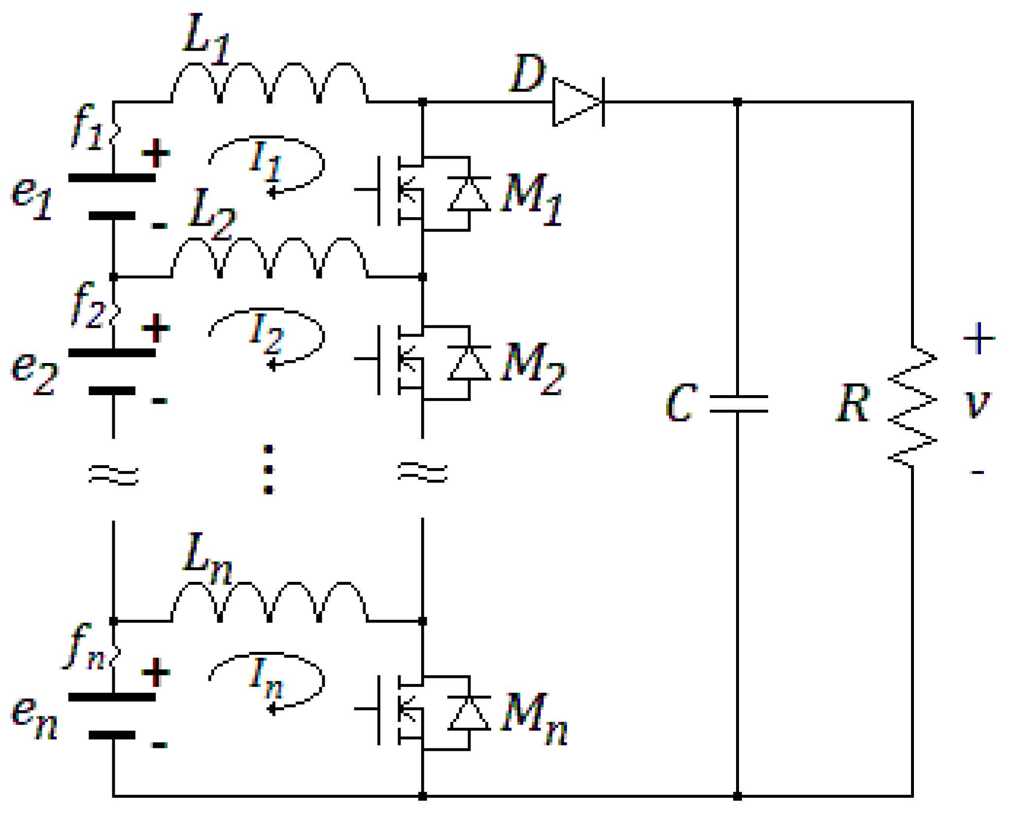
2. Modelling of the DC-DC Parallel Boost Converter

Consider the parallel DC-DC converter of Figure 1. The proposed DC-DC multiple input converter is constituted by n power sources, MOSFETs, inductors and switches, a single diode, and a single capacitor. If only a single stage is used ( n = 1 ), the converter matches with the very well-known boost converter. If n > 1 stages are designed, all the MOSFETs are switched on synchronously in continuous conduction mode (CCM), allowing the energy charging of inductors. When MOSFETs are switched off, the accumulated energy is summed to the energy of the power sources to be discharged to the capacitor and load.
On this schematic configuration, the battery cells could provide power to aid the electric service, even if:
(i)
Some, but not all, of the n cells are discharged (zero voltage).
(ii)
Some, but not all, of the n cells are in open-circuit.
(iii)
Some, but not all, of the n inductors are in open-circuit.
(iv)
Some, but not all, of the n inductors are in short-circuit.
(v)
Some, but not all, of the n MOSFETs are damaged (Drain to Source short circuit).
Note that in permanent short-circuit events (iv) and (v), the corresponding cell must be electrically isolated (by f 1 , , f n ) to avoid overheating and fire risk.
In order to demonstrate that the battery cells could provide power, even if the propositions (i)–(v) are true, a mathematical representation for the V2A converter is obtained. In later sections, a stability analysis for bounded parameter and control law output uncertainty was performed, and the stability was robust under the failure conditions (i)–(v).
Performing a Kirchhoff mesh-analysis, using I 1 ,   I 2 , ,   I n as the currents in the inductors L 1 ,   L 2 ,   ,   L n , respectively (see Figure 1), ideal components, and MOSFETs in commuted state (drain-to-source conduction), one can find the following mathematical representation:
e 1 = L 1 I ˙ 1 + L 2 ( I ˙ 1 I ˙ 2 ) e 2 = L 2 ( I ˙ 1 I ˙ 2 ) + L 3 ( I ˙ 2 I ˙ 3 ) e 3 = L 3 ( I ˙ 2 I ˙ 3 ) + L 4 ( I ˙ 3 I ˙ 4 ) e n 1 = L n 1 ( I ˙ n 2 I ˙ n 1 ) + L n ( I ˙ n 1 I ˙ n ) e n = L n ( I ˙ n 1 I ˙ n ) C v ˙ = v R
where I 1 I ˙ 1 = d I 1 d t . For the non-commuted state of the MOSFETs, the following equations are calculated:
e 1 = L 1 I ˙ 1 + L 2 ( I ˙ 1 I ˙ 2 ) + v e 2 = L 2 ( I ˙ 1 I ˙ 2 ) + L 3 ( I ˙ 2 I ˙ 3 ) + v e 3 = L 3 ( I ˙ 2 I ˙ 3 ) + L 4 ( I ˙ 3 I ˙ 4 ) + v e n 1 = L n 1 ( I ˙ n 2 I ˙ n 1 ) + L n ( I ˙ n 1 I ˙ n ) + v e n = L n ( I ˙ n 1 I ˙ n ) + v C v ˙ = i = 1 n I i v R
Introducing the control input 0 u 1 (duty cycle) and using the averaging method in continuous conduction mode ([32]):
e 1 = L 1 I ˙ 1 + L 2 ( I ˙ 1 I ˙ 2 ) + u v e 2 = L 2 ( I ˙ 1 I ˙ 2 ) + L 3 ( I ˙ 2 I ˙ 3 ) + u v e 3 = L 3 ( I ˙ 2 I ˙ 3 ) + L 4 ( I ˙ 3 I ˙ 4 ) + u v e n 1 = L n 1 ( I ˙ n 2 I ˙ n 1 ) + L n ( I ˙ n 1 I ˙ n ) + u v e n = L n ( I ˙ n 1 I ˙ n ) + u v C v ˙ = u i = 1 n I i v R
In order to find a state space representation, consider the following variable change:
x ˙ 1 = I ˙ 1 x ˙ 2 = I ˙ 1 I ˙ 2 x ˙ 3 = I ˙ 2 I ˙ 3 x ˙ n = I ˙ n 1 I ˙ n x ˙ n + 1 = v
Then, the state space representation is:
x ˙ 1 = 1 L 1 i = 1 n e i + 1 L 1 u x n + 1 x ˙ 2 = 1 L 2 i = 2 n e i + 1 L 2 u x n + 1 x ˙ 3 = 1 L 3 i = 3 n e i + 1 L 3 u x n + 1 x ˙ n = 1 L n i = n n e i + 1 L n u x n + 1 x ˙ n + 1 = 1 C u i = 0 n 1 ( n i ) x i + 1 x n + 1 R C
For instance, and in order to illustrate the obtaining of the model, consider n = 3 ; the two switched configurations shown in Figure 2 are possible.
The I 1 mesh analysis for commuted MOSFETs (Figure 2a) reads:
e 1 = L 1 I ˙ 1 + L 2 ( I ˙ 1 I ˙ 2 )
where I 1 I ˙ 1 = d I 1 / d t . For meshes I 2 and I 3 one has:
e 2 = L 2 ( I ˙ 2 I ˙ 1 ) + L 3 ( I ˙ 2 I ˙ 3 ) = L 2 ( I ˙ 1 I ˙ 2 ) + L 3 ( I ˙ 2 I ˙ 3 )
and
e 3 = L 3 ( I ˙ 3 I ˙ 2 ) = L 3 ( I ˙ 2 I ˙ 3 )
The mesh analysis in the right side is:
C v ˙ = v R
For a non-conducting state, one can easily obtain a set of equations if new meshes are set, as illustrated in Figure 2b for the I 1 mesh. Using the variable change of Equation (4) and the averaging method one has:
x ˙ 1 = 1 L 1 ( e 1 + e 2 + e 3 ) + 1 L 1 u x 4 x ˙ 2 = 1 L 2 ( e 2 + e 3 ) + 1 L 2 u x 4 x ˙ 3 = 1 L 3 e 3 + 1 L 3 u x 4 x ˙ 4 = 1 C u ( 3 x 1 + 2 x 2 + x 3 ) + x 4 R C
In this scenario, from equations (10) and (4), the steady-state output voltage is:
v = ( e 1 + e 2 + e 3 ) / u

3. Stability Analysis

The main objective of the V2A converter presented in this article, is to keep the output voltage, despite variations in components and even its failures. For that purpose, one can obtain a second-degree differential equation for the output voltage with the form:
z ˙ 1 = α u 2 z 2 β z 1 + γ u z ˙ 2 = z 1
where
z 1 = x ˙ n + 1 z 2 = x n + 1
and α ,   β , and γ are positive parameters calculated as follows:
α = i = 1 n n + 1 i L i C β = 1 R C γ = i = 1 n e i ( j = i i n + 1 j L j C )
For instance, with n = 2 :
α = 2 L 1 C + 1 L 2 C β = 1 R C γ = 2 e 1 L 1 C + ( 2 L 1 C + 1 L 2 C ) e 2
In the following, the system (12) is modelled as a polytopic system with uncertain parameters α ,   β , γ , and u , and posteriorly analyzed for stability using a common Lyapunov function (CLF), and in this way ensuring stability, even with arbitrarily fast changing parameters and any u . This is because every bounded control law stabilizes the system, and this can be in sliding modes, classic, fuzzy, and other controllers.
The system (12) written on its matrix form is:
z ˙ = A z + B
where
A = [ β α u 2 1 0 ]   and   B = [ γ u 0 ]
Since u is considered a time varying parameter, the variable change
y 1 = z 1 y 2 = α u 2 z 2 + γ u
allows to nullify the drift term to obtain:
y ˙ = A y
where
A = [ β α u 2 α u 2 0 ]
Consider parametric variation within known ranges (it is already known that 0 u u m a x , where u m a x is the maximum pulse width modulation (PWM) duty cycle, will be 0.85 at most in a real application) denoted by an underline for the minimum value and by an overline for the maximum value, as follows:
y ˙ = A ( t ) y
with
0 a 11 _ β ( t ) a 11 ¯
0 a 21 _ α ( t ) u 2 ( t ) a 21 ¯
The system (17) can be written as a polytopic, simplice system [33]:
y ˙ = θ 1 A 1 y + θ 2 A 2 y + θ 3 A 3 y + θ 4 A 4 y
where θ i = 1 , θ i 0 , and the vertexes are
A 1 = [ a 11 _ a 12 _ a 12 _ 0 ] ,       A 2 = [ a 11 _ a 12 ¯ a 12 ¯ 0 ] ,  
A 3 = [ a 11 ¯ a 12 _ a 12 _ 0 ] ,       A 4 = [ a 11 ¯ a 12 ¯ a 12 ¯ 0 ] .
From [34], the quadratic stability of the system (19) is ensured if there exists a common symmetric positive definite matrix P , such that the Lyapunov equations
P A i + A i T P 0
holds i with θ i = 1 . This is, the left side matrix sum of (20) must be a Hurwitz’ matrix with:
P = [ p 1 p 2 p 2 p 3 ]
For simplicity, consider arbitrary but bounded values 0 a 11 _ a a 11 ¯ and 0 a 21 _ b a 21 ¯ , then every vertex can be represented as:
A v = [ b a a 0 ]
The Lyapunov equation for any vertex must be negative definite
P A v + A v T P 0
and its eigenvalues are
λ 1 , 2 = b p 1 ± a 2 p 1 2 + 4 a 2 p 2 2 + a 2 p 3 2 + b 2 p 1 2 + b 2 p 2 2 2 a 2 p 1 p 3 2 a b p 1 p 2 2 a b p 2 p 3
Since the eigenvalues can only be real numbers, the only possibility that there is a positive eigenvalue is when the root is positive; therefore, with p 1 = p 3 = 1 , it is enough to ensure that:
b 2 > ( 4 a 2 p 2 2 4 a b p 2 + b 2 p 2 2 + b 2 ) 2
which reduces to
p 2 < 4 a b 4 a 2 + b 2
On the other hand
P = [ 1 p 2 p 2 1 ] 0
which reduces to
p 2 < 1
Hence, for every vertex, one has that is enough to fulfill:
p 2 < 4 a 11 _ a 21 _ 4 a 11 2 _ + a 21 2 _
Since p 2 can be an arbitrarily small positive number, one can always found p 2 and hence a CLF, concluding the robust stability under bounded parameter uncertainty and bounded control input u ( t ) .

4. Robust Stability under Failure Conditions

In this section, is verified the previous stability analysis under the failure conditions (i)–(v).

4.1. Some Discharged Cells

If any cell is discharged, its voltage tends to zero and, viewed analytically, a variation occurs in the sigma parameter of the system (7) that does not affect the stability properties. The equilibrium point is altered so that an appropriate control in closed loop will demand more current from the rest of the cells. In the extreme case that only one cell remains charged and the rest is discharged, it is possible that the control law is not able to reach a reference value. That is, the control input is limited by the physical characteristics inherent to the components. However, the stability properties shown in this paper are retained, while the controller must ensure appropriate convergence as much as possible.

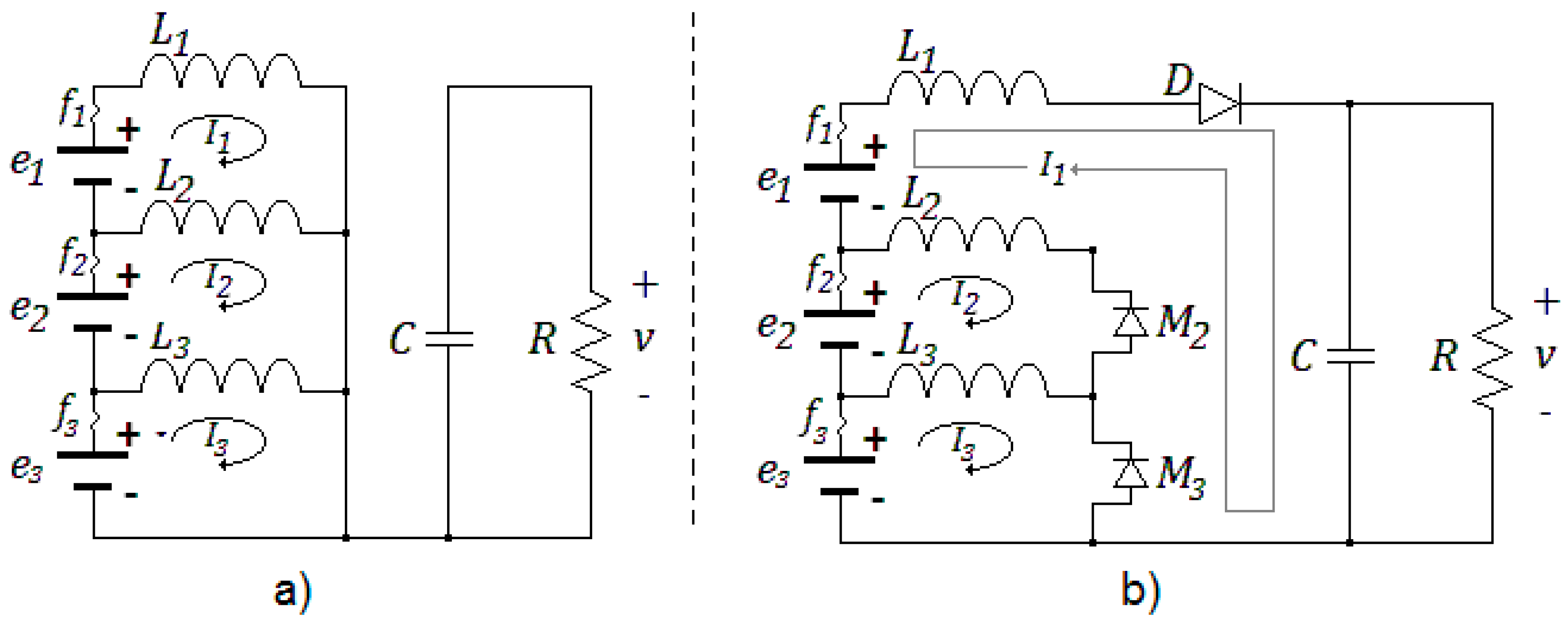
4.2. Cells in Open Circuit

Two main possibilities of a cells in open circuit are possible:
  • The first ( e 1 ) cell is in open circuit. In this case, the circuit behaves has some of m = n 1 cells. The model remains without structural modification, and the stability properties are conserved; moreover, it is easy to demonstrate that the CLF found for n cells is also valid for m cells, and therefore the stability property is retained, even during the switching between the models.
  • The k -th cell ( e 2 ,   e 3 ,   , or e n ) is in open circuit. In such a case, the circuit behaves as some of m = n 1 , where the inductance in the upper mesh is now L e q = L k 1 + L k . This change is now considered within the parameter variation ranges of the model, without structural modification or changes on the stability properties.
With any combination of the above of this subsection, as long as at least one mesh is operating, is possible to keep feeding the load.

4.3. Some but not All of the n Inductors are in Open Circuit

Two main possibilities of an inductor in open circuit are possible:
  • The first inductor ( L 1 ) is in open circuit. In this case, the circuit behaves has some of m = n 1 cells. The model remains without structural modification and the stability properties are conserved; moreover, it is easy to demonstrate that the CLF found for n cells is valid also for m cells, and therefore the stability property is retained even during switching between the models.
  • The k -th inductor ( L 2 ,   L 3 ,   ,   o r   L n ) is in open circuit. In such case, the circuit behaves as some of m = n 1 cells, where the equivalent voltage source in the respective mesh is now e e q = e k 1 + e k . This change is now considered within the parameter variation ranges of the model without structural modification neither changes on the stability properties.
With any combination of the above of this subsection, as long as at least one mesh is operating, is possible to keep feeding the load.

4.4. Some but not All of the n Inductors are in Short Circuit

If the k -th inductor is in short circuit, the current in the e k voltage source rises to open the f k fuse. Such resulting circuit coincides with the scenario analyzed in Section 4.2.

4.5. Drain to Source Short Circuit

If the k -th MOSFET is in short circuit, the current in the e k voltage source rises to open the f k fuse. Such resulting circuit coincides with the scenario analyzed in Section 4.2.

4.6. Combinations of Failure Events
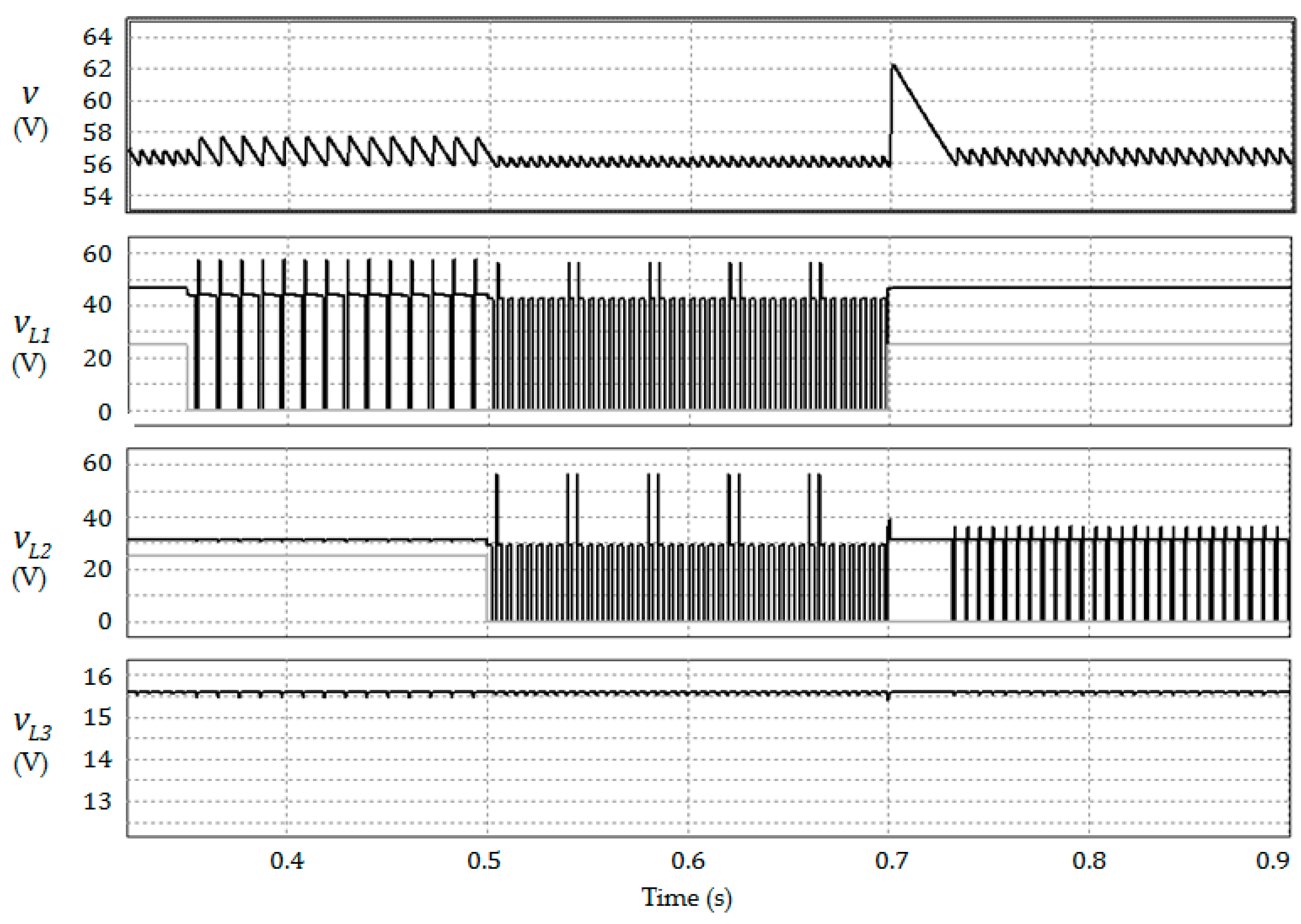
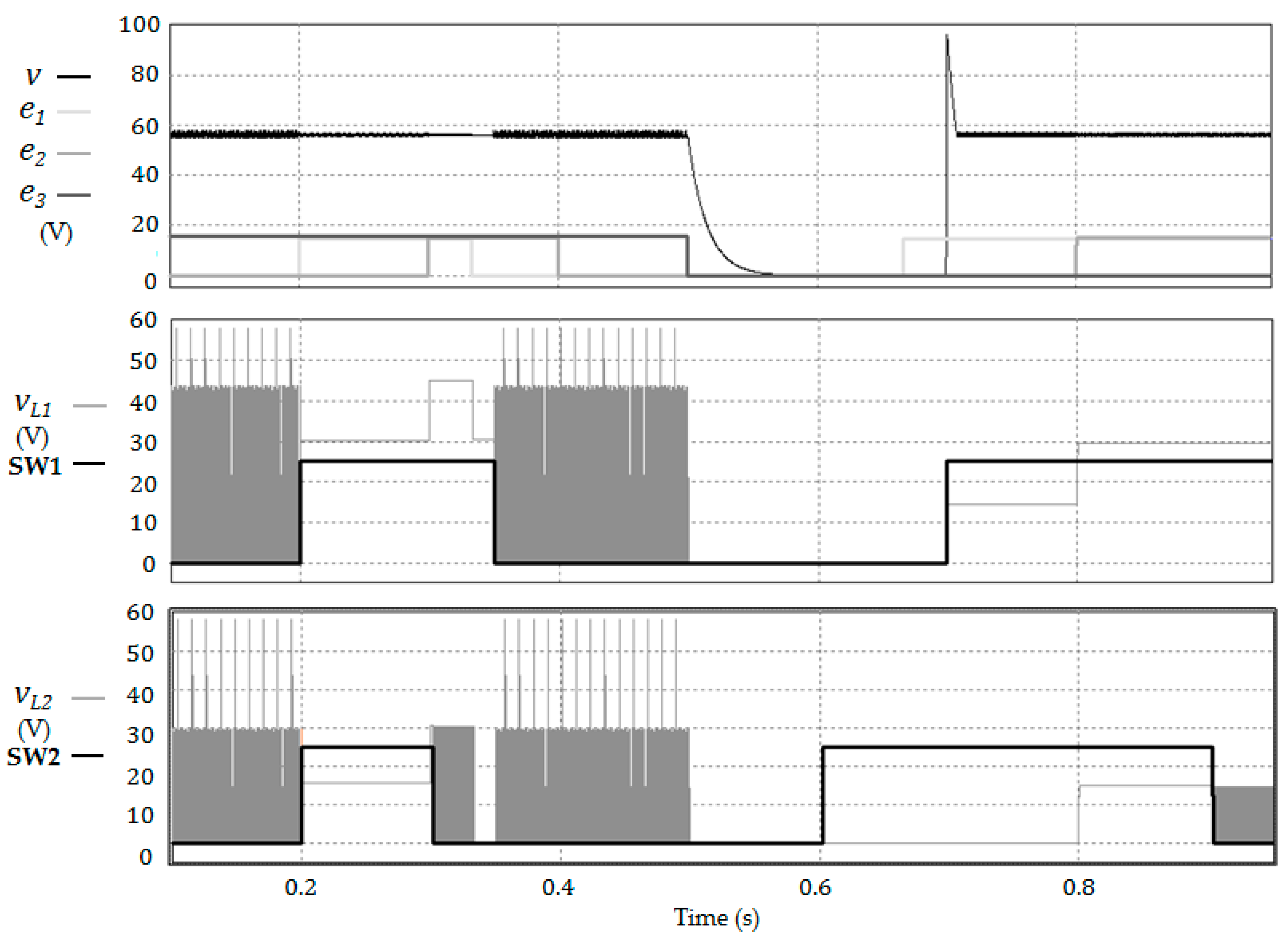
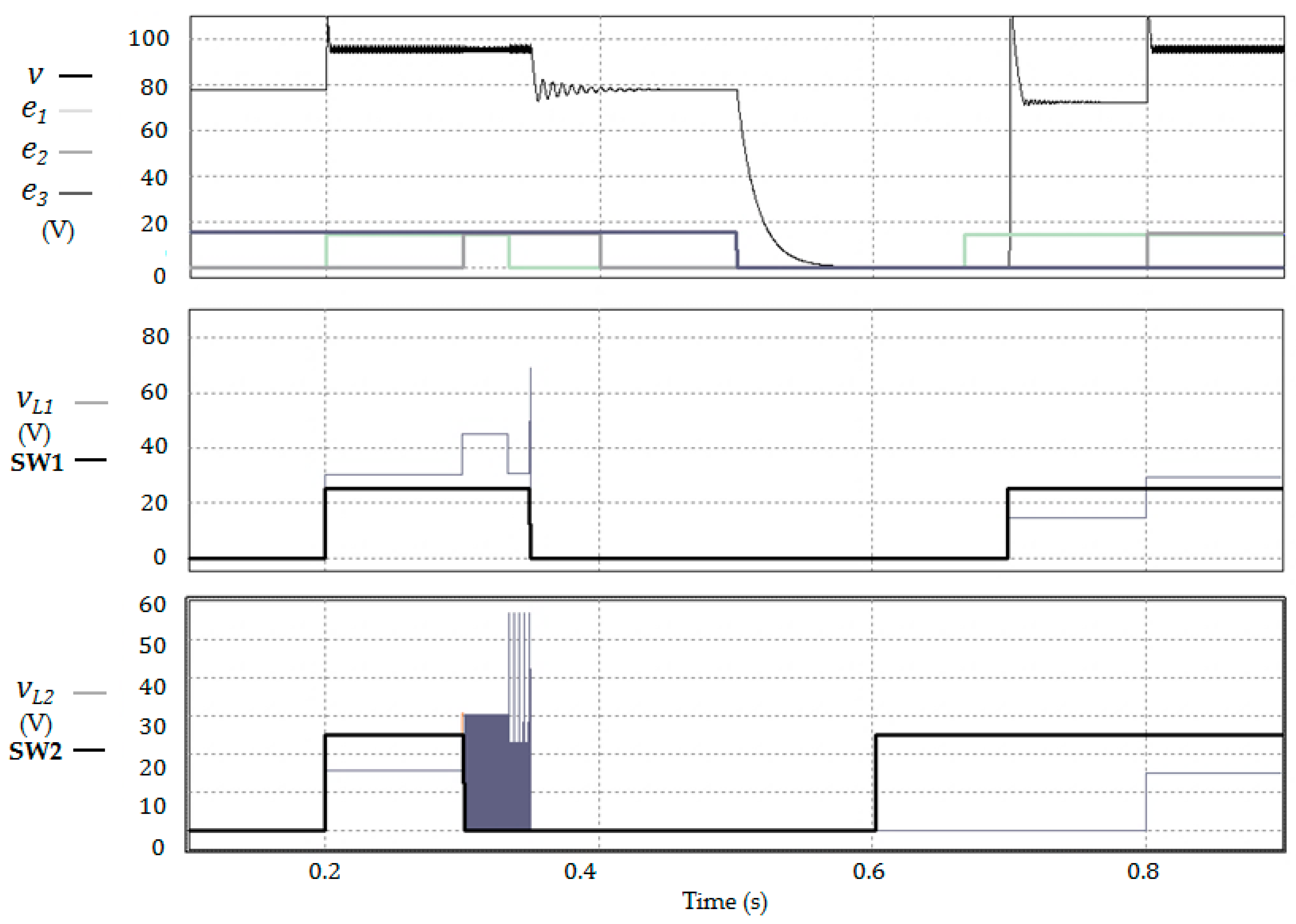
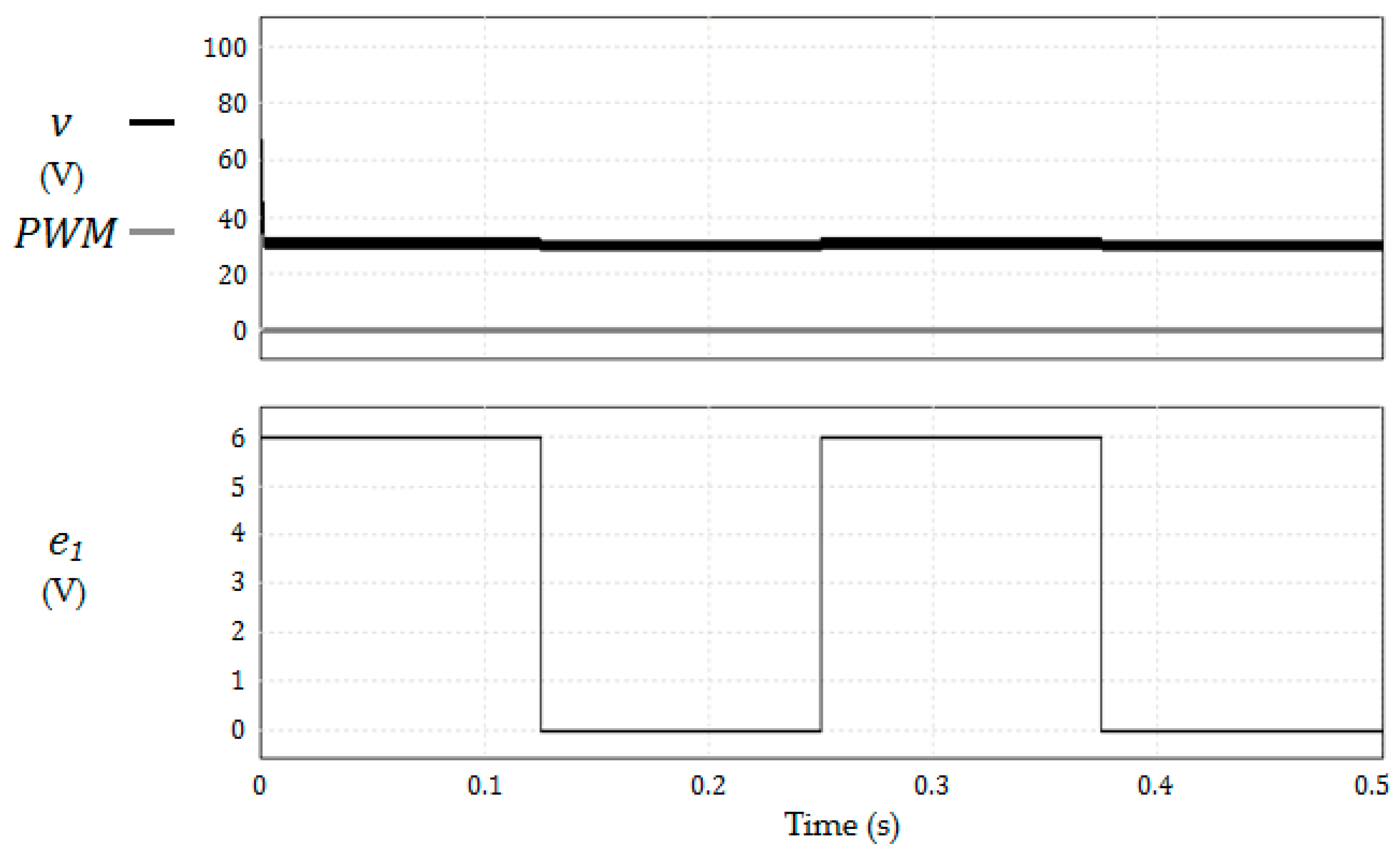
Note that the V2A converter shown in this paper can provide energy to the load, as long as one feeding mesh is operative and the stability properties are preserved; however, it is possible that the control law is not able to reach a reference value. That is, the control input is limited by the physical characteristics inherent to the components.
The previous analysis allows us to infer that compared to other configurations of electronic power converters, in this configuration the sources can be connected in series (they do not need to be isolated) while their continuous operation is guaranteed, despite failures in the inductors, MOSFETS, or even power supplies, without the need for external fault detection circuitry. In addition, under this configuration voltage regulation is achieved simultaneously by means of simple controllers, such as the proportional integral (PI), while other configurations require more complex techniques such as the master-slave. Furthermore, it is demonstrated that the stability in closed loop is guaranteed, despite changes in parameters and component failures.
It is worth mentioning that a finer regulation scenario should include the programming of PI controller gains or advanced control techniques. In addition, the behavior of the configuration in discontinuous conduction mode (DCM) should be studied as it can offer advantages over the CCM. Such scenarios are not the subject of this document and are left for future work.

5. Simulations

In this section, the converter behavior under failure conditions is illustrated (i)–(v). For this, Software for Power Electronics Simulation (PSIM) is used, with a classic PI controller, n = 3 , L i = 1 mH, C = 200 μF, R = 144 Ω, e 1 = e 2 = e 3 = 15.6 V, a PWM frequency f = 40 kHz, and a maximum duty cycle of 80 %.

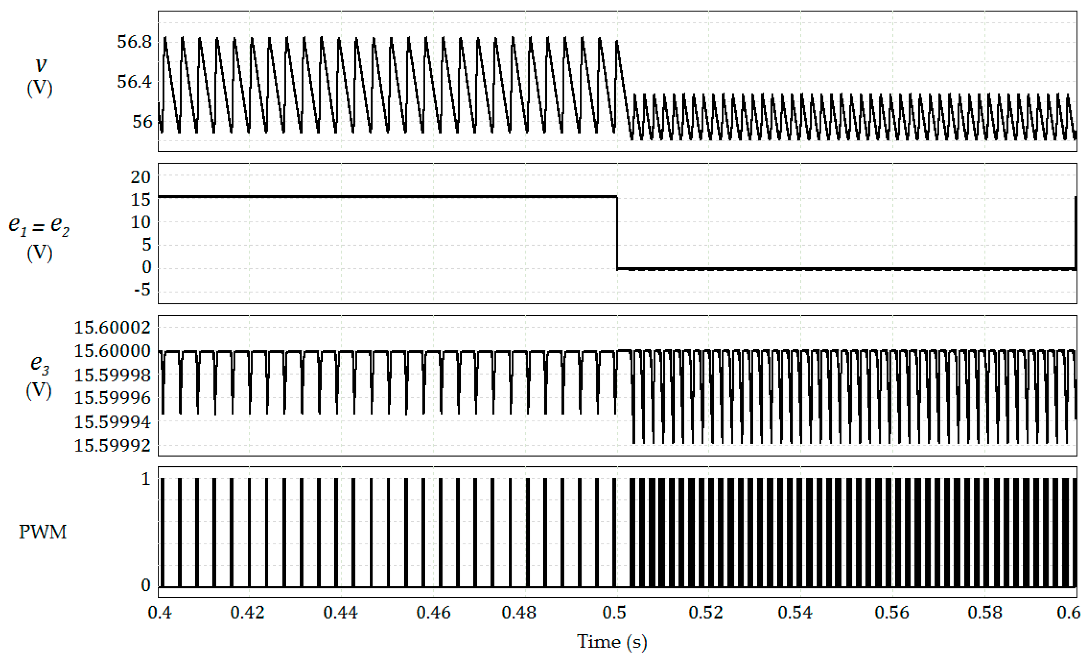
5.1. Some Discharged Cells

Figure 3 shows the dynamic behavior of the output voltage, source voltages, and the PWM duty cycle respectively. For a voltage drop in e 1 and e 2 from their nominal voltage to zero volts at 0.1 s, with a 56 V reference for the PI controller, the output voltage is clearly stable, and the PI controller can regulate the output; note that the PI controller can be tuned for a desired output response.

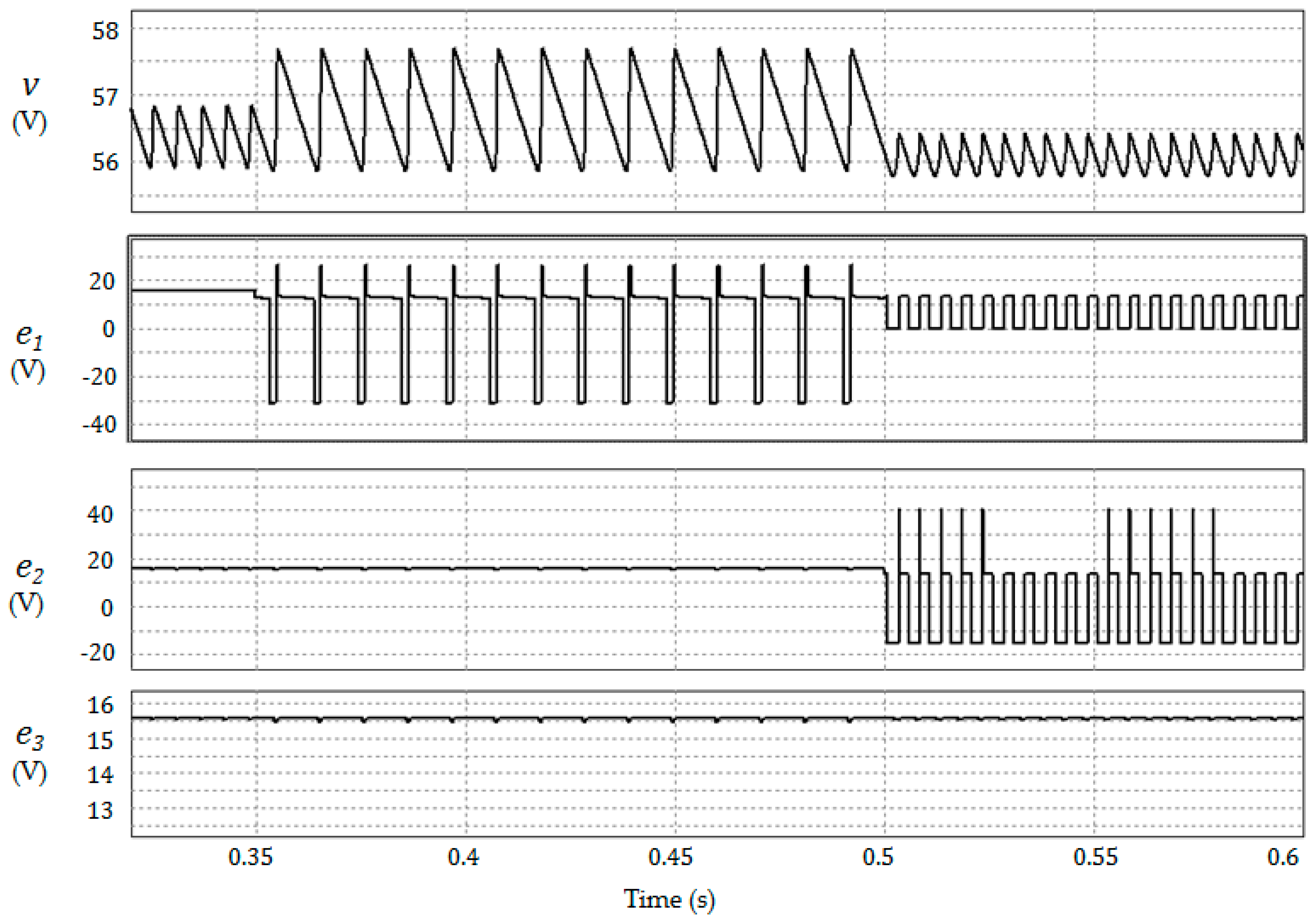
5.2. Cells in Open Circuit

Figure 4 shows the dynamic behavior of the output voltage and the source voltages for an open circuit in the e 1 cell at 0.35 and in the e 2 cell at 0.5 s. That is, an internal disconnection in the cell is emulated. With a 56 V reference for the PI controller, the output voltage is clearly stable and the PI controller can regulate the output.

5.3. Some but not All of the n Inductors are in Open Circuit

Figure 5 shows the dynamic behavior of the output voltage and the voltages on the inductors ( v L 1 to v L 3 ), respectively. In this graphic, the inductor L 1 is switched to open circuit at 0.35 s, and reconnected at 0.7 s, while the inductor L 2 is switched to open circuit at 0.5 s. With a 56 V reference for the PI controller, the output voltage is clearly stable, and the PI controller can regulate the output.
The inductor model used in PSIM is ideal and allows for the preservation of energy (in real life the energy loss is faster) that is summed to that of e 1 when re-connected at 0.7 s. It is recommended to discharge the inductor for a fine and smooth switch, if it is necessary to avoid this transient.

5.4. Some but not All of the n Inductors are in Short Circuit

If the k -th inductor is in short-circuit, the current in the e k voltage source rises to open the f k fuse. The resulting circuit coincides with the simulation presented in Section 5.2.

5.5. Drain to Source Short Circuit

If the k -th MOSFET is in short circuit, the current in the e k voltage source rises to open the f k fuse. The resulting circuit coincides with the scenario analyzed in Section 5.2.

5.6. Combinations of Failure Events

Figure 6 shows the dynamic behavior for the parallel V2A converter under severe failure conditions. The parameters are changed to L 1 = 0.1 mH, L 2 = 1 mH, L 3 = 0.5 mH, C = 100 μF, intermittent e i sources with peak voltages of 14.5 ,   15.0 , and 15.6 V, and intermittent switches to open each inductor as depicted in Figure 6.
The upper plot of Figure 6 shows the output voltage with a PI controller, closed loop system with reference set to 56 V. Note that as long as a power mesh is operating, it is possible to maintain the output voltage at its desired level, even in the case of various faults in the rest of the meshes and variations in the nominal values of the parameters (shown in the two lower plots of the figure).
In Figure 7, the previous simulation is repeated with a reference set to 95 V. Since the control input is limited by the physical characteristics inherent to the components, the controller is not able to reach the reference value with a single source mesh operating in the period from 0.35 to 0.5 s. However, the stability properties are preserved independently of the fact that the controller and the design of the respective power grid do not achieve the desired output voltage value.
If the k -th MOSFET is in short circuit, the current in the e k voltage source rises to open the f k fuse. The resulting circuit coincides with the scenario analyzed in Section 5.2.

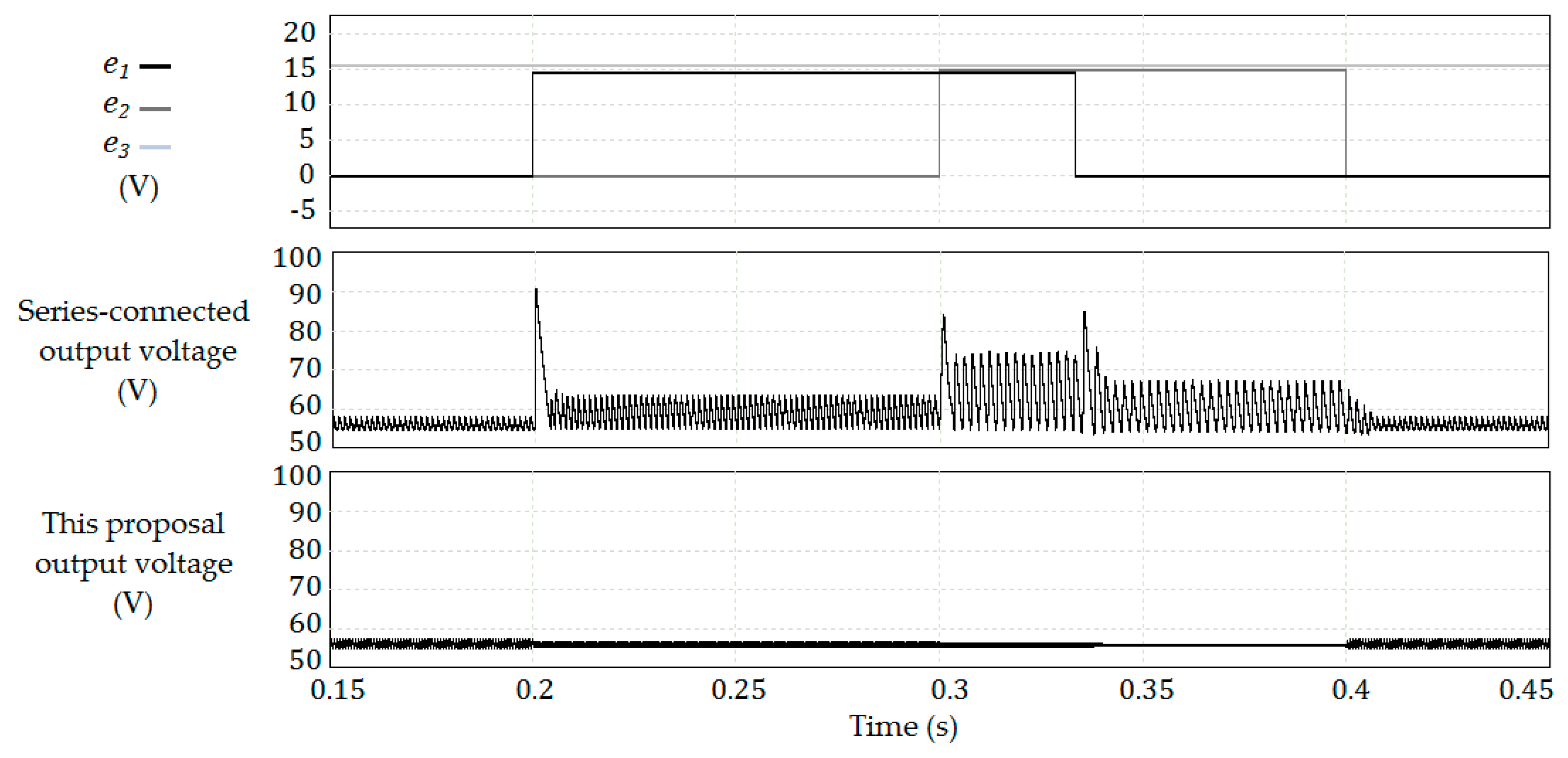
5.7. Boost Series-Connected Comparison
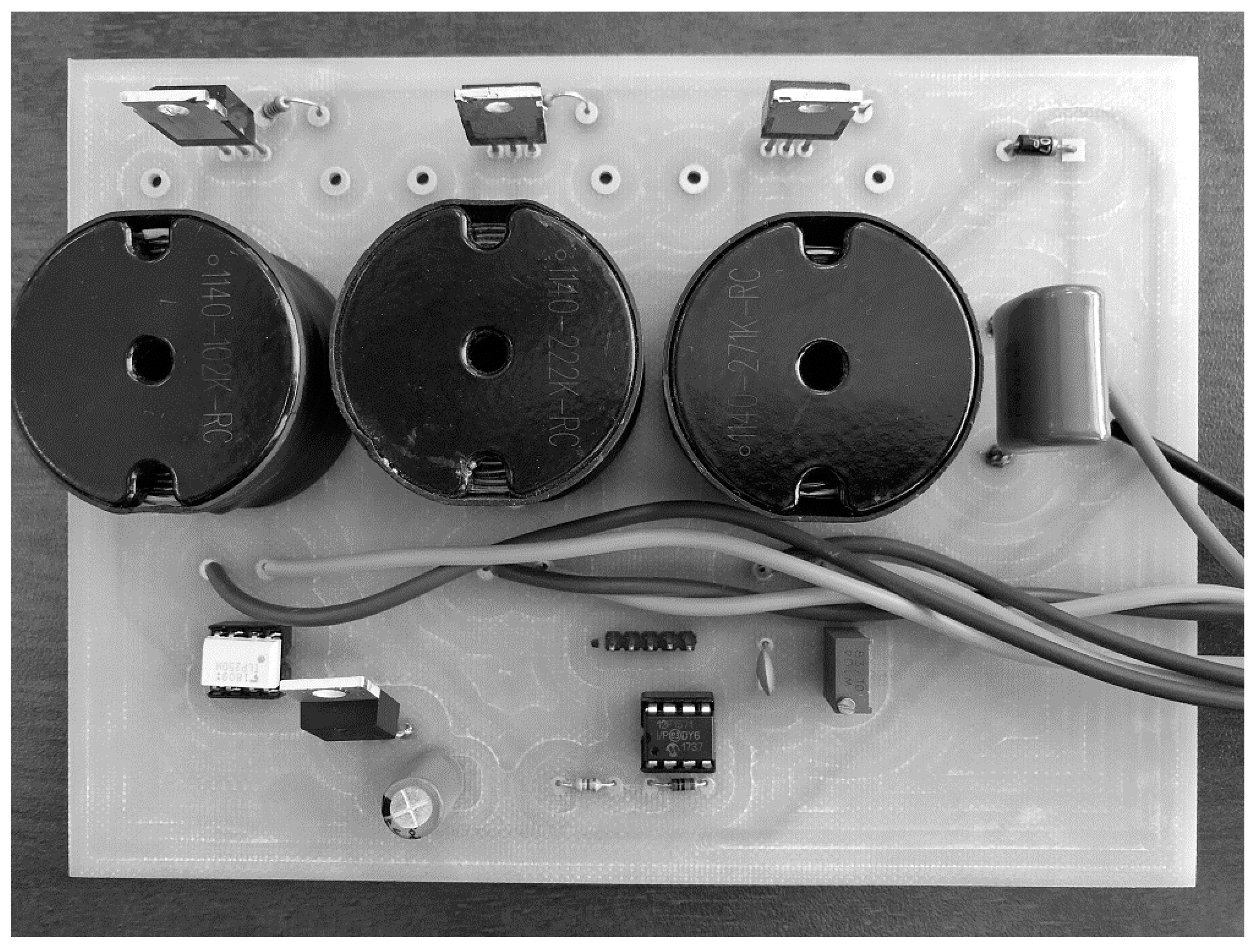
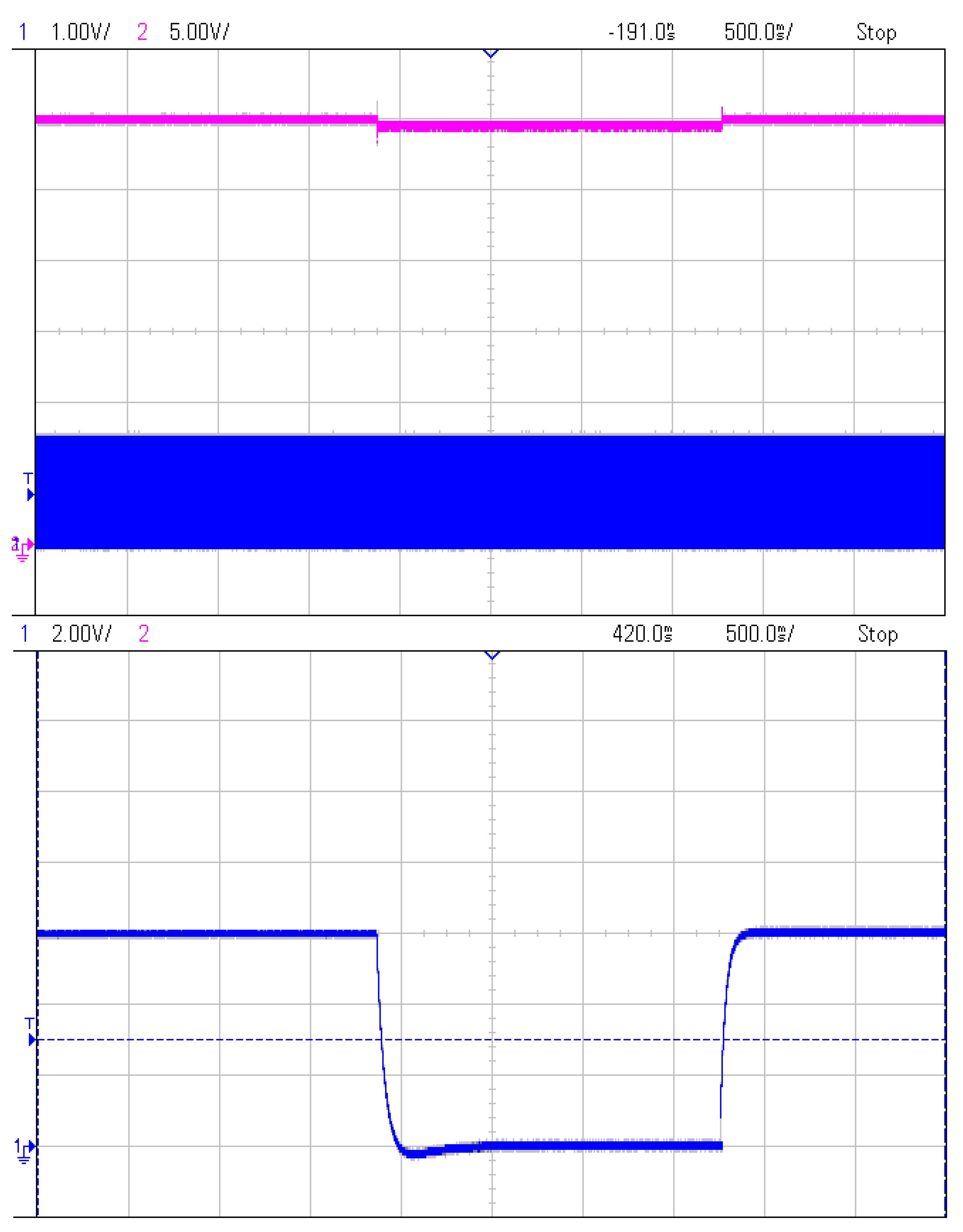
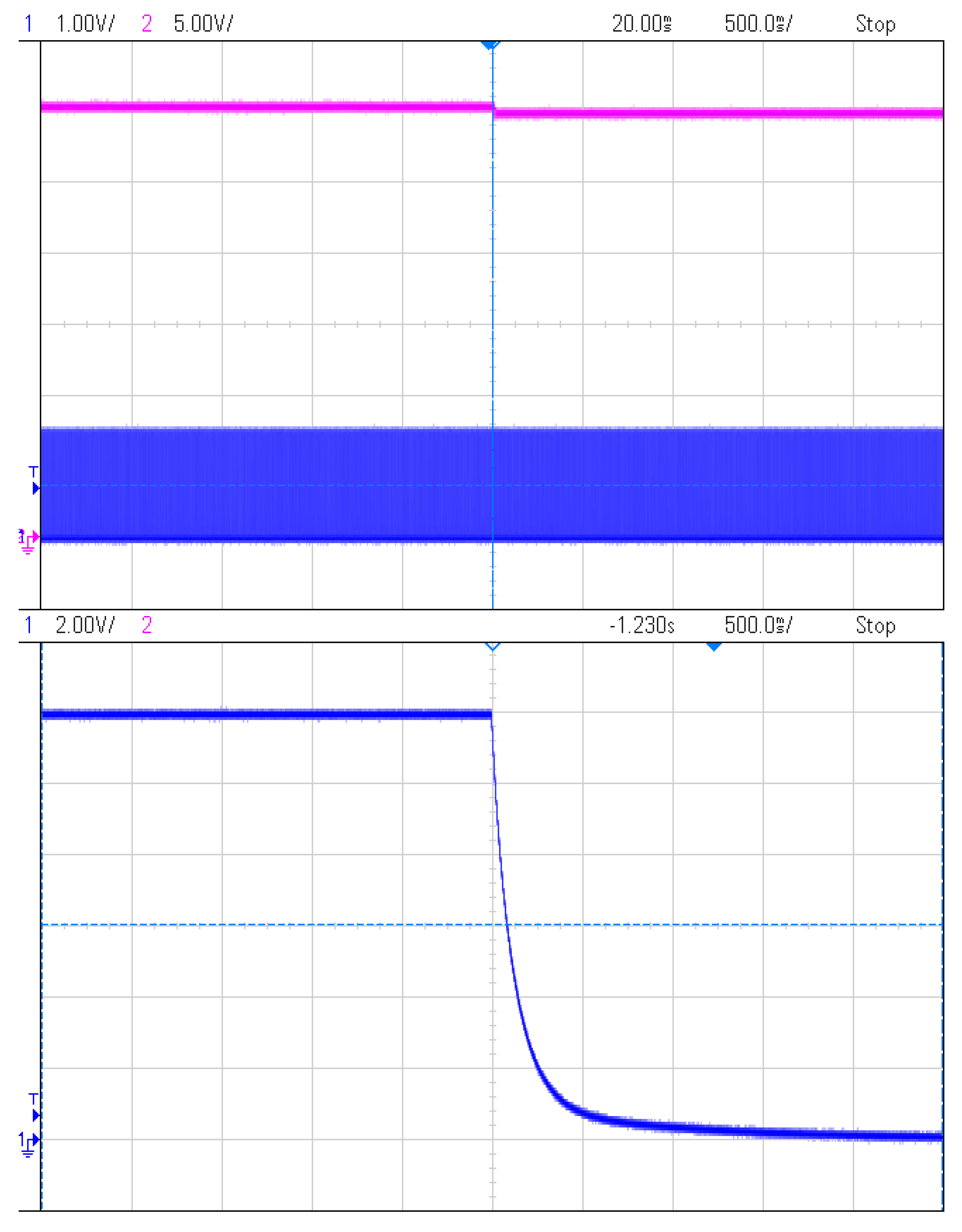
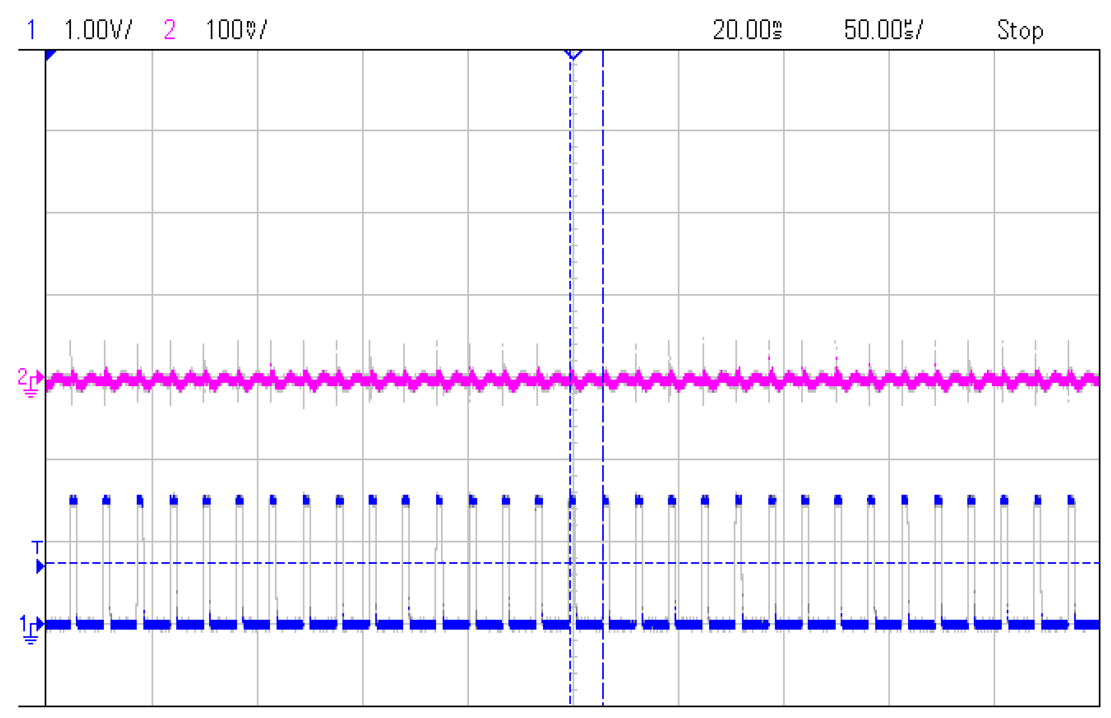
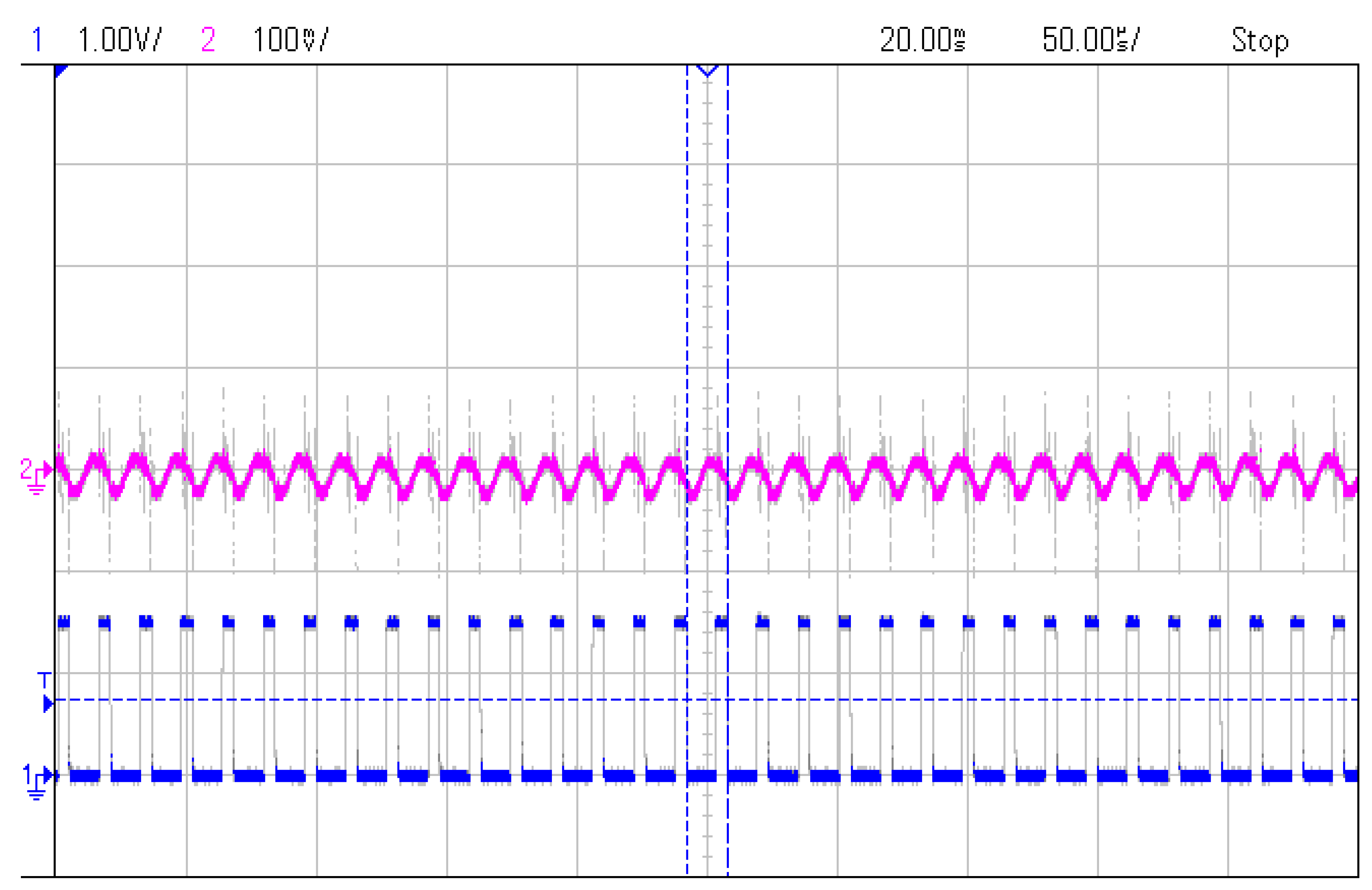
The configuration presented in [30,31] (illustrated in Figure 8 with n = 3 ) could provide similar robustness characteristics to the converter proposed in this paper. However, a first advantage of the proposal of this paper with respect to a series-connected boost, is that the power sources can be connected in series, instead of an isolated-sources configuration. A second advantage is the reduced number of components in this proposal. A third advantage was found in terms of voltage regulation (PI closed-loop dynamic response), since it is easy to show that the output function of series connected boost converters is the sum of n duty cycles to output voltage transfer functions, while, from Equation (12), one can obtain a single second order transfer function, even if the parameters are distinct between stages.
In order to illustrate the aforementioned results, Figure 9 shows a comparison of a PI, closed loop voltage regulation for three series-connected boost converters against the three-stage proposal of this paper. In this simulations L a = L 1 = 100 μH, L b = L 2 = 1 mH, L c = L 3 = 500 μH, e a = e 1 = 14.5 V, e b = e 2 = 15 V, e c = e 3 = 15.6 V, and all capacitors are 100 μF with a 144 Ω load. The power sources are turned on-off intermittently, as shown in the upper plot, and a 56 V set point is used. For the series-connected configuration, the tuning of the PI controller is complicated; regardless of whether you use a PI per stage or a single PI, simultaneous or sequential triggering, an acceptable behavior is hard to obtain (middle plot); for such cases, different control strategies are recommended (see [6,7,8]). In contrast, for the proposed circuit topology, the tuning is very simple and the response is more smooth (bottom plot).

6. Experiments

The proposed parallel DC-DC converter of Figure 1 was implemented in order to show an experimental behavior in la ow power level (semi-experimental tests indicate that the scalability at higher powers is feasible). The parameters/values are selected arbitrarily (according to laboratory availability) to show that steady state operation does not depend largely on parametric variation within reasonable ranges, and are verified in Section 3. Figure 10 shows a picture of the printed circuit board (PCB), with L 1 = 1 mH, L 2 = 2.2 mH, L 3 = 0.27 mH, C = 3.9 μF, R = 444 Ω, e 3 = 12 V, e 2 = 10 V, and e 1 = 6 V. A PIC12F1571 microcontroller model from Microchip is used to generate the PWM signal, perform analog to digital conversion, and implement the PI control; Although it is shown on the PCB, the description of the mentioned device was omitted. In the new version of the document, the device used is described, along with some other implementation details. As can be noticed, the parameters were intentionally selected differently. The switching frequency was set to 60 kHz with a set point of 30 V for the PI controller.
Figure 11 shows the output voltage, the PWM activation signal (10:1 scaled), and the voltage e 1 in descending order for the first experiment (oscilloscope captures). While the voltage was set to zero (disconnected from the source), then short-circuited and reconnected again, it is easy to note that the output voltage was stable with an error of 1 V. Additionally, the voltage in e 2 was set to open and then short-circuited so that the converter was operating only with e 3 ; the experimental behavior is shown in Figure 12, similarly to Figure 11.
Figure 13, Figure 14 and Figure 15 show the output ripples obtained for nominal operation, e 2 drop, and e 3 drop respectively. It can be noticed that the ripple increased considerably as the fall in the voltages of the other sources is greater.
Figure 16 shows the corresponding simulation results with the experimental test parameters and short-circuit failure events for the sake of completeness.

7. Discussion

Experiments showed that the current is higher in the mesh with higher input voltage; this could be detrimental in applications where a single power supply supplies the power and one stage is overloaded more than the others are. In the case of the converter for V2A applications presented in this paper, this is not harmful, and represents a benefit, since there are n > 1 cells instead a single one, and it is sought to discharge first the cell that has the higher SoC.
On the other hand, exploring the use of P-channel MOSFETs with isolated activation stages to avoid its coupling is recommended. Likewise, the tuning in the case of classical controllers could be adjusted to decrease the ripple of the output voltage or obtain a desired transient response, in case of the failure of one or more cells. As mentioned above, it is not the purpose of this document to present a specific controller for the proposed converter, but rather to demonstrate its fault tolerance and stability to changes in the parameters, including the control input.
It is worth mentioning that an increase in size and weight is justified by the type of application; moreover, while electronic devices can be encapsulated on a single chip, the high frequency inductors are relatively small—even more so those built with advanced core materials, such as the nanocrystal. For example, a ferrite (regular) inductor of 1 mH and 10 A of current would allow about 2.2 kW operating at 220 V (effective) with a weight of 450 grams and about 190 cm3 (Hammond 157D).

8. Conclusions

This paper proposed a new DC-DC converter for a new scheme of electric vehicles to aid-services. The analytic, numeric, and experimental results showed that the proposed converter is very robust against battery/cell and components failures, unequal states of charge, variations in parameters, and control design errors. The stability analysis demonstrated the robust global stability against bounded parameter variations by a common Lyapunov function, and it can be easily extended to hard switching between operation modes.

Funding

This research received no external funding.

Acknowledgments

This work was supported by the CONACYT under Grant Cathedra ID 4155. The author thanks to Alma Pamela Rodríguez Huerta for her help on image processing.

Conflicts of Interest

The author declares no conflict of interest for this paper.

References

  1. Ganesan, S.; Padmanaban, S.; Varadarajan, R.; Subramaniam, U.; Mihet-Popa, L. Study and analysis of an intelligent microgrid energy management solution with distributed energy sources. Energies 2017, 10, 1419. [Google Scholar] [CrossRef] [Green Version]
  2. Noel, L.; Rubens, G.Z.; Kester, J.; Sovacool, B.K. Vehicle-to-Grid: A Sociotechnical Transition Beyond Electric Mobility; Springer: Cham, Switzerland, 2019; pp. 1–85. ISBN 978-3-030-04863-1. [Google Scholar]
  3. Corchero, C.; Sanmarti, M. Vehicle-to-Everything (V2X): Benefits and Barriers. In Proceedings of the IEEE International Conference on the European Energy Market, Łódź, Poland, 27–29 June 2018. [Google Scholar]
  4. Wang, B. Intelligent Control and Power Flow Optimization of Microgrid: Energy Management Strategies. Ph.D. Thesis, Sciences pour l’ingénieur, Compiègne, France, 2013. [Google Scholar]
  5. Jovanovic, M.M.; Crow, D.E.; Fang-Yi, L. A novel, low-cost implementation of “democratic” load-current sharing of paralleled converter modules. IEEE Trans. Power Electron. 1996, 11, 604–611. [Google Scholar] [CrossRef]
  6. Shebani, M.M.; Iqbal, T.; Quaicoe, J.E. Synchronous Switching for Parallel-Connected DC-DC Boost Converters. In Proceedings of the IEEE Electrical Power and Energy Conference, Saskatoon, SS, Canada, 22–25 October 2017. [Google Scholar]
  7. Grbovic, P.J. Master/slave control of input-series-and output-parallel-connected converters: Concept for low-cost high-voltage auxiliary power supplies. IEEE Trans. Power Electron. 2009, 24, 316–328. [Google Scholar] [CrossRef]
  8. Choudhary, V.; Ledezma, G.; Ayyanar, R.; Button, R.M. Fault tolerant circuit topology and control method for input-series and output-parallel modular DC-DC converters. IEEE Trans. Power Electron. 2008, 23, 402–411. [Google Scholar] [CrossRef]
  9. Al-Sheikh, H.; Bennouna, O.; Hoblos, G.; Moubayed, N. Modeling, Design and Fault Analysis of Bidirectional DC-DC Converter for Hybrid Electric Vehicles. In Proceedings of the IEEE 23rd International Symposium on Industrial Electronics, Istanbul, Turkey, 1–4 June 2014. [Google Scholar]
  10. Lee, Y.; Emadi, A. Phase Shift Switching Scheme for DC/DC Boost Converter with Switches in Parallel. In Proceedings of the IEEE Vehicle Power and Propulsion Conference, Heilongjiang, China, 3–5 September 2008. [Google Scholar]
  11. Stala, R.; Waradzyn, Z.; Penczek, A.; Mondzik, A.; Skała, A. A switched-capacitor DC–DC converter with variable number of voltage gains and fault-tolerant operation. IEEE Trans. Ind. Electron. 2018, 66, 3435–3445. [Google Scholar] [CrossRef]
  12. Mohammadpour, A.; Parsa, L.; Todorovic, H.M.; Lai, R.; Datta, R.; Garces, L. Series-input parallel-output modular-phase dc–dc converter with soft-switching and high-frequency isolation. IEEE Trans. Power Electron. 2015, 31, 111–119. [Google Scholar] [CrossRef]
  13. Shahbazi, M.; Jamshidpour, E.; Poure, P.; Saadate, S.; Zolghadri, M.R. Open-and short-circuit switch fault diagnosis for nonisolated DC–DC converters using field programmable gate array. IEEE Trans. Ind. Electron. 2012, 60, 4136–4146. [Google Scholar] [CrossRef] [Green Version]
  14. Ribeiro, E.; Cardoso, A.J.M.; Boccaletti, C. Fault-tolerant strategy for a photovoltaic DC–DC converter. IEEE Trans. Power Electron. 2012, 28, 3008–3018. [Google Scholar] [CrossRef]
  15. Guilbert, D.; Guarisco, M.; Gaillard, A.; N’Diaye, A. FPGA based fault-tolerant control on an interleaved DC/DC boost converter for fuel cell electric vehicle applications. Int. J. Hydrogen Energy 2015, 40, 15815–15822. [Google Scholar] [CrossRef]
  16. Choi, B. Comparative study on paralleling schemes of converter modules for distributed power applications. IEEE Trans. Ind. Electron. 1998, 45, 194–199. [Google Scholar] [CrossRef]
  17. Ribeiro, E.; Cardoso, A.J.M.; Boccaletti, C. Open-circuit fault diagnosis in interleaved DC–DC converters. IEEE Trans. Power Electron. 2013, 29, 3091–3102. [Google Scholar] [CrossRef]
  18. Jamshidpour, E.; Shahbazi, M.; Poure, P.; Gholipour, E.; Saadate, S. Fault Tolerant Operation of Single-Ended Non-Isolated DC-DC Converters Under Open and Short-Circuit Switch Faults. In Proceedings of the European Conference on Power Electronics and Applications, Lille, France, 4 September 2013. [Google Scholar]
  19. Jamshidpour, E.; Shahbazi, M.; Poure, P.; Gholipour, E.; Saadate, S. FPGA Based Fault Detection and Fault Tolerance Operation in DC-DC Converters. In Proceedings of the IEEE International Symposium on Power Electronics, Electrical Drives, Automation and Motion, Ischia, Italy, 18–20 June 2014. [Google Scholar]
  20. Jamshidpour, E.; Poure, P.; Gholipour, E.; Saadate, S. Single-switch DC–DC converter with fault-tolerant capability under open-and short-circuit switch failures. IEEE Trans. Power Electron. 2014, 30, 2703–2712. [Google Scholar] [CrossRef] [Green Version]
  21. Lin, K.; Yu, R.L.; Moo, C.S.; Juan, C.Y. Analysis on Parallel Operation of Boost-Type Battery Power Modules. In Proceedings of the IEEE International Conference on Power Electronics and Drive Systems, Kitakyushu, Japan, 22 April 2013. [Google Scholar]
  22. Neacsu, D.O.; Bonnice, W.; Holmansky, E. On the Small-Signal Modeling of Parallel/Interleaved Buck/Boost Converters. In Proceedings of the IEEE International Symposium on Industrial Electronics, Bari, Italy, 4–7 July 2010. [Google Scholar]
  23. Pei, X.; Nie, S.; Kang, Y. Switch short-circuit fault diagnosis and remedial strategy for full-bridge DC–DC converters. IEEE Trans. Power Electron. 2014, 30, 996–1004. [Google Scholar] [CrossRef]
  24. Sheng, H.; Wang, F.; Tipton, C.W. A fault detection and protection scheme for three-level DC–DC converters based on monitoring flying capacitor voltage. IEEE Trans. Power Electron. 2011, 27, 685–697. [Google Scholar] [CrossRef]
  25. De-Bernardinis, A.; Coquery, G. First Approach for a Fault Tolerant Power Converter Interface for Multi-Stack PEM Fuel Cell Generator in Transportation Systems. In Proceedings of the International Power Electronics and Motion Control Conference, Poznan, Poland, 1–3 September 2008. [Google Scholar]
  26. Guilbert, D.; Gaillard, A.; N’Diaye, A.; Djerdir, A. Energy Efficiency and Fault Tolerance Comparison of DC/DC Converters Topologies for Fuel Cell Electric Vehicles. In Proceedings of the IEEE Transportation Electrification Conference and Expo, Novi, MI, USA, 19–21 June 2013. [Google Scholar]
  27. Huangfu, Y.; Zhuo, S.; Chen, F.; Pang, S. Evaluation and Fault Tolerant Control of a Floating Interleaved Boost Converter for Fuel Cell Systems. In Proceedings of the IEEE Industry Applications Society Annual Meeting, Portland, OR, USA, 2–6 October 2016. [Google Scholar]
  28. Khaligh, A.; Cao, J.; Lee, Y.J. A multiple-input DC–DC converter topology. IEEE Trans. Power Electron. 2009, 24, 862–868. [Google Scholar] [CrossRef]
  29. Dobbs, B.G.; Chapman, P.L. A multiple-input DC-DC converter topology. IEEE Power Electron. Lett. 2003, 1, 6–9. [Google Scholar] [CrossRef]
  30. Tomar, A.; Mishra, S. Multi-Input Single-Output DC-DC Converter Based PV Water Pumping System. In Proceedings of the IEEE 1st International Conference on Power Electronics, Intelligent Control and Energy Systems, Delhi, India, 4–6 July 2016. [Google Scholar]
  31. Caricchi, F.; Crescimbini, F.; Napoli, A.D.; Honorati, O.; Santini, E. Testing of a New DC/DC Converter Topology for Integrated Wind-Photovoltaic Generating Systems. In Proceedings of the Fifth European Conference on Power Electronics and Applications, Brighton, UK, 13–16 September 1993. [Google Scholar]
  32. Sira, H.J.; Silva, R. Control. Design Techniques in Power Electronics Devices; Springer: Cham, Switzerland, 2006; pp. 20–25. ISBN 1-84628-458-9. [Google Scholar]
  33. Lay, S.R. Convex Sets and Their Applications; Courier Corporation: New York, NY, USA, 2007; pp. 2–27. ISBN 0-48645-803-2. [Google Scholar]
  34. Boyd, S.; Ghaoui, E.; Feron, E.; Balakrishnan, V. Linear Matrix Inequalities in System and Control Theory; SIAM: Philadelphia, PA, USA, 1994; pp. 7–27. ISBN 0-89871-334-X. [Google Scholar]
Figure 1. Proposed DC-DC, vehicle-to-aid (V2A) converter, basic schematic.
Energies 13 01694 g001
Figure 2. Switched configurations for the converter with: (a) commuted MOSFETs and (b) non-commuted MOSFETs, for n = 3 .
Energies 13 01694 g002
Figure 3. PI closed-loop behavior with e 1 = e 2 drop to zero at 0.1 s.
Energies 13 01694 g003
Figure 4. PI closed-loop behavior with e 1 ,   e 2 towards open circuits to 0.35 and 0.5 s respectively.
Energies 13 01694 g004
Figure 5. PI closed-loop behavior with L 1 ,   L 2 open circuits to 0.35 and 0.5 s respectively. v L 1 to v L 3 are the voltages in the respective inductor.
Energies 13 01694 g005
Figure 6. PI closed-loop behavior under several failure events. SW1 and SW2 indicates zero for open circuit and one for normal operation of inductors L 1 and L 2 respectively.
Energies 13 01694 g006
Figure 7. PI closed-loop with failure events and unreachable reference.
Energies 13 01694 g007
Figure 8. Series-connected boost converters [30,31].
Energies 13 01694 g008
Figure 9. Series-connected boost vs the proposed circuit, output voltage comparison against changes in the power sources with a PI, closed-loop control.
Energies 13 01694 g009
Figure 10. PCB of the experimental implementation.
Energies 13 01694 g010
Figure 11. Experimental behavior for PI closed-loop, with failure events in e 1 . Output voltage (upper plot), PWM (middle plot), and e 1 (bottom plot) respectively.
Energies 13 01694 g011
Figure 12. Experimental behavior for PI closed-loop, with additional failure events in e 2 . Output voltage (upper plot), PWM (middle plot), and e 2 (bottom plot) respectively.
Energies 13 01694 g012
Figure 13. Output voltage ripple (upper plot) and PWM (bottom plot) respectively for PI closed-loop nominal operation.
Energies 13 01694 g013
Figure 14. Output voltage ripple (upper plot) and PWM (bottom plot) for PI closed-loop operation, with e 2 = 0 V.
Energies 13 01694 g014
Figure 15. Output voltage ripple (upper plot) and PWM (bottom plot) for PI closed-loop operation, with e 3 = 0 V.
Energies 13 01694 g015
Figure 16. Simulation behavior for PI closed-loop, with short-circuit failure events in e 1 . Output voltage, PWM, and e 1 are shown from top to bottom.
Energies 13 01694 g016

