1. Introduction
Compliance of power electronic converters and drives with electromagnetic interference (EMI) standards has been a stringent requirement for several decades [
1,
2]. Suppression of EMI noise in power electronic design has recently gained further relevance due to the continuous increase of power converters’ switching frequencies, fostered in turn by the introduction of new wide bandgap electronic devices, which lead to very fast switching operation and thus to the increase of electromagnetic emissions [
3,
4]. Moreover, the increasingly pervasive use of power electronics in technical fields like transportation, where saving volume and weight is pivotal, has also raised the issue of converters’ power density in recent years [
5,
6]. This aspect is particularly critical for passive discrete EMI filters (still widely used due to the simplicity of their practical setup) whose impact on total weight and volume of power converters is significant (up to 25–30%) [
7]. Therefore, along with the effective attenuation of the electromagnetic emission, the reduction of EMI filter component size should be considered as a major goal in the filter design process to improve power density.
As for the EMI filter performance, it should be observed that the conventional filter component selection is based on the intrinsic filter attenuation capability, which is directly derived by its topology. According to this conventional approach, the dependence of the filter insertion loss (IL) from the terminal impedances (i.e., the noise source and noise receiver impedances and , respectively) is neglected in the design procedure, thus causing possible failure in complying with EMI standard limits.
Recent technical literature presents several contributions dealing with the optimized design of passive EMI filters, where both physical and economic aspects are addressed [
8,
9]. Some approaches only consider the use of suitable winding structures and/or high performing magnetic materials for the setup of filter inductors [
7,
10]. In [
11], the integration of common mode (CM) and differential mode (DM) inductors into a unique magnetic core is proposed for reducing the size of an EMI filter for silicon carbide (SiC)-based single phase inverter with a power rating of 500 W; the method is based on the use of EE-type and EIE-type cores and allows a 40% reduction of volume only for the single-stage configuration of the filter. Technical literature also exhibits contributions dealing with the so-called integrated EMI filters. They consist of integrated structures, realized according to the printed circuit board technology, and use appropriate packaging technologies to obtain good performance at high frequencies and a more compact layout. The distinctive feature of the integrated filters is a planar structure that realizes inductors and capacitors [
12,
13]. Despite their compactness, the passive integrated EMI filters present some limitations, such as poor heat dissipation, leading to reduced efficiency with respect to discrete filters [
14].
The parasitic capacitance between the power switches and their heat sink in power converters is suitably exploited in [
15] to pursue a reduction of the CM filter size in a DC-fed electrical drive application.
Some authors investigate the influence of the power converters’ modulation on the design of EMI filters. For example, the use of chaotic pulse width modulation (CPWM) is proposed in [
16] to reduce the peak of EMI emissions, thus resulting in a reduction of EMI filter size. In [
17], a comparison in terms of attenuation requirements between the active zero vector pulse width modulation (AZPWM) and the space vector pulse width modulation (SVPWM) is proposed, and some design guidelines are given for different CM attenuation devices.
Other contributions in the literature rely on the use of heuristic methods to maximize EMI filter power density at the design stage, but the high number of needed computation iterations may result in time-consuming procedures [
18].
In addition, some efforts have been made to improve the filter performance by exploiting in the design procedure the so-called in-circuit IL, which is dependent on the behavior of noise source and noise receiver impedances [
19,
20,
21]. Although such technical contributions clearly put in evidence the influence of the source and load impedances on the EMI filter performance, they do not deal with the power density issue.
Although some work on the optimal design of EMI filters has been already done, according to the authors’ opinion, the definition of suitable procedures allowing, at the same time, an effective design of both CM and DM sections of the EMI filter and the selection of components leading to the most compact structure is a topic that is worth being further investigated.
In [
22], a procedure for designing a small volume DM EMI filter is presented where the compliance with the EMI standard is pursued together with the power density goal. However, the application is just a specific converter type, i.e., the three-phase boost-type power factor corrected (PFC) converter; for this reason, the procedure also establishes the variation of power factor with parameter tuning of the EMI stage. With reference to inverter fed motor drive systems, [
23] proposes a suitable inductively coupled method for measurement of in-circuit impedances, which allows a systematic design of the CM choke without any oversizing of such a components. In [
24,
25], computer-aided procedures for fast selection of optimal discrete EMI filter components and configuration are proposed. The procedures are based on rule-based algorithms that take into account the main characteristics of the power electronic system under study and the electrical and geometrical characteristics of several commercial components for the realization of EMI filters; however, the filter design is done only on the basis of the intrinsic attenuation based on its topology, i.e., without considering the actual in-circuit IL.
In order to improve the design of a passive discrete EMI filter, in terms of both noise attenuation and power density, this paper proposes a systematic procedure for CM and DM EMI filter section design that builds upon [
25] in order to improve the effectiveness of the filter parameter extraction guaranteeing, at the same time, the selection of components leading to a very compact setup. The first goal is pursued considering the dependence of the filter IL on noise source and noise receiver actual impedances, i.e., exploiting the in-circuit IL; this feature is not available in the approach of [
25] and is obtained exploiting suitable genetic algorithms (GAs) to compute filter parameters. The second goal is reached as proposed in [
25], i.e., by suitably exploring the possible filter set-up configurations, selecting components from an appropriate database (DB) of commercial devices. The validation of the proposed procedure is performed experimentally, considering as a case study a 42 V inverter fed induction motor drive with 200 W rated power.
2. Definition of EMI Filter Parameters
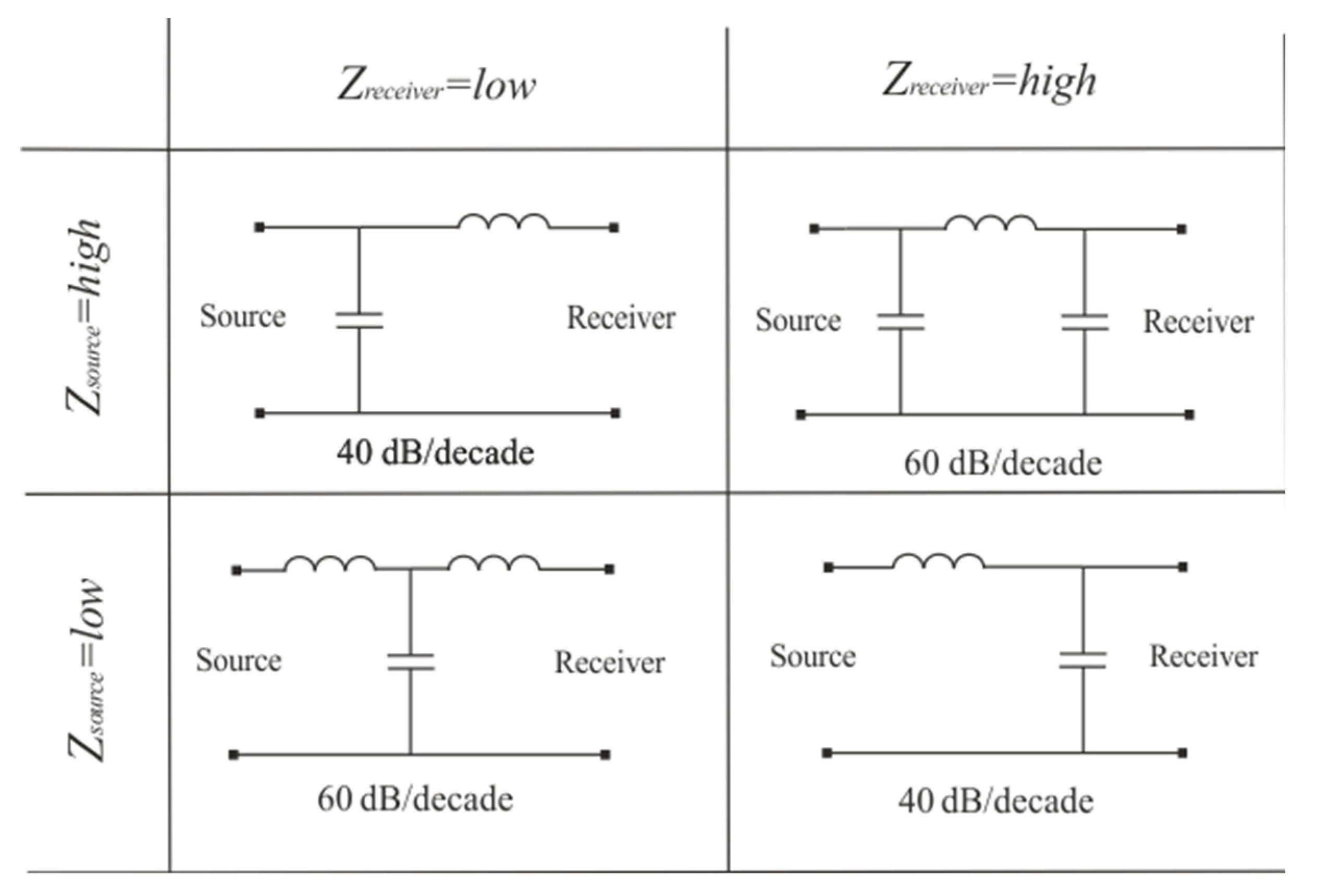
A passive discrete EMI filter (indicated in the following as EMI filter, for brevity) is composed of a CM section and a DM section, whose topologies should be suitably chosen to pursue the desired noise attenuation, but also additional requirements such as safety limits on capacitive current toward the ground, acceptable voltage drops, mismatched impedance conditions, etc. As far as the impedance mismatching is concerned, the knowledge of at least the magnitude of noise source and receiver impedances is important for the preliminary selection of the most appropriate filter topology, which is done according to the criteria shown in
Figure 1 [
7,
20], before proceeding to the filter parameter calculation. This calculation can be done in different ways. According to the conventional EMI filter design procedure, the designer considers only the intrinsic filter attenuation, which is related to the chosen topology as shown in
Figure 1, and the filter parameters are obtained starting from the desired noise attenuation at a crucial frequency (usually the attenuation required to reduce the maximum peak in the measured EMI at a level below the standard limit). This approach, even if simple and straightforward, is affected by approximation due to disregarding terminal impedances, thus considering
and
or vice versa [
26]. Therefore, this method can either lead to an oversizing of the EMI filter or non-compliance of the system with standard limits in the whole EMI frequency spectrum (150 kHz–30 MHz).
As a matter of fact, the actual trend of terminal impedances versus frequency has a significant effect on the EMI filter performance. If the EMI filter is described by its impedance matrix, as illustrated in
Figure 2, it is possible to demonstrate the dependence of the actual filter attenuation (i.e., the in-circuit IL) on noise source and receiver impedances by simply observing its expression given in (1), where the quadrupole impedance parameters appear [
27].
On such a basis, it is evident that, excluding parasitic and self-resonance effects, a more effective calculation of the filter parameters can be performed by imposing that the frequency-dependent in-circuit IL is as close as possible to the required attenuation over the whole frequency spectrum. The required attenuation, in turn, is obtained computing the difference between the EMI noise produced by the power electronic-based system and the standard limit used as a reference and considering a suitable safety margin. The filter design procedure described in
Section 4 exploits such a criterion to identify the filter parameters, reducing the possibility of oversizing or ineffective filter behavior in noise attenuation; in addition, the procedure allows finding the most suitable configuration in terms of power density as well.
3. Case Study and Filter Topology
The proposed design procedure is primarily intended for EMI filters to be used in power electronics-based applications. The chosen case study is a pulse width modulation (PWM) inverter fed induction motor drive for automotive applications, whose setup includes a field programmable gate array (FPGA) control board, equipped with a general purpose interface board (GPIB) expansion board that implements the PWM modulator.
As far as the drive control is concerned, since limited dynamic performance is requested, the induction motor is controlled using V/f control, which consists in regulating motor speed varying stator voltage and frequency at the same time. Up to the rated speed of the motor, the ratio between the stator voltage amplitude and the supply frequency is kept constant to keep the rotating magnetic flux equal to its rated value. At low speed, voltage compensation is required to avoid flux weakening due to the ohmic voltage drop on stator windings. On the other hand, above the nominal frequency, the voltage must be kept at its nominal value, so the magnetic flux decreases, thus permitting the so-called field weakening operation. The PWM frequency and the sampling frequency have been set equal to 20 kHz.
The whole V/f control algorithm, including data acquisition and PWM output generation, has been implemented on the FPGA board. This choice has been made to speed up the process by reusing a previously validated combination of development board and implemented code.
It should be noted that, in the considered case study, the required switching frequency is not high, and parallel processing is not strictly needed; thus, a microprocessor-based platform would also be a suitable choice to implement the whole V/f control algorithm. In any case, the choice of the computing platform for the control algorithm does not affect the procedure developed for EMI filter design and is out of the main focus of this paper.
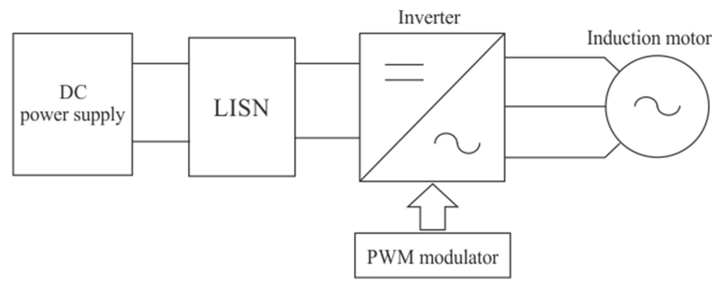
A home-built DC line impedance stabilization network (LISN) [
28] and a DC power supply are included in the experimental arrangement, as shown in the block scheme of
Figure 3.
In order to obtain the in-circuit IL of the filter, experimental characterization of the CM and DM terminal impedances in the range of frequency 150 kHz–30 MHz must be performed using a suitable LCR meter. Finally, a radio frequency (RF) clamp current probe and a spectrum analyzer are needed to measure the CM and DM EMI spectra. The main features of the experimental arrangement are reported in
Table 1, whereas
Figure 4 shows a photo of the experimental setup.
As for the selection of filter topology and its design, the LCR meter has been used to perform the experimental characterization of the CM and DM terminal impedances in the whole EMI range.
In particular, the magnitudes and phases of terminal impedances have been acquired in all the frequency range of interest, connecting the related circuits to the instrument by a suitable fixture. The tests have been managed by a Labview-based application executed on a personal computer, which is connected to the LCR meter by a IEEE-488 interface. This system allows adjusting all instrument settings, accessing the measured values, and representing them graphically. For the terminal impedances measurement, the following settings were selected: a start frequency of 100 kHz, a stop frequency of 30 MHz, and a frequency step of 100 kHz. For each performed measurement (i.e., , , , and ), a vector of complex impedance values (magnitude and phase) with a number of elements equal to the number of tested frequencies has been obtained.
Figure 5a shows the frequency characteristics of the CM noise source impedance (
) and CM noise receiver impedance (
). Likewise,
Figure 5b presents the frequency characteristics of the DM noise source impedance (
) and DM noise receiver impedance (
). As demonstrated by the experimental characterization of the terminal impedances, both the CM and DM noise source impedance magnitudes in such a case are higher than those of the noise receiver impedance (i.e., the impedance of the LISN sketched in
Figure 3) in almost all the frequency range of interest. Therefore, in principle, according to
Figure 1, it would be possible to focus the study on a Γ filter topology for both CM and DM sections, where the capacitive components are placed in parallel with the high impedance noise source (i.e., the electrical drive) and the inductive components are placed in series with the low impedance load source (i.e., the LISN) [
20]. However, it is necessary to consider the physical realizability of the filter, which depends on the availability of suitable components.
It should be noted that, whereas CM capacitor size must be limited due to safety constraints related to maximum allowable ground currents [
29,
30], in theory, the same does not apply to DM capacitors. However, with specific reference to the DM section of the EMI filter, considering the poor frequency performance of large capacitors, i.e., those much larger than 10 μF (which exhibit self-resonance phenomena at frequencies below 100 kHz), a П-configuration with two small DM capacitors is preferred to a Γ-configuration with one high-valued DM capacitor.
For the sake of simplicity, the analysis considers only single-stage CM and DM EMI filter sections, whose schemes are sketched in
Figure 6; with reference to such schemes, the CM and DM EMI filter sections impedance parameters are expressed by Equations (2) and (3), respectively [
31]. Finally, it is worth noting that a commonly used notation for filter capacitors is
Cx,
Cy; for a DC or single-phase AC system, it is
Cx = CDM and
Cy = CCM/2.
4. The Proposed Filter Design Procedure
The proposed design procedure is an improvement over the rule-based procedure described in [
25]. Therefore, the reader is referred to [
25] for the common implementation details. In the following, only the similarities and differences between the two procedures will be discussed.
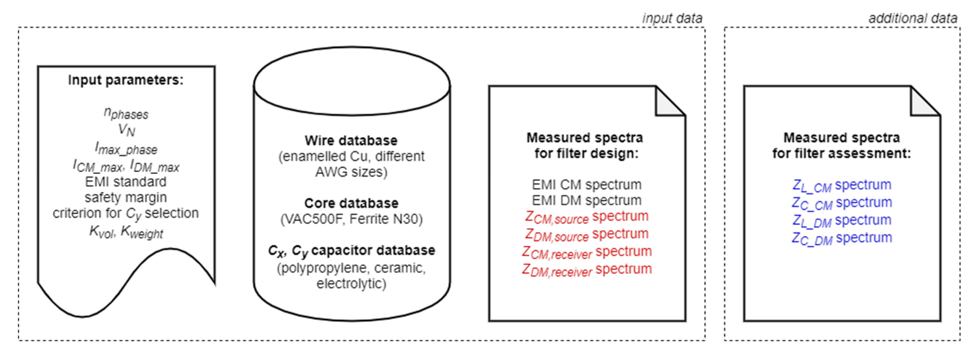
Both procedures, executed offline, take into account the characteristics of the filter application, such as the power electronic circuits and the constraints of the filter design, and exploit DBs of commercial components for the setup of the EMI filters. However, unlike [
25], the proposed procedure considers the non-ideal behavior of source and receiver in the design stage; furthermore, it performs a final assessment of filter performance to evaluate the effect of the non-ideal electrical components used. Therefore, it needs more input data and also additional validation data. The flowchart of the proposed procedure is shown in
Figure 7, and the different blocks with respect to the flowchart of [
25] are highlighted using light red and light blue colors. The input data of the proposed procedure are summarized in
Figure 8, highlighting the new required data in red. The same figure also shows the additional data needed for filter assessment, reported in blue font.
As in [
25], a prerequisite for running the filter design procedure is the knowledge of the main parameters of the system to which the filter should be connected, i.e.:
the number of AC phases (or DC lines) of the power electronic system (nphases);
the nominal voltage of the power converter (VN);
the maximum phase/line operating current (Imax_phase);
the maximum values of the CM and DM currents (ICM_max, IDM_max);
the EMI standard to which the filtered EMI should be compliant (e.g., MIL-STD-461G, EN 55011 class A, EN 55011 class B, DO160F cat. B, DO160F cat. L);
the safety margin, typically equal to 6 dB;
the criterion for Cy selection (either SAE AES 1831 standard or the maximum ground leakage current).
In addition, since the objective function to be minimized in order to increase power density is a linear combination of weight and volume, the designer must also provide the values of the related coefficients Kvol, Kweight, chosen according to the pursued goal.
Suitable DBs have been created storing the main electrical and geometrical parameters and the weight of a selection of devices available in the market. Such devices include magnetic cores (in ferrite and nanocrystalline materials), enameled copper wires to realize core windings, and capacitors with different dielectrics (ceramic, polypropylene, and electrolytic) to be used as Cx and Cy capacitors in filters for applications with power levels up to 1 kW.
Furthermore, some measured spectra are also required as input data. As in [
25], the measured spectra of the CM/DM EMI must be provided by the designer, so that they can be compared with the EMI limit mask imposed by the chosen standard over the entire EMI frequency range, also considering the safety margin. In addition, the proposed procedure requires the measured source/receiver CM/DM impedance spectra of
Figure 5, i.e.,
,
,
, and
. Therefore, such data are highlighted in red in
Figure 8.
The preliminary operations are the same for the method of [
25] and for the proposed procedure. According to the flowchart of
Figure 7, the most suitable wire size is selected from the DB on the basis of the maximum phase current; then, the maximum number of turns is computed for each core in the DB using such wire size. This operation usually leads to a first reduction of the number of feasible cores for the chosen filtering application. Next, the value of
Cy is computed according to the criterion set by the designer; then, the most suitable capacitor in terms of rated capacitance and voltage, as well as minimum volume/weight, is selected from the DB. Hence,
over the entire EMI frequency range is a known quantity.
4.1. Required CM Attenuation Profile and Computation of Theoretical Using GA
The first two light red blocks highlight the first difference with the former approach. Given the CM EMI spectrum, the chosen standard limit, and the safety margin, the algorithm presented in [
25] identifies only one crucial point among the more relevant peaks at the lowest frequencies where the CM EMI spectrum exceeds the standard limit. In this way, the required CM attenuation (
) and the related frequency (
) are obtained. Then, on the basis of the intrinsic CM filter attenuation, the algorithm computes first the corner frequency of the CM filter section, and then the theoretical common mode inductance value
that determines such frequency in conjunction with the value of
Cy.
In the proposed procedure, instead, the required CM attenuation profile over the entire EMI frequency range is computed by subtracting the EMI limit mask imposed by the chosen standard from the measured CM spectrum, including the safety margin. Then, a genetic algorithm (GA) is used to compute the theoretical value of that produces the minimum required insertion loss profile , i.e., the one that is always above and as close as possible to it.
It is worth noting that several theoretical and meta-heuristic techniques have been extensively employed in the field of power electronic and electrical drive systems to pursue optimization goals, for example in [
32,
33]. However, due to the simplicity of the problem formulation in the application under study, GAs are considered a suitable tool to solve the problem of finding out the minimum required insertion loss profile.
Genetic algorithms are meta-heuristic algorithms inspired by natural evolution and used to solve optimization problems. A population of individuals represents the set of candidate solutions, and each individual has a set of genes that encode the variables of the optimization problem. A fitness value is associated with each individual using the objective function of the optimization problem. The algorithm starts from an initial population and applies genetic operators to obtain a new population for each iteration (generation). In particular, at each iteration, a portion of the population is selected to breed a new generation; individuals with better fitness value are more likely to be selected. Then, the genetic operators of crossover and mutation are applied to the selected individuals to obtain the new population. After a fixed number of generations, the best-performing individual of the final population is selected as a solution. GAs, with respect to other optimization algorithms, present the advantage of being more robust to the presence of local maxima (or minima) in their ability to find the global maximum (or minimum) of a pre-defined fitness function.
To compute the theoretical optimal value of
, the GA randomly initializes a population of 100 elements, whose gene represents the value of
, with values in its typical range (i.e.,
), and lets it evolve through 100 generations. The choice of such an interval is not critical; in fact, through the application of genetic operators, the gene of individuals can assume values even outside this initialization range. The only constraint imposed on the gene is that it must be greater than zero. It is worth noting that the parameters of the GA were selected empirically due to the simplicity of the mathematical problem to be solved. At each generation and for each element, the value of
is used to compute
. This quantity can be used together with
to compute the quadrupole parameter values at each frequency using (2), and in turn, to obtain the corresponding frequency profile of the insertion loss
using (1). This last task also requires the knowledge of the measured spectra of
and
. The objective function to be minimized, which is evaluated for each element at every generation, is the following:
This function makes sure that the optimal
is as close as possible to
but always greater than it.
Figure 9 shows the evolution of its value for the best individual of each generation for the presented case study, and this indicates that the chosen number of generations and population size are adequate for the algorithm to converge to a solution.
After the execution of the GA, the gene of the best element of the population at the last generation represents the theoretical common mode inductance value that produces the minimum required IL profile. It should be noted that further refining of the obtained theoretical value using, for example, other metaheuristics would be futile since it is used as a starting point to select feasible components, which are discrete in the value of their parameters.
4.2. Selection of Feasible Inductor Configurations
The next step is the same for the proposed procedure and the one presented in [
25]. Once the theoretical
value has been computed, a set of feasible
configurations are produced, i.e., those for which the required number of turns is compatible with core size and does not imply core saturation. Each configuration exhibits a leakage inductance
(equal to 0.1–2% of
, depending on the core material), which will be used as the
of the DM filter section. It is worth highlighting that selecting the best
configuration at this stage would not be correct because the pursued goal is to improve the power density of the whole filter, not that of the CM and DM sections separately. Therefore, the design of the DM filter section and the computation of the DM components’ volumes/weights must be performed for every
configuration of the feasible set, so that the whole filter volume/weight can be computed subsequently.
4.3. Required DM Attenuation Profile and Computation of Theoretical Cx Using GA
Again, the other two light red blocks in
Figure 7 highlight the difference between the two approaches. Given the DM EMI spectra and the chosen standard limit, including the safety margin, the algorithm presented in [
25] identifies only one crucial point among the more relevant peaks at the lowest frequencies where the DM EMI spectrum exceeds the standard limit. Then, on the basis of the obtained DM attenuation (
) and related frequency (
) as well as the intrinsic DM filter attenuation, the algorithm computes, for each
configuration, the corner frequency of the DM filter section and then the theoretical
Cx value that determines such frequency in conjunction with the
associated to the
.
In the proposed procedure, instead, the required DM attenuation profile
over the entire EMI frequency range is computed by subtracting the EMI limit mask imposed by the chosen standard from the measured DM spectrum, including the safety margin. Then, another instance of the GA is used repeatedly to compute the theoretical differential mode capacitance value
Cx that produces the minimum required DM insertion loss profile
for each feasible
configuration. The number of elements and generations are the same as before. This time, the gene of each element is the value of
Cx (randomly initialized with values in the range
), and it is used to compute
. The profile of
is computed from the knowledge of the
associated with the
. Then,
and
are used to compute the quadrupole parameter values at each frequency using (3) and, in turn, to obtain the corresponding frequency profile of the DM insertion loss
using (1). This last task also requires the knowledge of the measured spectra of
and
. The objective function that is minimized to perform the DM design is (5) and has the same structure as (4).
4.4. Optimal Filter Configuration Selection
After the repeated execution of the GA, the theoretical
Cx value for the DM section is obtained for each feasible
/
configuration, as in the former approach [
25]. Therefore, the subsequent steps in the flowchart of
Figure 7 are the same for the two approaches. Starting from the theoretical
Cx values, suitable capacitors in terms of rated capacitance and voltage, as well as minimum volume/weight, are extracted from the DB. In this way, a set of candidate
Cx capacitors for the DM section is obtained, i.e., one for each feasible
/
configuration. Then, for each filter configuration (i.e., for the corresponding CM and DM sections), the overall volume and weight are evaluated, and the objective function to be minimized for achieving the power density goal is computed as a linear combination of such quantities using the coefficients
Kvol, Kweight provided as input data. Finally, the filter configuration corresponding to the minimum value of the objective function is selected, and the related component values are presented to the designer. This is the final step of the design procedure in the former approach [
25]. In the proposed method, instead, filter performance is assessed as the last task, as highlighted by the two light blue blocks in
Figure 7, and explained in detail in the next subsection.
4.5. Filter Performance Assessment
The filter performance assessment requires measuring the frequency response in terms of complex impedance of the commercial components (i.e.,
,
,
Cx,
Cy) that the proposed procedure selects for the best filter configuration. In this way, the non-ideal behavior of such components, due to their parasitic elements, can be properly taken into account. Such frequency responses are additional data required by the proposed procedure with respect to the algorithm of [
25], and they are highlighted in blue in
Figure 8. In order to assess the CM behavior of the designed filter, the measured profiles of
and
in the whole EMI frequency range, obtained by the Agilent/HP 4285A Precision LCR Meter, can be substituted in (2) to recompute the quadrupole CM parameters, which in turn can be substituted in (1) together with
and
to recompute the CM insertion loss
. Then, the expected CM filter performance can be obtained by subtracting
from the measured CM EMI spectrum and comparing the obtained profile with the limit mask imposed by the chosen standard. Similarly, the DM behavior of the designed filter can be assessed processing the measured profiles of
,
,
, and
(obtained by the Agilent/HP 4285 A Precision LCR Meter) using (3) and (1) to recompute the DM insertion loss
. Then,
can be subtracted from the measured DM EMI spectrum, and the obtained profile can be compared with the limit mask imposed by the chosen standard. This final assessment is a very advantageous feature of the proposed design procedure since it allows evaluating the actual filter performance before it is experimentally built and tested in the power electronic circuit.
5. Results and Discussion
The proposed procedure for filter design has been applied to the chosen case study, and the obtained results have been compared to those obtained using the approach of [
25] with the same case study. Therefore, the following two scenarios have been considered:
scenario #1: using the approach proposed in [
25];
scenario #2: using the proposed approach according to the whole flowchart of
Figure 7.
The input data for filter design that are common to both scenarios are the parameters reported in
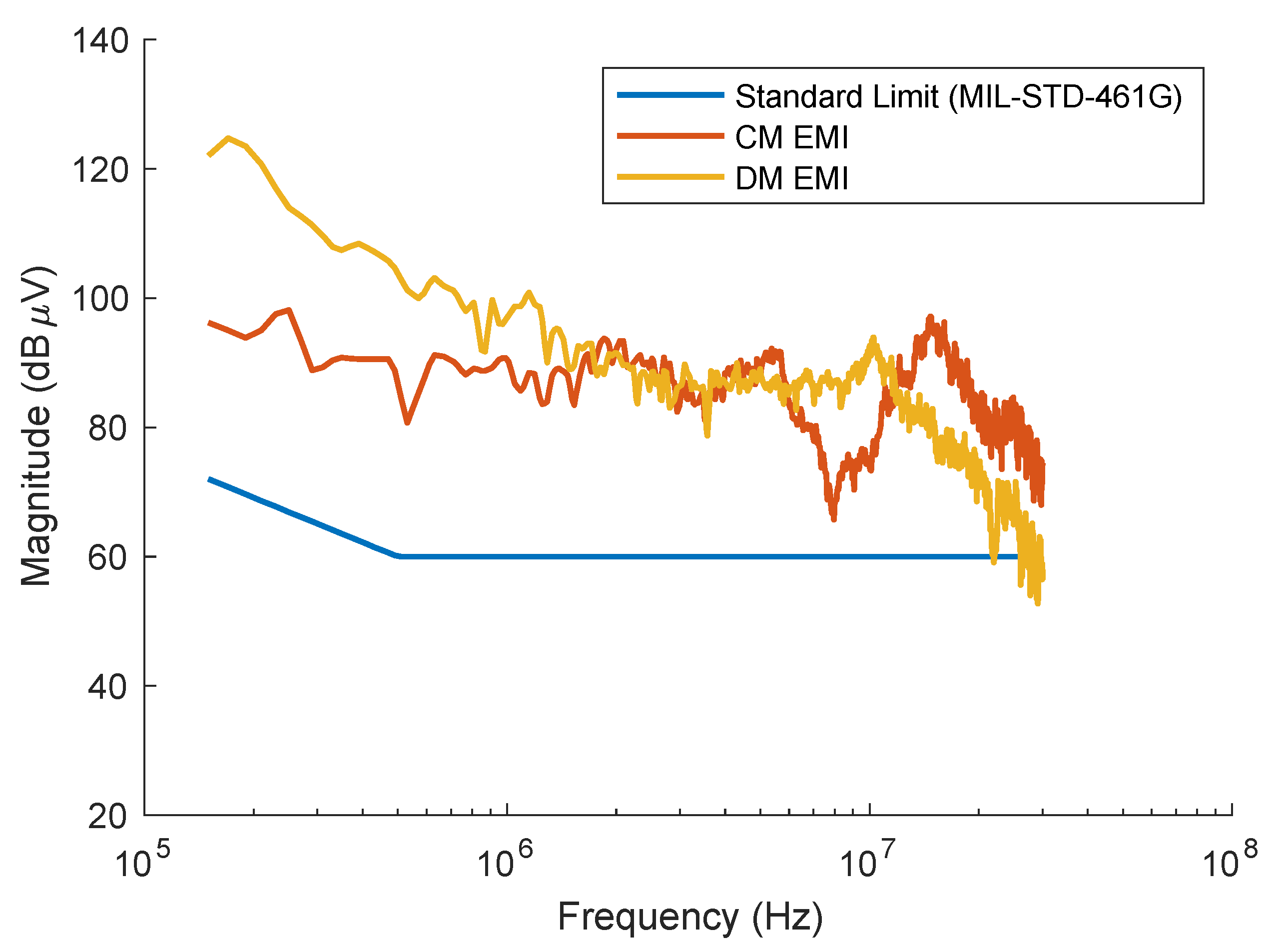
Table 2 and the measured CM and DM spectra, shown in
Figure 10. Such spectra have been measured using the RF current probe and the spectrum analyzer reported in
Table 1. The same wire, core, and capacitor DBs have been used in the three scenarios. Furthermore, the measured profiles of
,
,
, and
, shown in
Figure 5a,b, have also been used as input data in scenarios #2 according to
Figure 8.
In scenario #1, the algorithm proposed in [
25] identified the crucial points on the CM/DM spectra and determined the following attenuation requirements:
Then, it performed filter design and produced the output reported in the second column of
Table 3. The expected attenuation of the resulting filter and the expected filtered spectra are reported in
Figure 11a and
Figure 12a, respectively for the CM and DM EMI, and they show satisfying performance.
Although not included in the procedure of [
25], the filter assessment task has been performed to gain an insight into the actual performance of the filter designed in scenario #1. Following the method explained in
Section 4, the frequency response (i.e.,
,
,
, and
) of the components chosen for the filter and the CM/DM profiles of source and receiver impedances (i.e.,
ZCM,source,
ZCM,receiver,
ZDM,source, and
ZDM,receiver) have been measured. Then, the actual CM/DM insertion loss (i.e.,
and
) has been recomputed. Finally, the actual filtered CM/DM spectra have been computed. Both the actual IL and the actual filtered EMI spectrum have been plotted in
Figure 11b and
Figure 12b, for CM and DM, respectively, together with the required attenuation profile and the limit imposed by the standard. These plots show that, in this case, the designed filter will work as expected, excluding parasitic and self-resonance effects due to filter realization. In other cases, the assessment could have failed; the availability of such information even before assembling and testing the filter is crucial to the designer because it implies significant time and cost savings.
Once the need for final filter assessment has been highlighted and considering that this requires the knowledge of the CM/DM profiles of source and receiver impedances in addition to the frequency response of the filter components, it is clear that it is worth considering the former profiles in the design process, as envisaged in the proposed procedure. In scenario #2, the whole flowchart of
Figure 7 has been followed, obtaining the results shown in the third column of
Table 3; thus, these results have been obtained after the final assessment task (light blue blocks).
Although not required by the proposed procedure, the expected filter performance obtained without performing the final assessment task (i.e., without considering the actual behavior of the used inductors and capacitors) has also been evaluated for the sake of comparison. Such performance is reported in
Figure 13a and
Figure 14a for the CM and DM EMI, respectively. On the other hand, the actual filter performance (i.e., considering the non-ideal behavior of the used inductors and capacitors) is reported in
Figure 13b and
Figure 14b, together with the limit imposed by the standard, and shows satisfying performance.
The results summarized in
Table 3 show that the filter designed using the proposed procedure exhibits a significant volume/weight reduction with respect to that designed using [
25]. In particular, a volume reduction of 46% and a weight reduction of 51% are obtained.
In conclusion, the proposed procedure leads not only to an effective EMI filter, since the filtered CM/DM spectra comply with the EMI standard limits, but also to the maximization of its power density.
As for the computation time required by the algorithm of [
25] and the proposed procedure, in general, it depends on the size of the database of commercial components, which determines the number of feasible CM configurations in conjunction with the input data. However, it should be highlighted that the proposed procedure requires additional computation time with respect to that of [
25] due to the multiple executions of the GA optimization algorithm. Specifically, only one execution is required for CM design, whereas several are needed for DM design (one for each of feasible CM configuration found).
It is worth reporting that, for the considered case study, the whole calculation in scenario #1 requires, on average, three seconds, whereas each execution of the GA requires, on average, three minutes. However, these timings refer to a prototypal implementation that obviously is not developed for performance, but for accuracy. Furthermore, since the proposed algorithm is a design procedure, it is executed offline and does not have stringent time requirements.
6. Conclusions
This work proposes an enhanced automatic procedure for the design of passive discrete EMI filters, which allows considering the in-circuit insertion loss, thus obtaining more effective results with respect to these obtained considering only the intrinsic filter attenuation. At the same time, the procedure maximizes the power density of the designed filter by selecting the CM and DM inductors and capacitors to minimize the overall filter volume/weight.
Besides the databases of commercial components and the characteristics of the filter application, such as the power electronic circuits and the constraints of the filter design, the proposed procedure processes the measured spectra of the CM/DM impedance of the EMI source and receiver. Furthermore, it performs a final assessment of filter performance to evaluate the effect of the non-ideal electrical components used even before building and testing the filter; to this aim, it requires the measured frequency response of the CM and DM components selected for the designed filter. All the required measurements can be performed easily using an LCR meter capable of working in the EMI frequency range.
The design procedure relies on a genetic algorithm that is used in both the CM and DM sections to find the component values that produce the minimum required insertion loss profile, i.e., the one that is always above the required attenuation and as close as possible to it. In this way, the risk of oversizing the EMI filter or of non-compliance with standard limits in the whole EMI frequency spectrum is avoided.
The proposed procedure has been applied to a chosen case study and compared with the classic approach. The obtained results show that the obtained filter works effectively and has a higher power density than the one designed using the classic approach. Furthermore, the proposed procedure allows evaluating the real filter performance before it is practically built and tested in the power electronic circuit.

 ,
, 


