Article

Multiplexed Supply of a MISO Wireless Power Transfer System for Battery-Free Wireless Sensors

1
Chair for Measurement and Sensor Technology, Technische Universität Chemnitz, Chemnitz 09111, Germany
2
Control and Energy Management Laboratory—Electrical Engineering Department—National Engineering School of Sfax, University of Sfax, 3038 Sfax, Tunisia
*
Author to whom correspondence should be addressed.
Energies 2020, 13(5), 1244; https://doi.org/10.3390/en13051244
Submission received: 31 January 2020 / Revised: 24 February 2020 / Accepted: 4 March 2020 / Published: 7 March 2020
(This article belongs to the Special Issue Intelligent Wireless Power Transfer System and Its Application)

Abstract

:
Multi-input single output wireless power transmission (MISO-WPT) systems have decisive advantages concerning flexible receiver position in comparison to single coil systems. However, the supply of the primary side brings a large uncertainty in case of variable positions of the secondary side. In this paper, a compact multiplexed primary side electronic circuit is proposed, which includes only one signal generator, a passive peak detector, a communication module, and a compensation capacitor. The novel approach has been studied and evaluated for a MISO-WPT system having a 16 coils on primary side and one coil on secondary side having the double diameter. Results show that a standard microcontroller, in this case an STM32, is sufficient for the control of the whole system, so that the costs and the energy consumption are significantly reduced. An activation strategy has been proposed, which allows to determine the optimal transmitting coil for each position of the receiving coil and to switch it on. The time-to-start-charging at different positions of the receiving coil and different number of neighbors has been determined. It remains in all cases under 2.5 s.

Graphical Abstract

1. Introduction

Nowadays, the development of wireless sensor nodes (WSN) [1] has progressed from the implementing wake-up technologies [2] to the realization of even battery-free WSNs with low energy consumption. Battery-free based WSNs themselves can be supplied either by wireless power transfer (WPT) [3,4] or by adopting energy harvesting techniques to collect energy from one or several ambient sources [5,6,7,8]. However, energy harvesting solutions strongly depend on the availability of the ambient source in a certain environment and requires often a storage element, which help to over bridge periods of low energy availability. On the other hand, WPT systems via inductive link present a sustainable and a reliable solution to power battery-free WSNs devices, which can transfer a relative high-power level and can provide a continuous energy availability. WPT systems are generally composed of two main parts: The primary side presents the charger circuit and includes typically a signal generator, a resonant compensation capacitor, and a transmitting coil [9]. The secondary side presents the device circuit and includes the receiving coil with a resonance compensation capacitor and a rectifier to charge the device [9].
The signal generator circuit is often based on inverter circuits [10] and realizes a relatively low efficiency [11,12] because it needs to avoid overheating and therefore operates not at the exact resonance frequency. In addition, they require complex filtering stages to smooth the output voltage waveform and soft-switching topologies based on zero current switching and zero voltage switching to reach an optimized functionality [11,12]. As an alternative, AC-AC power amplifier circuits are recommended due to their pure resonance behavior [13]. In addition, WPT systems often use sensing units in the transmitting side in order to detect the presence of the receiving coil and/or control their working behavior. Various sensing units have been proposed, which can measure current [14], impedance [13], or voltage [15].
To realize a resonant behavior on both sides of the WPT system, compensation capacitors can be connected in series or in parallel to the transmitting and the receiving coils to form one of the four common topologies, which are series–series (SS), series-parallel (SP), parallel–series (PS), and parallel–parallel (PP) [16,17]. Each topology offers specific characteristics, such as the sensitivity of the load impedance variation and the intermediate air gap between transmitting and receiving coil. The single-coil WPT systems typically have a simple primary side circuit and can be therefore realized at low costs. However, the sensitivity to misalignment can be reduced by using multiple coils on the primary side. A multi-coil system allows free positioning of the receiver without increasing the energy consumption significantly only if a reduced number of transmitting coils is activated.
MISO IPT systems use several transmitting coils, which can be switched to supply receiver coil in different positions. In [18,19], authors give a review on different large area WPT systems with their coils systems, connections and supplies circuits. These systems typically present various primary side electronic architectures to power the used coil such as homogenous systems, associated single-coil WPT systems, and switch-based systems.
Table 1 presents an overview of recent and important multi-coil WPT systems architectures and their characteristics.
Homogenous multi-coil systems simultaneously activate all transmitting coils, which are connected in series to each other [25,26,27]. The used primary side supply circuit is simple and similar to the supply circuit of a single-coil WPT system. It realizes a low power efficiency and is critical for security due to the large surface of the emitted magnetic field.
To overcome these limitations, a multi-input single output wireless power transmission (MISO-WPT) system has been proposed in [23,24] consisting of several independent single WPT systems, so that after position detection only one primary side coil is activated. The magnetic field remains focused, but each single-coil WPT system needs an individual primary side supply circuit, which makes the system bulky and costly.
Switch-based MISO-WPT systems was proposed in [17,20,21,22]. Thereby switches, which are typically transistors or specific relays, are connected in series to each coil on the primary side [17], [20,21,22,23]. This reduces the size of the supply circuit relative to the previous solutions. In [19], a multi-coil system with multiplexed solution is presented with a singular supply circuit. However, the selection of the appropriate coil requires dual MOSFET switches, which presents some similarity to a switch-based multi-coil system. Nevertheless, the control of the multi-coil system switches needs microcontrollers with a high number of pins. For that, in case of a big number of transmitting coils, an FPGA [22] is proposed as processing unit, leading to an increase of both energy consumption and costs.
In this paper, we investigate the feasibility of a multiplexed circuit on the primary side supply approach, with the aim to reduce the circuit size and to control the system by a simple microcontroller with a limited number of pins. The main objective is to significantly decrease both energy consumption and system costs. To this end, we propose to use receiving coils having the double diameter of the transmitting coils. This is important to cover at least a singular transmitting coil for different possible positions on the top of the pad to power the device for all the possible positions. In order to enable the detection and the powering of even battery-free wireless sensor nodes, we propose that the communication between the transmitting and receiving coil is started from the transmitting side and supplied from the transferred energy on the secondary side.
The paper is organized as follows: In Section 2, the primary side supply circuit for a system is presented. The description of the proposed multi-coil system control algorithm is detailed in Section 3. The experimental evaluation of the developed algorithm are reported in Section 4. Section 5 shows the analysis of the required time to start the charging process. A conclusion is provided in Section 6.

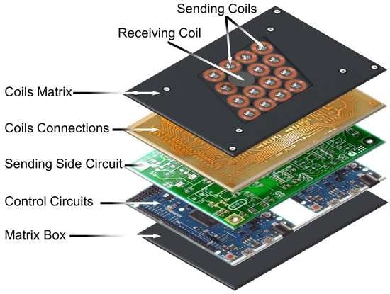
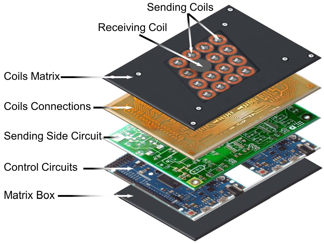
2. Design of the Primary Side Multi-Input Single Output Wireless Power Transmission (MISO-WPT) System

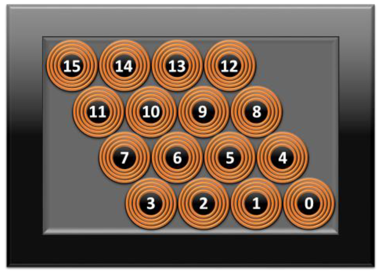
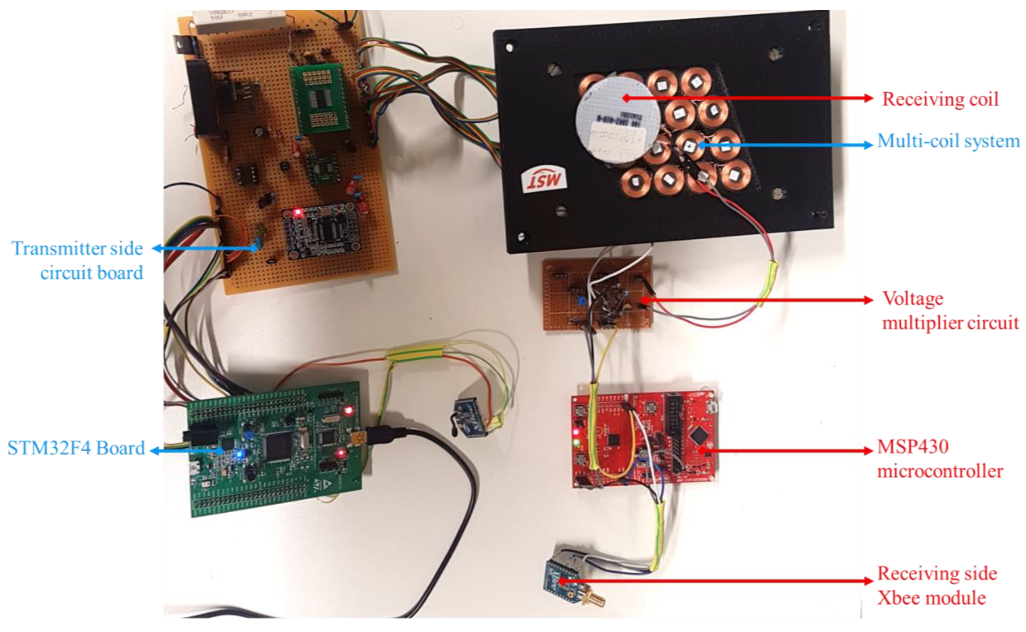
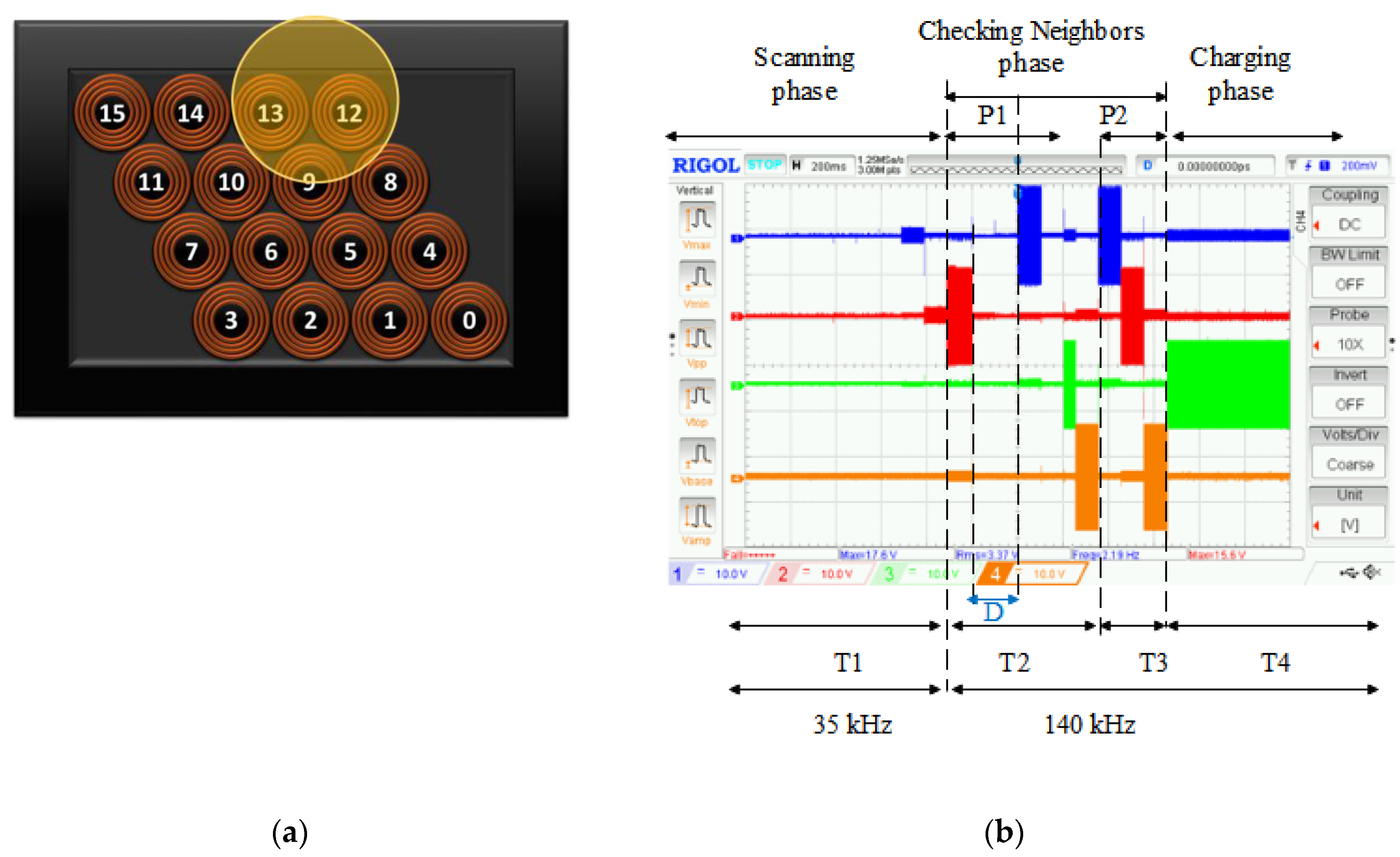
MISO-WPT systems for magnetic induction with a number of transmitting coils exceeding 10 coils present often big challenges due to the limitation on the implementation of the primary side supply circuit. One of the most challenging issues thereby is the size of the electronic circuit, which should be smaller than the size of the MISO-WPT system, especially when the transmitting coils are with a small radius. In addition, the single-layer transmitting coils arranged on multi-array configuration are critical on the activation process with the required amount of power transmission for different possible receiving coil positions within a horizontal distance of 2 mm. For that, a WPT system using 16 transmitting coils is developed with a compact size and a compact supply circuit. The coils are arranged as a parallelogram as shown in Figure 1, where the transmitting coils are indexed from the coil number 0 (C0) to coil number 15 (C15). The selected geometry is based on previous study in [26], which compares different configurations. The selected configuration offers a small airgap between the transmitter coils, which increases the transmission efficiency [26] specifically when the receiving coil diameter is double that of the transmitting one.
The working principle of the proposed multiplexed supply primary side circuit consists of the activation of transmitting coils one by one. In each coil, the system estimates the presence or the absence of the receiving devices on the top of it. Therefore, a singular supply circuit is used to reduce both circuit size and cost. Typically, using the proposed activation strategy, the system behaves as coil to coil WPT system with a singular transmitting coil and a singular receiving coil. However, the single-coil WPT system is based on the communication between the primary and the secondary sides. For that, generally, a small amount of energy on the secondary side enables the communication between both sides, which is not possible in the case of charging battery-free devices. To address this issue, an additional detector circuit is connected to the primary circuit and a continuous activated primary circuit is required. To reduce the permanently activated circuit that increases the system current consumption, a variation of the working frequency in a large range is highly needed. This solution is complicated in the case of inverter-based supply circuits. To this end, an AC-AC converter is selected as a supply circuit for the proposed multi-coil WPT system.
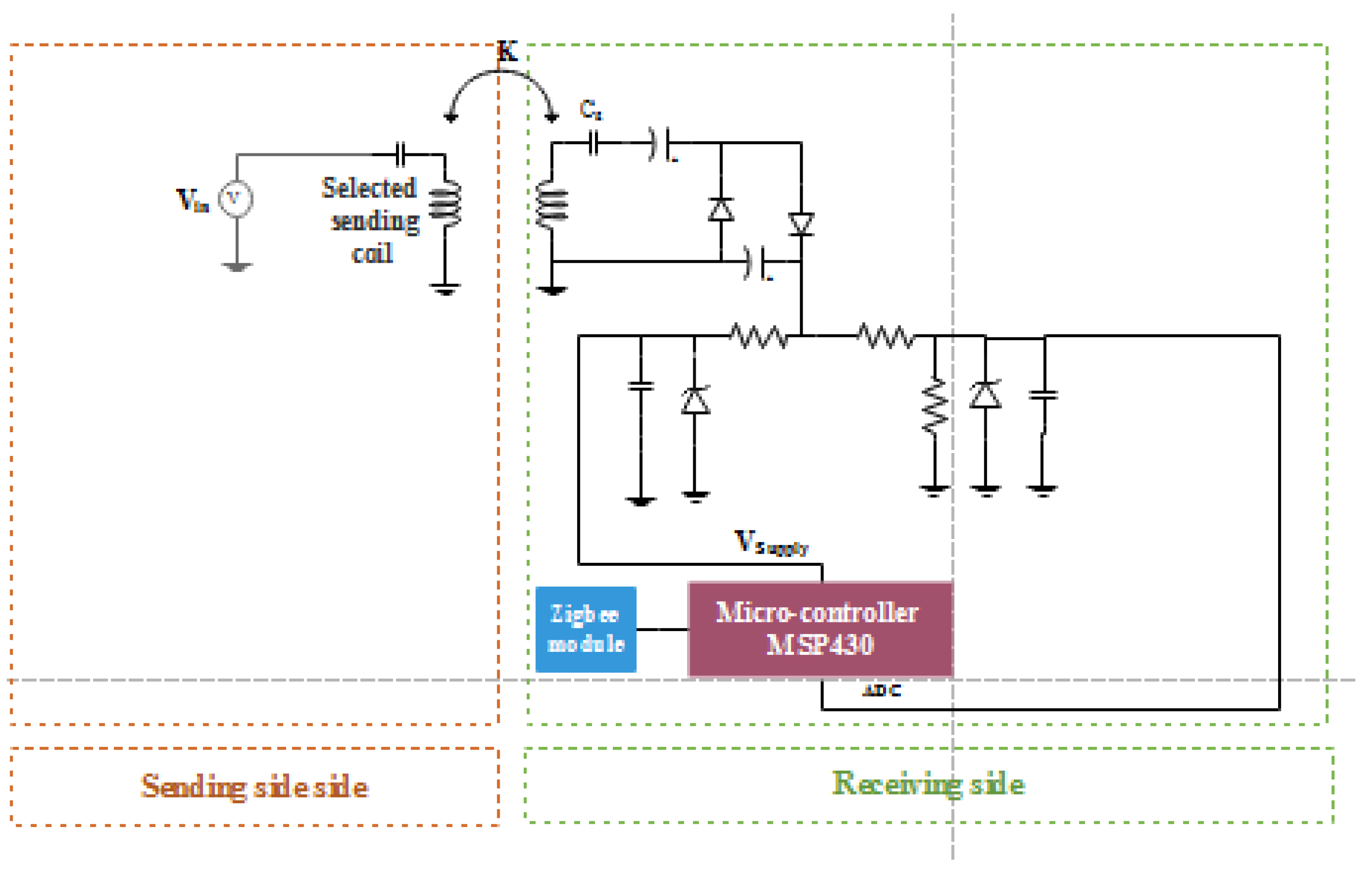
Figure 2 illustrates the proposed primary side electronic circuit. It is based on a single oscillator, a voltage amplifier circuit, a current feedback amplifier, a compensation capacitor, multiplexers, a passive voltage peak detector, a ZigBee communication module, and a microcontroller board. Indeed, multiplexers are used to switch-on the appropriate transmitting coil.
The passive peak detector circuit is used in the primary side to detect the presence of the receiver device even without communication with the secondary side. Their working principle is based on the detection of the reflected power [26] (see Equation (1)) due to the presence of the receiver coil (L2) behind it, which can vary the selected transmitting coil voltage (VL1c) [17] as presented in Equation (2). In Equation (2), the select coil self-inductance is L1 where the transmitting coil voltage and current are Vs and Is, respectively. Ceq2 presents the series compensation capacitor in the receiving side. Therefore, the proposed primary side circuit is a low power consumption device since it uses passive components including simple diode, smoothing capacitor (C) and resistors (Rsmooth) (see Figure 2). To select the values of the smoothing capacitor and the associated resistor, Equations (3) and (4) are used.
In the following analytical equations (Equations (1)–(4)) are presented in order to describe the passive peak detector principle.
Z r = ( ω M ) 2 Z 2 ,   where   Z 2 = j ω L 2 + 1 j ω C e q 2 + R L
  V S =   L 1 d i r d t + M d i 2 d t
C = I s 2 R f V L 1 c
R s m o t h > τ 5 C   ,   where   τ = R s m o o t h C
As seen in Figure 2, the detector is connected to the compensation capacitor output and the common pin of the multiplexers to measure the selected transmitting coil voltage variation.
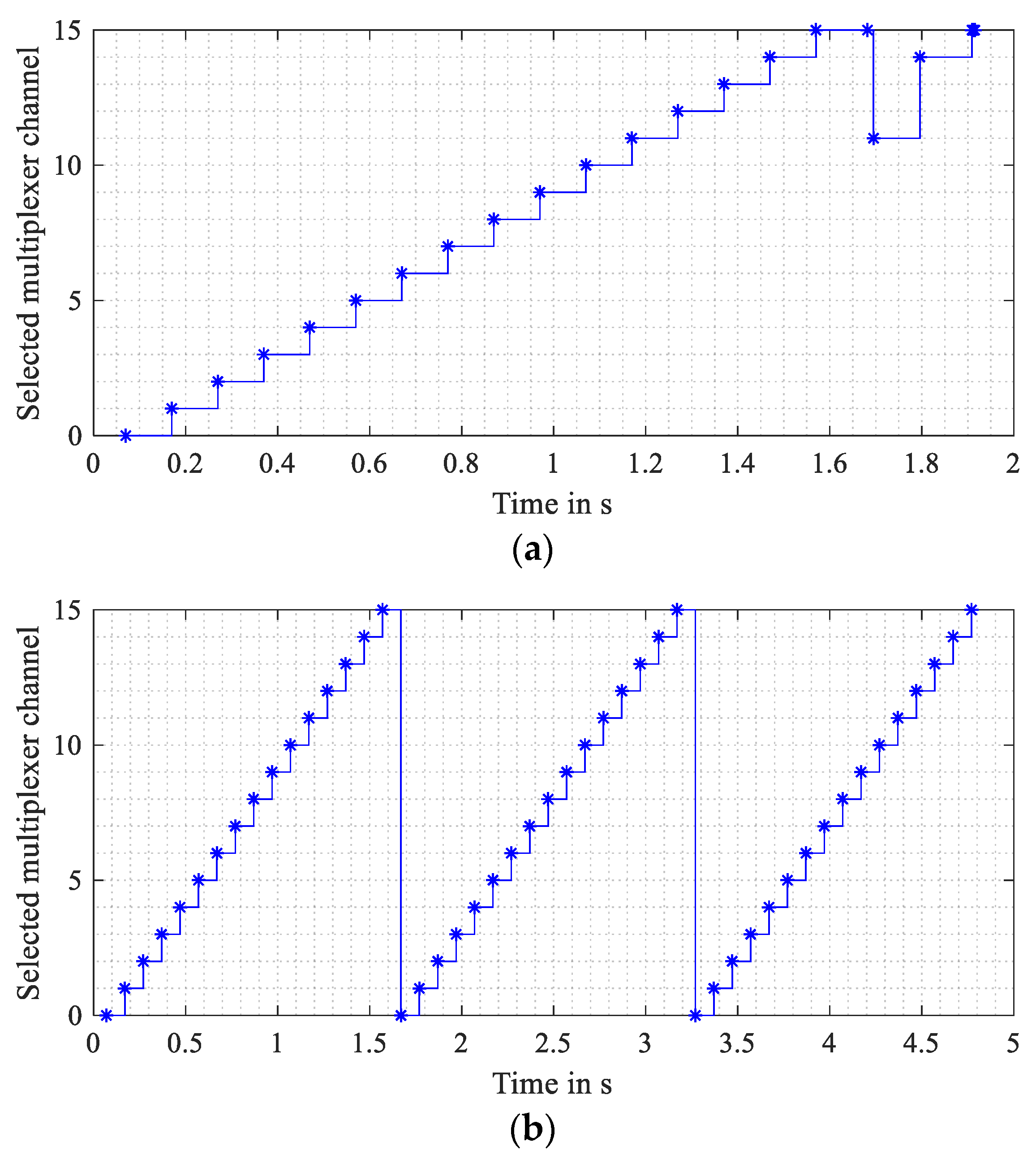
The selection of the multiplexer is critical due to the required high frequency of switching, and the used AC signals amplitude and current. An ADG1406 multiplexer with 1:16 channels characterized by a high switching frequency, a supply voltage of ±15 V, high switching frequency and a continuous current up to 180 mA is used. For that, to support the coil current, parallel multiplexers are used. The singular multiplexer channel is connected to the output pin of the primary side compensation capacitor, where the other channels are connected each to the transmitting coil. The activation and deactivation of transmitting coils are based on the five multiplexer control pins (A0, A1, A2, A3, and A4). The switch-on of a transmitting coil depends on a specific functionality combination of the multiplexer control pins as presented in Table 2. In the implementation, the control pins of both parallel multiplexers are connected in parallel, which reduces the number of the used micro-controller pins.
The proposed AC-AC amplifier is based on an oscillator connected to amplifier stages. For that, a direct digital synthesizer (DDS) generates a voltage amplitude Vin = 1 Vpp with an offset of 0.5 V is implemented. A high pass filter (capacitor and resistor) is connected to the DDS output to remove the signal offset. To increase the obtained power, a voltage and current amplifier are used to supply the MISO-WPT with appropriate voltage and current levels.
The voltage amplifier circuit is based on an AD817 op-amp to provide an adequate voltage amplitude (V2) to be doubled amplified (Vs) by the current feedback amplifier (LT1210). Both amplifiers are connected to a non-inverter architecture (see Figure 2), where the output voltages for each stage are presented, respectively, in Equations (5) and (6). The current amplifier voltage output (Vs) according to the DDS voltage (Vin) is presented in Equation (7). In the output of the current feedback amplifier, a resistance (R), a compensation capacitor (Ceq1), and the selected transmitting coil (L1c) are connected in series. The resonance compensation capacitors on the resonant frequency of 140 kHz of both sides are obtained based on Equation (8). The current (Is) generated by the proposed supply circuit depends on the generated voltage level and the connected load value as shown in Equation (9), which is maximal in the case of pure resonance. In the following analytical equations (Equations (5)–(9)) are presented in order to describe the amplifier circuit design principle and the generated supply current.
V s = ( 1 + R 2 R 1 ) V 2 = A o u t V 2
V 2 = ( 1 + R c R f ) V i n = A c V i n
V s = ( 1 + R c R f ) ( 1 + R 2 R 1 ) V i n = ( 1 + R c R f ) A o u t V i n
ω = 1 L 1 c . C e q 1 = 1 L 2 c . C e q 2   ,   where   L 1 c = L 1 M   and   L 2 c = L 2 M
I s = V o u t R + j ω L 1 + 1 j ω C e q 1 + Z r
The developed circuit gives more freedom on smooth frequency variation on a large range from a few kHz to several MHz. In addition, the pure sine wave voltage and current are generated by the AC-AC amplification stage. These advantages are challenging in case of a supply circuit based on DC-AC inverters.
In fact, the proposed circuit offers several advantages especially in term of size and cost. To design 16 MISO-WPT system with homogenous architectures, a supply circuit delivering 16 times voltage than single-coil WPT system is required, which increases the system power consumption and reduces efficiency. However, in case of for switch-based multi-coil WPT, generally 32 MOSFET switches or 16 relays are required to activate the valid transmitter coil. In addition, at least, 16 microcontroller pins are used. In the proposed circuit, only two switches chips controlled by only 5 microcontroller pins are connected to supply circuit of the 16 multi-coil WPT. In addition, commercial coils with ferrite shield are used, which offers high quality factors and standardized performance.

3. Control Algorithm for Low Current Consumption

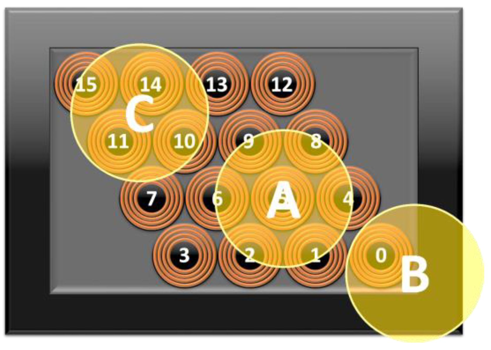
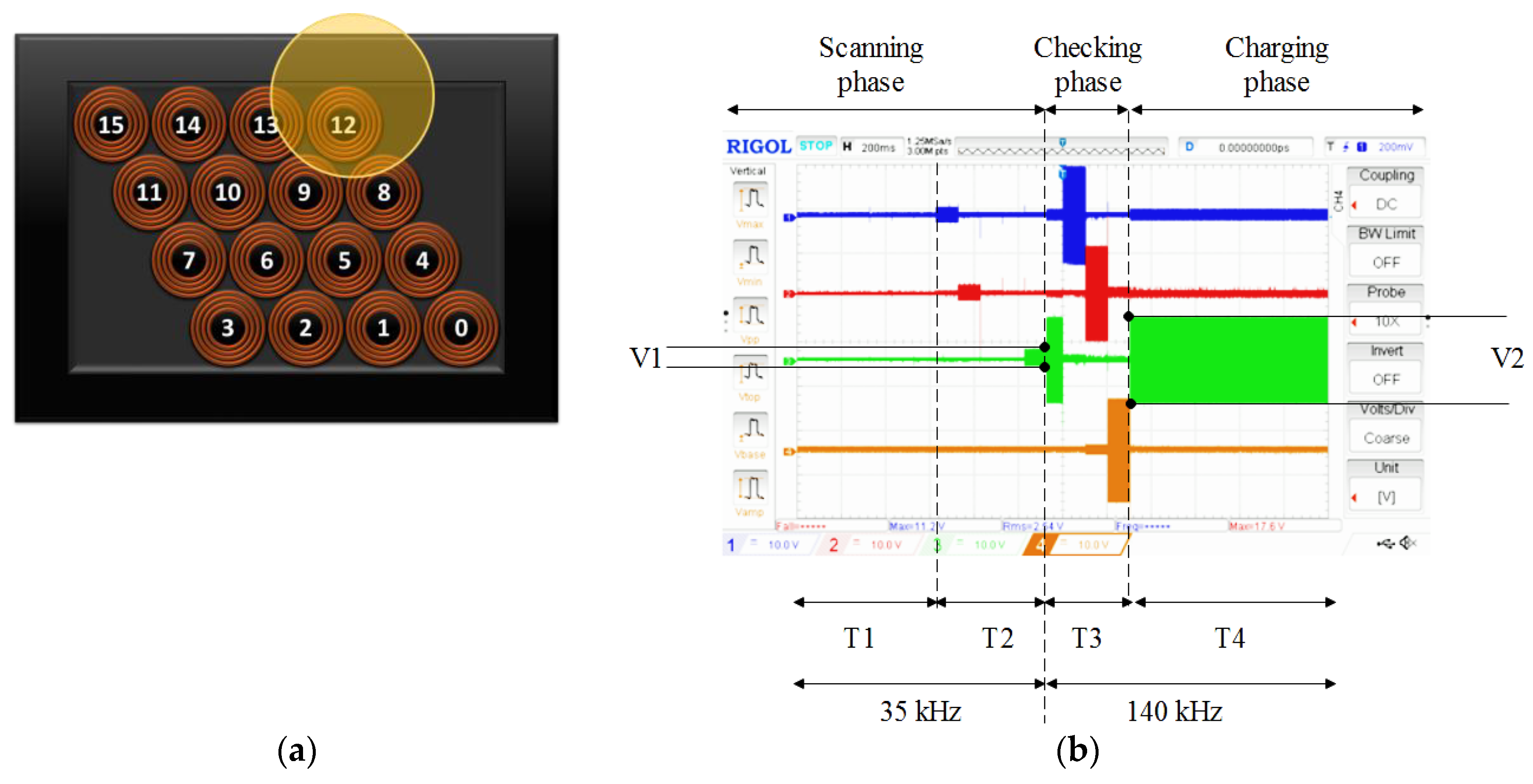
The developed MISO-WPT system allows the supply of battery-less devices for different positions with a small primary side electronic circuit. For that, the receiving coil radius is two times bigger than the transmitting coil radius, which can occupy an area of three transmitting coils. In this case, some critical charging cases can be designed. Some examples of the receiving coil positions can be defined in Figure 3 as position A (PA), position B (PB), and position C (PC). The position PA defines the ideal position between the transmitting coil (C5) and the receiving coil centers. In this case, the transmission efficiency is maximal. The PC illustrates a lateral misalignment between the receiving coil and the transmitting coil C11. While the PB presents an extremely misalignment in case of the transmitting coils on the borders of the MISO-WPT system. In the case where the receiver device is in the PC, the activated transmitting coil is selected by the comparison of the received voltage on the device. However, in the case of the PB, the powering of the device depends only on the transmitting coil placed under it. Furthermore, due to the various possible receiver positions, the detection of the adequate transmitting coil requires communication between both system sides to define the transmitting coil delivering the highest receiving voltage. By the use of the multiplexed supply circuit, the detection phase starts with identifying the presence of the receiver, then checking the selected coil neighbors to define the highest received voltage. The circuit is maintained active to detect the receiving coil, which increases the circuit current consumption during the detection phase.
A passive peak detector is associated with the circuit allowing the detection of the receiving side without communication for a low working frequency. If a voltage variation is detected, the working frequency increases to the resonance frequency, which allows the communication between both sides to check the selected coil neighbors. However, the system frequency influences not only the circuit current consumption, but also the passive peak detector circuit sensitivity.
In this section, a study of the detection frequency allowing low current consumption and good detection sensitivity is presented. Then, the developed algorithm is described in detail.

3.1. Investigation of the Working Frequency Influences on Current Consumption

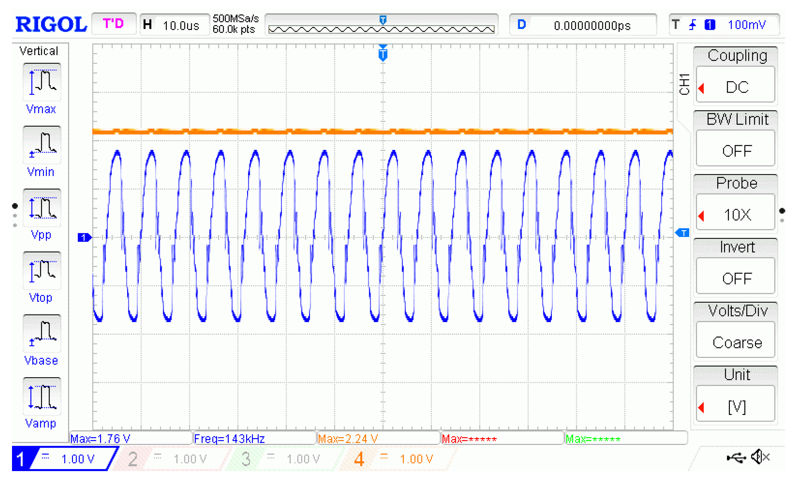
The system frequency influences the transmission efficiency, the system current consumption and the sensitivity of the passive-peak voltage sensor. 
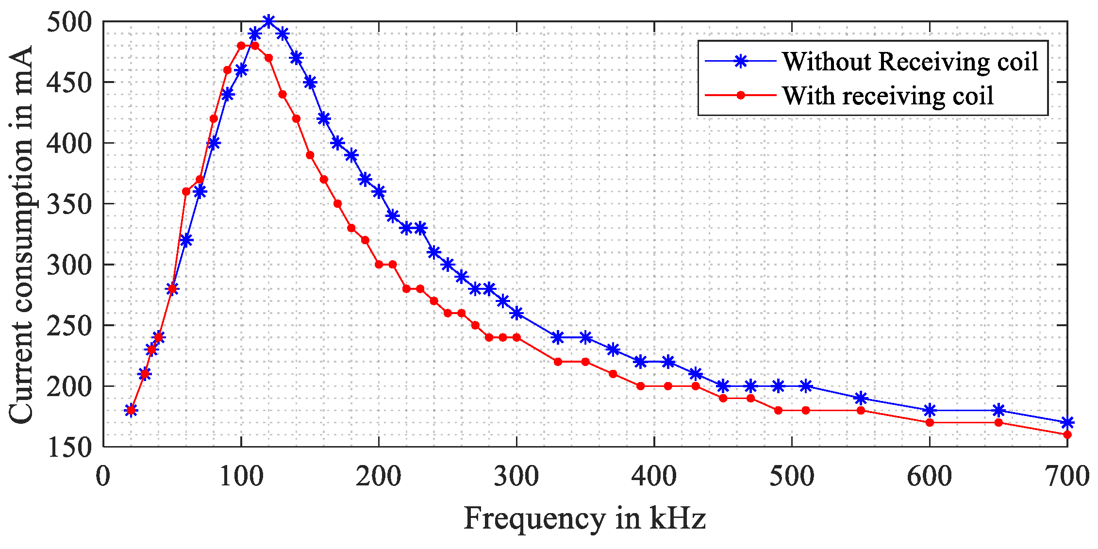
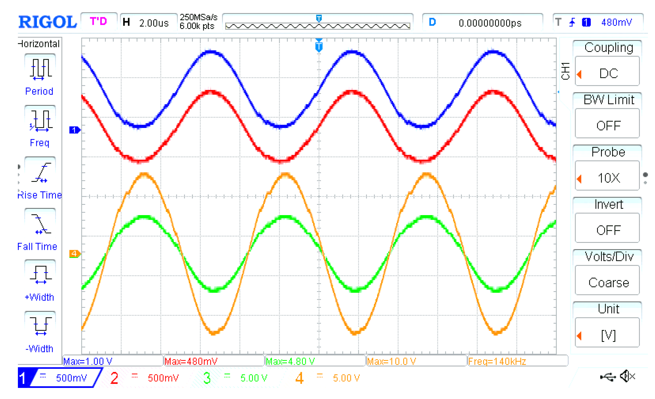
Figure 4 illustrates the circuit current consumption in case of the presence and the absence of the used WSN for frequencies between 20 kHz to 700 kHz. Results show that the current consumption increases approximately 450 mA near the system resonance frequency. However, the current consumption is less than 250 mA for the frequencies between 20 kHz to 60 kHz and above 200 kHz.
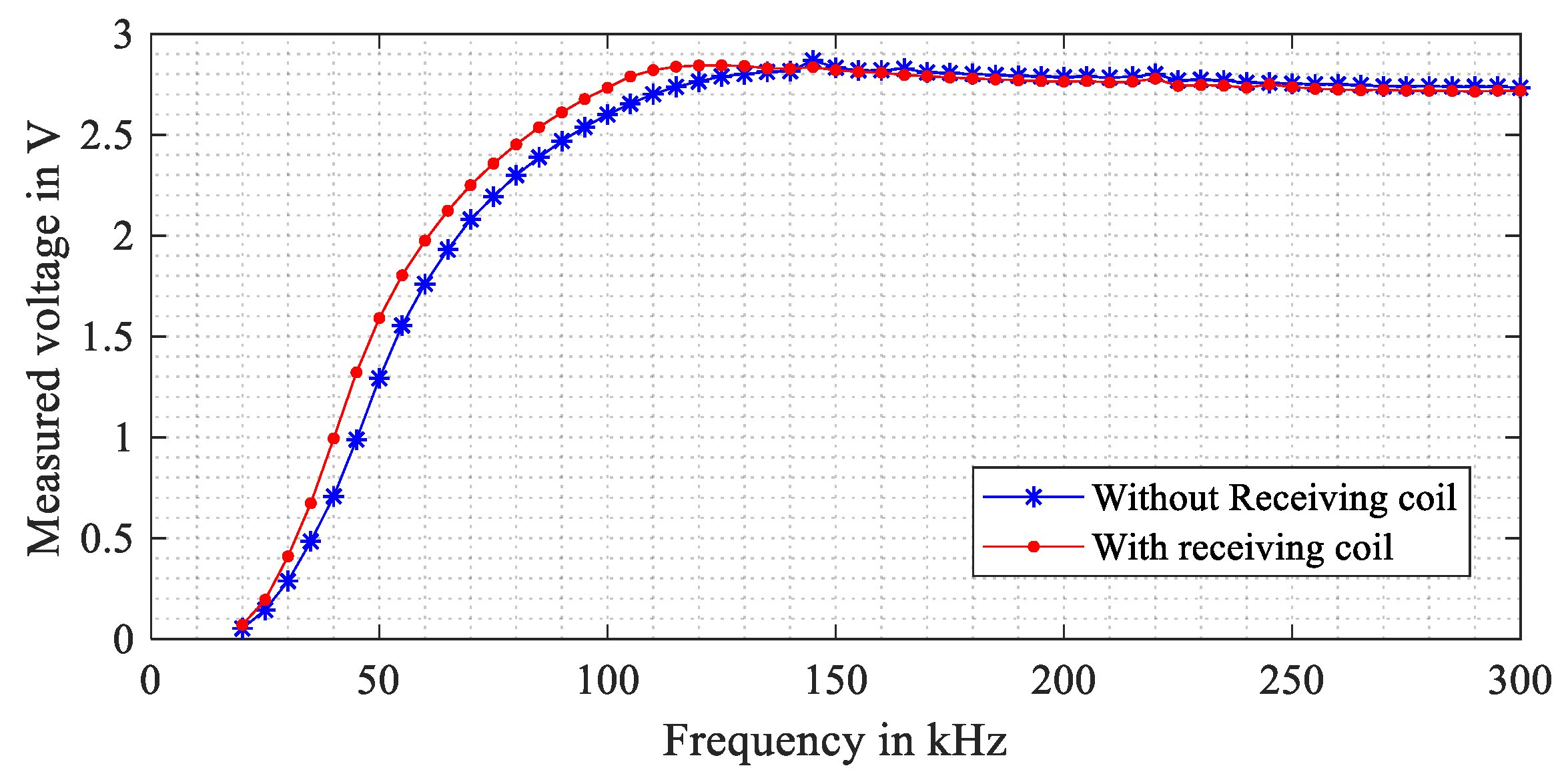
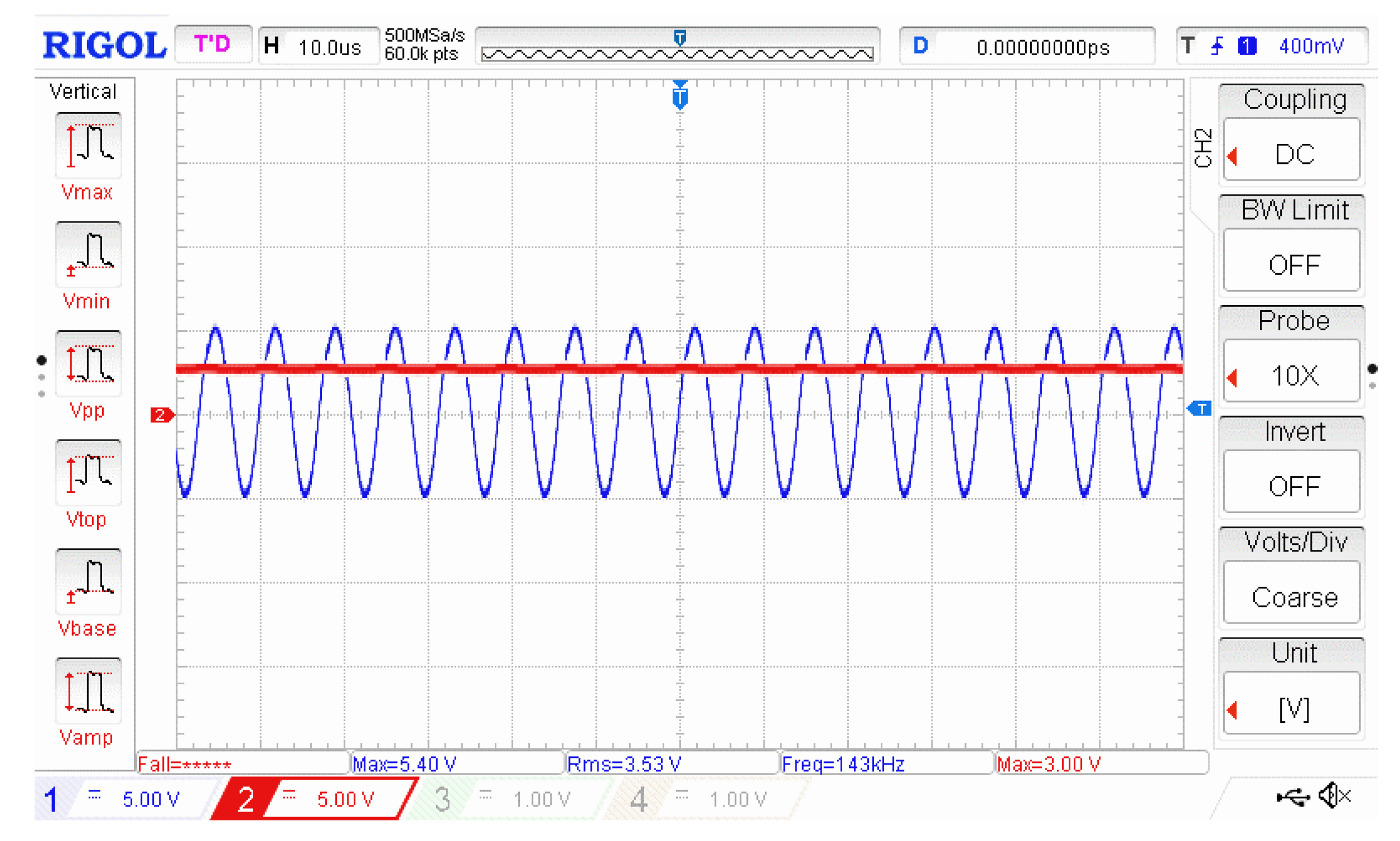
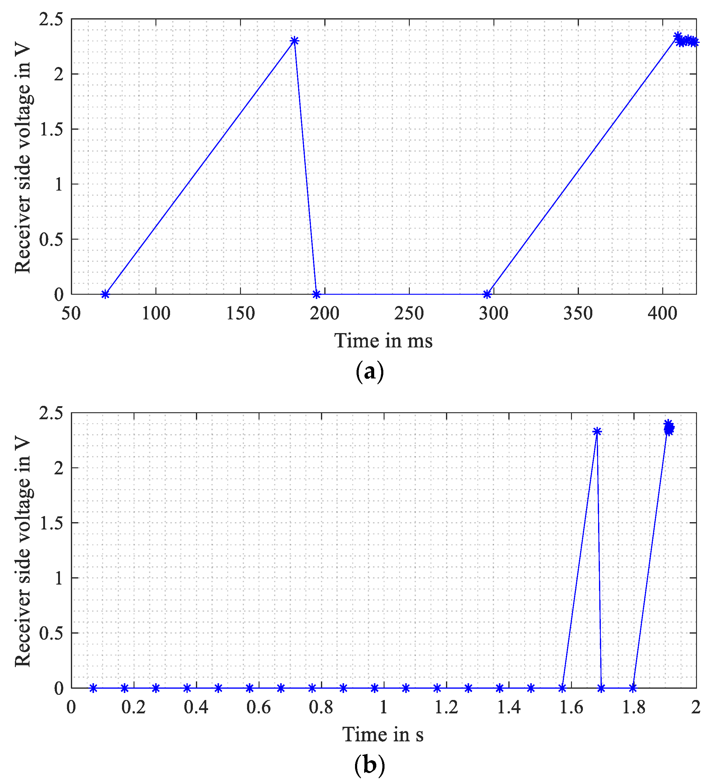
Moreover, to study the sensitivity of the receiving device detection in different working frequencies, a measurement of the peak detector voltages behavior in case of the presence (VRecei) and the absence (VNO-Recei) of the wireless sensor node on the top of an adequate transmitting coil is presented in Figure 5. In fact, Figure 5 shows among others that at 20 kHz the detectability is weak as the reflected field becomes very low. In the circuit design, an additional voltage divider and Zener diode to protect the microcontroller board are associated with the output of the passive peak sensor. Results of Figure 5 shows that the variation of the measured voltage in the case of presence and absence of the receiving coil increases near the resonance frequency.
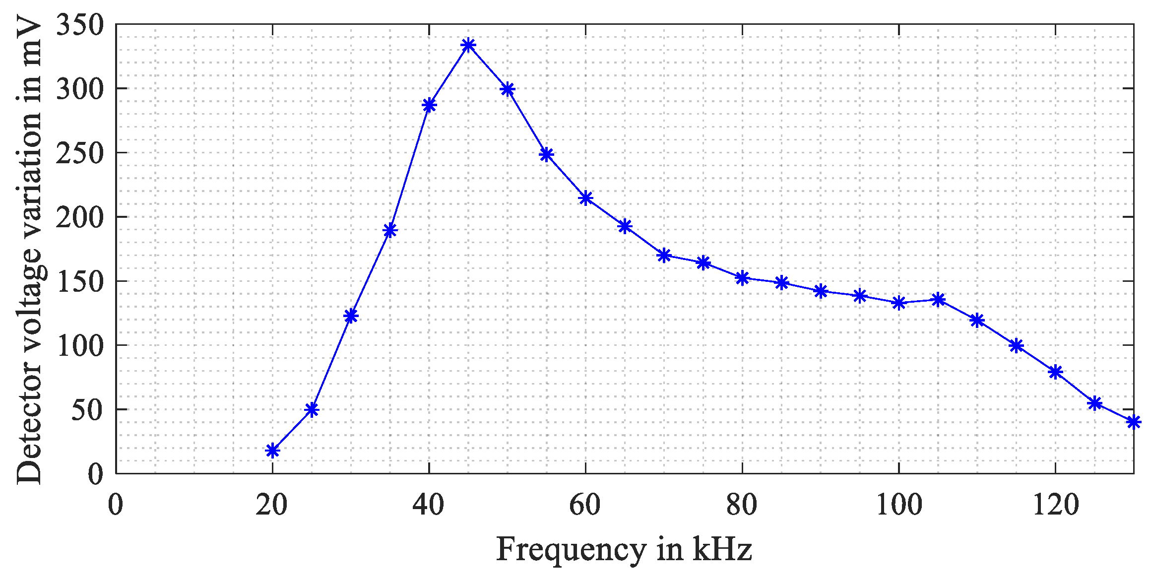
A measurement of the voltage peak detector sensitivity (ΔVdetec), which is defined as the resulting value from the difference measured voltages in the case of presence and absence of the receiving side (see Equation (10)).
Δ V d e t e c =   | V N O _ R e c e i V R e c e i |
Figure 6 shows that for a frequency between 30 kHz to 130 kHz, the detection of the presence of the receiving device is acceptable due a voltage variation more than 50 mV. For a voltage variation below 50 mV, errors during detection with a passive peak detector circuit are more common. However, for a working frequency between 35 kHz to 45 kHz, an appropriate balance between the directivity of the receiving coil and current consumption is confirmed with a low frequency reducing the possible eddy currents losses.

3.2. Proposed Algorithm

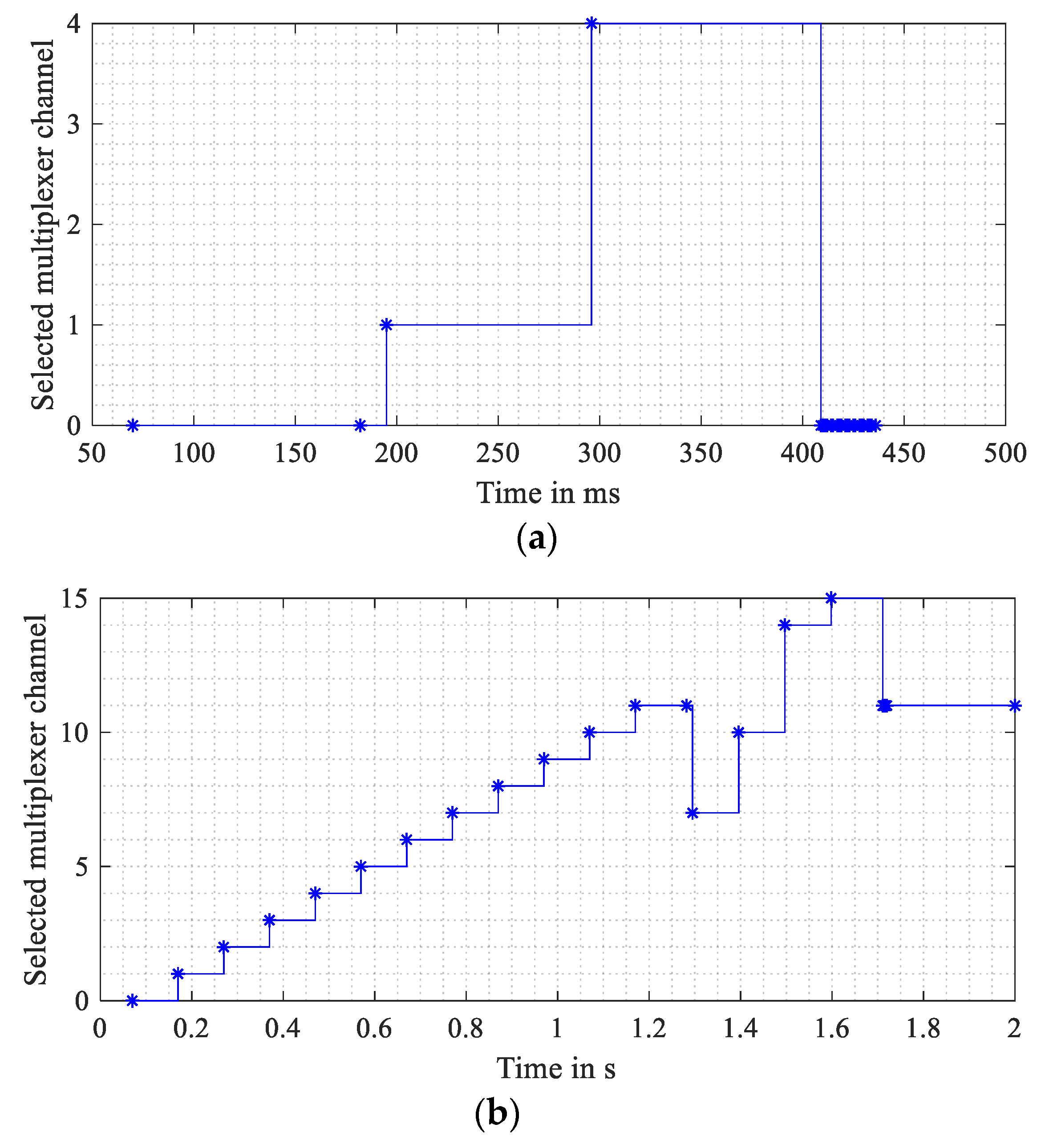
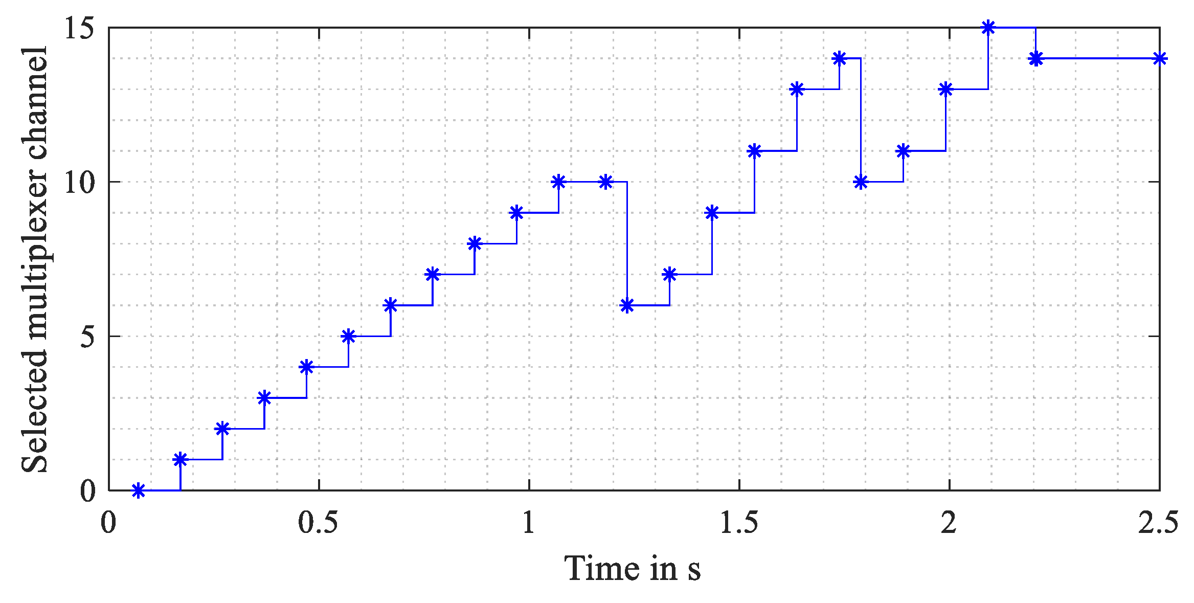
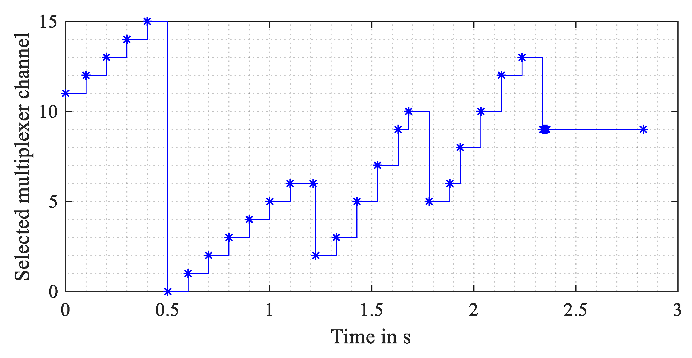
The proposed algorithm ensures the detection and the powering of the battery-free WSN on the top of the MISO-WPT WPT. Before the implementation of the algorithm, a calibration process is required to define the voltages sensor in the case of the presence or absence of the receiving side on the top of the transmitter phase.
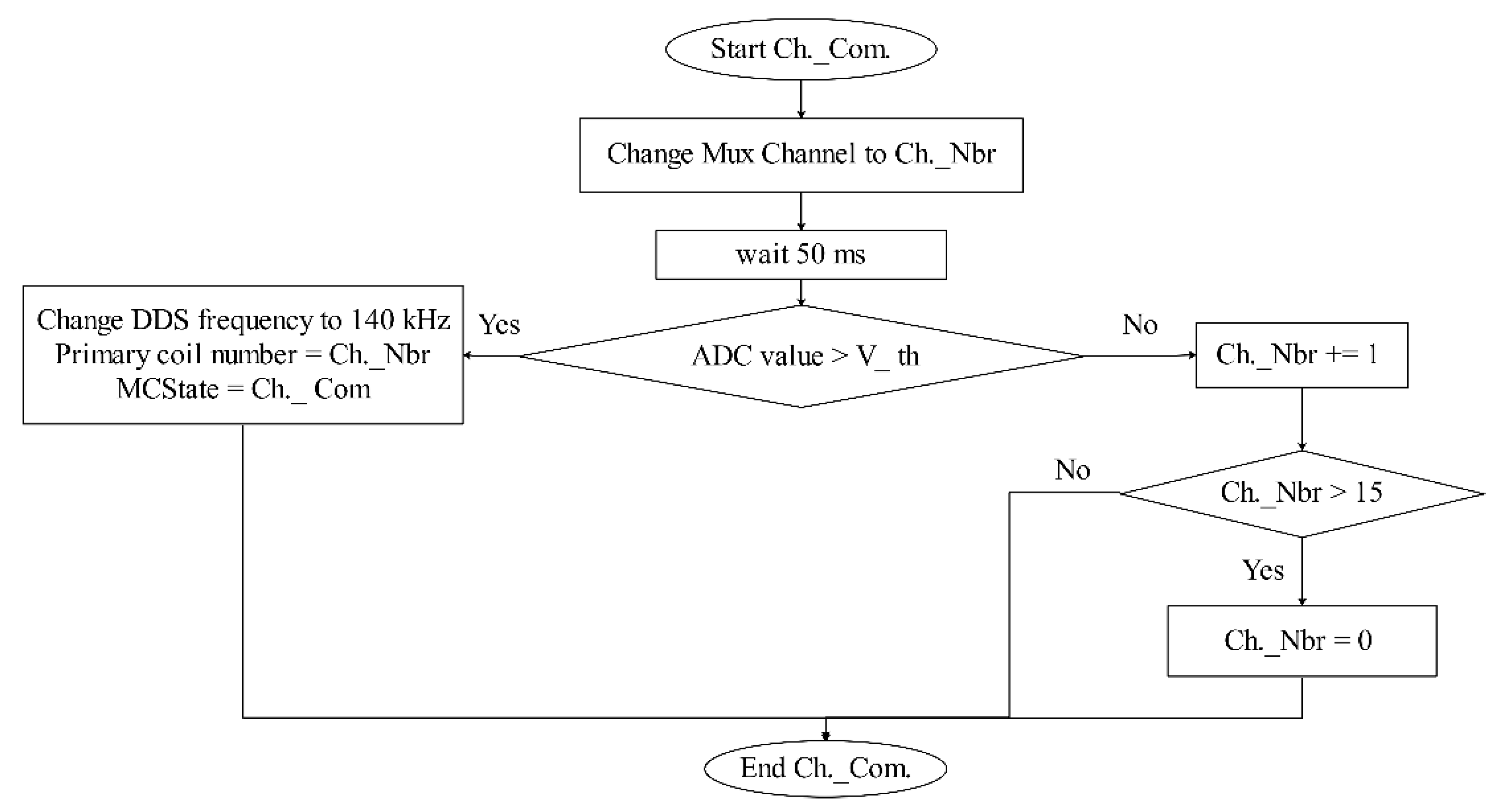
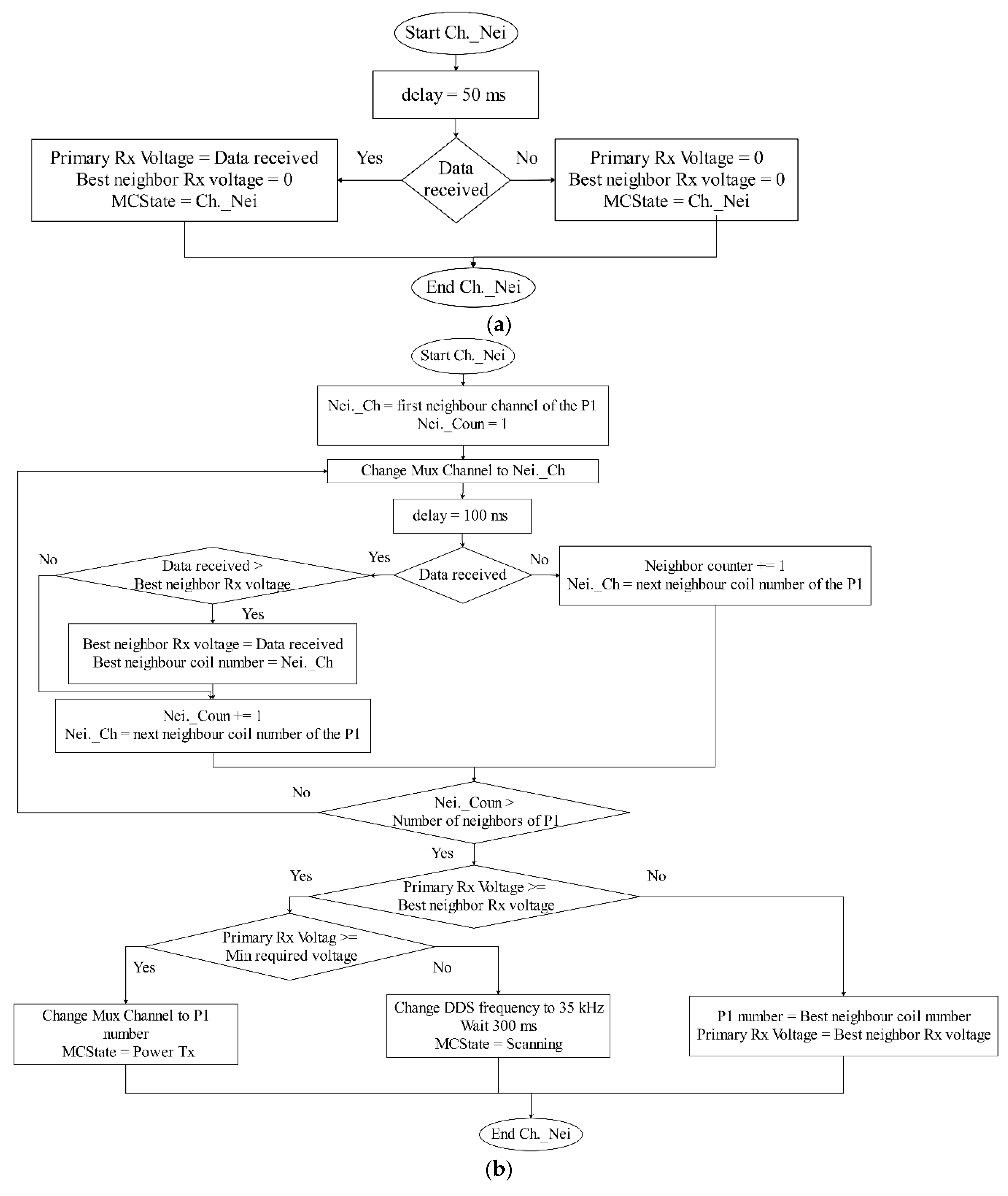
Figure 7 illustrates the main algorithm flowchart, which is composed of four sub-algorithms: Scanning phase, check the communication between coils, check neighbors, and powering transmitting coil (Tx) phase. The initialization sets the microcontroller registers, adjusts the DDS frequency to 35 kHz and ensures the selection of the first transmitter coil. The Ch._Com and Ch._Neigh refer to the check communication phase and check coils neighbors state, respectively. V_Th is the define threshold voltage and Nei.Coun. is the neighbor counter parameter. The neighbor channel is mentioned as Nei_Ch.
The scanning phase sub-algorithm presented in Figure 8 consists of the activation of the transmitting coil one by one. For each activated transmitting coil, a measurement of the peak voltage indicates the presence or the absence of a receiving device near it. If the receiving coil is detected, the system changes its working frequency to 140 kHz to increase the transmitted power and passes to the checking neighbor phase.
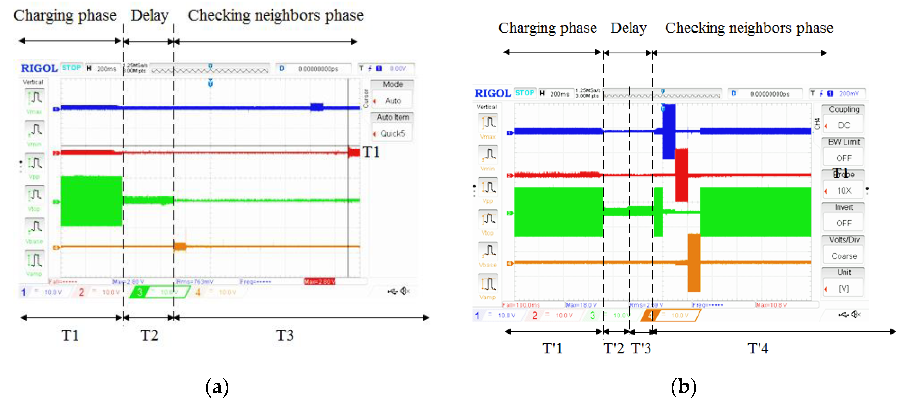
At the resonance frequency (140 kHz), the transmitted energy allows the communication between the primary and the secondary sides, which starts the check neighbor state (Figure 9a). As presented in Figure 9a, after a delay of 50 ms, the system starts to check for initiated communication from the secondary side allowing a maximum of 50 ms as a communication establishment time out. After the time out, if a communication between the transmitter and the secondary side is not detected, the system continues the scanning phase by moving the next transmitter coil; otherwise, the check-neighbor phase is activated. It consists of activating neighbors one by one and checking, for each one, the existence of communication with the receiver coil (see Figure 9b). The selection of the adequate transmitting coil to start the powering process refers to the index of the coil with the maximum received voltage level considering both the primary coil and its neighbors. The primary coil is selected for power transmission if it has a higher received voltage than its neighbors. In the case of the existence of neighbors with higher received voltages than the primary coil, the neighbors of the neighbor coil with the maximum received voltage are checked in the next iteration. If the communication between the transmitter and the secondary sides is not established, the system returns to the scanning phase.
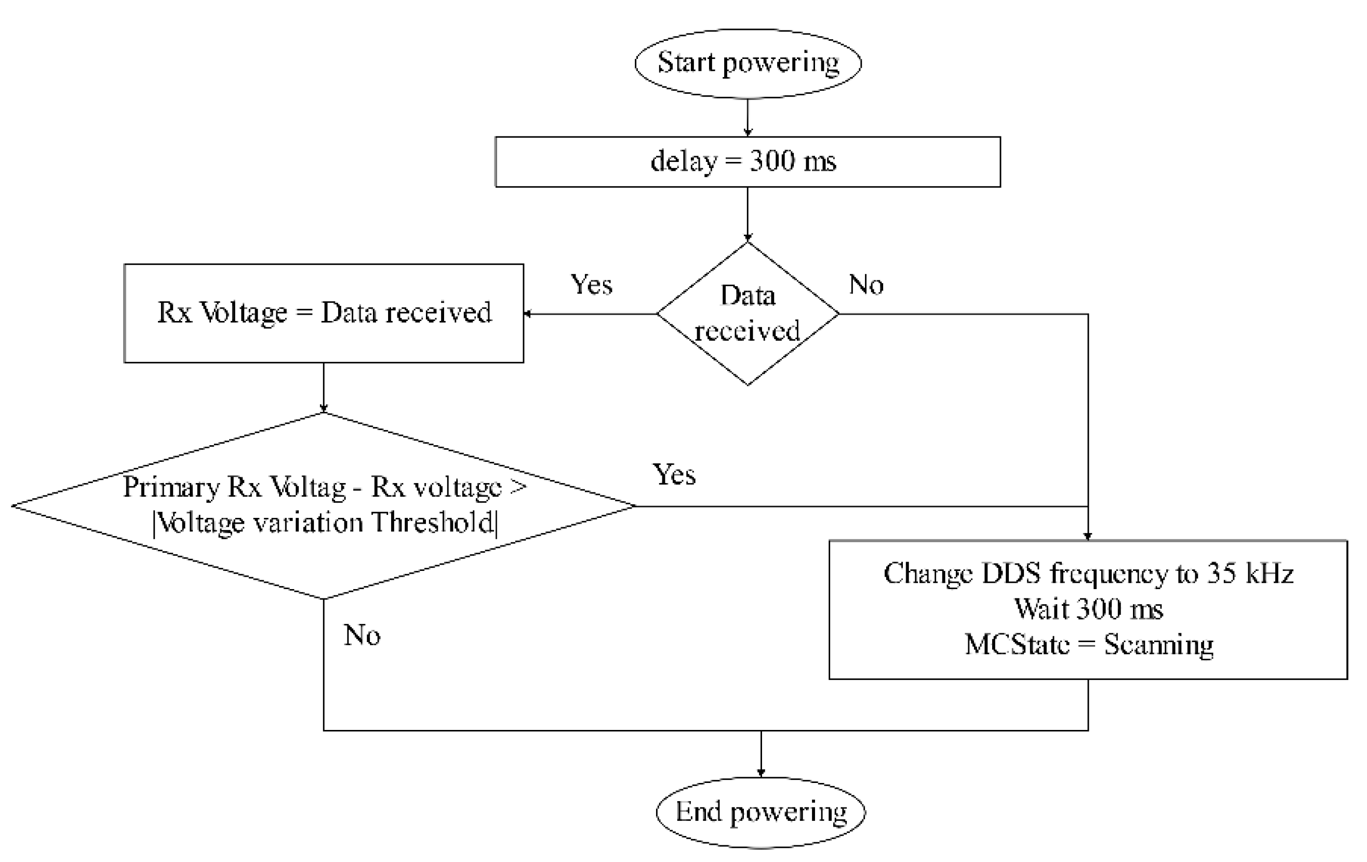
During the powering phase (see Figure 10), a continuous communication between the transmitter and the secondary sides is maintained to ensure the developed system security. If the communication is stopped due to the absence of the WSN or a variation in the received voltage is detected with a magnitude higher than a predefined threshold, the system switches to the scanning phase and switches to an operation frequency at 35 kHz.

4. Experimental Evaluation

The experimental validation of different WPT systems can be processed with different methods such as the measurement of the generated magnetic field in different positions based on FEM simulations [27] and the measurement of the system efficiency and the obtained load power [20]. Others present the implemented algorithm in different conditions [28], which is more appropriate to prove the feasibility of the proposed circuit. In this paper, the focus is on the implementation of the MISO-WPT control algorithm for a multiplexed supply circuit.

4.1. Hardware Description

The used battery-free WSN requires a threshold voltage of about 2 V and includes an MSP430 board connected to the ZigBee module to communicate continuously to other nodes. A radius equal to 2 cm and a self-inductance of 20 µH characterizes the receiving coil where the transmitting coil radius is equal to 1 cm and the self-inductance is about 20 µH. However, the small value of the receiving coil self-inductance attenuates the received voltage amplitude. For that, a single-stage Villard voltage multiplier circuit (see Figure 11) is used in order to rectify and duplicate the received voltage. A Zener diode is connected to the WSN power supply input to protect the circuit from the received over-voltage amplitude.
The prototype of the coils, which are used in the experimental setup, is presented in Figure 12. The first layer contains the 16 transmitting coils. Due to the small commercial coil connector wires length, a second layer is used as an intermediate stage connecting the 16 transmitting coils to the electronic circuit (see Figure 12a). The third layer is composed of the designed electronic circuit prototype, as presented in Figure 12b.
The generated waveform of the proposed circuit with a frequency of 140 kHz, as presented in Figure 13. The resonant frequency is selected below MHz to reduce losses of eddy currents due to the use of ferrite shield of the coils. The blue curve (CH_1) shows the DDS voltages before filtering with a maximal amplitude of 1 V. The red curve (CH_2) presents the signal after filtering with an amplitude of 0.5 V where it is amplified 10 times by the output of voltage amplifier (see green curve (CH_3)). The obtained current amplifier voltage (see orange curve (CH_4)) is 10 V.
Figure 14 presents the peak voltage sensor output on a working frequency of 140 kHz. The blue curve (CH_1) shows the main signal waveform, where the red curve (CH_2) presents the measured voltage of the passive peak voltage sensor of 3 V. To protect the microcontroller ADC pins, a Zener diode is used to ensure that the measured voltage amplitude is below 3 V.
The receiving side voltages in an arbitrary position are shown in Figure 15. The blue curve (CH_1) presents the receiving coil voltage, which delivers a maximum signal amplitude of 1.7 V and a frequency of 140 kHz as the primary side frequency. The orange curve (CH_4) presents the signal of the voltage multiplier circuit with a DC voltage amplitude of 2.24 V, which is higher than the threshold voltage of the used WSN.
Figure 16 illustrates the prototype of the real experimental setup. It shows the receiving coil, the electronic circuit composed of the compensation capacitor, the voltage multiplier circuit, and the battery-free WSN. During the implementation of the proposed MISO-WPT system, fast detection of the adequate transmitting coil within a low current consumption is improved. The battery-free WSN is powered from the transmitter C.
Table 3 shows the used circuit parameters, abbreviations, quantities and values to design the proposed primary side circuit.

4.2. Algorithm Implementation

Figure 17 shows the proposed MISO-WPT scanning phase from the C4 to C7 with the blue (CH_1), red (CH_2), green (CH_3) and orange (CH_4) curves, respectively. During scanning, the system frequency is 35 kHz, which reduces the coil voltage amplitude to 150 mV. In addition, the voltage of the peak voltage sensor is measured for the inspection of the presence of a receiver device.
The voltage waveform in Figure 18b, Figure 19, and Figure 20b presents the four-transmitting coils; C8, C9, C12, and C13. The oscilloscope channels contain C8 with the blue curve (CH_1), C9 with the red curve (CH_2), C12 with the green curve (CH_3), and C13 with the orange curve (CH_4).
Figure 18a illustrates the case where the receiving coil is on the top of C12 with a misalignment case described by position PB (Figure 6). The obtained coils voltage waveforms are shown in Figure 18b. During the scanning phase (T1), a check of the transmitting coils one by one begins to form the C0 to the C12. When the measured voltage of the peak detector voltage of C12 varies then it is likely the WSN is present on the top of the MISO-WPT system. The working frequency has been changed to 140 kHz, which allows the checking for communication. A checking-neighbor phase starts by activating the neighbor coils (C8, C9, and C13) and waiting 50 ms for a communication. The C12 is activated as an appropriate transmitting coil to power the WSN.
Figure 19 illustrates the working behavior of the system during the stop powering phase. When the WSN is removed and the communication is activated, the system reduces the working frequency to 35 kHz, which reduces the coil voltage level. The C12 is activated during the next 500 ms in order to confirm the movement of the WSN. If the measured voltage of the peak voltage sensor did not change, the scanning phase has been re-activated by switching-on C13 as presented in Figure 19a. However, during this delay, if the measured voltage of the peak voltage sensor increases (Figure 19b), then, the working frequency of the increases to 140 kHz and the check for the communication phase and the check- neighbor phase are executed.
In Figure 20a, the receiving coil covers the C9, the C12, and the C13. In this case, the procedure to start the receiving coil powering requires a dual execution of the checking- neighbor phase. As presented in Figure 20b, during the scanning phase (during T1), a voltage variation on the C9 has been detected. For that, a checking-neighbor phase starts during T3 by activating C5, C6, C8, C10, C12, and C13, respectively. By the measurement of the received voltage on the WSN, C12 presents the highest received voltage. For that, the checking-neighbor phase of C12 during T3 runs. Based on the received voltage comparison, the powering phase of C12 is activated.

5. Analysis of the Required Time to Start the Working Process

The proposed coil architecture and working principle influence the required detection time of the presented device on the top of the coil. The presented algorithm requires a scanning step, which activates the system coil by coil. This activation strategy may increase the required time to start powering according to coil indexes on the MISO-WPT system. In addition, the checking neighbor phase activates the selected coil and their neighbor. In the case of worst receiving coil positioning, the checking-neighbors phases can run two times, which increases the required time to start charge. In addition, the presented system presents a high number of coils and a different number of neighbor coils.

5.1. Influence of the Receiving Coil Position on the Top of the MISO-WPT System

The scanning phase of 16 multi-coils requires the activation of the transmitting coils one by one for about 50 ms on each. For that, the index of the valid transmitting coil influences the necessary time to start powering. In this part, a study of the required time to detect the receiving coil for different receiving coil positions on the top of the MISO-WPT system. Figure 21a,b show the time delay to start the supply of the WSN when it is on the top of C0 and C15 with a misalignment of the position PB (Figure 5). The measurement has been taken when the scanning phase starts from C0. These two-transmitting coils present similar conditions according to their position (in the extremities) and the number of neighbor coils (two neighbor coils). Results show that, when C0 is the adequate transmitter, a delay of 70 ms is required before starting the check-neighbors phase. However, in the case where C15 is the adequate transmitter, the check-neighbor phases start after a delay of 1.55 ms.
The scanning phase runs periodically from the activation of the MISO-WPT as presented in Figure 22a. The presented delays refer to the time required during the initialization and the scanning phases. The initialization phases take 50 ms where the time of the scanning phase depends on the receiving coil position. Figure 22b shows the selected multiplexer channels during the scanning and check-neighbors phases when the secondary side is in the position PB with the C15. In this case, the scanning phase takes around 100 ms to vary the multiplexer channel to select the coils from C0 to C15. The WSN starts to work properly after 1.8 s.

5.2. Influence of the Number of Neighbor Coils

On the other hand, the number of neighbors coil influences the time to start the activation of the WSN. In fact, checking-neighbors phases require a delay to activate the selected coil neighbors one by one with a minimum delay of 50 ms. In addition, if the received coil is placed in the worst position similar to the condition of the position PB (see Figure 3), a second checking neighbor will be applied. Figure 23a, b show the required time to check neighbors where the receiving is ideally aligned with each transmitting coil in case of transmitter C0 and C11. The C0 has two neighbors (C1 and C4) where C11 has five neighbors (C7, C10, C14, and C15). Results show that in the case of C0, the time for checking neighbors is about 114 ms where in the case of C11, the expected time to check neighbors is around 303 ms.
Due to specific MISO-WPT geometry, Table 4 presents four groups (G1, G2, G3, and G4) of coils, which differ by their number of coils (see Table 2). In addition, a measurement of the required time to start the supply of the WSN, as well as the used coil during measurement in case of the ideal and worst receiving positioning, is illustrated in Table 4.
Results show that the delays to check selected transmitting coil neighbors to vary from 114 ms in the case of two neighbors’ coils with ideal alignment to 910 ms in case of six neighbors’ coils. These delays depend especially on the number of coils and the required time for switching and communications between coils.
In the worst receiving position, the delay increases due to a dual checking neighbor phase. Figure 24 shows the selected coil according to the multiplexer indexes during the detection procedure when the receiving coil is in the position PB of Figure 3. In this position, the receiving coil is less than the C10, C11, C14, and C15. In the beginning, the system starts the scanning phase until the activation of C10 after 1.15 ms. After that, a checking neighbor coils starts with the activation of the C10 neighbors, which are C6, C7, C9, C11, C13, and C14. In the next step, after the measurement of the receiving side voltage, it seems that the coils_11 is not the best transmitting coil to charge the WSN, where C14 is probably the adequate coil. For that, a checking neighbor of C14 is presented. Finally, the C14 is selected as an optimal coil in comparison to the C10, C11, C13, and C15.
In reality, when the WSN is placed on the top of the MISO-WPT system, the scanning-phase completes the examination of transmitting coils until reaching the receiving coil position as shown in Figure 25. In fact, the WSN is placed on the top of C9 when the scanning phase checks are activating C11. In this case, the scanning phase continues checking the MISO-WPT system from C11 until the C15, then from C0 to C6 with a delay of 1.2 s. By checking the C6, where it identifies the presence of the receiving device. A checking-neighbor runs dual times for around 1.2 ms to outcomes by the activation of C9. The total activation process takes around 2.35 ms to power the WSN.

6. Conclusions

In this paper, a transmitting side electronic circuit for a MISO-WPT system has been proposed. The main idea behind is to implement a compact multiplexed solution including only one signal generator, a passive peak detector, a communication module, and a resonant compensation capacitor. The feasibility of the novel approach has been investigated, implemented, and evaluated for a multi-input-single-output (MISO) wireless power transfer system having 16 transmitting coils and one receiving coil having the double diameter. The results show that a standard microcontroller (STM32F4) is sufficient for the control of the whole system, so that the costs and the energy consumption are significantly reduced.
An activation strategy has been proposed, which allows to start the communication between primary and secondary side from the sensing side and to aliment the ZigBee communication on the secondary side by the transferred energy, so that battery-free systems can be even supplied exclusively by the transferred energy. The time-to-start-charging at different positions of the receiving coil and different number of neighbors is under 2.5 s.

Author Contributions

G.B. conceived the idea of the proposed solution, elaborated the paper structure, edited the manuscript and performed the hardware design. M.E. designed and implemented the proposed algorithm. S.N. designed the housing of the coil system. O.K. supported by the structuring of the paper and the interpretation of the results. S.N., C.V., H.B.J.D. and O.K. reviewed the manuscript. All authors have read and agreed to the published version of the manuscript.

Funding

This research was funded by the German Academic Exchange Service (DAAD) within the project Structural Development for Practical Skills Enhancement in Engineering Education and Academic Exchange (PRASEE), grand number [57477496].

Conflicts of Interest

The authors declare no conflict of interest.

References

  1. Khriji, S.; Houssaini, D.E.; Kammoun, I.; Besbes, K.; Kanoun, O. Energy-Efficient Routing Algorithm Based on Localization and Clustering Techniques for Agricultural Applications. IEEE Aerosp. Electron. Syst. Mag. 2019, 34, 56–66. [Google Scholar] [CrossRef]
  2. Bdiri, S.; Derbel, F.; Kanoun, O. A Tuned-RF Duty-Cycled Wake-Up Receiver with −90 dBm Sensitivity. Sensors 2018, 18, 86. [Google Scholar] [CrossRef] [PubMed] [Green Version]
  3. Ruddell, S.; Madawala, U.K.; Thrimawithana, D.J. Dynamic WPT system for EV charging with integrated energy storage. IET Power Electron. 2019, 12, 2660–2668. [Google Scholar] [CrossRef]
  4. Kanoun, O.; Keutel, T.; Viehweger, C.; Zhao, X.; Bradai, S.; Naifar, S.; Trigona, C.; Kallel, B.; Chaour, I.; Bouattour, G.; et al. Next Generation Wireless Energy Aware Sensors for Internet of Things: A Review. In Proceedings of the 2018 15th International Multi-Conference on Systems, Signals & Devices (SSD), Hammamet, Tunisia, 19–22 March 2018; pp. 1–6. [Google Scholar]
  5. Chaour, I.; Fakhfakh, A.; Kanoun, O. Enhanced Passive RF-DC Converter Circuit Efficiency for Low RF Energy Harvesting. Sensors 2017, 3, 546. [Google Scholar] [CrossRef] [PubMed] [Green Version]
  6. Zouari, M.; Naifar, S.; Bouattour, G.; Derbel, N.; Kanoun, O. Energy management based on fractional open circuit and P-SSHI techniques for piezoelectric energy harvesting. Tech. Mess. 2019, 86, 14–24. [Google Scholar] [CrossRef]
  7. Naifar, S.; Bradai, S.; Viehweger, C.; Kanoun, O. Response analysis of a nonlinear magnetoelectric energy harvester under harmonic excitation. Eur. Phys. J. Spec. Top. 2015, 224, 2879–2908. [Google Scholar] [CrossRef]
  8. Mehne, P.; Leclerc, D.; Woias, P. Energy Income Estimation for Solar Cell Powered Wireless Sensor Nodes. Proceedings 2018, 2, 1514. [Google Scholar] [CrossRef] [Green Version]
  9. Wang, C.; Covic, G.; Stielau, O. Power transfer capability and bifurcation phenomena of loosely coupled inductive power transfer systems. IEEE Trans. Power Electron. 2004, 51, 148–157. [Google Scholar] [CrossRef]
  10. Huang, Z.; Wong, S.; Tse, C.K. Control Design for Optimizing Efficiency in Inductive Power Transfer Systems. IEEE Trans. Power Electron. 2018, 33, 4523–4534. [Google Scholar] [CrossRef]
  11. Nutwong, S.; Sangswong, A.; Naetilddanon, S.; Mujjalinvimut, E. Output voltage of control of the SP topology control IPT system based on operating side controller operating at ZVS. ECTI Trans. Comp. Inf. Technol. 2017, 11, 71–81. [Google Scholar]
  12. Sun, J.; Cho, J.; Huang, A.; Kim, H.; Fan, J. Accurate Rectifier Characterization and Improved Modeling of Constant Power Load Wireless Power Transfer Systems. IEEE Trans. Power Electron. 2019. [Google Scholar] [CrossRef]
  13. Porto, R.W.; Brusamarello, V.J.; Pereira, L.A.; de Sousa, F.R. Fine Tuning of an Inductive Link Through a Voltage-Controlled Capacitance. IEEE Trans. Power Electron. 2017, 32, 4115–4124. [Google Scholar] [CrossRef]
  14. Kallel, B.; Kanoun, O.; Trabelsi, H. Sensing Movable Receiving Coils by Detection of AC Current Changes on the Primary Side of a Multi-Coil System. Procedia Eng. 2016, 168, 991–994. [Google Scholar] [CrossRef]
  15. Bouattour, G.; Kallel, B.; Derbel, H.B.J.; Kanoun, O. Passive Peak Voltage Sensor for Multiple Transmitting coils Inductive Power Transmission System. In Proceedings of the IEEE International Symposium on Measurements & Networking (M&N), Catania, Italy, 8–10 July 2019; pp. 1–6. [Google Scholar]
  16. Huang, Z.; Wong, S.; Tse, C.K. Comparison of Basic Inductive Power Transfer Systems with Linear Control Achieving Optimized Efficiency. IEEE Trans. Power Electron. 2020, 35, 3276–3286. [Google Scholar] [CrossRef]
  17. Bouattour, G.; Kallel, B.; Sasmal, K.; Kanoun, O.; Derbel, N. Comparative study of resonant circuit for power transmission via inductive link. In Proceedings of the IEEE 12th International Multi-Conference on Systems, Signals & Devices (SSD), Mahdia, Tunisia, 16–19 March 2015. [Google Scholar]
  18. Hui, S. Planar wireless charging technology for portable electronic products and qi. Proc. IEEE 2013, 101, 1290–1301. [Google Scholar] [CrossRef] [Green Version]
  19. Liu, X. Qi standard wireless power transfer technology development toward spatial freedom. IEEE Circuits Syst. Mag. 2015, 15, 32–39. [Google Scholar] [CrossRef]
  20. Nutwong, S.; Sangswang, A.; Naetiladdanon, S. An Inverter Topology for Wireless Power Transfer System with Multiple Transmitter Coils. Appl. Sci. 2019, 9, 1551. [Google Scholar] [CrossRef] [Green Version]
  21. Liu, H.; Tan, L.; Huang, X.; Zhang, M.; Zhang, Z.; Li, J. Power Stabilization based on Switching Control of Segmented Transmitting Coils for Multi Loads in Static-Dynamic Hybrid Wireless Charging System at Traffic Lights. Energies 2019, 12, 607. [Google Scholar] [CrossRef] [Green Version]
  22. Sonntag, C.L.W.; Duarte, J.L.; Pemen, A.J.M. Load position detection and validation on variable-phase contactless energy transfer desktops. In Proceedings of the IEEE Energy Conversion Congress and Exposition, San Jose, CA, USA, 20–24 September 2009; pp. 1818–1825. [Google Scholar]
  23. Campi, T.; Cruciani, S.; Feliziani, M. Wireless Power Transfer Technology Applied to an Autonomous Electric UAV with a Small Secondary Coil. Energies 2018, 11, 352. [Google Scholar] [CrossRef] [Green Version]
  24. Arvin, F.; Watson, S.; Turgut, A.E.; Espinosa, J.; Krajník, T.; Lennox, B. Perpetual Robot Swarm: Long-Term Autonomy of Mobile Robots Using On-the-fly Inductive Charging. J. Intell. Robot. Syst. 2017, 92, 395–412. [Google Scholar] [CrossRef]
  25. Kallel, B.; Kanoun, O.; Trabelsi, H. Large air gap misalignment tolerable multi-coil inductive power transfer for wireless sensors. IET Power Electron. 2016, 9, 1768–1774. [Google Scholar] [CrossRef]
  26. Zhang, Z.; Chau, K.T. Homogeneous Wireless Power Transfer for Move-and-Charge. IEEE Trans. Power Electron. 2015, 30, 6213–6220. [Google Scholar] [CrossRef]
  27. Luo, W.-J.; Kuncoro, C.B.D.; Kuncoro, Y.-D. Single-Layer Transmitter Array Coil Pattern Evaluation toward a Uniform Vertical Magnetic Field Distribution. Energies 2019, 12, 4157. [Google Scholar] [CrossRef] [Green Version]
  28. Madawala, U.K.; Neath, M.; Thrimawithana, D.J. A power-frequency controller for bidirectional inductive power transfer systems. IEEE Trans. Ind. Electron. 2013, 60, 310–317. [Google Scholar] [CrossRef]
Figure 1. Proposed multi-input single output wireless power transmission (MISO-WPT) system arrangement.
Energies 13 01244 g001
Figure 2. Proposed primary side multiplexed supply for a MISO-WPT system with 16 coils.
Energies 13 01244 g002
Figure 3. Different receiving coil positions on the top of the proposed coil system, position A is the ideal position, position B extremely misalignment and position C misalignment are the worst positions.
Energies 13 01244 g003
Figure 4. Primary side current consumption with and without the receiving side for different frequencies from 20 kHz to 700 kHz.
Energies 13 01244 g004
Figure 5. Measured voltage detection for different working frequencies [Blue] voltage without receiving coil V N O R e c e i [red] detection with receiving coil VRecei.
Energies 13 01244 g005
Figure 6. ΔVdetec for a frequency range between 20 kHz to 60 kHz.
Energies 13 01244 g006
Figure 7. Main algorithm flowchart.
Energies 13 01244 g007
Figure 8. Scanning phase sub-algorithm flowchart.
Energies 13 01244 g008
Figure 9. Flowchart sub-algorithm: (a) Check communication phase, (b) check coils neighbor phase.
Energies 13 01244 g009
Figure 10. Powering phase algorithm flowchart.
Energies 13 01244 g010
Figure 11. Receiving side circuit architecture.
Energies 13 01244 g011
Figure 12. Real setup of the proposed primary side of the MISO-WPT system (a) First and second layers (b) All layers.
Energies 13 01244 g012
Figure 13. Primary side circuit voltage waveforms; blue curve (CH_1) shows the DDS voltages before filtering, red curve (CH_2) presents the signal after filtering, green curve (CH_3) output of the voltage amplifier, orange curve (CH_4) current amplifier output voltage.
Energies 13 01244 g013
Figure 14. Peak detector output voltage; blue curve (CH_1) shows the main signal waveform, red curve (CH_2) presents the measured voltage of the passive peak voltage sensor.
Energies 13 01244 g014
Figure 15. Receiving side voltage waveforms; blue curve (CH_1) presents the receiving coil voltage, orange curve (CH_4) presents the signal of the voltage multiplier circuit.
Energies 13 01244 g015
Figure 16. Experimental setup during the powering process.
Energies 13 01244 g016
Figure 17. Coils voltages waveform during the scanning phase; blue (CH_1) presents the voltage of coil 4, red (CH_2) presents the voltage of coil 5, green (CH_3) presents the voltage of coil 6 and orange (CH_4) presents the voltage of coil 7.
Energies 13 01244 g017
Figure 18. Detection procedure of the receiving coil on the top of C12 (a) 3D illustration of the receiving coil position (b) Obtained voltages waveform; blue (CH_1) presents the voltage of coil 8, red (CH_2) presents the voltage of coil 9, green (CH_3) presents the voltage of coil 12 and orange (CH_4) presents the voltage of coil 13.
Energies 13 01244 g018
Figure 19. Voltages waveform (a) In case of the removing of the WSN (b) In case of perturbation of the WSN position; blue (CH_1) presents the voltage of coil 8, red (CH_2) presents the voltage of coil 9, green (CH_3) presents the voltage of coil 12 and orange (CH_4) presents the voltage of coil 13.
Energies 13 01244 g019
Figure 20. Voltage waveforms during the working procedure (a) A 3d illustration of the receiving coil position (b) Visualized coils voltages waveform; blue (CH_1) presents the voltage of coil 8, red (CH_2) presents the voltage of coil 9, green (CH_3) presents the voltage of coil 12 and orange (CH_4) presents the voltage of coil 13.
Energies 13 01244 g020
Figure 21. Receiving coil voltages measured by the WSN for different receiving coil positions: (a) On the top of C0, (b) On the top of C15.
Energies 13 01244 g021
Figure 22. Multiplexer channels during the scanning phase (a) Receiving coil on the top of C15 (b) No receiving device is present.
Energies 13 01244 g022
Figure 23. Multiplexer channels during the scanning phase (a) No receiving device is present (b) WSN on the top of C0.
Energies 13 01244 g023
Figure 24. Multiplexer channels during the scanning phase and dual check-neighbors phase of C14.
Energies 13 01244 g024
Figure 25. Multiplexer channels when C9 is placed on an arbitrary position.
Energies 13 01244 g025
Table 1. Selected phase of the art solutions for multi-coil systems.
CharacteristicsSwitch-BasedAssociated Single-CoilHomogeneous
Reference[17][20][21][22][23][24][25] [26] [27]
Number of used coils34519936496
Signal generatorInverter-xxxx-x--
Oscillatorx--------
Number of signal generators1113312111
Coils connectionsSeries--x--xxxx
Parallelxx-xx----
Complexity + +++ ++++++++++++++
Electronic circuit size ++ ++++++++++++++++
Used switch ------
Number of the used switches34101900000
(+) low; (++) medium; (+++) high; (x) with; (-) without.
Table 2. Truth table of the multiplexer channels for coils activation: (0) deactivated; (1) activated.
Selected CoilCoil AbbreviationMultiplexer Control Pin Status
A4A3A2A1A0
OFF-0 or 10 or 10 or 10 or 10
Coil 0C000001
Coil 1C100011
Coil 2C200101
Coil 3C300111
Coil 4C401001
Coil 5C501011
Coil 6C601101
Coil 7C701111
Coil 8C810001
Coil 9C910011
Coil 10C1010101
Coil 11C1110111
Coil 12C1211001
Coil 13C1311011
Coil 14C1411101
Coil 15C1511111
Table 3. Primary and secondary sides components list.
Circuit SectorAbbreviationDescriptionQuantityValue/Reference
AC signal oscillatorDDSDirect Digital Synthesis1AD9851
CHigh pass filter capacitor1500 nF
RHigh pass filter resistor116.5 kΩ
Receiving coil systemL2Receiving coil120 µH
C2Receiver compensation capacitor1100 nF
r2Receiving coil radius-2 cm
Voltage amplifierOP-AMP_1Voltage amplifier operation amplifier1AD817
RgNon-inverting amplifier resistor116 kΩ
RFNon-inverting amplifier resistor11.6 Ω
Current amplifierOP-AMP_2Current amplifier operational amplifier1LT1210
RLTNon-inverting amplifier resistor2510 Ω
Detector systemRcdCurrent limit resistor1110 Ω
DiodeRectifier diode1UF4001
CapacitorSmoothing capacitor1100 µF
MISO-WPT system L1iTransmitting coil1620 µH
C1Transmitter compensation capacitor1100 nF
r1Transmitting coil radius-1 cm
MuxMultiplexer 2ADG1406
RAssociated resistance 18.2 Ω
Control and communicationZigBeeCommunication module2XBee S2C TH
MicrocontrollerPrimary side microcontroller1STM32F4DISC
MicrocontrollerSecondary side microcontroller1MSP430
Table 4. Groups of coils according to their neighbor’s number.
Groups Number of Neighbor CoilsCoils NumbersChecking Neighbors
Tested CoilPositionMinimum Required Time (ms)
G12C0, C15C0A114
B418
G23C3, C12C12A215
B607
G34C1, C2, C4, C7, C8, C11, C13, C14C1A316
B620
G46C5, C6, C9, C10C5A505
B910

