Article

Analysis and Design of Damping Circuit Parameters for LCC Valves Based on Broadband Model

College of Electrical Engineering, Zhejiang University, Hangzhou 310027, China
*
Author to whom correspondence should be addressed.
Energies 2020, 13(5), 1059; https://doi.org/10.3390/en13051059
Submission received: 22 January 2020 / Revised: 18 February 2020 / Accepted: 25 February 2020 / Published: 28 February 2020

Abstract

:
Damping circuits are installed inside the converter valve to limit commutation overshoots. They have significant effects on the valve’s turn-off performances, which should be carefully considered in parameter design. First, the calculation models for the turn-off process are discussed, including the conventional low frequency model and the broadband model. Then, it is found that high-frequency equipment parameters have significant effects on the transient valve voltage, which means that the conventional analytical methods based on low-frequency models is not suitable for damping circuit parameter design. The relationships between the turn-off performances and damping circuit parameters have also been analyzed in detail with the broadband model. To achieve better economic efficiency, this paper proposes a novel method for damping circuit parameter optimization, which combines the electromagnetic transient (EMT) calculation and the numerical optimization. Last, the case study is carried out based on a practical ±1100 kV ultra-high-voltage direct-current (UHVDC) transmission project, which proves the reliability and flexibility of the proposed method.

1. Introduction

The converter valve is the core equipment of high-voltage direct-current (HVDC) transmission projects. It should be carefully designed to reduce the impact of various possible disturbances during its continuous operation [1,2,3,4]. Limited by the voltage and current capabilities of switching devices, most ultra HVDC (UHVDC) transmission projects adopt line-commutated converters (LCCs) that are composed of series thyristors for AC/DC transformation. To limit the commutation overshoot arising from the turn-off of thyristor valve, a damping circuit is connected to each thyristor in parallel [5]. The parameter design of damping circuit is always an important and practical issue in the converter valve design, which is also the main concern of this article.
Previous literatures have tried to derive a complete analytical model for the turn-off process of converter valve [6,7,8,9], and most of them are focused on how to establish an applicable turn-off model of thyristor [10,11,12,13,14,15,16]. Reference [10] proposed a complex physical model based on fundamental semiconductor equations that are too complicated for circuit analysis. References [11,12,13] regarded the thyristor as time-variable resistance, while references [14,15,16] represented the thyristor as dynamic current source. If the resistance model was used, the impedance matrix should be rebuilt once the thyristor state changes. In contrast, only the vector of injection current need to be modified in the current model, which is convenient and widely applied in practical engineering. A common point of the above studies is that the high frequency characteristics of valve equipment are neglected for simplification. However, the effects of high frequency parameters on valve turn-off process should be further analyzed, due to the broadband nature of commutation overshoot [17].
For valve arrester selections and insulation co-ordination studies, the peak value of continuous operating voltage (PCOV), including commutation overshoots, is an important factor to be considered. Meanwhile, other converter valve turn-off performances, such as power losses and valve voltage rise rate, are also related to damping circuit design. References [8,18] adopted the method of ‘trial and error’ in their designs, based on the analytical relationships between the damping circuit parameters and the turn-off performances. For convenience, reference [19] summarized specific diagrams to easily choose suitable RC values at given overshoot coefficient. Low-frequency equivalent circuits are used in the above references, since the analytical method may not fit for more complicated circuit models. However, a broadband model is considered more accurate to evaluate the turn-off performances [17], with the numerical calculation method introduced instead of the analytical method. References [20,21] applied the electromagnetic transient (EMT) program for performance evaluations and established a design procedure aimed at the lowest capacitance, which is one-sided. Reference [22] suggested that a satisfactory optimization for the nonlinear electrical system design would be obtained if the EMT programs and optimization algorithms are combined. Mathematically, the converter valve damping circuit parameter design can be considered as a constrained multi-variable multi-objective optimization problem with no derivatives available. To the authors’ knowledge, no literature has discussed the application of numerical method-based optimization approach to damping circuit parameter design, which is just the focus of our article.
With the goal of finding an appropriate design method for damping circuits of thyristor valve, this paper combines the EMT calculation and the numerical optimization method to optimize the damping resistance and the damping capacitance. The main contributions of this paper are presented as follows: (1) A comparative analysis has been conducted to demonstrate the effects of high frequency parameters on the turn-off process; the results show that a broadband model is necessary for an accurate description of the turn-off performances, which is the basis for the damping circuit design. (2) A novel optimization method for damping circuit parameters has been proposed; this method is derivative-free and particularly fit for the cases where broadband models and unbalanced voltage distribution are considered; the validity and flexibility of the proposed optimization approach are verified and discussed. Compared to the traditional analytical method, the proposed method is more reliable and flexible.
The rest of this paper is organized as follows. Calculation models for the turn-off process are established in Section 2. The effects of high frequency parameters on the transient valve voltage are elaborated. Relationships between the turn-off performances and the damping circuit parameters are analyzed in Section 3. Section 4 gives a comprehensive introduction of the background and scheme of the proposed optimization method. The reliability and flexibility of this method are discussed by case studies presented in Section 5. Finally, conclusions are summarized in Section 6.

2. Calculation Models of The Turn-off Process

As can be seen in Figure 1, the HVDC transmission project is a complex system composed of various equipment. Electrical power generated in the sending end power grid are transferred from the rectifier station to the inverter station through DC transmission lines, finally feeding into the receiving end power grid.

2.1. The Conventional Low Frequency Model

Theoretically, the commutation overshoots produced in the converter at one side may be coupled to the converter at the other side through DC links. However, considering the low-pass characteristic of the power transmission channel, including smoothing reactors and DC filters, the above transient voltages that act as high-frequency disturbances has been attenuated to nearly zero when arriving at the other side.
In UHVDC projects, two 12-pulse bridges are series connected to make up one pole of the converter station. The firing pulses sent to the 12-pulse bridges are simultaneous, while a phase difference of 30° between the two 6-pulse bridges inside is expected [9]. The effect of electrical couplings between the two 6-pulse bridges, except for the induced voltages and currents, is determined by the size of common impedance Zc at the point of common coupling (PCC). In modern converter stations there are enough reactive power compensation equipment put into service for the voltage stability, resulting in a small Zc. Generally, the effects of turn-off process in one 6-pulse bridge on the valve voltage stress of other 6-pulse bridges are negligible.
Thus, only a 6-pulse bridge needs to be considered for commutation overshoot calculation. Figure 2a depicts the working circuit when V1 just commutates to V3 and is going to be turned off. ea, eb, and ec are the three phase voltages in the valve side windings. Lt is the leakage reactance of converter transformer. Rd and Cd represent the integration of damping circuits. The DC side output of the 6-pulse bridge is the direct current Id with negligible harmonics due to a large smoothing reactance Ld. As thyristors in blocking valves (V4, V5, and V6) are considered as open circuits while those in conducting valves (V2 and V3) are considered as short circuits, an equivalent circuit of compact form is established in Figure 2b. Series connected thyristors in the outgoing valve are represented by an integrated current source ir(t), for which the thyristor turn-off model in exponential form is adopted. The method proposed in [23] is used for parameter extraction. Moreover, a simplified circuit can be derived under the assumption that the transformer phase not included in the commutation process (phase c here) carries negligible current and has no effect on the turn off process [24], as shown in Figure 2c. The above calculation circuits are referred to as the conventional model and it features the utilization of low-frequency equipment models.
Analytical expressions for the turn-off performances can be derived based on the conventional model [21]. However, the effect of oversimplified equipment models on accuracy should been further analyzed.

2.2. The Broadband Model

Considering the broadband nature of commutation overshoot (mainly distributes from tens to hundreds kHz), more accurate models of valve equipment applicable over a broad frequency range should be established. The concept and modeling method of the broad model have been elaborated in [25,26,27]. Here, we introduce several broadband models of valve equipment.

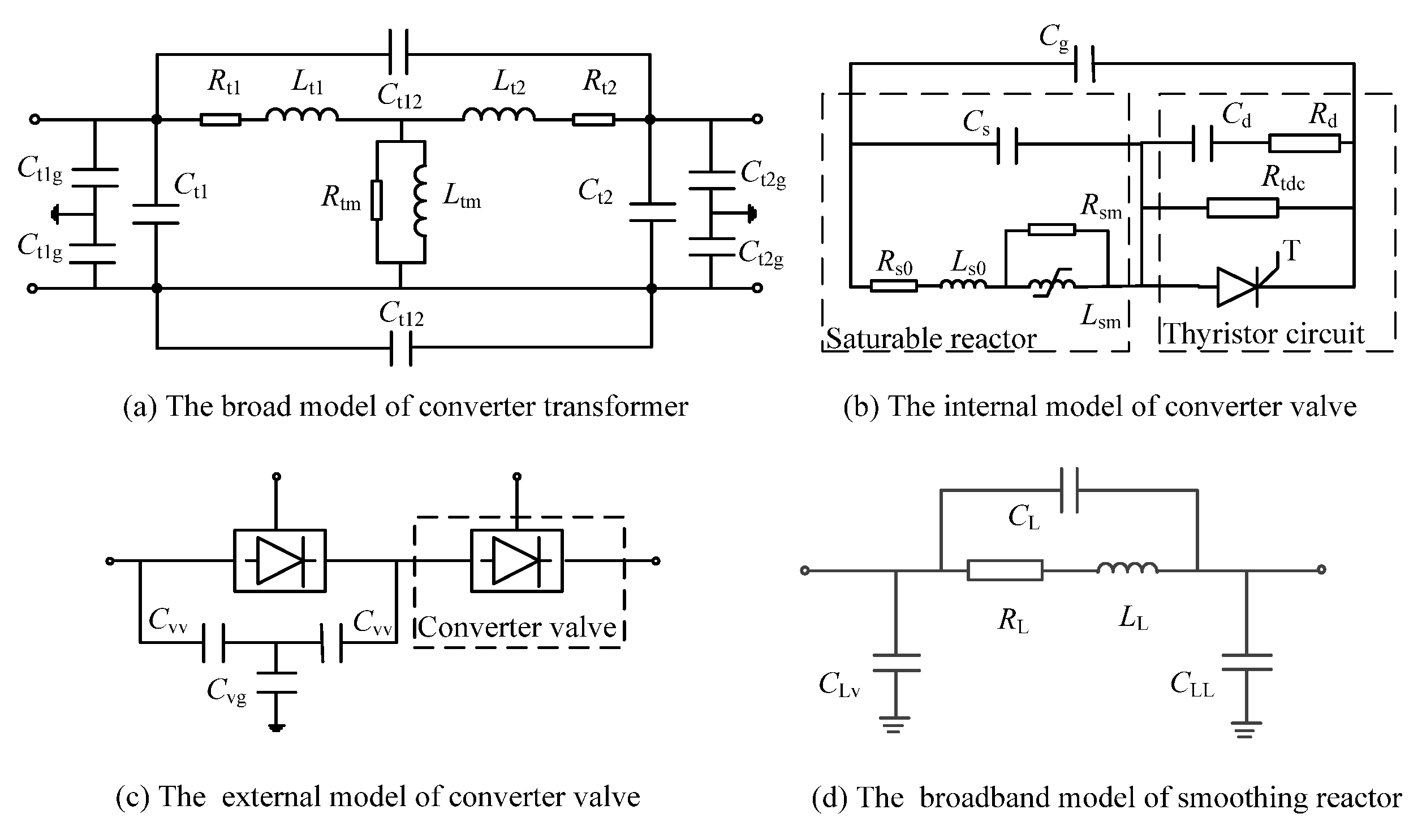
2.2.1. Converter Transformer

Limited by transportation ability, converter transformers used in UHVDC projects are assembled onsite by three single-phase converter transformers. Figure 3a shows the broadband model of single-phase converter transformer [28]. Rtm and Ltm denote the core loss resistance and the magnetization inductance; Rt1, Lt1, and Rt2, Lt2 represent the resistances and the inductances of the primary winding and the secondary winding, respectively. High frequency parameters include: Ct1 and Ct2 are parasitic capacitances inside the transformer windings; Ct1g and Ct2g are stray capacitances between the transformer windings and ground; Ct12 is the stray capacitance between the primary winding and the secondary winding. Besides, the stray inductances Lts of transformer windings are included in Lt1 and Lt2. Model parameters could be obtained from filed tests [29].

2.2.2. Wall Bushing

AC and DC switchyards are connected to the valve hall through wall bushings for mechanical support and electrical insulation. The electrical coupling effect between the wall bushing and surroundings is usually represented by a stray capacitance to ground at the level of pF, as shown in Figure 2a. Cbt and Cbp are placed at the valve side windings and pole lines, according to practical arrangements. Cab, Cac and Cbc in Figure 2b are obtained from the Y-Δ transformation of Cbt and Cbp. The values of stray capacitances are related with applied voltage levels and can be acquired from the product data sheets.

2.2.3. Converter Valve

The hierarchy of the broadband model of converter valve [30] are clearly illustrated in Figure 3, including the internal model in Figure 3b and the external model in Figure 3c. The internal model consists of the saturable reactor, the thyristor with auxiliary circuits and the grading capacitance Cg. In the saturable reactor, the resistance and the air core inductance of the primary winding are denoted as Rs0 and Ls0; the core loss resistance and the magnetizing inductance are denoted as Rsm and Lsm; the stray capacitance inside the primary winding is denoted as Cs. DC grading resistance Rtdc, damping resistance Rd and damping capacitance Cd are connected to the thyristor T in parallel. Noted that the valve model shown in Figure 3b is an integration of multiple series-connected valve modules, with the assumption that all these modules have the same characteristics.
The external model adopts a simple but representative method to describe the capacitive couplings inside and outside the converter valve, as shown in Figure 3c. The stray capacitance between the converter valve and surroundings is denoted as Cvg. The coupling effects between components inside the converter valve are represented by the stray capacitances Cvv. Parameters of stray capacitances can be obtained by filed measurements or electromagnetic field calculations [29].

2.2.4. Smoothing Reactor

Figure 3d depicts the broadband model of the smoothing reactor. The main circuit includes the inductance Ls and resistance Rs of the primary winding. The high frequency characteristics are represented by three stray capacitances: the parasitic capacitance across the primary winding CL, the stray capacitance to ground at valve side CLv and stray capacitance to ground at the line side CLL. These parameters could also be acquired from product data sheets.

2.3. Comparative Analysis

A comparative analysis between the conventional model and the broadband model has been conducted with reference to a practical ±1100 kV UHVDC transmission project in China [31]. PSCAD/EMTDC is chosen as the EMT program for circuit simulation. Model parameters, as presented in Appendix A Table A1, are all practical data, since there is no sense in determining them artificially. The effects of high frequency parameters, mainly stray capacitances, on the turn-off process can be observed from the differences between the transient valve voltage waveforms derived from these two models. To highlight the dependent influence of each high frequency parameter, the others are neglected when one parameter is considered.

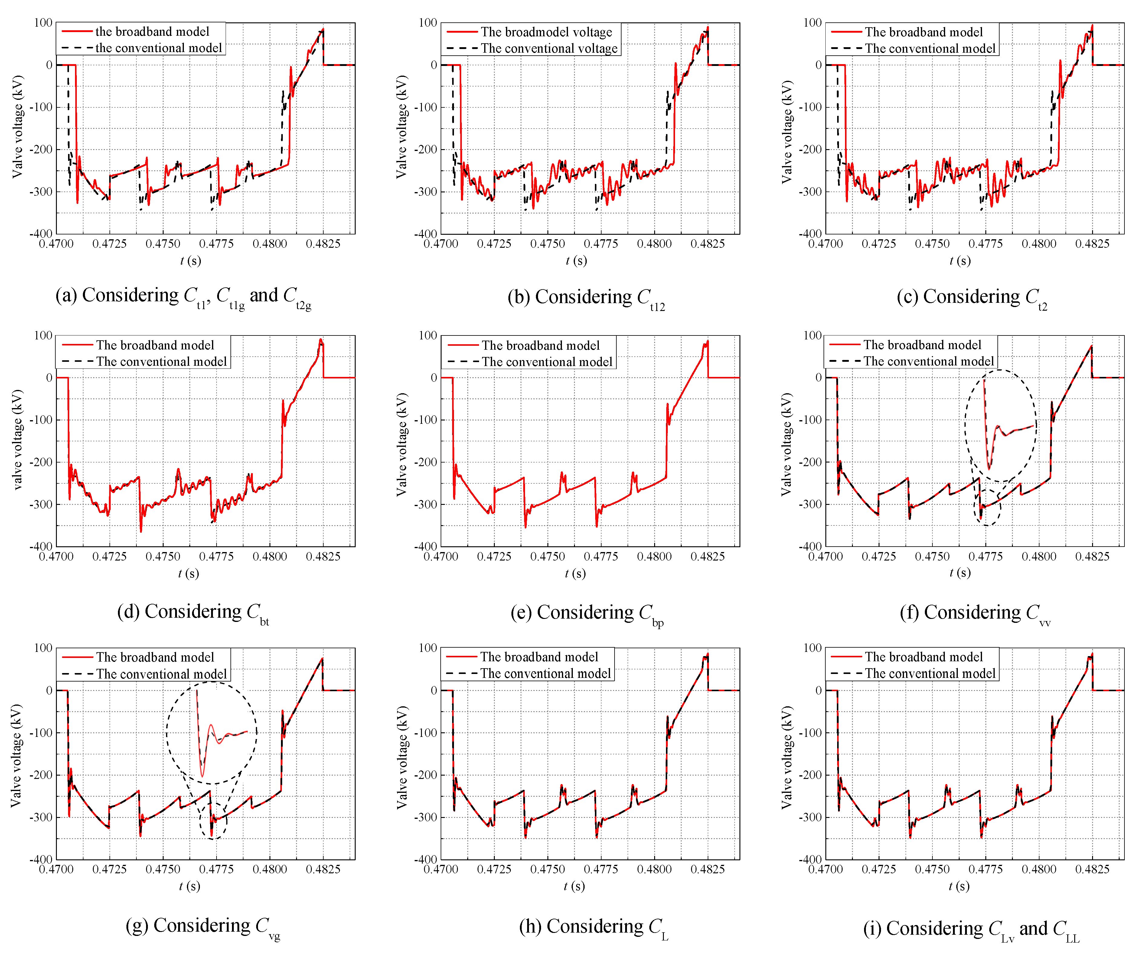
2.3.1. High Frequency Parameters in Converter Transformer

As shown in Figure 4a, the stray capacitances Ct1, Ct1g, and Ct2g have little effect on the transient voltage. The phase shift observed is introduced by the stray inductances Lts. A small phase shift may cause an obvious change of the valve voltage jump, which affects the amplitude of commutation overshoot. However, it can be compensated by modifying the values of Lt1 and Lt2, which is not the focus of our study.
As shown in Figure 4b,c, obvious voltage oscillations are imposed on the transient voltage derived from the conventional model when C12 and C22 are introduced. The valve voltage stresses are significantly affected by these voltage oscillations, which should be carefully considered in the damping circuit design.

2.3.2. High Frequency Parameters in Wall Bushings

As plotted in Figure 4d,e, the effect of Cbp on the transient voltage is negligible, while obvious high frequency voltage components arise with the introduction of Cbt. Considering that these two stray capacitances are placed at the AC side and DC side of the 6-pulse bridge separately, it indicates that the electrical coupling effect cannot be effectively transferred to other 6-pulse bridges through DC links.

2.3.3. High Frequency Parameters in Converter valves

Figure 4f,g illustrate the effect of converter valve high frequency parameters on the turn-off process. It is noted from Figure 4f that Cvv has little influence on the valve transient voltage. Though no obvious waveform change is observed, the magnitudes of voltage peaks have changed after the introduction of Cvg, as shown in Figure 4g. Since the main function of damping circuit is to limit commutation overshoots, it is necessary to consider the effects of Cvg when design the damping circuit.

2.3.4. High Frequency Parameters in Smoothing reactor

As plotted in Figure 4h,i, the high frequency characteristics of the smoothing reactor has no effect on the transient valve voltage. Again, it proves that DC links are not the transmission paths for electrical couplings between 6-pulse bridges.

2.4. Summary

It could be concluded from the above results that high frequency characteristics of valve equipment should be considered for an accurate description of the turn-off process. In practical engineering, even a change of 0.01 pu in PCOV evaluation has nonnegligible economic and engineering significances. It is reasonable and necessary to apply the broadband model into the analysis of issues related to the turn-off process of converter valve. Thus, the broadband model is used in the following sections for the performance analysis and the damping circuit parameter design.

3. Performance Indicators of Damping Circuit

The main purpose of installing damping circuits is to limit commutation overshoots. In addition, some other electrical quantities, such as the valve voltage rise rate and the turn-off power loss, should also be considered for a synthetic design of the damping circuit. This section quantifies the turn-off performances of converter valve by three specific parameters, which make up the basis of the damping circuit design. These characteristic curves shown in this section are derived from the broadband model of the ±1100 kV UHVDC project with parameters referred to Appendix A. For simplification, the values of voltage and power used below are per-unit values without special notations. The base voltage is selected as the magnitude of converter transformer valve side voltage Ev. The base power is selected as the rated DC transmission power Pn.

3.1. Commutation overshoot Uovst

When the outgoing valve is turned off, voltages across no-conducting valves will experience a rapid change, usually accompanied with oscillations and overshoots. The amplitude of commutation overshoot is mainly determined by three factors: the operating condition, the thyristor reverse recovery characteristics and the damping circuits. The information about the thyristor reverse recovery characteristics are specified in the product data sheets. Given that the delay angle α in the rectifier (or the extinction angle γ in the inverter) and the transmission power Pd are set at 17.5° and 1.1 pu, the voltages of nonconducting valves (V1, V4, V5, and V6) during the turn-off process of V1 are presented in Figure 5a,b. Subscripts refer to valve numbers. V5 and V6 are connected in parallel and the transient voltage across them are denoted by uv56(t). It is noticed that commutation overshoots produced in the rectifier are higher than those in the inverter. This is because the amplitude of the voltage jump at turn-off in the rectifier is normally larger than that in the inverter. That is why the rectifier model should be selected for PCOV calculation.
PCOV refers to the maximum repetitive stresses at thyristor valves, while another similar definition, CCOV, refers to the crest value of continuous operating voltage excluding commutation overshoots [32]. The ratio of PCOV to CCOV is defined as kovst. In practical engineering, kovst is usually designated a conservative value empirically based on the project voltage level. For example, the recommended kovst in the 1100 kV project is 1.17 [17]. In this way, the safe operation of converter valve is guaranteed while the insulation level of related equipment is increased.
Figure 5c,d show the transient valve voltage waveforms corresponding to different damping circuit parameters. It is found that the amplitude of commutation overshoot decreases as Cd increases, while the variation of Cd has little effect on the voltage oscillation frequency. On the contrary, a larger Rd usually indicates an earlier peak time and a faster attenuation of the transient valve voltage. Besides, there is always an optimal resistance of the damping resistor corresponding to the minimum commutation overshoot at a given damping capacitance, as can be seen from Figure 5e.

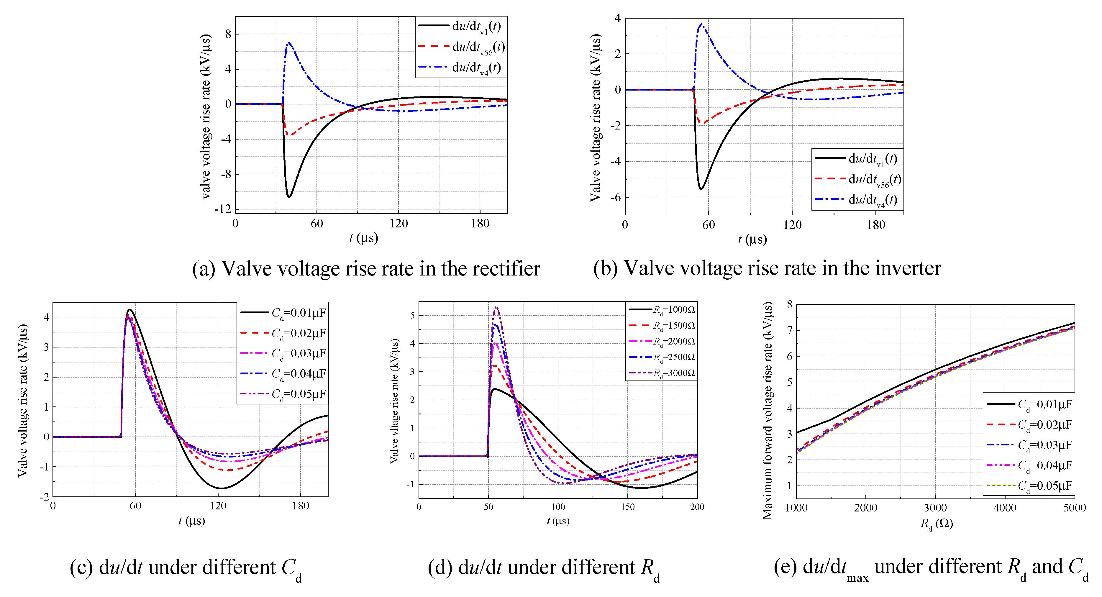
3.2. Forward Voltage Rise Rate du/dt

When the thyristor is just turned off, its ability to withstand a high forward voltage rise rate has not restored. Even if the thyristor is staying at the blocking state, it may also be damaged due to ungated turn-on resulted from capacitive displacement current, when a forward voltage with high rise rate is suddenly applied [5]. For safe operation, the maximum forward voltage rise rate du/dtmax should be limited under a specified critical value that is denoted as du/dtlim.
Figure 6a,b depict the valve voltage rise rates du/dt at V1 turn-off. Subscripts refer to valve numbers. As can be seen, the valve voltage rise rates reach to their peaks quickly and then decrease fast to be harmless. It should be noted that although the absolute value of the voltage change rate of the outgoing valve is larger than those in blocking valves, only the positive peak of du/dtv4 is really threatening. Moreover, the valve voltage rise rates in rectifier mode are obviously larger than that in the inverter mode, which indicates that an acceptable design for the rectifier is also suitable for the inverter.
Figure 6c,d give the curves of valve voltage rise rates calculated during the turn-off process. It is found that increasing Cd could only slightly reduce the maximum valve voltage rise rate, which is significantly affected by the variation of Rd. Specifically, a strong positive correlationship between du/dtmax and Rd is illustrated in Figure 6e.

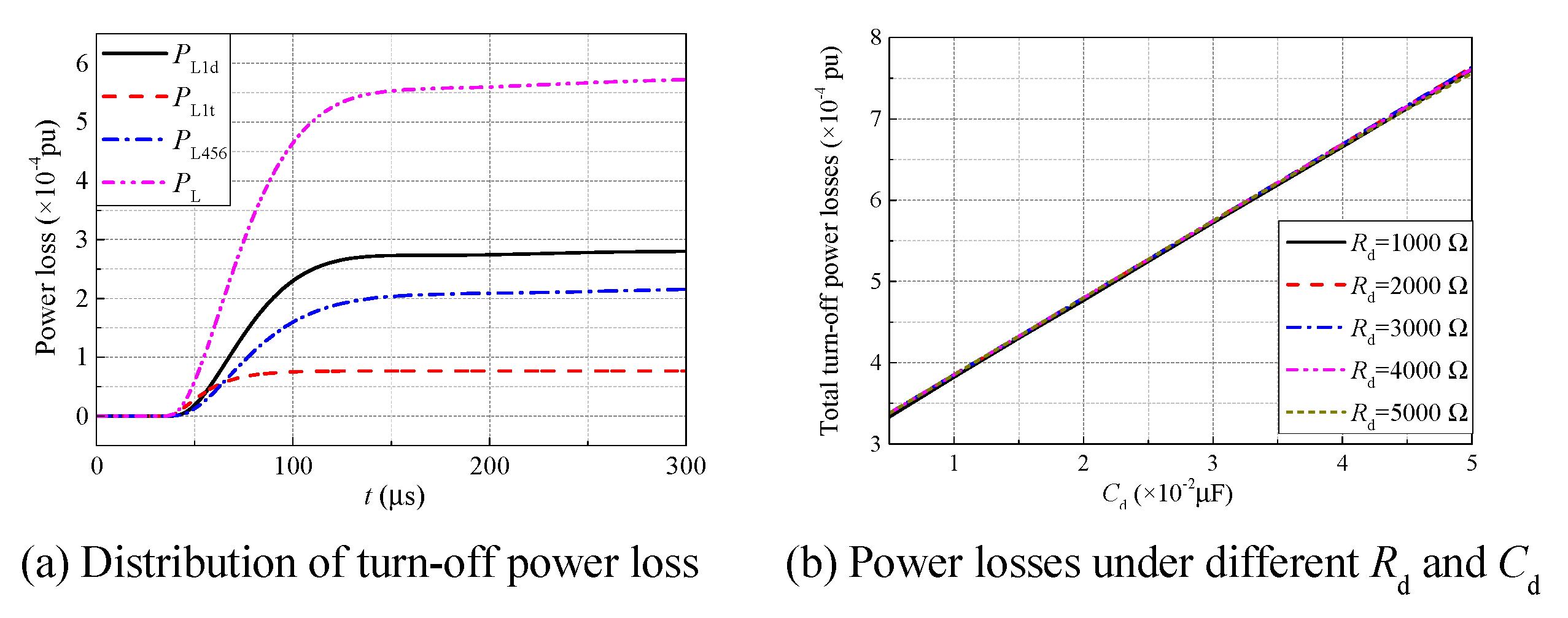
3.3. Turn-off Power Losses PL

During the valve turn-off process, the energy stored in the main circuit inductances feeds into the damping circuits to charge the damping capacitances, causing extra power losses on the damping resistance. Besides, the stored charges in the thyristors turned off are dissipated by reverse recovery currents [33], also resulting in power losses on both thyristors and damping resistances. According to practical engineering, 15% to 30% of the total power losses in the converter valve are the switching losses [34], which is necessary for the efficiency analysis. The capacity and investment costs of cooling equipment installed inside the converter valve are also affected by the switching loss [35]. Thus, it is necessary to minimize the turn-off power losses PL as much as possible.
The cumulative curves of turn-off power losses in different locations are shown in Figure 7a. PL1d and PL1t represent the power losses on damping resistances and thyristors inside the outgoing valve; PL456 represents the power losses at other blocking valves. As can be seen, most of the turn-off power losses are consumed by damping resistances. So, it is reasonable to take the turn-off power losses into account for the damping circuit design.
Figure 7b summarizes the total power losses during the turn-off process with respect to different damping circuit parameters. It can be easily found that there is a strong linear relationship between PL and Cd while the effect of damping resistance on power losses are negligible, although the most energy losses are consumed by damping resistors.

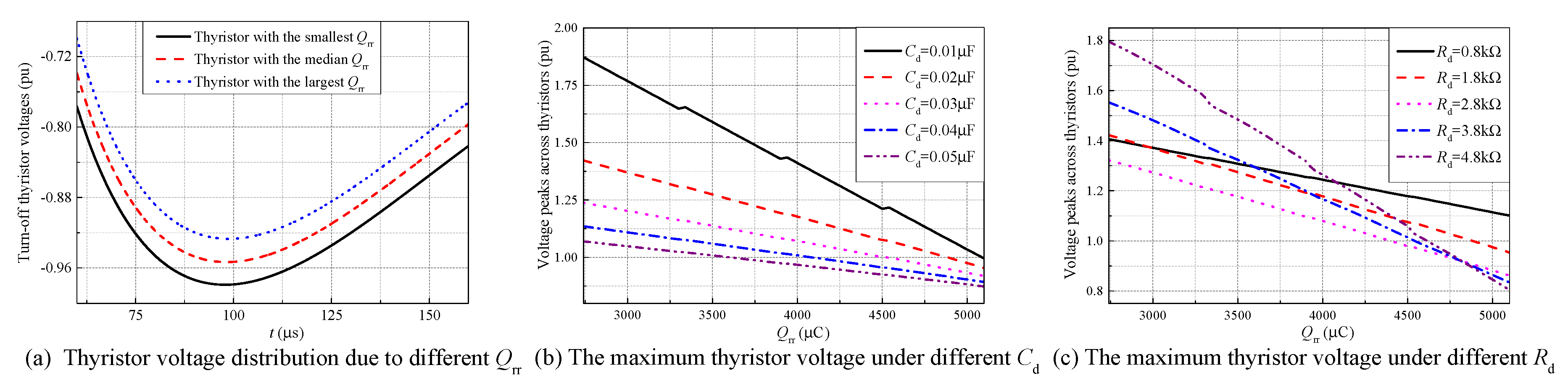
3.4. Unbalanced Voltage Distribution in Converter Valve

In general engineering applications, the whole converter valve is equivalent to a single thyristor circuit. In fact, hundreds of thyristors are series connected in one valve for safe operation under high voltage circumstances. Due to manufacturing tolerances, each thyristor may have different reverse recovery characteristics, such as reverse recovery charge Qrr and reverse recovery time trr, and thus experiences a different recovery process. trr is critical for inversion scheme since an improper trr may cause commutation failures. However, this potential threat is largely dependent on the operating condition of converter, not on the damping circuit. The dispersity of reverse recovery charge Qrr is thought to be a decisive factor for the uneven distribution of thyristor overvoltage during valve turn-off process [6]. According to the ±1100 kV HVDC project referred to in this article, a converter valve consists of 60 thyristors with an average reverse recovery charge at 3900 μC. Factory tests on samples show that the distribution range of Qrr will not exceed ±5%. Obviously, thyristor voltages considering the reverse recovery charge differences cannot be expressed in analytical form.
According to the general law, the distribution of Qrr in series-connected thyristors usually follow the probability characteristic of the random Gauss distribution. For convenient illustration, the equidistant distribution model is artificially set to demonstrate the dispersion of thyristor voltage. Figure 8a depicts the thyristor voltage distribution by three transient voltage waveforms corresponding to thyristors with different reverse recovery charges. As can be seen, the thyristor with a smaller Qrr will withstand a larger reverse voltage peak. It should also be noted that the forward voltage rise rates of thyristors are slightly different from the valve voltage rise rate due to unbalanced voltage distribution.
Figure 8b,c give the thyristor voltage stress under different damping circuit parameters, where the distribution range of Qrr is set as ±10% for better illustration. An inverse proportional relation between the damping capacitance Cd and the maximum thyristor voltage stresses can be easily observed. The relationship between the damping resistance Rd and the maximum thyristor voltage stress is similar to the quadratic relation of commutation overshoot to Rd. Calculation results shows that the differences between thyristor reverse recovery charges have a smaller effect on voltage stresses at valve level and the turn-off power losses.
Thus, the damping circuit parameter design should also consider the commutation overshoot and the forward voltage rise rate at the thyristor level when the unbalanced voltage distribution in the converter valve is taken into account, which cannot be completed by the analytical method.

3.5. Summary

According to the above analysis, there exist inevitable conflicts in the parameter design for the damping circuit, if different performance indicators were expected to be optimized separately. For example, the most efficient way to reduce the commutation overshoot is to increase Cd, which conversely results in more power losses. At a given Cd, if the value of Rd was determined by the optimal resistance, it is not guaranteed that du/dtmax are certainly limited under du/dtlim. Besides, the unbalanced voltage distribution in the converter valve should also be studied for damping circuit parameter design when the dispersion of reverse recovery characteristics is considered. Thus, a synthetical design method should been applied for the damping circuit.

4. Damping Circuit Parameters Design

4.1. Design Characteristics

The essential of damping circuit parameter design is to make a trade-off between decreasing commutation overshoot and reducing turn-off power losses, on the premise that the maximum valve voltage rise rate does not exceed the limitation. Mathematically this issue can be expressed as a multi-objective optimization problem. One approach for this kind of problem is to construct a comprehensive objective function that demonstrates the overall performance to be optimized. The weighted sum approach method can be used to integrate different performance indicators into the same objective function [36]. However, the physical senses of Uovst and PL are totally different. These two quantities with different dimensions should be further transformed for the establishment of an overall objective function. Thus, the concept of economic function is introduced below.
An economic evaluation for a specified UHVDC transmission project takes following four respects into account: construction and equipment investment, operation and maintenance, transmission losses, and interruption costs. The commutation overshoot has important influences on PCOV and the insulation level of the converter valve, which is directly related to the equipment investment. The turn-off power losses result in considerable transmission losses cost. In addition, it is one of the factors considered to determine the capacity of cooling equipment and thus affects the equipment investment indirectly. So, in the economy sense, an objective function composed of economic functions for performance indicators can be established:
f ( x ) = E o ( U ovst ( x ) ) + E L ( P L ( x ) ) + E c ( x )
where x is the variable vector to be optimized, i.e., (Rd, Cd); Eo and EL are economic functions of the commutation overshoot Uovst and the turn-off power losses PL. Another economic function Ec in (1) represent the part of equipment investment corresponding to damping circuits. Generally, the value of Ec has nothing to do with Rd, since the cost of damping resistors is negligible compared with that of damping capacitors.
Note that the unbalanced voltage distribution results in the necessity of device capacity margin and affects the selection of valve grading capacitance. To evaluate the impact of unbalanced voltage distribution, an economic function Eu is added to the objective function:
f ( x ) = E o ( U ovst ( x ) ) + E L ( P L ( x ) ) + E c ( x ) + E u ( U T max ( x ) U T min ( x ) U ovst ( x ) )
where UTmax(x) and UTmin(x) refer to the maximum and the minimum thyristor voltages respectively. The term (UTmax(x)−UTmin(x))/Uovst(x) represents the degree of voltage imbalance.
Now, the parameter design of damping circuit can be described as a constrained multi-variable optimization problem with the following mathematical form:
(P) minimize f(x)
subject to d u / d t max < d u / d t lim
R d > 0 , C d > 0
Additionally, du/dtmax here may refer to the maximum forward voltage rise rate either at the valve level or at the thyristor level under different considerations.

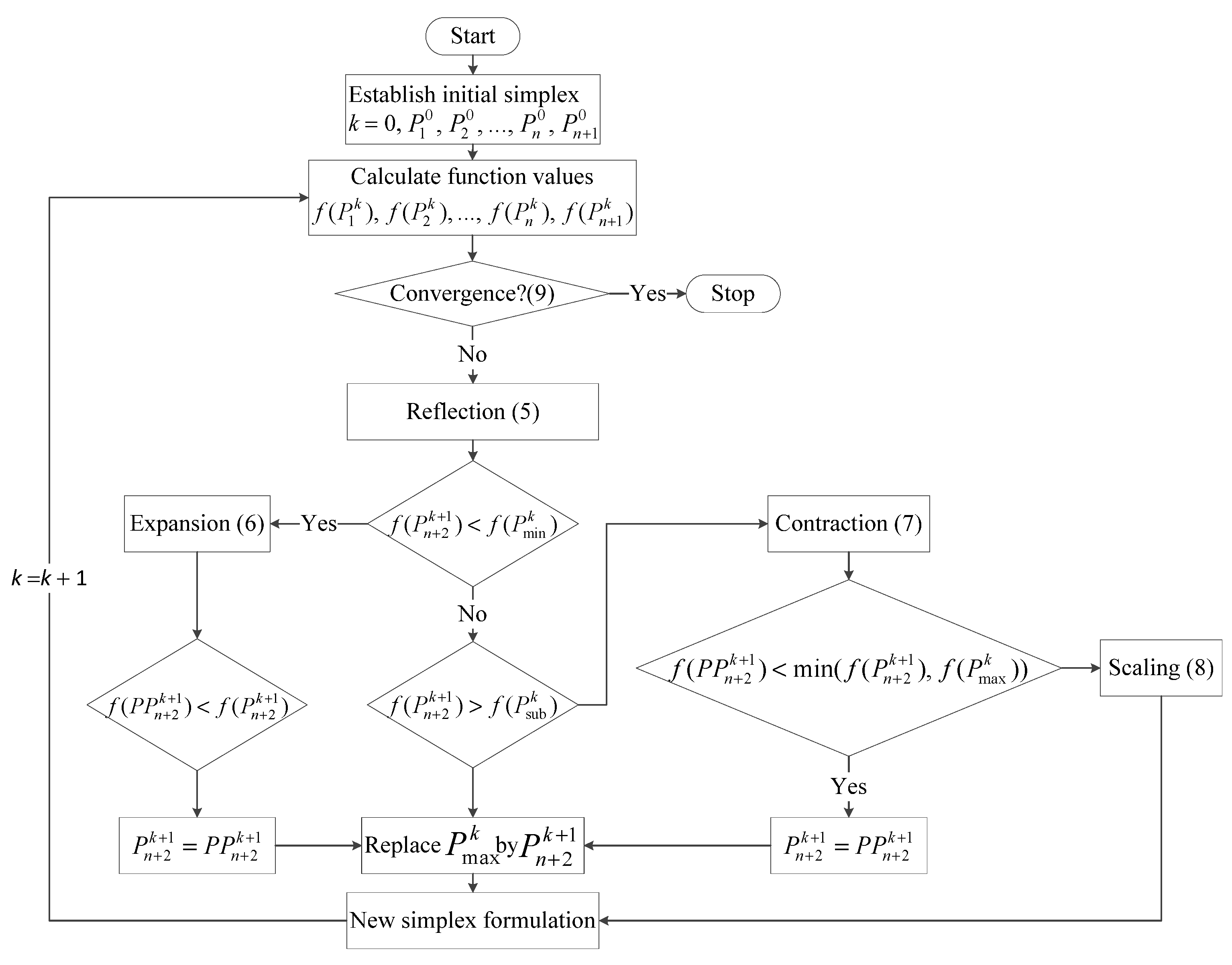
4.2. Optimization Algorithm
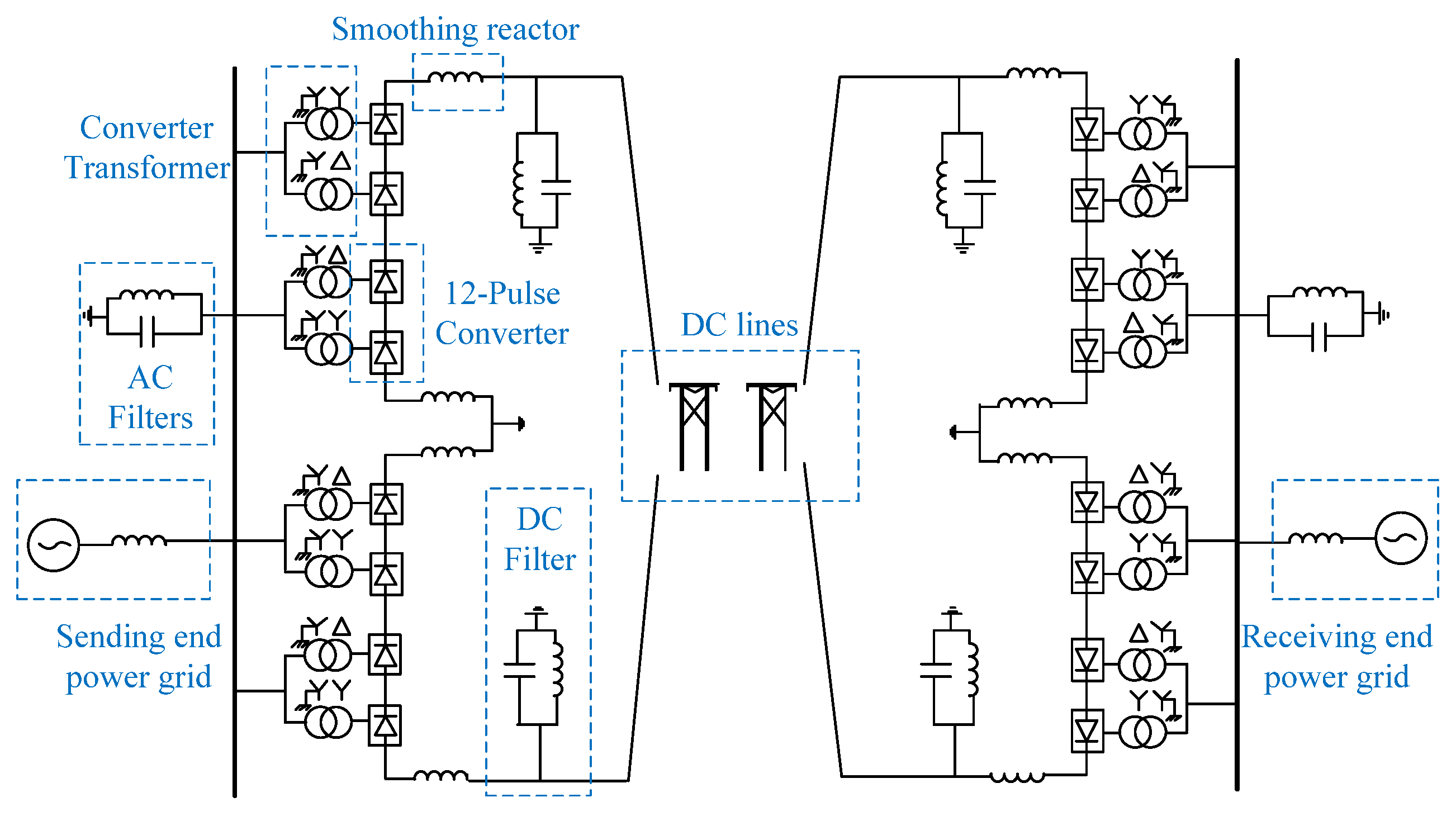
According to the availability of the derivatives of the objective function, optimization algorithms can be divided into two groups: the indirect search method and the direct search method. In the indirect search method, the Jacobian matrix of the objective function is solved firstly to obtain the extremum that is a candidate for the optimal result. Then this extremum should be substituted into the Hessian matrix for further verification. Although the optimization process convergence quickly, this method is still non-robust and time-consuming as the establishment and solution of the Jacobian matrix and the Hessian matrix is generally very difficult. Importantly, the derivatives of the objective function must be available in the indirect search method. However, it is not the case when the broadband model is applied.
The complex calculation circuit of the broadband model can be solved accurately through numerical calculation methods. Only the value of the objective function can be obtained in this way, where the indirect search method does not work. The direct search method, also called as the derivative-free algorithm, needs no more information about the objective function and continuously searches for the optimal point based on historical results and specific search rules. Despite the existence of iterations, it can be carried out in computer programs with high automation and convergency. Intelligent algorithms, including the genetic algorithm (GA), the particle swarm optimization (PSO), and so on, are representatives which are widely used currently for large scale nonlinear optimization problems. However, it is inappropriate to use these complex algorithms to deal with relatively simple problems such as the parameter design of damping circuit.
After analysis, a simple but efficient optimization algorithm—the nonlinear simplex method—was adopted in this paper. This method originates from the concept ‘evolutionary operation’ proposed by Box et al. [37], established by Spendley et al. [38] and developed for computer programming by Nelder and Mead [39]. Although researchers have modified some algorithm details for specific applications later [40,41], the core idea has remained unchanged.
Assuming that there are n variables, denoted as the variable vector x, to be optimized. f(x) represents the objective function to be minimized. In the n-dimensional variable space, an initial simplex composed of n+1 points should be determined firstly. The point set of the simplex at the kth iteration step are denoted as P i k ( 1 i n + 1 ) . Procedures for optimization are presented as follows:
Step 1. Reflection. According to the simplex at the previous iteration step k, a new point P n + 2 k + 1 can be calculated as:
P n + 2 k + 1 = ( 1 + α ) P k ¯ α P max k
where P max k is the point with the maximum objective function in the kth iteration step; P k ¯ is the centroid of the kth simplex excluding P max k ; α is a positive constant referred to as the reflection coefficient. P n + 2 k + 1 will take place of P max k for the next iteration step with remaining points.
Step 2. Expansion. After reflection, if f   ( P n + 2 k + 1 ) < f   ( P min k ) , where P min k corresponds to the point with the minimum objective function in the kth step, it indicates that a preferable point may exist at a longer distance in this search direction. So, a potential point P P n + 2 k + 1 is calculated as below:
P P n + 2 k + 1 = γ P n + 2 k + 1 + ( 1 γ ) P k ¯
where γ is a constant greater than 1.0 defined as the expansion coefficient. If f   ( P P n + 2 k + 1 ) < f   ( P n + 2 k + 1 ) , P P n + 2 k + 1 will replace P n + 2 k + 1 to go into the next iteration step. Otherwise, P P n + 2 k + 1 will be abandoned.
Step 3. Contraction. After reflection, if f   ( P n + 2 k + 1 ) > f   ( P sub k ) , where P sub k corresponds to the point with the submaximal objective function in the kth simplex, it indicates that a preferable point may exist at a shorter distance in this search direction. The potential point P P n + 2 k + 1 is calculated as below:
P P n + 2 k + 1 = β P v k + ( 1 β ) P k ¯
where β is a constant between 0.0 and 1.0 defined as the contraction coefficient; P v k is either P n + 2 k + 1 or P max k , whichever has the lower function value. If f   ( P P n + 2 k + 1 ) > min ( f   ( P n + 2 k + 1 ) ,   f   ( P max k ) ) , then P P n + 2 k + 1 will replace P n + 2 k + 1 for following iterations.
Step 4. Scaling. After contraction, if f   ( P P n + 2 k + 1 ) > min ( f   ( P n + 2 k + 1 ) ,   f   ( P max k ) ) , it indicates that the current simplex is too large to get closer to the optimal point. Thus, the simplex shrinks to half of the original:
P i k + 1 = ( P i k + P j k ) / 2 ,   ( i j , 1 i , j n + 1 )
where P i k + 1 is the new point produced by any two adjacent points P i k and P j k . Then the optimization process continues with the new point set P i k + 1 (1 ≤ i ≤ n).
Step 5. Convergence test. Repeating Step 1-4, the new formed simplex gradually moves to the neighborhood of the optimal point. The search process stops when the pre-set convergence condition (8) is satisfied. Standard deviation of function values in the simplex is used here.
i = 1 n + 1 ( f ( P i k ) f k ¯ ) n < ε
The flow chart of the optimization method is outlined in Figure 9. For inequality constraints, the augmented objective function F(x) is formed as:
F ( x ) = f ( x ) + p ( x )
where p(x) is the term of penalty function determined by the expressions of constraint conditions. The p(x) is set here to prevent invalid searches beyond the feasible region. Then, the augmented form of the objective function will be substituted into (5) ~ (9) to construct a constrained optimization.

5. Case Study

5.1. Problem Formulation

The design case presented here also refers to the ±1100 kV UHVDC project mentioned in previous sections. An augmented objective function F(x) of this design problem is proposed:
F ( x ) = f ( x ) + p 1 ( d v / d t max ) + p 2 ( x )
where p1 and p2 are penalty functions associated with (3) and (4), established as (12) and (13):
p 1 ( d v / d t ) = { 0 , d v / d t max < d v / d t lim a ( d v / d t max d v / d t lim ) , d v / d t max > d v / d t lim
p 2 ( x ) = { 0 , R d 0 , C d 0 b R d , R d < 0 , C d 0 b C d , R d 0 , C d < 0 b ( R d + C d ) , R d < 0 , C d < 0
where a and b are constant punish coefficients that are designated as 1000.0 in this case. In order to limit the bad effect of different numerical sizes of variables on the optimization algorithm, the units of Rd and Cd should be set as kΩ and μF, respectively. The values of Uovst, PL, and dv/dtmax are calculated based on the broadband model by EMT program.
In practice, detailed researches should be done to determine adequate economic functions. Here, linear functions are used to demonstrate the principle of the proposed optimization method:
E o ( U ovst ( x ) ) = w 1 U ovst ( x ) , E L ( P L ( x ) ) = w 2 P L ( x ) , E c ( x ) = w 3 C d , E u ( x ) = w 4 ( U T max ( x ) U T min ( x ) U ovst ( x ) )
where w1, w2, w3, and w4 are proportionality coefficients. According to engineering experiences, the values of w1, w2, w3, and w4 are set as 0.3, 30, 5, and 40.
Three important parameters for the optimization algorithm are the reflection coefficient α, the expansion coefficient γ, and the contraction coefficient β. According to parameter sensitivity study carried out in [42], we choose 1.0, 2.0, and 0.5 as the values of α, γ, and β, respectively. Besides, the convergent limit ε is set as 0.05.
Before the search process start, an initial simplex should be established. As the variable space is a two-dimensional plane, where Rd is selected as the x-axis and Cd is selected as the y-axis, the simplex takes a form of triangle. Specifically, we chose an isosceles triangle to be the initial simplex.

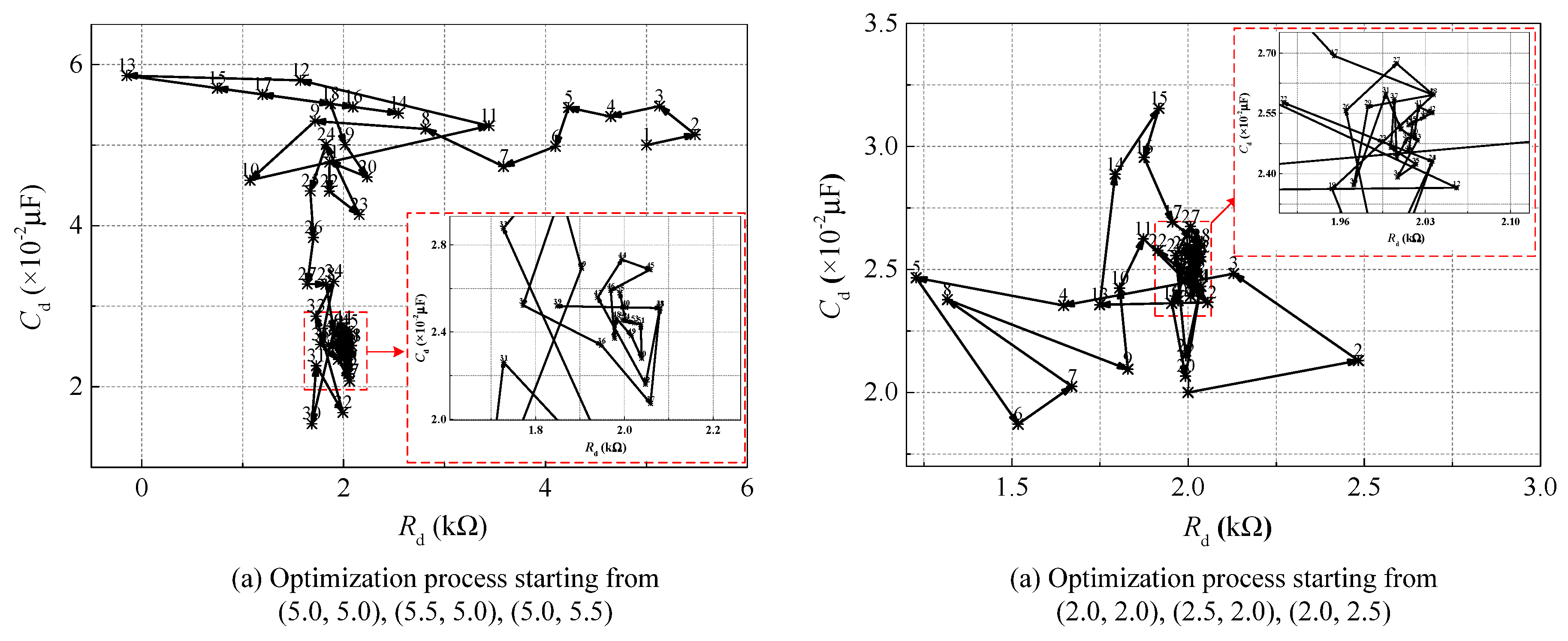
5.2. Optimization Results Considering Balanced Voltage Distribution

In this section, it is assumed that all thyristors have the same reverse recovery process and the objective function to be optimized is in the form of (1). Repeated optimization experiments are carried out for the same objective function and constraint conditions. The difference is these optimization processes start from different initial simplex, which are evenly distributed in a wide region, i.e., Rd∈[1000 Ω,5000 Ω] and Cd∈[0.01 μF,0.05 μF]. As can be seen from Table 1, all five optimization processes converge to the same small area, which demonstrates a good convergence of the proposed optimization method. The optimized parameters are Rd = 2000 Ω and Cd = 0.025 μF.
To further illustrate the principle of the proposed optimization method, Figure 10 depicts the development traces of parameter points starting from different initial simplex. Numbers tagged to points represent the order that they appear in the optimization process. When the current simplex stays away from the optimal point (see Figure 10a), the main evolution modes are reflection and expansion. The search process advances in an explicit direction and get close to the neighborhood of the optimal point quickly. When the current simplex is close to the optimal point (see Figure 10b), the main evolution modes are contraction and scaling. The area of new formed simplex decreases continuously and the new produced point gradually approaches to the optimal point, until the optimization process is stopped when the convergence condition is satisfied.
Table 2 makes a comparison between the practical damping circuit parameters (in the second row) and the optimized ones (in the third row). Giving a high priority to safe operation, the practical parameter setting tends to get lower commutation overshoots and valve voltage rise rate. However, greater power losses with higher economic cost arise from the selection of a larger damping capacitance. Contrarily, the optimized result pays more attention to the overall economic benefits, with the commutation overshoots and valve voltage rise rate increased but limited under the acceptable level.

5.3. Parameter Optimization Considering Unbalanced Voltage Distribution

In this section, the unbalanced voltage distribution arising from device dispersion is considered in damping circuit parameter design and the selected objective function is in the form of (2). Comparative studies have been carried out under assumptions for different distribution ranges of Qrr, i.e., ±5% and ±10%. The optimization results are shown in Table 3 and Table 4.
The optimization information given in above tables have shown a good convergence when Eu is added to the objective function. As can be seen, a larger damping capacitance is preferred to limit the degree of voltage imbalance due to wider distribution range of Qrr. The variation of damping resistance is relatively small, since it is not critical for the unbalanced voltage distribution. This effect has been illustrated in Figure 8. Table 5 summarizes the optimization results derived from different considerations for the dispersity of Qrr. Though the optimized parameters vary, it is found that little difference can be observed between cases in which the balanced voltage distribution is considered or the Qrr distribution range stays within ±5%.

5.4. Analysis of Economic Functions

Above, economic functions of the linear form are adopted for optimization. The function parameters are determined according to engineering practice. Since the forms and parameters of economic functions may be changed under specific considerations, it is necessary to study the adaptability of the proposed optimization method to various economic functions. For brief explanation, optimizations based on balanced voltage distribution is adopted in this section.
In the optimization process, different priorities are given to different performance indicators by adjusting the relative values of weighting coefficients. Table 6, Table 7, Table 8 has compared the optimized results under different w1, w2, and w3. For the sake of analysis, the others remain unchanged when one of them varies. As can be seen from Table 2 and Table 6, a larger w1 indicates that the main purpose of the optimization is to reduce commutation overshoots. Thus, the optimized results tend to increase the damping capacitance to get lower commutation overshoots, which inevitably cause higher turn-off power losses. On the contrary, if the optimization pays more attention to the power losses and the investment of damping circuits, w2 and w3 should be increased, so that small damping capacitances would occur in the optimized results which corresponds to higher commutation overshoots, as shown in Table 7 and Table 8. Noted that the variation of Rd in the optimized results is much smaller than that of Cd, since the value of damping resistance is strictly limited by the requirement of du/dtlim.
In linear form, the objective function to be minimized is represented as the weighted sum of turn-off performances indicators. Sometimes there is the necessity to change the forms of economic functions. For example, it is reasonable to set Eo and EL as quadratic functions considering that the difficulty of equipment manufacturing increases nonlinearly with the increase of voltage and power capacities. Since a large damping capacitance can be obtained by serval parallelly connected small capacitances, the nonlinearity of Ec is implicit and it is still expressed by a linear function. Thus, the new objective function can be expressed as:
f ( x ) = w 1 ( U ovst ( x ) ) 2 + w 2 ( P loss ( x ) ) 2 + w 3 C d
Table 9 summaries the optimization results with different initial simplex. All five optimization processes converge to the same small region inside which the optimized point is (1.8, 3.0). It can be seen that the proposed optimization method can be effectively applied to situations where the economy functions are nonlinear.

6. Conclusions

In this paper, the turn-off performances of converter valve have been analyzed by the broadband model firstly. Moreover, a reliable and flexible method for damping circuit parameters design are proposed. The main conclusions are presented below:
  • During the turn-off process of converter valve, the analytical calculation for the transient valve voltage has a low accuracy due to the application of low-frequency equipment models. High frequency parameters of valve equipment have non-negligible effects on the turn-off process, which are important for the damping circuit design. Thus, it is suggested to adopt the broadband model to evaluate the turn-off performances of converter valve based on numerical calculation methods.
  • There are inevitable conflicts existing in the parameters design of the damping circuit so that the turn-off performances cannot be optimized simultaneously. Besides, the unbalanced voltage distribution in the converter valve should also be studied for damping circuit parameter design. The damping circuit parameter design is essentially a constrained multi-objective optimization problem.
  • Parameters of the damping circuit can be optimized by the proposed optimization method consisting of EMT numerical calculation and the nonlinear simplex method. The concept of economic function is proposed to form a comprehensive objective function. The case study shows that the proposed optimization method has a good convergency.
  • The forms and parameters of economic functions can be adjusted according to the requirement of practical engineering. The optimization results presented in Section 5 have verified the reliability and flexibility of the proposed optimization method.

Author Contributions

Conceptualization, Z.X.; Methodology, Y.T. and Z.Z.; Validation, Y.T. and Z.Z.; Formal Analysis, Y.T.; Investigation, Y.T., Z.Z., and Z.X.; Writing-Review and Editing, Y.T., Z.Z., and Z.X.; Supervision, Z.X. and Z.Z. All authors have read and agreed to the published version of the manuscript.

Funding

This research received no external funding.

Conflicts of Interest

The authors declare no conflict of interest.

Abbreviations

The following abbreviations are used in this manuscript:
ACAlternating current
DCDirect current
HVDCHigh voltage direct current
UHVDCUltra high voltage direct current
LCCLine commutated converter
PCOVPeak value of continuous operating voltage
EMTElectromagnetic transient
PCCPoint of common coupling
ZcCommon impedance at point of common coupling
V1 ~ V6Converter valve, subscripts represent valve numbers
Rd and CdParameters of damping circuit: damping resistance and damping capacitance
ir(t)Reverse recovery current
UovstCommutation overshoot
du/dtForward valve voltage rise rate
PLPower losses during valve turn-off process
QrrReverse recovery charge
trrReverse recovery time
ELEconomic functions for power losses
EoEconomic functions for commutation overshoot
EcEconomic functions for damping circuit investments
EuEconomic functions for unbalanced voltage distribution
w1 ~ w4Constant coefficient of economic functions
a and bConstant punish coefficients
α, γ and βAlgorithm parameters: reflection, expansion and contraction coefficients

Appendix A

Main parameters of the referenced ±1100 kV HVDC project are as follows:
Table A1. Model Parameters of The Referenced ±1100 kV HVDC Project.
System/EquipmentParametersValues
AC switchyardRated voltage ( E v / 2 )750 kV
Short circuit capacity63 kA
Reactive compensation capacity6700 MVA
Converter transformerTransformer ratio750 kV / 235 kV
3-phase transformer capacity1800 MVA
Leakage reactance (Lt1 + Lt2)0.02 H
Winding resistance (Rt1+ Rt2)27 Ω
Stray inductance Lts2 mH
Stray capacitances inside windings Ct1/ Ct210/3.8 nF
Stray capacitances to ground Ct1g/ Ct2g16.99/3.31 nF
Stray capacitances between windings C121.91 nF
Wall bushingStray capacitance at valve side windings Cbt1.0 nF
Stray capacitance at pole lines Cbp0.4 nF
Converter valveRated voltage1100 kV
Rated transmission power12000MW
Smoothing inductance75 mH
Saturable reactorWinding resistance Rs00.1 mΩ
Air core inductance Ls06.3 μF
Core loss resistance Rsm0.32 mΩ
Magnetizing inductance Lsm 2.8 mH
Stray capacitance Cs5.0 nF
ThyristorcircuitsDC grading resistance Rtdc5.76 MΩ
Damping resistance Rd1800 Ω
Damping capacitance Cd0.03 μF
Reverse recovery charge Qrr3900 μC
Distribution range of Qrr±5%
Grading capacitance Cg1.0 uF
Stray capacitances between components Cvv120 pF
Stray capacitances to ground Cvg200 pF
Smoothing reactorMain inductance LL75 mH
winding resistance10 mΩ
Stray capacitance at valve side CLv412.5 pF
Stray capacitance at valve side CLL412.5 pF
Stray capacitance across winding CL534 pF
DC systemRated voltage Udc1100 kV
Rated power transmission Pn12000 MW

References

  1. Jiang, L.; Zhang, L.; Zou, L.; Zhao, T. Investigation on an optimized topology design of the HVDC converter valve to mitigate commutation failure. In Proceedings of the 2016 IEEE 11th Conference on Industrial Electronics and Applications (ICIEA), Hefei, China, 5–7 June 2016; pp. 343–347. [Google Scholar]
  2. Zha, K.; Cao, J.Z.; Ouyang, W.; Sun, B.; Gao, C.; Luan, H. Design of 6250A/±800kV UHVDC converter valve. In Proceedings of the 13th IET International Conference on AC and DC Power Transmission (ACDC 2017), Manchester, UK, 14–16 February 2017; pp. 1–6. [Google Scholar]
  3. Kumar, A.; Jhampati, S.; Suri, R. HVDC Converter Stations Design for LCC Based HVDC Transmission System-Key Consideration. In Proceedings of the 14th IEEE India Council International Conference, Roorkee, India, 15–17 December 2017; pp. 1–6. [Google Scholar]
  4. Gou, R. Research on 1100-kV/5500-A Ultra-High Voltage Thyristor Valve Key Technology and Its Application. IEEE Trans. Power Electron. 2019, 34, 10524–10533. [Google Scholar] [CrossRef]
  5. Woodhouse, M.L. Voltage and Current Stresses on HVDC Valves. IEEE Trans. Power Deliv. 1987, 2, 199–206. [Google Scholar] [CrossRef]
  6. Yue, K.; Pang, L.; You, H.; Li, S.; Kong, D.; Li, Y.; Zhang, Q.; Liu, L. Reverse recovery characteristics of high power thyristors in HVDC converter valve. IEEE Trans. Dielectr. Electr. Insul. 2017, 24, 2132–2140. [Google Scholar] [CrossRef]
  7. Arrillaga, J.; Ramsbottom, M.J. Commutation transients in h.v.d.c. convertors during normal and abnormal conditions. Proc. Inst. Electr. Eng. 1970, 117, 1324–1332. [Google Scholar] [CrossRef]
  8. Chang, W.L.; Song, B.P. Design of a thyristor snubber circuit by considering the reverse recovery process. IEEE Trans. Power Electron. 1988, 3, 440–446. [Google Scholar] [CrossRef]
  9. Tennakoon, S.B.; Woodhouse, M.L. Calculation of valve damping circuit losses in 12-pulse HVDC convertors. IEEE Trans. Power Deliv. 1992, 7, 1002–1008. [Google Scholar] [CrossRef]
  10. Ma, C.L.; Lauritzen, P.O.; Turkes, P.; Mattausch, H.J.; Liu, S.; Xu, Z. A physically-based lumped-charge SCR model. In Proceedings of the IEEE Power Electronics Specialist Conference-PESC ’93, Seattle, WA, USA, 20–24 June 1993; pp. 53–59. [Google Scholar]
  11. McMurray, W. Optimum Snubbers for Power Semiconductors. IEEE Trans. Ind. Appl. 1972, 5, 593–600. [Google Scholar] [CrossRef]
  12. Burdio, J.M.; Martinez, A. A unified discrete-time state-space model for switching converters. IEEE Trans. Power Electron. 1995, 10, 694–707. [Google Scholar] [CrossRef]
  13. Zhang, J.; Tang, G.; Wen, J.; Zha, K. Dynamic Modelling of the Turn off Performance of High Voltage Power Thyristor. Power Electron. 2015, 49, 50–53. (In Chinese) [Google Scholar]
  14. Revankar, G.N.; Srivastava, P.K. Turnoff Model of an SCR. IEEE Trans. Ind. Electron. Contr. Instrum. 1975, 4, 507–510. [Google Scholar] [CrossRef]
  15. Chokhawala, R.S.; Carroll, E.I. A snubber design tool for P-N junction reverse recovery using a more accurate simulation of the reverse recovery waveform. IEEE Trans. Ind. Appl. 1991, 27, 74–84. [Google Scholar] [CrossRef]
  16. Gao, C.; Zhang, J.; Zhou, J.; Yin, C. Study on the Calculation of the Commutation Overshoot of HVDC Valve Based on the Piecewise Fitting of Reverse Recovery Current of Thyristor. Proc. CSEE 2018, 38, 547–556. (In Chinese) [Google Scholar]
  17. Zhou, P.; He, H.; Dai, M.; Wan, L. Selection of Arresters Arrangement, Parameters and Apparatuses Insulation Levels for ±1100 kV DC Converter Station. High Volt. Eng. 2014, 40, 2871–2884. (In Chinese) [Google Scholar]
  18. Huang, H.; Fang, T.; Liu, L.; Zhang, X.; Chen, C.; Cao, D. Modeling of reverse recovery characteristic and optimal design of resistance and capacitance parameters for thyristor converter valve. Electr. Power Autom. Equip. 2017, 37, 187–190. [Google Scholar]
  19. ABB. Design of RC Snubbers for Phase Control Applications; Application note; ABB: Zurich, Switzerland, 2008; pp. 7–8. [Google Scholar]
  20. Beausejour, Y.; Karady, G. Valve Damping Circuit Design for HVDC Systems. IEEE Trans. Power Appar. Syst. 1973, 5, 1615–1621. [Google Scholar] [CrossRef]
  21. Undeland, T.M.; Petterteig, A.; Hauknes, G.; Adnanes, A.K.; Garberg, S. Diode and thyristor turn-off snubbers simulation by KREAN and an easy to use design algorithm. In Proceedings of the Conference Record of the 1988 IEEE Industry Applications Society Annual Meeting, Pittsburgh, PA, USA, 2–7 October 1988; pp. 647–654. [Google Scholar]
  22. Gole, A.M.; Filizadeh, S.; Menzies, R.W.; Wilson, P.L. Optimization-enabled electromagnetic transient simulation. IEEE Trans. Power Deliv. 2005, 20, 512–518. [Google Scholar] [CrossRef]
  23. Tong, W.; Li, H.; Fu, P.; Song, Z.; Wang, K.; Wang, S.; Zhang, X. Parameter Optimization of Thyristor Snubber Circuit in LSTF Quench Protection System. IEEE Access 2019, 7, 81257–81265. [Google Scholar] [CrossRef]
  24. Karady, J.; Gilsig, T. The Calculation of Turn-off Overvoltages in a High Voltage dc Thyristor Valve. IEEE Trans. Power Appar. Syst. 1972, 2, 565–574. [Google Scholar] [CrossRef]
  25. Qi, L.; Guan, L.; Shuai, Q.; Wen, J.; Cui, X.; Wei, X.; Fang, C. Building and Analysis of Integrated Wideband Models for Key Components in HVDC Converter Valve Systems. IEEE Trans. Electromagn. Compat. 2014, 56, 1697–1706. [Google Scholar] [CrossRef]
  26. Jiao, C.; Yao, A.; Liu, X. Broadband models for key equipment in high-voltage DC converter stations. IET Power Electron. 2016, 9, 1761–1767. [Google Scholar] [CrossRef]
  27. Qi, L.; Shuai, Q.; Cui, X.; Fang, C.; Sun, H.; Wei, X.; Gao, C. Parameter Extraction and Wideband Modeling of ±1100 kV Converter Valve. IEEE Trans. Power Deliv. 2017, 32, 1303–1313. [Google Scholar] [CrossRef]
  28. Valii, M.; Bigdeli, M.; Hojjatiparast, F. Transient model parameters identification of transformer based on PSO algorithm. In Proceedings of the 2013 3rd International Conference on Electric Power and Energy Conversion Systems, Istanbul, Turkey, 2–4 October 2013; pp. 1–5. [Google Scholar]
  29. Zhang, X.; Yu, Z.; He, J.; Wang, Y.; Zeng, R. The broadband frequency characteristics of major equipment in the ±800 kV converter station and their influences to the short-circuit fault transient. Electr. Power Syst. Res. 2017, 147, 302–309. [Google Scholar] [CrossRef]
  30. Ying, C.; Xu, Z.; Luo, C. Analysis of high-frequency interference characteristics of UHVDC converters. J. Eng. 2019, 2019, 1937–1941. [Google Scholar] [CrossRef]
  31. Lou, Y.; Li, Z.; Xie, L.; Wan, L. Research on overvoltage and minimum air clearance on 1000 kV AC side of converter transformer in ±1100 kV Guquan converter station. J. Eng. 2019, 2019, 2159–2164. [Google Scholar]
  32. IEC 60071-5: Insulation Co-Ordination-Part 5: Procedures for High-Voltage Current (HVDC) Converter Stations; IEC: Geneva, Switzerland, 2014; pp. 28–29.
  33. Li, W.; Kong, D.; Yue, K.; Li, S.; Sun, W.; Peng, J.; Wang, K.; Tan, X.; Liu, X.; Zhang, Q.; et al. Study on reverse recovery characteristics of thyristor used in HVDC converter valve. In Proceedings of the 12th IET International Conference on AC and DC Power Transmission (ACDC 2016), Beijing, China, 28–29 May 2016; pp. 1–5. [Google Scholar]
  34. Cepek, M.; Douville, J.; Fecteau, G.; Malewski, R. Loss measurement in high voltage thyristor valves. IEEE Trans. Power Deliv. 1994, 9, 1222–1236. [Google Scholar] [CrossRef]
  35. Lips, H.P. Water cooling of HVDC thyristor valves. IEEE Trans. Power Deliv. 1994, 9, 1830–1837. [Google Scholar] [CrossRef]
  36. Chowdhury, D.; De, B.P.; Maji, K.B.; Ghosh, S.; Kar, R.; Mandal, D. Optimization of Electrical Parameters for the Gate Stack Double Gate (GSDG) MOSFET using Simplex-PSO Algorithm. In Proceedings of the 2019 Devices for Integrated Circuit (DevIC), Kalyani, India, 23–24 March 2019; pp. 334–336. [Google Scholar]
  37. Box George, E.P. Evolutionary Operation: A Method for Increasing Industrial Productivity. J. R. Stat. Soc. Ser. C (Appl. Stat.) 1957, 6, 81–101. [Google Scholar]
  38. Spendley, W.; Hext, G.R.; Himsworth, F.R. Sequential Application of Simplex Designs in Optimisation and Evolutionary Operation. Technometrics 1962, 4, 441–461. [Google Scholar] [CrossRef]
  39. Neleder, J.A.; Mead, R. A simplex method for function minimization. Comput. J. 1965, 7, 308–313. [Google Scholar] [CrossRef]
  40. Huang, Y.; McColl, W.F. An improved simplex method for function minimization. In Proceedings of the 1996 IEEE International Conference on Systems, Man and Cybernetics. Information Intelligence and Systems (Cat. No. 96CH35929), Beijing, China, 14–17 October 1996; pp. 1702–1705. [Google Scholar]
  41. Takahama, T.; Sakai, S. Constrained optimization by applying the α constrained method to the nonlinear simplex method with mutations. IEEE Trans. Evol. Comput. 2005, 9, 437–451. [Google Scholar] [CrossRef]
  42. Wang, P.C.; Shoup, T.E. Parameter sensitivity study of the Nelder–Mead Simplex Method. Adv. Eng. Softw. 2011, 42, 529–533. [Google Scholar] [CrossRef]
Figure 1. Basic Topology of UHVDC Transmission Project.
Energies 13 01059 g001
Figure 2. Conventional Model for Turn-off Process.
Energies 13 01059 g002
Figure 3. The Broadband Models of Valve Equipment.
Energies 13 01059 g003
Figure 4. Comparisons of Transient Valve Voltages Obtained from Two Different Models.
Energies 13 01059 g004
Figure 5. Characteristics of Commutation Overshoot.
Energies 13 01059 g005
Figure 6. Characteristics of Forward Valve Voltage Rise Rate.
Energies 13 01059 g006
Figure 7. Characteristics of Turn-off Power Losses.
Energies 13 01059 g007
Figure 8. Characteristics of Unbalanced Voltage Distribution of Converter Valve.
Energies 13 01059 g008
Figure 9. Algorithm Flow Chart.
Energies 13 01059 g009
Figure 10. Optimization Processes from Different Initial Simplex.
Energies 13 01059 g010
Table 1. Summary of Optimization Results Considering Balanced Voltage Distribution.
Initial SimplexTermination PointIterationsf(x)
(1.0, 1.0), (1.0, 1.5), (1.5, 1.0)(2.02, 2.55)4992.99
(2.0, 2.0), (2.0, 2.5), (2.5, 2.0)(2.02, 2.53)4692.99
(3.0, 3.0), (3.0, 3.5), (3.5, 3.0)(2.02, 2.54)4892.99
(4.0, 4.0), (4.0, 4.5), (4.5, 4.0)(2.01, 2.52)4393.00
(5.0, 5.0), (5.0, 5.5), (5.5, 5.0)(2.00, 2.45)5593.02
Table 2. Comparison Between The Practical and The Optimized Parameters.
ItemRd (kΩ)Cd (×10−2μF)du/dtmax(kV/μs)kovstf(x)
Practical1.83.03.651.1493.95
Theoretical2.02.53.971.1593.03
Table 3. Optimization Results Considering Unbalanced Voltage Distribution (±5% Qrr Distribution).
Initial SimplexTermination PointIterationsf(x)
(1.0, 1.0), (1.0, 1.5), (1.5, 1.0)(1.98, 2.59)5398.57
(2.0, 2.0), (2.0, 2.5), (2.5, 2.0)(1.96, 2.68)5698.53
(3.0, 3.0), (3.0, 3.5), (3.5, 3.0)(1.95, 2.66)4998.53
(4.0, 4.0), (4.0, 4.5), (4.5, 4.0)(1.96, 2.70)5298.56
(5.0, 5.0), (5.0, 5.5), (5.5, 5.0)(1.97, 2.65)5598.55
Table 4. Optimization Results Considering Unbalanced Voltage Distribution (±10% Qrr Distribution).
Initial SimplexTermination PointIterationsf(x)
(1.0, 1.0), (1.0, 1.5), (1.5, 1.0)(1.88, 2.95)59106.32
(2.0, 2.0), (2.0, 2.5), (2.5, 2.0)(1.88, 2.94)57106.37
(3.0, 3.0), (3.0, 3.5), (3.5, 3.0)(1.90, 2.93)58106.37
(4.0, 4.0), (4.0, 4.5), (4.5, 4.0)(1.84, 2.97)60106.36
(5.0, 5.0), (5.0, 5.5), (5.5, 5.0)(1.85, 3.01)62106.31
Table 5. Comparisons of Optimized Parameters Considering Different Qrr Distribution Ranges.
DistributionRd (kΩ)Cd (×10−2μF)du/dtmax(kV/μs)kovstf(x)
02.02.53.971.1593.03
±5%1.952.663.971.1598.53
±10%1.853.013.991.14106.31
Table 6. Effects of w1 on Optimization Results.
w1Rd (kΩ)Cd (×10−2μF)PL(×10−4 pu)kovst
0.13.290.833.871.29
0.61.873.216.311.13
0.91.714.287.401.11
Table 7. Effects of w2 on Optimization Results.
w2Rd (kΩ)Cd (×10−2μF)PL(×10−4 pu)kovst
152.321.955.011.17
602.391.774.831.18
902.441.684.741.19
Table 8. Effects of w3 on Optimization Results.
w3Rd (kΩ)Cd (×10−2μF)PL(×10−4 pu)kovst
2.51.952.986.071.14
7.52.651.414.461.20
102.881.144.191.23
Table 9. Summary of Optimization Results Based on Quadratic Functions.
Initial SimplexTermination PointIterationsf(x)
(1.0, 1.0), (1.0, 1.5), (1.5, 1.0)(1.80, 2.98)66123.56
(2.0, 2.0), (2.0, 2.5), (2.5, 2.0)(1.80, 3.01)54123.53
(3.0, 3.0), (3.0, 3.5), (3.5, 3.0)(1.80, 3.01)60123.54
(4.0, 4.0), (4.0, 4.5), (4.5, 4.0)(1.81, 3.04)65123.53
(5.0, 5.0), (5.0, 5.5), (5.5, 5.0)(1.81, 3.02)60123.51

